EP2965105B1 - Messung des elektrischen stroms in einem leiter - Google Patents
Messung des elektrischen stroms in einem leiter Download PDFInfo
- Publication number
- EP2965105B1 EP2965105B1 EP13876874.2A EP13876874A EP2965105B1 EP 2965105 B1 EP2965105 B1 EP 2965105B1 EP 13876874 A EP13876874 A EP 13876874A EP 2965105 B1 EP2965105 B1 EP 2965105B1
- Authority
- EP
- European Patent Office
- Prior art keywords
- sensor
- current
- magnetic field
- conductor
- signal component
- Prior art date
- Legal status (The legal status is an assumption and is not a legal conclusion. Google has not performed a legal analysis and makes no representation as to the accuracy of the status listed.)
- Active
Links
- 239000004020 conductor Substances 0.000 title claims description 107
- 230000005291 magnetic effect Effects 0.000 claims description 207
- 239000000758 substrate Substances 0.000 claims description 111
- 229910000859 α-Fe Inorganic materials 0.000 claims description 100
- 238000001914 filtration Methods 0.000 claims description 80
- 230000008859 change Effects 0.000 claims description 53
- 229910052751 metal Inorganic materials 0.000 claims description 52
- 239000002184 metal Substances 0.000 claims description 52
- 230000004927 fusion Effects 0.000 claims description 39
- 230000004044 response Effects 0.000 claims description 29
- 230000005672 electromagnetic field Effects 0.000 claims description 9
- 239000012141 concentrate Substances 0.000 claims description 8
- 238000000034 method Methods 0.000 description 29
- 230000004907 flux Effects 0.000 description 23
- 239000003990 capacitor Substances 0.000 description 19
- 230000013011 mating Effects 0.000 description 16
- 239000004065 semiconductor Substances 0.000 description 14
- 230000035945 sensitivity Effects 0.000 description 12
- 230000005355 Hall effect Effects 0.000 description 11
- 238000010586 diagram Methods 0.000 description 11
- 230000000153 supplemental effect Effects 0.000 description 8
- 230000005684 electric field Effects 0.000 description 7
- 230000009977 dual effect Effects 0.000 description 6
- 238000005259 measurement Methods 0.000 description 6
- 230000005294 ferromagnetic effect Effects 0.000 description 5
- 230000001939 inductive effect Effects 0.000 description 5
- 239000000463 material Substances 0.000 description 5
- 239000011159 matrix material Substances 0.000 description 5
- 230000008878 coupling Effects 0.000 description 4
- 230000001808 coupling effect Effects 0.000 description 4
- 238000010168 coupling process Methods 0.000 description 4
- 238000005859 coupling reaction Methods 0.000 description 4
- 230000036039 immunity Effects 0.000 description 4
- 239000013528 metallic particle Substances 0.000 description 4
- 230000010363 phase shift Effects 0.000 description 4
- 239000000523 sample Substances 0.000 description 4
- 230000005669 field effect Effects 0.000 description 3
- 238000010438 heat treatment Methods 0.000 description 3
- 229910044991 metal oxide Inorganic materials 0.000 description 3
- 150000004706 metal oxides Chemical class 0.000 description 3
- 229920000642 polymer Polymers 0.000 description 3
- 229920005989 resin Polymers 0.000 description 3
- 239000011347 resin Substances 0.000 description 3
- 230000008646 thermal stress Effects 0.000 description 3
- 238000004804 winding Methods 0.000 description 3
- 229910000831 Steel Inorganic materials 0.000 description 2
- 229910045601 alloy Inorganic materials 0.000 description 2
- 239000000956 alloy Substances 0.000 description 2
- 230000004888 barrier function Effects 0.000 description 2
- 230000015572 biosynthetic process Effects 0.000 description 2
- 239000000872 buffer Substances 0.000 description 2
- 238000001514 detection method Methods 0.000 description 2
- 230000006870 function Effects 0.000 description 2
- 238000009413 insulation Methods 0.000 description 2
- 239000000696 magnetic material Substances 0.000 description 2
- 230000008569 process Effects 0.000 description 2
- 239000010959 steel Substances 0.000 description 2
- 208000031872 Body Remains Diseases 0.000 description 1
- 229910000531 Co alloy Inorganic materials 0.000 description 1
- 229910000640 Fe alloy Inorganic materials 0.000 description 1
- 229910000914 Mn alloy Inorganic materials 0.000 description 1
- 229910000990 Ni alloy Inorganic materials 0.000 description 1
- -1 NiFeMo Inorganic materials 0.000 description 1
- 239000011324 bead Substances 0.000 description 1
- 230000000903 blocking effect Effects 0.000 description 1
- 239000000919 ceramic Substances 0.000 description 1
- 230000006835 compression Effects 0.000 description 1
- 238000007906 compression Methods 0.000 description 1
- 230000001419 dependent effect Effects 0.000 description 1
- 238000003745 diagnosis Methods 0.000 description 1
- 230000003993 interaction Effects 0.000 description 1
- 238000002955 isolation Methods 0.000 description 1
- 238000004519 manufacturing process Methods 0.000 description 1
- 230000007246 mechanism Effects 0.000 description 1
- 230000004048 modification Effects 0.000 description 1
- 238000012986 modification Methods 0.000 description 1
- 229910000889 permalloy Inorganic materials 0.000 description 1
- 229910001568 polygonal ferrite Inorganic materials 0.000 description 1
- 229920001296 polysiloxane Polymers 0.000 description 1
- 238000004382 potting Methods 0.000 description 1
- 230000035939 shock Effects 0.000 description 1
- 238000003860 storage Methods 0.000 description 1
- 229910000815 supermalloy Inorganic materials 0.000 description 1
- 230000003685 thermal hair damage Effects 0.000 description 1
- 230000001052 transient effect Effects 0.000 description 1
Images


Classifications
-
- G—PHYSICS
- G01—MEASURING; TESTING
- G01R—MEASURING ELECTRIC VARIABLES; MEASURING MAGNETIC VARIABLES
- G01R15/00—Details of measuring arrangements of the types provided for in groups G01R17/00 - G01R29/00, G01R33/00 - G01R33/26 or G01R35/00
- G01R15/14—Adaptations providing voltage or current isolation, e.g. for high-voltage or high-current networks
- G01R15/20—Adaptations providing voltage or current isolation, e.g. for high-voltage or high-current networks using galvano-magnetic devices, e.g. Hall-effect devices, i.e. measuring a magnetic field via the interaction between a current and a magnetic field, e.g. magneto resistive or Hall effect devices
-
- G—PHYSICS
- G01—MEASURING; TESTING
- G01R—MEASURING ELECTRIC VARIABLES; MEASURING MAGNETIC VARIABLES
- G01R15/00—Details of measuring arrangements of the types provided for in groups G01R17/00 - G01R29/00, G01R33/00 - G01R33/26 or G01R35/00
- G01R15/14—Adaptations providing voltage or current isolation, e.g. for high-voltage or high-current networks
- G01R15/18—Adaptations providing voltage or current isolation, e.g. for high-voltage or high-current networks using inductive devices, e.g. transformers
- G01R15/181—Adaptations providing voltage or current isolation, e.g. for high-voltage or high-current networks using inductive devices, e.g. transformers using coils without a magnetic core, e.g. Rogowski coils
-
- G—PHYSICS
- G01—MEASURING; TESTING
- G01R—MEASURING ELECTRIC VARIABLES; MEASURING MAGNETIC VARIABLES
- G01R19/00—Arrangements for measuring currents or voltages or for indicating presence or sign thereof
- G01R19/0007—Frequency selective voltage or current level measuring
-
- G—PHYSICS
- G01—MEASURING; TESTING
- G01R—MEASURING ELECTRIC VARIABLES; MEASURING MAGNETIC VARIABLES
- G01R31/00—Arrangements for testing electric properties; Arrangements for locating electric faults; Arrangements for electrical testing characterised by what is being tested not provided for elsewhere
- G01R31/40—Testing power supplies
- G01R31/42—AC power supplies
Definitions
- This disclosure relates to a method and sensor for sensing current in a conductor.
- a prior art sensor may measure current in one or more input conductors, such as wires or cables, that feed an electric motor from the inverter. More generally, a prior art sensor may measure current in one or more conductors associated with any power electronics device that uses power semiconductors, such as insulated gate, bipolar transistors (IGBT) or metal-oxide semiconductor field-effect transistors (MOSFET).
- IGBT insulated gate, bipolar transistors
- MOSFET metal-oxide semiconductor field-effect transistors
- Certain prior art sensors for sensing current in a conductor associated with an electric motor may fail prematurely because they have poor resistance to thermal stress.
- self-heating of a ferromagnetic core from induced eddy currents and hysteresis losses, can promote failure of a thermally sensitive device, such as Hall effect magnetic field sensor embedded within core, or an inductive coil used with the core.
- Other prior art sensors for sensing current in the conductor may occupy a larger than desired volume because the maximum circuit density can be limited, while effectively addressing thermal stress.
- Still other prior art sensors may not respond appropriately for rapid changes in current; hence, fail to respond for a sudden short circuit at an inverter output.
- a compact sensor for sensing current that is resistant to failures or reduced longevity associated with thermal stresses or associated with inaccurate sensing of rapid changes in current.
- a sensor arrangement for measuring current includes a substrate, at least one Hall element integrated in or arranged on the substrate, a first coil that is spaced apart from a surface of the substrate in a vertical direction, a second coil that is spaced apart in a vertical direction from the first coil, and an isolation layer that is arranged between the first coil and the second coil.
- an integrated circuit that includes a die and a first magnetic field sensitive element formed on the die.
- the integrated circuit includes a first coil formed on the die and around the first magnetic field sensitive element.
- a micromachined magnetic field sensor integrated with electronics is disclosed.
- the magnetic field sensors utilize Hall-effect sensing mechanisms to achieve 3-axis sensing.
- a Z axis sensor can be fabricated either on a device layer or on a conventional IC substrate with the design of conventional horizontal Hall plates.
- An X and Y axis sensor are constructed on the device layer.
- a magnetic flux concentrator is applied to enhance the performance of the magnetic field sensor.
- an integrated magnetometer comprising a plurality of multilayer magnetoresistive sensors deposited on a surface, called the top surface, of a substantially planar substrate.
- a flux concentrator assembly comprising: a flux concentrator having a thickness, a top surface, and a bottom surface; and a coil embedded in said flux concentrator, wherein one side of said coil is flush with said top surface of said flux concentrator forming an exposed side and another side of said coil is embedded within said thickness of said compression molded flux concentrator forming an unexposed side, wherein said coil is capable of inductive coupling on said exposed side and is incapable of inductive coupling on said unexposed side.
- FIG. 1 illustrates a current sensor 11.
- the current sensor 11 comprises an inductor 18 for sensing an alternating current signal component (or first alternating signal component) of an observed signal in a conductor 16 (e.g., 16 in FIG. 3 ).
- the conductor 16 may comprise a conductor 16 between a source and electrical load.
- the conductor 16 may comprise a conductor 16 (e.g., wire, cable or bus bar) between an output terminal of an inverter 10 or controller and an input terminal of an electric motor 14.
- the conductor 16 could be any conductor, conductive trace, wire, a set of wires, a wire bond or set of wire bonds associated with one or more respective output terminals of corresponding power semiconductor devices (e.g., an insulated-gate, bipolar transistors (IGBT's) or a metal-oxide semiconductor field-effect transistors (MOSFET's)), where the current sensor 11 is configured to sense current flowing within a power electronics module, an electric machine controller, a power output stage, or an inverter (e.g., an inverter housing) from the one or more output terminals to an electric motor, electric machine, or other load connected to the output terminal.
- IGBT insulated-gate, bipolar transistors
- MOSFET's metal-oxide semiconductor field-effect transistors
- the inductor 18 senses or receives an induced alternating current signal from the conductor 16.
- the inductor senses or receives a first alternating current signal component (e.g., higher frequency alternating signal component) from the conductor.
- the inductor 18 comprises a substrate 900 (e.g., FIG. 6- FIG. 9 ), conductive traces associated with different layers of the substrate, and one or more conductive vias (e.g., buried vias) for interconnecting the plurality of conductive traces.
- a buried via is a conductive via that is connected to neither outer layer of the multi-layered substrate or multi-layered circuit board. Instead, a buried via connects only between inner layers, or the conductive traces of inner layers, of the multi-layered substrate or circuit board.
- magnetic field sensor 20 senses at least a direct current signal component of the observed signal in the conductor 16.
- the magnetic field sensor 20 senses a direct current signal component and a lower frequency signal component (or second alternating signal component) of the alternating current signal in the conductor 16.
- the second alternating signal component is lower in frequency than the first alternating signal component.
- the current sensor 11 comprises circuitry 22 or low voltage electronics.
- the circuitry 22 has a first filtering circuit 26 and a second filtering circuit 28 that are coupled to a sensor fusion circuit 30.
- the circuitry 22 further comprises a current change detector 24 that is capable of receiving an alternating current signal from the inductor 18.
- a first filtering circuit 26 has a high-pass filter response.
- the first filtering circuit 26 is coupled to the inductor 18 to provide a filtered alternating current signal component (e.g., first alternating signal component).
- a second filtering circuit 28 has a low-pass filter response.
- the second filtering circuit 28 coupled to the magnetic field sensor 20 to provide: (1) a filtered direct current signal component, (2) a lower frequency alternating signal component (e.g., second alternating signal component), or both.
- a sensor fusion circuit 30 determines an aggregate sensed current based on the filtered alternating current signal component and the filtered direct current signal component.
- the aggregate sensed current refers to the combined current that includes contributions of the direct current signal components and alternating signal components.
- the sensed current e.g., from the inductor 18, the magnetic field sensor 20, or both
- RMS root mean squared
- data processor e.g., 54 in FIG. 2
- the sensor fusion circuit 30 not only produces time-varying current signal but may also determines aggregate sensed current by converting the alternating signal components into root mean squared values, or values derived from root mean squared values, for addition to the direct signal component. In a second illustrative example of an alternate embodiment, the sensor fusion circuit 30 may also determine aggregate sensed current by converting the alternating signal components into root mean squared values, or values derived from root mean squared values, for addition to the direct signal component, where the root mean squared component and the direct signal component are assigned weights or scaling factors.
- the sensor fusion circuit 30 scales a first gain of the filtered alternating signal component and a second gain of the filtered direct current signal component to obtain a conversion factor between actual current of the observed signal flowing through a conductor 16 and the aggregate sensed current.
- a current change detector 24 is coupled to the inductor 18.
- a current change detector 24 comprises a measurement circuit for determining a change in current versus time for the alternating signal component of the observed signal by inductor 18.
- the observed signal is related to the current flowing in conductor 16, which induces the observed signal in inductor 18.
- current change detector 24 may comprise a differentiating circuit.
- the current change detector 24 may be capable of detecting transient short-circuit conditions, for example.
- the magnetic field sensor 20 comprises a Hall Effect sensor.
- the magnetic field sensor 20 is associated with a ferrite structure to attenuate stray electromagnetic signals (e.g., alternating current) that might otherwise result in distortions or inaccuracies in the measurement of the direct current component, the low frequency alternating signal component, or both.
- stray electromagnetic signals e.g., alternating current
- the inductor 18 comprises a time-varying flux sensor (TVFS) coil and the magnetic field sensor 20 comprises a Hall Effect sensor.
- TVFS time-varying flux sensor
- the inductor 18 does not need to use a ferromagnetic core; hence, is not susceptible to thermal heating from eddy currents or induced currents than can arise in a ferromagnetic core.
- the time-varying flux sensor (TVFS) coil and Hall element sense or detect observed current flowing through the conductor 16 (e.g., conductor 16) that is between a source and load, such as an inverter 10 and an electric motor 14, respectively.
- the inductor 18 (e.g., TVFS coil) is used for time-varying current or an alternating current signal component, while the magnetic field sensor 20 (e.g., Hall Effect sensor) is used for a direct current (DC) signal component and any lower frequency time-varying current component or any lower frequency alternating current signal component.
- the magnetic field sensor 20 e.g., Hall Effect sensor
- the inductor 18 feeds sensed first signal ( v TVFS ) to the first filtering circuit 26, which has a high pass filtering response to attenuate low frequency signals.
- the magnetic field sensor 20 e.g., Hall Effect
- the magnetic field sensor 20 feeds a second sensed signal ( v Hall ) to the second filtering circuit 28, which has a low pass frequency response to attenuate high frequency signals.
- the respective cut-off frequencies and frequency responses of the first filtering circuit 26 and the second filtering circuit 28 are critical for the performance of the current sensor 11.
- the aggregate frequency response of the first filtering circuit 26 and the second filtering circuit 28 is designed to ensure that the combined or aggregate frequency response of the current sensor has a constant gain from approximately 0Hz to a frequency at or beyond 1 kHz (approximately) and doesn't offer any material phase shift between any of two input signals (e.g., first sensed signal and second sensed signal, or v TVFS and V Hall ) and the output signal ( i sensed ) at the output of the sensor fusion circuit 30.
- the cut-off frequencies of first filtering circuit 26 and the second filtering circuit 28 can be selectively altered (e.g., via selection of capacitances or resistances (e.g., illustrated in FIG.
- inverter driven electric machines e.g., electric motors or generators
- sinusoidal and non-sinusoidal electric drives as over a considerable range of input operating frequencies and waveforms.
- the sensor fusion circuit 30 cooperates with the first filtering circuit 26 and the second filtering circuit 28 to avoid any material phase shift between the two signals, filtered first signal and the filtered second signal, that are inputted to the sensor fusion circuit 30 from the first filtering circuit 26 and the second filtering circuit 28, respectively.
- the sensor fusion circuit 30 can adjust the gain of magnitude of the filtered first signal provided by the first filtering circuit 26 and the filtered second signal provided by the second filtering circuit 28 to scale the relative contributions of the filtered first signal and the filtered second signal to the output signal ( i sensed ).
- the sensor fusion circuit 30 combines the filtered first signal and the filtered second signal, which can be outputs of high-pass circuit for TVFS coil and low-pass circuit for Hall Effect sensor.
- sensor output ( i sensed ) is a voltage signal with a conversion factor expressed as milli-Volts per Ampere (mV/A).
- the current change detector 24 provides measurement for change in current versus time (di/dt) rating of current flowing through the conductor 16 (e.g., bus bar).
- the current sensor 111 of FIG. 2 is similar to the current sensor 11 of FIG. 1 , except the current sensor of FIG. 2 further comprises a temperature sensor 52, a data processor 54, a data bus 56, an analog-to-digital converter 58. Further the current sensor 111 may comprise an optional switch interface 61 coupled to the data bus, a switch 63 coupled to the switch interface 61, where the switch 61 is a series supply line (e.g., conductor 16) to an inverter or a power supply to an inverter (e.g., 10) or controller.
- a series supply line e.g., conductor 16
- the current sensor 111 comprises circuitry 122 or low voltage electronics.
- the circuitry 122 has a first filtering circuit 26 and a second filtering circuit 28 that are coupled to a sensor fusion circuit 30.
- the circuitry 122 further comprises a current change detector 24 that is capable of receiving an alternating current signal from the inductor 18.
- a temperature sensor 52, an electronic data processor 54, and an analog-to-digital converter 58 are coupled to a data bus 56.
- the analog-to-digital converter 58 is coupled to the sensor fusion circuit 30 or the current sensor 111. In turn the analog-to-digital converter 58 is coupled to the data bus 56. The analog-to-digital converter 58 may change the analog aggregate sensed current at the output of the sensor fusion circuit 30 to a digital aggregate sensed current.
- the data processor 54 can evaluate or process the digital aggregate sensed current to facilitate control, diagnostics, or status of the inverter 10. In certain embodiments, the data processor 54 and data bus 56 may be incorporated into the inverter (e.g., 10).
- the temperature sensor 52 and the data processor 54 can communicate via the data bus 56.
- the data processor 54 and the switch interface 61 e.g., switch driver
- the switch interface 61 is coupled to a switch 63 that can interrupt the flow of electrical energy from a power supply to the inverter 10, or otherwise deactivate one or more phases of the inverter.
- the temperature sensor 52 comprises a circuit for estimating a temperature of a conductor 16 or bus bar between the output terminal of an inverter 10 and the input terminal of an electric motor 14.
- the temperature sensor 52 may comprise a thermistor, an infra-red sensor, or another device that provides an electrical signal or data message that corresponds to a sensed temperature.
- a thermistor may provide a change in resistance associated with a change in the sensed temperature of the conductor 16.
- the temperature sensor 52 provides a digital output. Alternately, if the temperature sensor 52 provides an analog output, an analog-to-digital converter 58 may be used to interface with the data bus 56.
- the sensed temperature data or message from the temperature sensor 52 is provided to or accessible to the data processor 54.
- the data processor 54 may use the sensed temperature data to deactivate or turn-off switch 61 power switches (e.g., power semiconductors) within inverter 10 to prevent any thermal damage to the inverter 10 and/or motor.
- power switches e.g., power semiconductors
- the inductor 18 and the magnetic field sensor 20 are arranged to be proximate or near a conductor 16 that connects an output terminal of an inverter 10 to an input terminal of an electric motor 14.
- the inductor 18 and the multilayered substrate may have an opening such that the conductor 16 with the current to be observed is surrounded, partially or completely, by the inductor 18 to maximize or facilitate inductive coupling of current between the conductor 16 and the inductor 18.
- the conductor 16 comprises a bus bar between an inverter 10 or motor controller and electric motor 14.
- the current sensor of FIG. 1 or FIG. 2 may be applied to the detect current in a conductor 16 that supplies electrical energy (e.g., via one or more phases of alternating current signals) to an electric motor 14.
- a current change detector 24 determines a change in current versus time for the alternating signal component.
- a temperature estimator estimates a temperature of the conductor 16.
- the electric motor 14 requires only an alternating current input signal, such that if a direct current input signal is detected it may indicate that the inverter 10 is not functioning properly for one or more output phases.
- FIG. 4 is a block diagram that illustrates how multiple current sensors 11 can be used to measure various electrical currents associated with a multiphase electric motor 14.
- the electric motor 114 comprises a three-phase electric motor 14 that has three input phases.
- each phase may have an alternating current input signal that is out of phase with the other input phases by a fixed amount (e.g., approximately 120 degrees of phase shift).
- a different current sensor 11 is associated with each of the phase inputs.
- Each of the phase inputs is associated with a corresponding conductor (16, 116, 216).
- FIG. 4 shows three conductors (16, 116, 216) between output terminals of the inverter 110 and input terminals of the electric motor 114.
- Each current sensor 11 may detect a different observed aggregate current and a change in current for each of the phases.
- FIG. 5 shows illustrative circuits in greater detail consistent with the block diagram of FIG. 1 .
- Like reference numbers in FIG. 1, FIG. 2 and FIG. 5 indicate like elements.
- a first filtering circuit 26 has a high-pass filter response.
- the high-pass filter response is supported by the series combination 590 of a resistor 501 and a capacitor 582, where the capacitor 582 blocks or attenuates a direct current signal.
- the first filtering circuit 26 is coupled to the inductor 18 to receive an alternating current signal (e.g., first alternating current signal) at an input terminal 591 of the first filtering circuit 26 and to provide a filtered alternating current signal component (e.g., first alternating signal component) at an output terminal 592 of the first filtering circuit 26.
- the first filtering circuit 26 comprises a first amplifier 551, a second amplifier 554, and a third amplifier 553, and associated resistors and capacitors.
- the first amplifier 551 forms a unity gain follower circuit in which the unity gain follower buffers the alternating current signal from the inductor 18. Because the output of the first amplifier 551 is fed to the input (e.g., negative input terminal) of the first amplifier 551, the input voltage equals the output voltage for the first amplifier 551.
- One input terminal (e.g., positive input terminal) of the first amplifier 551 is connected to resistor 500 and capacitor 581.
- the capacitor 581 is fed by a positive terminal of reference voltage source 576.
- the negative input terminal of the first amplifier 551 is coupled to a positive terminal of reference voltage source 576 via resistor 594. In turn, the negative terminal of the reference voltage source 576 is connected to ground or common 575.
- the input terminals (e.g., two input terminals) of the first amplifier 551 are coupled to the terminals or taps of the inductor 18, where the positive input terminal of first amplifier 551 is coupled to the inductor 18 via series resistor 500.
- the series combination 590 of resistor 501 and capacitor 582 are connected to the output of the amplifier 551 to support a high-pass filter response by attenuating or blocking a direct current signal from reaching other amplifiers (553, 554) within the first filtering circuit 26 at intermediate node 579.
- the second amplifier 554 forms part of an integrating circuit that integrates or averages a value of an alternating current input signal at intermediate node 579.
- the capacitor 585 is selected based on the frequency of the alternating current input signal.
- One input terminal (e.g., positive input terminal) of the second amplifier 554 is connected to a resistor 504, whereas the other input terminal (e.g., negative input terminal) of the second amplifier 554 is connected to resistor 505 that is fed by a reference voltage source 576.
- the third amplifier 553 receives an input signal via one or more of the following network elements to provide a high pass frequency response: (1) the series tuned circuit 590, (2) capacitor 582, or (3) capacitor 584.
- the third amplifier 553 may amplify the signal in a pass-band frequency range that is proportional to a ratio of the resistance of resistor 502 to that of resistor 501.
- the input terminal (e.g., positive input terminal) of the amplifier 553 is connected to series combination of resistor 503 and voltage reference source 576.
- an output terminal of the third amplifier 553 is connected to a series combination of capacitor 583 and a voltage reference source 576.
- the third amplifier 553 can functions as a comparator that compares the inputs from the first amplifier 551 and the second amplifier 554 and generates or outputs a filtered first signal to indicate when the first input at intermediate node 579 differs from the second input (e.g. at the negative input terminal of amplifier 553).
- a second filtering circuit 28 has a low-pass filter response.
- the second filtering circuit 28 coupled to the magnetic field sensor 20 to provide: (1) a filtered direct current signal component, (2) a lower frequency alternating signal component (e.g., second alternating signal component), or both.
- the second filtering circuit 28 comprises a first amplifier 556, a second amplifier 557, and a third amplifier 558, and associated resistors and capacitors.
- the first amplifier 556 forms a unity gain follower circuit in which the unity gain follower buffers the signal from the magnetic field sensor 20. Because the output of the first amplifier 556 is fed back to the input (e.g., negative input) of the first amplifier 556, the input voltage equals the output voltage for the first amplifier 556.
- One input (e.g., positive input) of the first amplifier 556 is connected to resistor 506, whereas the other input (e.g., negative input) of the first amplifier 556 is connected to the series combination of resistor 507 and voltage reference source 576.
- the second amplifier 557 forms part of an integrating circuit that integrates or averages a value of an alternating current input signal at central node 599.
- the capacitor 578 is selected based on the frequency of the alternating current input signal at node 599 or of the low frequency alternating signal component from the magnetic field sensor 20.
- the third amplifier 558 works in conjunction with the feedback from the parallel tuned circuit 597 to provide a low pass response.
- the parallel tuned circuit 597 is in the feedback path between the input (e.g., positive input terminal) and output terminal 596 of the third amplifier 558.
- the tuned circuit 597 alone or in combination with the third amplifier 558, can pass direct current signals, lower alternating current frequencies, or both to the output terminal 596 of the second filtering circuit 28 and the input of the sensor fusion circuit 30.
- the third amplifier 558 may amplify the signal in a pass-band frequency range that is proportional to a ratio of resistor 509 to the resistor 508, near the central node 599.
- the low-pass filter response is provided by a tuned circuit 597 formed of a parallel combination of capacitor 586 and resistor 509.
- One input terminal (e.g., positive input terminal) of the third amplifier 558 is connected to a capacitor 587 and a series combination of resistor 510 and voltage reference source 576.
- the other input terminal (e.g., negative input terminal) of the third amplifier 558 is fed by the output of the second amplifier 557.
- the third amplifier 558 can function as a comparator that compares the inputs from the first amplifier 556 and the second amplifier 557 and generates or outputs a filtered first signal to indicate when the first input differs from the second input.
- a sensor fusion circuit 30 determines an aggregate sensed current based on: (1) the filtered alternating current signal component and the filtered direct current signal component, or (2) the first filtered signal component and the second filtered signal component, where the first filtered signal component comprises a first filtered alternating current signal component and where the second filtered signal component comprises a direct current signal component and lower frequency alternating current signal component that is lower in frequency that the first filtered alternating current signal component.
- the aggregate sensed current refers to the combined current that includes contributions of the direct current signal components and alternating signal components.
- the sensor fusion circuit 30 comprises an operational amplifier 555 in a summing amplifier arrangement in which the inputs at a first resistor 513 and second resistor 514 are summed to produce an output voltage that is proportional to the sum of the input voltages at one input terminal (e.g., positive input terminal) of the amplifier 555.
- a reference voltage source 576 is applied to the other input terminal (e.g., negative input) of the operational amplifier 555 via a resistor 515, where a change in the reference voltage (e.g., variable reference voltage) can be used to scale or adjust the output of the sensed current.
- the sensor fusion output terminal 544 provides a current indicator of aggregate current flowing within the conductor 16, for example.
- the current change sensor 24 comprises an amplifier 552 with a first input terminal (e.g., negative input terminal) coupled to inductor 18 via resistor 518 and a second input terminal (e.g., positive input terminal) coupled to ground (or a reference voltage source) via resistor 593.
- the feedback resistor 519 is connected between the input terminal (e.g., positive input terminal) and output terminal of the amplifier 552.
- the current change sensor output terminal 542 provides a current indicator of the change versus time of current flowing in the conductor 16.
- an output resistor 595 is connected in series between the output of terminal of the amplifier 552 and the current change sensor output terminal 542, where a capacitor 598 is connected between the current change sensor output terminal 542 and ground 575.
- FIG. 6 shows a plan view of first layer of first conductive traces (603, 604), associated with an inductor 18, with an outer layer of a multi-layered substrate 900 removed to better show the first layer 607, where the first layer is associated with a first internal layer 607 of the multi-layered substrate 900 (e.g., multi-layered circuit board).
- the first layer of first conductive traces (603, 604) comprises buried conductive traces.
- the first conductive traces (603, 604) are generally linear segments that are radially extending with respect to a central axis 936. As illustrated, a set or some first conductive traces (e.g., 604) are longer than other first conductive traces (e.g., 603) of the first layer. However, the first conductive traces (603, 604) may be of the same length in alternate embodiments.
- Each first conductive trace (603, 604) may terminate in an electrical and mechanical connection to an inner buried via (600, 612), or an outer buried via 602 to facilitate the formation of inductor with another layer (e.g., besides layer 607) of the multilayered substrate 900.
- the first conductive traces (603, 604) occupy a generally annular area on the substrate or circuit board, the first conductive traces (603, 604) may deviate from a completely annular area with one or more notches 940, for example.
- the central axis 936 and a region inward from the generally annular area is associated with an opening 903 for inserting or positioning the conductor 16 to be observed or measured, with respect to its electrical current.
- the first layer may comprise first supplemental conductive traces 601 and supplemental conductive vias 610 for interconnecting one or more components on the substrate.
- the first supplemental first traces 601 and the supplemental conductive vias are buried in the multi-layered substrate 900.
- FIG. 7 shows a plan view of a second layer of second conductive traces (703, 704), associated with the inductor 18, with an outer layer of the substrate removed to better show the second layer, where the second layer is associated with a second internal layer (707) and is on internal opposite side of the substrate from the first internal layer 607 of the multi-layered substrate 900 (e.g., multi-layered circuit board).
- the second layer is associated with a second internal layer (707) and is on internal opposite side of the substrate from the first internal layer 607 of the multi-layered substrate 900 (e.g., multi-layered circuit board).
- the first layer of second conductive traces (703, 704) comprises buried conductive traces.
- the second conductive traces (703, 704) are generally linear segments that are radially extending with respect to a central axis 936. As illustrated, a set or some second conductive traces (e.g., 704) are longer than other second conductive traces (e.g., 704) of the first layer. However, the second conductive traces (703, 704) may be of the same length in alternate embodiments.
- Each second conductive trace (703, 704) may terminate in an electrical and mechanical connection to an inner buried via (600, 612), or an outer buried via 602 to facilitate the formation of inductor with another internal layer (e.g., internal layer 607 of FIG. 6 ) of the multilayered substrate 900.
- the second conductive traces (703, 704) occupy a generally annular area on the substrate or circuit board, the second conductive traces (703, 704) may deviate from a completely annular area with one or more notches 940, for example.
- the central axis 936 and a region inward from the generally annular area is associated with an opening 903 for inserting or positioning the conductor 16 to be observed or measured, with respect to its electrical current.
- the first layer may comprise second supplemental conductive traces 701 and supplemental conductive vias 610 for interconnecting one or more components on the substrate.
- the second supplemental conductive traces 701 and the supplemental conductive vias 610 are buried in the multi-layered substrate 900.
- first conductive traces (603, 604) of FIG. 6 and second conductive traces (703, 704) of FIG. 7 are arranged in a series of layers that are spaced apart from each other by intervening dielectric portions of a substrate 900.
- the conductive traces e.g., first and second conductive traces 603, 604, 703, 704) and conductive vias (600, 602, 612) (e.g., buried vias) form an inductor 18 with at least two taps or terminals, where the conductive traces of each layer of the layers are confined to a generally annular region on the substrate 900.
- FIG. 8 shows a plan view of a first outer layer 807 of the substrate 900.
- FIG. 9 shows a plan view a second outer layer 907 of the substrate on an external opposite side of the substrate 900 from the first outer layer 807.
- Like reference numbers in FIG. 6 through FIG. 9 , inclusive, indicate like elements.
- the first filtering circuit 26, the second filtering circuit 28 and the sensor fusion circuit 30 are formed by mounting electronic components on one or more sides of the substrate 900 or multi-layered circuit board in a region outward from an annular region 804 or annular volume of the inductor 18.
- the first filtering circuit 26, the second filtering circuit 28 and the sensor fusion circuit 30 may be mounted on the first outer layer 807 of the substrate 900, the second outer layer 907 of the substrate 900, or both.
- the first filtering circuit 26, the second filtering circuit 28 and the sensor fusion circuit 30 each comprise one or more operational amplifiers, capacitors, resistors, or any other components 805 (e.g., electrical, semiconductor, or electronic components) that are interconnected via secondary circuit traces 801 on the substrate.
- the first outer layer 807 may have a conductive ground plane 802.
- the resistors and capacitors may be used in conjunction with the operational amplifiers to form active filters with desired frequency responses, for example.
- FIG. 9 shows a plan view of a second outer layer 907 of the substrate 900.
- FIG. 9 shows a plan view a second outer layer 907 of the substrate on an external opposite side of the substrate 900 from the first outer layer 807.
- Like reference numbers in FIG. 6 through FIG. 9 , inclusive, indicate like elements.
- the first filtering circuit 26, the second filtering circuit 28 and the sensor fusion circuit 30 are formed by mounting electronic components on one or more sides of the substrate 900 or multi-layered circuit board in a region outward from an annular region 904 or annular volume of the inductor 18.
- the first filtering circuit 26, the second filtering circuit 28 and the sensor fusion circuit 30 may be mounted on the first outer layer 807 of the substrate 900, the second outer layer 907 of the substrate 900, or both.
- the first filtering circuit 26, the second filtering circuit 28 and the sensor fusion circuit 30 each comprise one or more operational amplifiers, capacitors, resistors, or any other components 905 (e.g., electrical, semiconductor, or electronic components) that are interconnected via secondary circuit traces 901 on the substrate.
- the second outer layer 907 may have a conductive ground plane 902.
- the resistors and capacitors may be used in conjunction with the operational amplifiers to form active filters with desired frequency responses, for example.
- FIG. 10 shows a ferrite structure 958 (e.g., toroidal core) for mounting around the conductor 16 (e.g., 16) in which the current is to be measured.
- ferrite structure 958 e.g., toroidal core
- the ferrite structure 958 is secured or held to the first outer layer 807 of the substrate 900 by a retainer 960 or core holder.
- the retainer 960 has an annular recess for receipt of the ferrite structure 958 or toroidal ferrite core.
- the retainer 960 may be fastened to the substrate 900 via one or more fasteners 962.
- the current sensor (e.g., 11 or 111) of FIG. 6 through FIG. 10 , inclusive, comprises an inductor 18 formed of conductive traces (603, 604, 703, 704) and conductive vias (600, 602, 612) of a substrate 900 (e.g., multi-layered printed circuit board).
- the inductor 18 may comprise a Time Varying Flux Sensor (TVFS) coil pattern using buried vias and traces in a multi-layered printed circuit board (PCB).
- TVFS Time Varying Flux Sensor
- Buried vias 600, 602, 612) and buried traces (603, 604, 703, 704) allow the inductor 18 to encircle and stay in close vicinity or proximity of current carrying conductor 16 (high voltage circuit) without compromising reinforced (double) insulation between high voltage and low voltage electronics.
- the current sensor 11 or 111 and its inductor 18 operate a lower voltage level, whereas the current carrying conductor 16 operates a higher voltage level than the lower voltage level.
- the inductor 18 measures only time-varying current or flux such as an alternating current (AC) signal
- a magnetic field sensor 20 e.g., a programmable Hall sensor
- the ferrite structure 958 or low-loss, gapped toroidal ferrite core is deployed sufficiently spaced apart from the inductor 18 TVFS coil.
- the gap 957 in the ferrite structure is a slot or break in the general annular shape or toroidal shape of the ferrite structure 958.
- the ferrite structure 958 offers desired performance under extreme operating conditions exhibited by high frequency (e.g., greater than approximately 500Hz) fundamental alternating current (AC) current of high magnitude (e.g., greater than approximately 500 Amps, root mean squared (rms)).
- high frequency e.g., greater than approximately 500Hz
- AC fundamental alternating current
- the magnetic field sensor 20 is positioned in air gap 957 made in the ferrite structure 958.
- a second filtering circuit 28 processes signal sensed by the magnetic field sensor 20 (e.g., Hall sensor or Hall probe).
- the sensor fusion circuit 30 combines signals from inductor 18 and magnetic field sensor 20 after the signals are processed by the first filtering circuit 26 and the second filtering circuit 28, respectively.
- the sensor fusion circuit 30 offers desired frequency response over a target frequency range (e.g., from direct current (DC) to high frequency (e.g., approximately 1000Hz or greater) fundamental alternating current (AC) without any loss of gain and occurrence of phase shift between input and output signals.
- DC direct current
- high frequency e.g., approximately 1000Hz or greater
- AC fundamental alternating current
- the current sensor (11 or 111) comprises low voltage electronics mounted on a substrate 900 (e.g., circuit board).
- the low voltage electronics comprise one or more of the following circuits: (a) a first filtering circuit 26 (e.g., high pass filter), (b) a second filtering circuit 28 (e.g., low pass filter), (c) a sensor fusion circuit 30 (e.g., combiner), (d) current change detector 24, and (e) a temperature sensor 52.
- the temperature sensor 52 is mounted very close to (e.g., few millimeter) high current connection made between inverter power modules (e.g., that use insulated gate bipolar transistors (IGBT's), metal oxide semiconductor field effect transistors (MOSFET's), or other power semiconductors) and an external load (e.g., an electric motor 14) coupled to the inverter 10.
- inverter power modules e.g., that use insulated gate bipolar transistors (IGBT's), metal oxide semiconductor field effect transistors (MOSFET's), or other power semiconductors
- an external load e.g., an electric motor 14
- the inductor 18 on the substrate allows enough remaining space for low voltage electronics (e.g., circuits 26, 28, 30, 24, and 52) to be packaged on outer layers (807, 907) of multi-layered substrate 900 to result in a smaller or compact footprint for current sensor (11 or 111). Further, there is sufficient mounting space on the substrate 900 to include a built-in temperature sensor 52 and a current change detector 24.
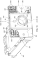
- FIG. 11 shows the substrate 900 of the current sensor 11 or 111 mounted on an electronic assembly 307, such as an inverter 10 or a controller.
- an electronic assembly 307 such as an inverter 10 or a controller.
- the current sensor e.g., 11 or 111
- its associated electromechanical assembly has a high power connector 302 or socket for receiving the conductor 16.
- the substrate 900 of the current sensor (11 or 111) is connected to or supported by the housing 304, whereas in FIG. 12 , the substrate 900 is omitted to better illustrate the connector 302.
- the connector 302 may comprise a generally cylindrical socket, for example.
- the housing 304 supports the substrate 900 in a generally perpendicular plane with respect to an axis of any conductor (16) that is inserted into or connected to the connector 302, although other mounting configurations of the substrate 900 can fall within the scope of appended claims.
- FIG. 13 illustrates the assembly 307 of FIG. 11 from a different perspective than FIG. 11 .
- FIG. 13 shows a perspective semi-exploded view of the assembly 307 where a mating portion 309 (e.g., plug) of the conductor 16 is shown as removed from the opening 903 in the ferrite structure 958 and the associated substrate 900.
- a mating portion 309 e.g., plug
- FIG. 14 is similar to FIG. 13 , except the ferrite structure 950 is replaced with dual ferrite structure 1958 and the mating portion 309 engages the connector 302.
- the mating portion 309 or plug of the conductor 16 is positioned in the connector 302.
- the conductor 16 mates with the high current connector socket of the current sensor (11 or 111).
- the dual ferrite structure 1958 comprises two ferrite members 315, where on is positioned on each side of the magnetic field sensor 20 (e.g., Hall Effect sensor). As shown, each one, of the two ferrite members 315 in FIG.
- the magnetic field sensor 20 or its inductive probe may be bounded by a ferrite member 315 on one or more sides, along a common axis 314.
- the surface-mounted, dual ferrite structure 1958 works as a magnetic flux concentrator to direct magnetic flux to the magnetic field sensor 20 (e.g., Hall Effect sensor).
- the dual ferrite structure 1958 and arrangement of FIG. 14 can achieve similar performance as a gapped torodial ferrite core. Further, the dual ferrite structure 1958 eliminates the need of a retainer 960 ( FIG.10 ) or core holder.
- the dual ferrite structure 1958 comprises a magnetic flux concentrator on either the first outer layer 807 or second outer layer 809 of substrate 900.
- the configuration of FIG. 14 uses the free volume or headroom over the power semiconductor of the inverter to make the current sensor (11 or 111) or its assembly as compact as possible. In some embodiments, only a few millimeters of clearance are needed from the closest surface of the power semiconductor package (e.g., IGBT) to inverter wall or inverter housing.
- the current sensor (e.g., 11 or 11) is capable of having a compact footprint that is smaller than many commercially available current sensors.
- the current sensor is well-suited to outperform certain commercially available current sensing schemes over a wide frequency (e.g., 0Hz to 1000Hz and beyond), an expansive current range (e.g., 0 A to approximately 500 Amps root mean squared (rms)), and a great temperature range (e.g., approximately -40 degrees Celsius to approximately 125 degrees Celsius).
- the current rating and operating range of frequency is easily scalable, particularly with scheme shown in FIG.14 .
- the magnetic field sensor 20 e.g., Hall Effect sensor
- the magnetic field sensor 20 may feature programmable sensitivity (e.g., measured in milliVolt (mV)/Gauss).
- the inductor 18 e.g., substrate-based inductor design
- the diameter of socket 302 and plug 309 can be adapted for current rating beyond 500 Amps root mean squared (rms).
- the configurations in this disclosure are well-suited for supporting a wide operating range of output frequencies of the inverter and extensive range of measured currents flowing through the conductor 16.
- This current sensor (11 or 111) does not require any potting material such as resin, silicone, polymer, or polymeric matrix; therefore, it suited for ambient storage or operation in temperature of approximately -55 degrees Celsius and below.
- the high current connector sensor (11 or 111) exhibits built-in thermal management when connector 302 or socket is placed and bolted down to power module terminals because heat loss at the connector 302 is thermally conducted to the housing 304 or its heat sink associated with the inverter (10).
- the high current connector 302 or socket makes connection to using a mating portion 309, such as a high current pin inserted into socket.
- a mating portion 309 such as a high current pin inserted into socket.
- connector 302 or socket could deploy multi-lams to make tight contact with the mating portion 309 or pin while allowing a prodigious number of paths for current that flows between the connector 302 and the mating portion 309.
- the mating portion 309 or pin is depicted in FIG.
- non-mating end of the mating portion 309 or pin is crimped with conductor 16, such as a high current cable to feeds power to load that could be away from inverter 10.
- conductor 16 such as a high current cable to feeds power to load that could be away from inverter 10.
- the connector plug 309 and socket 302 form the portion of the conductor 16 where proposed current sensing scheme resides in inverter 10 assembly.
- the ferrite structure 958 or toroidal core for use with magnetic field sensor 20 can be deleted for increased sensitivity and noise immunity for stray magnetic field.
- the deleted toroidal core is replaced by metal shield 378ing to shield against magnetic or electromagnetic fields.
- the metal shield 378ing may comprise a metal screen or one or more metal walls for mounting around a periphery of the magnetic field sensor 20 on the substrate to project perpendicularly from an outer surface of the substrate.
- windings of the inductor 18 could be wound partially or entirely on a gapped toroidal core, rather than being formed of the conductive traces and buried vias of the substrate.
- winding the inductor 18 on the toroidal core could increase cost of the assembly and raises the possibility of safety issues associated with insulation between high voltage electronics and low voltage electronics.
- the filtering circuits could be replaced with digital or advanced filtering techniques, where the filtering circuits are housed in field programmable gate array (e.g., FPGA), digital signal processor (e.g., DSP) or a microprocessor. This will increase dependency of firmware needed to implement currents sensing scheme.
- field programmable gate array e.g., FPGA
- DSP digital signal processor
- microprocessor e.g., a microprocessor
- FIG. 15 illustrates a flow chart for one embodiment of a method for sensing current. The method of FIG. 15 begins in step S1400.
- step S1400 an inductor 18 senses an alternating current signal component of an observed signal.
- Step S1400 may be carried out in accordance with various techniques, which may be applied alternately or cumulatively.
- the inductor 18 comprises a substrate, a plurality of conductive traces (e.g., buried conductive traces) associated with different layers of the substrate, and one or more conductive vias (e.g., buried vias) for interconnecting the plurality of conductive traces.
- conductive traces e.g., buried conductive traces
- conductive vias e.g., buried vias
- the inductor 18 is arranged, oriented or positioned to be proximate or near a conductor that connects an inverter output of an inverter to an electric motor.
- the conductor may intercept an opening 903 in the substrate 900 or a central region or volume of the inductor 18.
- the inductor 18 is formed by arranging the conductive traces in the different layers that are spaced apart from each other by intervening dielectric portions of a substrate wherein the conductive traces are radially extending with respect to a central axis and are limited to occupy a generally annular area or volume of the substrate.
- a magnetic field sensor 20 senses a direct current signal component of the observed signal.
- the magnetic field sensor e.g., Hall Effect sensor
- the magnetic field sensor is arranged, oriented or positioned to be proximate or near a conductor that connects an inverter output of an inverter to an electric motor.
- a first filtering circuit 26 filters the alternating current signal component with a high-pass filter response to provide a filtered alternating current signal component.
- the first filtering circuit 26 is assembled or made by mounting electronic components on one or more sides of the substrate in a region outward from an annular region or annular volume of the inductor to form at least one of a first filtering circuit, a second filtering circuit and a sensor fusion circuit on the substrate.
- a second filtering circuit 28 filters the direct current signal component with a low pass filter response to provide a filtered direct current signal component.
- the second filtering circuit 28 is assembled or made by mounting electronic components on one or more sides of the substrate in a region outward from an annular region or annular volume of the inductor to form at least one of a first filtering circuit, a second filtering circuit and a sensor fusion circuit on the substrate.
- a sensor fusion circuit 30 determines an aggregate sensed current by combining the filtered alternating current signal component and the filtered direct current signal component. For example, the sensor fusion circuit 30 scales a first gain of the filtered alternating signal component and a second gain of the filtered direct current signal component to obtain a conversion factor between actual current of the observed signal flowing through the conductor and the aggregate sensed current.
- the sensor fusion circuit 30 is assembled or made by mounting electronic components on one or more sides of the substrate in a region outward from an annular region or annular volume of the inductor to form at least one of a first filtering circuit, a second filtering circuit and a sensor fusion circuit on the substrate.
- FIG. 16 illustrates a flow chart for one embodiment of a method for sensing current. The method of FIG. 16 begins in step S1401.
- an inductor 18 senses a first alternating current signal component of an observed signal.
- the inductor 18 comprises a substrate, a plurality of conductive traces associated with different layers of the substrate, and one or more conductive vias for interconnecting the plurality of conductive traces.
- a magnetic field sensor 20 senses a direct current signal component and a second alternating signal component (e.g., a lower frequency signal component) of the observed signal, where the first alternating signal component is higher in frequency than the second alternating signal component.
- a second alternating signal component e.g., a lower frequency signal component
- a first filtering circuit 26 filters the first alternating current signal component with a high-pass filter response to provide a first filtered signal component.
- a second filtering circuit 28 filters the direct current signal component and the second alternating current signal component with a low pass filter response to provide a second filtered signal component.
- a sensor fusion circuit 30 determines an aggregate sensed current by combining the first filtered signal component and the second filtered signal component.
- additional steps may be added to the method of FIG. 15 or FIG. 16 , such as determining a change in current versus time for the alternating signal component or estimating a temperature of a conductor for carrying the observed signal.
- FIG. 17 illustrates one embodiment of a current sensor with one or more ferrite members. Like reference numbers in FIG. 17 and any other drawings in this disclosure indicate like elements.
- the current sensor comprises a multi-layered substrate 1900 that forms an inductor 18 with a central opening, a magnetic field sensor 20, one or more ferrite members, filtering circuits and a sensor fusion circuit 30.
- the central opening 903 is illustrated as substantially circular, it may be rectangular, elliptical or have any other geometric shape.
- An inductor 18 is capable of sensing an alternating current signal component of an observed signal.
- the inductor 18 comprises a multi-layered substrate 1900, a plurality of conductive traces associated with different layers of the substrate, and one or more conductive vias for interconnecting the plurality of conductive traces.
- a central opening in the multi-layered substrate 1900 and the inductor 18 has a central axis, which is coextensive with the longitudinal axis of the mating portion 309 of the conductor when in electrical and mechanical contact with connector 302.
- a magnetic field sensor 20 is adapted to sense a direct current signal component of the observed signal in a conductor associated with the current sensor.
- the magnetic field sensor 20 may comprise Hall sensor, a through-hole magnetic field sensor 20, or surface-mount integrated circuit.
- the magnetic field sensor 20 may comprise a magnetic field sensor 20 with an integral or built-in temperature sensor for sensing both the current and temperature of the conductor with the observed signal. If the magnetic field sensor 20 comprises a surface mount device instead of a through-hole device, the surface mount field sensor may be less expensive than the through-hole device and the assembly and manufacturing costs of the current sensor of the disclosure may be reduced.
- the secondary sensor 366 may comprise a second magnetic field sensor.
- the magnetic field sensors (20, 366) can be of any package type including through-hole part, surface-mount leaded part, and surface-mount lead-less package part.
- a leadless package of magnetic field sensor (20, 366) facilitates a compact layout of the circuit on the substrate (1900) or circuit board (e.g., ceramic substrate). The compact layout avoids and mitigates the circuit interaction of one or more magnetic sensors (e.g., 20, 366) with one or more stray magnetic fields or electromagnetic fields.
- the leadless surface-mount package of a magnetic sensor (e.g., 20, 366) is well-suited for dense population of the circuit board 1900 with ferrite members (362, 364) (working as a magnetic flux concentrator) leaving almost no spatial gap between magnetic sensor (20) and primary ferrite members (362), and/or magnetic sensor (366) and secondary ferrite members (364).
- a second sensor may be located below the opening in the circuit board as show, or adjacent or proximate to the magnetic field sensor 20.
- the second sensor (24 or 366) may comprise a temperature sensor, a voltage detector for detecting an excess voltage, a current change sensor, or a voltage change sensor, or a diagnostic unit.
- the diagnostic unit may detect the presence of or estimate electromagnetic interference, electromagnetic coupling, current change versus time, and voltage change versus time that might degrade the performance of the current sensor or the magnetic field sensor 20, or indicate a fault condition.
- the second sensor (24 or 366) or temperature sensor can be located in proximity to the conductor with the observed signal to determine whether a short circuit or fault results in heating of the conductor.
- the second sensor (24 or 366) may comprise a surface mount device.
- the ferrite members may comprise ferrite beads, polygonal ferrite members, rectangular ferrite members that are capable of being mounted on a substrate or printed circuit board, such as the multi-layer printed circuit board.
- the ferrite members of FIG. 17 through 22 , inclusive can replace the larger ferrite member 958 of FIG. 10 , for example.
- the ferrite members of FIG. 17 through FIG. 22 , inclusive take up less space on the surface of the circuit board than the larger ferrite member 958. Further, the ferrite members of FIG. 17 through FIG. 22 , inclusive, require no special treatment for vibration and shock.
- the ferrite members may comprise toroidal ferrite members or ferrite members of other shapes that are capable of being mounted on a substrate or printed circuit board.
- one or more primary ferrite members 362 are spaced apart radially from the magnetic field sensor 20, with respect to the longitudinal axis 369 of the conductor, on opposite sides of the magnetic field sensor 20.
- One primary ferrite member 362 is positioned coincident with a first radial axis 375 with respect to the central axis or longitudinal axis 369 of the conductor, or its mating portion 309.
- Another primary ferrite member 362 is positioned coincident with a second radial axis 376 with respect to the central axis or longitudinal axis 369 of the conductor, or its mating portion 309.
- the primary ferrite members 362 do not occupy a primary radial region 371 between the central axis (or longitudinal axis 369) and the magnetic field sensor 20.
- the primary ferrite members 362 direct, concentrate or steer an orientation of a magnetic field (e.g., magnetic flux or peak magnetic field vector) of the observed signal toward a target area or bottom surface 409 of the magnetic field sensor 20.
- a magnetic field e.g., magnetic flux or peak magnetic field vector
- the primary ferrite members 362 direct, concentrate or steer the orientation of the magnetic field of the observed signal within the primary radial area 371.
- the primary ferrite members 362 may direct the magnetic flux or orientation of the peak magnetic field perpendicular to the target area 409 or bottom surface of the magnetic field sensor 20.
- the primary ferrite members 362 enhance the magnetic field sensitivity of the magnetic field sensor 20 or allow the magnetic field sensor 20 to use a greater extent of its magnetic field sensitivity by reducing an observed noise floor.
- the ferrite members are well suited to facilitate reduced noise or greater immunity from one or more of the following: (a) change in current versus time noise (di/dt), (b) change in voltage versus time noise (di/dt), (c) electromagnetic interference, (d) electromagnetic coupling effects, and (e) stray magnetic fields from other conductors in the electronic module (e.g., inverter or controller) associated with the current sensor.
- the change in current versus time noise and the change in voltage versus time noise may be generated by the switching semiconductors of an inverter or motor controller that is used in conjunction with the current sensor or method of this disclosure.
- the electromagnetic interference, electromagnetic coupling effects and stray magnetic fields may originate from adjacent, proximate or nearby current carrying conductors, distinct from the conductor with the observed signal. Hence, the perceived sensitivity of the current sensor can be increased by using the ferrite members in accordance with this disclosure.
- the magnitude of the magnetic field sensitivity of the magnetic field sensor 20 may be measured in mV/Gauss, for instance. In one configuration, if the magnetic field sensitivity of the magnetic field sensor 20 is increased, the magnetic field sensor 20 produces an increased magnitude of its output for the same observed magnetic field strength in the conductor.
- a magnetic field sensor 20 with a lower sensitivity than otherwise possible may be used in conjunction with ferrite members.
- one or more secondary ferrite members 364 are spaced apart radially from the secondary sensor (24 or 366), with respect to the longitudinal axis 369 of the conductor, on opposite sides of the secondary sensor (24 or 366).
- One secondary ferrite member 364 is positioned coincident with a third radial axis 377 with respect to the central axis or longitudinal axis 369 of the conductor, or its mating portion 309.
- Another secondary ferrite member 364 is positioned coincident with a fourth radial axis 379 with respect to the central axis or longitudinal axis 369 of the conductor, or its mating portion 309.
- the secondary ferrite members 364 do not occupy a secondary radial region 373 between the central axis (or longitudinal axis 369) and the secondary sensor (24 or 366).
- the secondary ferrite members 364 direct, concentrate or steer an orientation of a magnetic field (e.g., magnetic flux or peak magnetic field vector) of the observed signal toward a target area or top surface 411 of the secondary sensor (24 or 366).
- a magnetic field e.g., magnetic flux or peak magnetic field vector
- the secondary ferrite members 364 direct, concentrate or steer the orientation of the magnetic field of the observed signal within the secondary radial area 373.
- the secondary ferrite members 364 may direct the magnetic flux, electromagnetic field or orientation of the peak magnetic field perpendicular to the target area 411 or top surface of the secondary sensor (24 or 366).
- the magnetic field or electrical field may be oriented toward a target area of the current change sensor as the secondary sensor (24 or 366), where the magnetic field and the electrical field are generally mutually orthogonal to each other with respect to a direction of propagation for a given electromagnetic field.
- the secondary ferrite members 364 enhance the magnetic or electrical field sensitivity of the secondary sensor (24 or 366) or allow the secondary sensor (24 or 366) to use a greater extent of its magnetic or electrical field sensitivity by reducing an observed noise floor. Accordingly, if the secondary sensor (24 or 366) comprises a current change sensor, a voltage change sensor, or an electromagnetic interference sensor the sensor may detect an electrical field, an electromagnetic field, or a magnetic field associated with the observed signal in the conductor.
- the ferrite members are well suited to facilitate reduced noise or greater immunity from one or more of the following: (a) change in current versus time noise (di/dt), (b) change in voltage versus time noise (di/dt), (c) electromagnetic interference, (d) electromagnetic coupling effects, and (e) stray magnetic fields from other conductors in the electronic module (e.g., inverter or controller) associated with the current sensor.
- the change in current versus time noise and the change in voltage versus time noise may be generated by the switching semiconductors of an inverter or motor controller that is used in conjunction with the current sensor or method of this disclosure.
- the electromagnetic interference, electromagnetic coupling effects and stray magnetic fields may originate from adjacent, proximate or nearby current carrying conductors, distinct from the conductor with the observed signal.
- the perceived sensitivity of the secondary sensor (24 or 366) and the overall current sensor can be increased by using the ferrite members in accordance with this disclosure.
- a first filtering circuit 26 has a high-pass filter response.
- the first filtering circuit 26 is coupled to the inductor 18 to provide a filtered alternating current signal component.
- the inductor 18, along with first filtering circuit 26, is used to measure the current change and also a higher frequency (e.g., at or above 1000Hz) time varying current of any wave-shape, such as, sinusoidal, trapezoidal, square, or otherwise.
- a second filtering circuit 28 has a low-pass filter response.
- the second filtering circuit 28 is coupled to the magnetic field sensor 20 to provide a filtered direct current signal component.
- the magnetic field sensors 20 along with associated electronic circuits are used to measure the current signal from 0.0 Hz (DC) to a lower frequency (e.g., about 1000 Hz or 1500 Hz) time varying current of any wave-shape, such as, sinusoidal, trapezoidal, square, or otherwise.
- a sensor fusion circuit 30 is adapted to accept the filtered alternating current signal component and the filtered direct current signal component and to determine an aggregate sensed current.
- the primary ferrite members 362 are grounded with one or more conductors (e.g., threaded through the primary ferrite members 362, wrapped around the primary ferrite members 362, or otherwise configured) to suppress electromagnetic interference with respect to the magnetic field sensor 20.
- the secondary ferrite members 364 are grounded with one or more conductors (e.g., threaded through the secondary ferrite members 362, wrapped around the secondary ferrite members 362, or otherwise configured) to suppress electromagnetic interference with respect to the magnetic field sensor 20, the secondary sensor (24 or 366), or both.
- the inductor 18 and the magnetic field sensor 20 are arranged to be proximate or near a conductor that connects an inverter output of an inverter to an electric motor.
- an optional temperature sensor is spaced apart from the conductor to estimate a temperature of the conductor.
- FIG. 18 is similar to the current sensor of FIG. 17 , except FIG. 18 deletes the ferrite members (362, 364) and designates the multi-layered substrate 1901 without the ferrite members (362, 364).
- the multi-layered substrate 1901 provides illustrated examples of through-holes 376 for mounting the ferrite members (362, 364), other embodiments that fall within the scope of the claims do not require any through-holes for mounting the ferrite members (362, 364).
- Like reference numbers in FIG. 17 and FIG. 18 and in any other drawings, indicate like elements.
- the current sensor of FIG. 18 may be used in conjunction with a metal shield 378 as shown in FIG. 19 or FIG. 20 , for example.
- FIG. 19 is similar to the current sensor of FIG. 17 or FIG. 18 , except FIG. 19 adds a metal or metallic shield.
- the metal shield 378 or metallic shield comprises a generally rectangular hollow body with a cylindrical portion 381 about a central axis (or longitudinal axis 369) and a perimeter 386.
- the cylindrical portion 381 may contain a primary opening 380 and a secondary opening 382, where the primary opening 381 is aligned with the primary radial region 371 (or a target area 409 of the magnetic field sensor 20) and wherein the secondary opening 382 is aligned with the secondary radial region 373 (or a target area 411 of the secondary sensor (24 or 366)).
- the perimeter may comprise one or more perimeter walls 381.
- the metal shield 378 is stamped, formed, welded, cast or otherwise constructed from steel or a ferromagnetic alloy.
- the metal shield 378 may be formed as a metal screen or an insulting screen with conductive metallic particles adhesively bonded thereto.
- the metal or metallic shield is formed of metallic particles bound in a polymer matrix, plastic matrix, or resin.
- the magnetic shield is mounted to a side of the multi-layered substrate (1900 or 1901), the hollow body comprising a recess to receive and cover any components mounted on the side of the multi-layered substrate (1900 or 1901).
- a metal shield 378 or metallic shield has a recess for enclosing at least an annular region (e.g., a region with a substantially circular inner boundary and a substantially circular, elliptical curved, or rectangular outer boundary or perimeter) extending outward around the opening and covers the magnetic field sensor 20 to reduce, attenuate or minimize one or more stray magnetic fields not associated with the observed signal in the conductor.
- annular region e.g., a region with a substantially circular inner boundary and a substantially circular, elliptical curved, or rectangular outer boundary or perimeter
- the outer perimeter 386 of the metal shield metallic shield may terminate in a substantially rectangular, substantially polygonal, or substantially rectilinear outer boundary.
- the metal shield 378 is well suited for improving the current sensor's and the magnetic field sensor's immunity to one or more of the following: electromagnetic noise, electromagnetic interference, and stray magnetic fields, for example.
- a metal shield 378 or metallic shield encloses an annular region extending outward around the opening and covers the current change sensor.
- the metal shield 378 has a primary opening 380, in an inner cylindrical surface 381, facing the magnetic field sensor 20 and the primary radial region 371; the metal shield 378 and a secondary opening 382, in the inner cylindrical surface 381, facing the secondary sensor or current change sensor and the secondary radial region 373.
- the inner cylindrical surface 381 comprises a substantially cylindrical surface or an interior surface with the primary opening 380 for receiving a steered, directed or otherwise concentrated magnetic field, where the concentrated magnetic field is associated with the observed signal and emanates (e.g., radiates) from the conductor toward the target area of the magnetic field sensor 20.
- the metal shield 378 has a primary opening 380 facing the magnetic field sensor 20 in the primary radial region 371 facing the magnetic field sensor 20 to reduce one or more stray magnetic fields not associated with the observed signal, while allowing the observed signal to be measured by the magnetic field sensor 20.
- the perimeter 386 of metal shield 378 is grounded to ensure that shield body remains substantially at ground potential.
- the ground ensures that the metal shield 378 doesn't develop any appreciable voltage on it as compared to system (inverter) ground, chassis ground, vehicle ground or vehicle battery ground.
- a metal shield 378 is placed over the magnetic sensor 20 or magnetic sensors 20 with a hole in the metal shield 378 for the current conductor pass through.
- the metal shield 378 comprises a generally hollow body mounted to a side of the multi-layered substrate (1900 or 1901) to form a recess to receive and cover the magnetic sensor 20, the secondary sensor (24 or 366), the primary ferrite members 362 and the secondary ferrite members 364 mounted on the side 807 of the multi-layered substrate 1900 of FIG. 17 .
- the metal shield 378 extends outward around the central opening 903 and covers the magnetic field sensor 20 and primary ferrite members 362.
- the metal shield 378 extends outward around the central opening 903 and covers the secondary sensor (24 or 366) and secondary ferrite members 364.
- the metal shield 378 comprises a generally hollow body mounted to a side of the multi-layered substrate 1901 to form a barrier to stray magnetic fields from other sources that might otherwise interfere with the electrical field, magnetic field or electromagnetic field, sensed or attempted to be sensed by the magnetic field sensor 20, the secondary sensor (24 or 366), or both.
- FIG. 20 is similar to the current sensor of FIG. 17 or FIG. 18 , except FIG. 20 adds a metal shield 478.
- Like reference numbers indicate like elements in FIG. 17 through FIG. 20 , inclusive an in any other drawings presented in this disclosure.
- the metal shield 478 or metallic shield encloses an annular region extending outward around the opening and covers the magnetic field sensor 20 and the secondary sensor (24 or 366).
- the magnetic field sensor 20 and the secondary sensor (24 or 366) are shown in phantom with dashed lines because they underneath the metal shield 478.
- the metal shield 478 or metallic shield comprises a generally cylindrical, curved, circular or elliptical hollow body with a cylindrical portion 381 about a central axis (or longitudinal axis 369) and a perimeter 386.
- the cylindrical portion 381 may contain a primary opening 380 and a secondary opening 382, where the primary opening 381 is aligned with the primary radial region 371 (or a target area 409 of the magnetic field sensor 20) and wherein the secondary opening 382 is aligned with the secondary radial region 373 (or a target area 411 of the secondary sensor (24 or 366)).
- the metallic shield has a first opening, in an inner cylindrical surface, facing the magnetic field sensor 20 and a second opening, in the inner cylindrical surface, facing the current change sensor in secondary radial region 373.
- the perimeter may comprise a perimeter wall 384 or perimeter boundary.
- the outer perimeter wall 384 of the metal shield or metallic shield may terminate in a substantially substantially cylindrical, curved, circular, or elliptical outer boundary.
- the metal shield 478 is stamped, formed, welded, cast or otherwise constructed from steel or a ferromagnetic alloy.
- the metal shield 478 may be formed as a metal screen or an insulting screen with conductive metallic particles adhesively bonded thereto.
- the metal shield 478 or metallic shield is formed of metallic particles bound in a polymer matrix, plastic matrix, or resin.
- the metal shield 478 has a first opening facing the magnetic field sensor 20 in the primary radial region 371 facing the magnetic field sensor 20 to reduce one or more stray magnetic fields not associated with the observed signal, while allowing the observed signal to be measured by the magnetic field sensor 20.
- the metal shield 478 comprises a generally annular hollow body; the generally annular hollow body is mounted to a side 807 of the multi-layered substrate 1900 to form a recess to receive and cover the magnetic field sensor 20, the secondary sensor (24 or 366), the primary ferrite members 262 and the secondary ferrite members 264 mounted on the side 807 of the multi-layered substrate 1900.
- the metal shield 478 comprises a generally annular hollow body; the generally annular hollow body is mounted to a side 807 of the multi-layered substrate 1901 to form a barrier to stray electrical fields, magnetic fields, or electromagnetic fields from other sources that might otherwise interfere with magnetic field sensed or attempted to be sensed by the magnetic field sensor 20, the secondary sensor (24 or 366), or both.
- step S350 The method of FIG. 21 starts in step S350.
- one or more ferrite members (362, 364) concentrate a magnetic field (e.g., magnetic flux or magnetic field vector) of an observed signal toward a target area 409 of a magnetic field sensor 20.
- ferrite members (362, 364) and a magnetic field sensor 20 are mounted on a circuit board 1900 in a plane that is substantially perpendicular to a longitudinal axis 369 of a conductor (309) conducting a signal to be measured, where the ferrite members (362, 364) are spaced apart radially from opposite sides of the magnetic field sensor 20.
- the magnetic field sensor 20 may have a target area 409 that is more sensitive to detection and measurement of a sensed magnetic field than other portions of the magnetic field sensor 20.
- one or more primary ferrite members 362 concentrate a magnetic field (e.g., magnetic flux or magnetic field vector) of an observed signal toward a target area 409 of a magnetic field sensor 20; one or more secondary ferrite members 364 concentrate an electromagnetic, electrical or magnetic field (e.g., magnetic flux or magnetic field vector) of an observed signal toward a target area 411 of a secondary sensor (24 or 366.) Further, the secondary sensor 24 may provide input to the first filtering circuit 26 as previously discussed in FIG. 1 , for example.
- a magnetic field e.g., magnetic flux or magnetic field vector
- the secondary sensor 24 may provide input to the first filtering circuit 26 as previously discussed in FIG. 1 , for example.
- a magnetic field sensor 20 senses a direct current signal component or a lower frequency alternating current signal component of the observed signal with the concentrated magnetic field. For instance, the concentrated magnetic field was directed, steered or concentrated in accordance with step S350 such that the magnetic field impinges upon or intercepts a target area 409 of the magnetic field sensor 20.
- an inductor 18 senses an alternating current signal component (e.g., higher frequency alternating signal component) of the observed signal.
- the inductor 18 comprises a substrate, conductive traces associated with different layers of the substrate, and one or more conductive vias for interconnecting the plurality of conductive traces.
- a first filtering circuit 26 filters the alternating current signal component with a high-pass filter response to provide a filtered alternating current signal component.
- a second filtering circuit 28 filters the direct current signal component (or the low frequency alternating current signal component) with a low pass filter response to provide a filtered direct current signal component.
- step S360 sensor fusion circuit 30 determines an aggregate sensed current by combining the filtered alternating current signal component and the filtered direct current signal component.
- FIG. 22 starts in step S351.
- Like reference numbers in FIG. 21 and FIG. 22 indicate like steps or procedures.
- a metal shield (378 or 478) or metallic shield shields a magnetic field sensor 20 or its target area (409) from stray magnetic field.
- the stray magnetic field is not the desired magnetic field associated with the signal to be measured in the conductor, or its mating portion 309.
- the desired magnetic field is oriented such that the magnetic flux or magnetic field vector of the observed signal is oriented toward the target area of the magnetic field sensor 20.
- metal shield (378 or 478) and a magnetic field sensor 20 are mounted on a circuit board (1900 or 1901) in a plane that is substantially perpendicular to a longitudinal axis 369 of a conductor conducting a signal to be measured, where metal shield (378 or 478) covers or surrounds the magnetic field sensor 20, except for an opening (e.g., primary opening 380) for receiving a radially oriented magnetic field from the signal to be measured in the conductor.
- the primary opening 380 in the cylindrical surface 381 of the metal shield (378 or 478) may be aligned with the target area 409 of the magnetic field sensor 20.
- the magnetic field sensor 20 may have a target area 409 that is more sensitive to detection and measurement of a sensed magnetic field than other portions of the magnetic field sensor 20.
- a magnetic field sensor 20 senses a direct current signal component or a lower frequency alternating current signal component of the observed signal that is shielded from the stray magnetic field (e.g., in step S351).
- Step S353 may be carried out in accordance with various techniques that may be applied alternately or cumulatively.
- the magnetic field sensor 20 senses a direct current signal component or a lower frequency alternating current signal component of the observed signal that is shielded from the stray magnetic field by a metal shield (378 or 478).
- the magnetic field sensor 20 senses a direct current signal component or a lower frequency alternating current signal component of the observed signal that is shielded from the stray magnetic field by a metal shield (378 or 478); where the metal shield comprises a cylindrical inner surface 381 with a primary opening 380 for receiving the magnetic field associated with the observed signal that emanates or radiates from the conductor or its mating portion (309).
- a magnetic field sensor 20 senses a direct current signal component or a lower frequency alternating current signal component of the observed signal with a steered or concentrated magnetic field.
- the concentrated magnetic field was directed, steered or concentrated in accordance with step S350 of FIG. 21 such that the magnetic field impinges upon or intercepts a target area 409 of the magnetic field sensor 20.
- an inductor 18 senses an alternating current signal component (e.g., higher frequency alternating signal component) of the observed signal.
- the inductor comprises a substrate, conductive traces associated with different layers of the substrate, and one or more conductive vias for interconnecting the plurality of conductive traces.
- a first filtering circuit 26 filters the alternating current signal component with a high-pass filter response to provide a filtered alternating current signal component.
- a second filtering circuit 28 filters the direct current signal component (or direct current signal component and the low frequency alternating current signal component) with a low pass filter response to provide a filtered direct current signal component.
- step S360 sensor fusion circuit 30 determines an aggregate sensed current by combining the filtered alternating current signal component and the filtered direct current signal component.
Landscapes
- Physics & Mathematics (AREA)
- General Physics & Mathematics (AREA)
- Engineering & Computer Science (AREA)
- Power Engineering (AREA)
- Measuring Instrument Details And Bridges, And Automatic Balancing Devices (AREA)
- Inverter Devices (AREA)
Claims (15)
- Stromsensor, der Folgendes beinhaltet:eine Spule (18), die zum Erfassen einer Wechselstromsignalkomponente eines beobachteten Signals konfiguriert ist;eine zentrale Öffnung (903) in einem mehrschichtigen Träger mit einer zentralen Achse;einen Magnetfeldsensor (20), der zum Erfassen einer Gleichstromsignalkomponente des beobachteten Signals konfiguriert ist;mehrere primäre Ferritglieder (315), die auf entgegengesetzten Seiten des Magnetfeldsensors vom Magnetfeldsensor beabstandet sind, um eine Ausrichtung eines Magnetfelds des beobachteten Signals auf einen Zielbereich des Magnetfeldsensors zu konzentrieren oder zu lenken;eine erste Filterschaltung (26) mit einem Hochpassfilterverhalten, wobei die erste Filterschaltung mit der Spule gekoppelt ist, um eine gefilterte Wechselstromsignalkomponente bereitzustellen;eine zweite Filterschaltung (28) mit einem Tiefpassfilterverhalten, wobei die zweite Filterschaltung mit dem Magnetfeldsensor gekoppelt ist, um eine gefilterte Gleichstromsignalkomponente bereitzustellen; undeine Sensorfusionsschaltung (30), die zum Annehmen der gefilterten Wechselstromsignalkomponente und der gefilterten Gleichstromsignalkomponente und zum Bestimmen eines aggregierten erfassten Stroms konfiguriert ist.
- Stromsensor nach Anspruch 1, wobei die primären Ferritelemente geerdet sind, um elektromagnetische Störungen in Bezug auf den Magnetfeldsensor zu unterdrücken.
- Stromsensor nach Anspruch 1, der ferner Folgendes beinhaltet:
einen Leiter, wobei die Spule und der Magnetfeldsensor so angeordnet sind, dass sie neben dem oder in der Nähe des Leiter(s) sind, der einen Umrichterausgang eines Umrichters mit einem Elektromotor verbindet. - Stromsensor nach Anspruch 1, der ferner Folgendes beinhaltet:
einen Metallschirm, der sich nach außen um die zentrale Öffnung erstreckt und den Magnetfeldsensor und die primären Ferritelemente abdeckt. - Stromsensor nach Anspruch 4, wobei der Metallschirm einen im Wesentlichen zylindrischen Teil mit einer primären Öffnung zur Aufnahme des konzentrierten Magnetfelds beinhaltet, das mit dem beobachteten Signal assoziiert ist und von einem Leiter in Richtung auf den Zielbereich des Magnetfeldsensors ausgeht.
- Stromsensor nach Anspruch 1, der ferner Folgendes beinhaltet:einen Leiter, wobei die Spule und der Magnetfeldsensor angeordnet sind, um neben dem oder in der Nähe des Leiter(s) angeordnet zu sein, der einen Umrichterausgang eines Umrichters mit einem Elektromotor verbindet; undeinen Stromänderungssensor, der vom Leiter beabstandet ist, zum Schätzen einer Veränderung des Stroms im Leiter.
- Stromsensor nach Anspruch 6, der ferner Folgendes beinhaltet:
mehrere sekundäre Ferritelemente, die auf entgegengesetzten Seiten des Stromänderungssensors vom Stromänderungssensor beabstandet sind, wobei die sekundären Ferritelemente ein Elektromagnetfeld in einer sekundären radialen Region zwischen der Mittelachse und dem Stromänderungssensor und in Richtung auf einen Zielbereich des Stromänderungssensors konzentrieren oder lenken. - Stromsensor nach Anspruch 7, der ferner einen Metallschirm beinhaltet, der sich nach außen um die zentrale Öffnung erstreckt und den Stromänderungssensor und die sekundären Ferritelemente abdeckt.
- Stromsensor nach Anspruch 8, wobei der Metallschirm einen im Wesentlichen zylindrischen Teil mit einer sekundären Öffnung beinhaltet, die dem Zielbereich des Stromänderungssensors gegenüberliegt, zum Aufnehmen eines Elektromagnetfelds, das mit dem beobachteten Signal assoziiert ist und von einem Leiter ausgeht.
- Stromsensor nach Anspruch 7, wobei die sekundären Ferritelemente geerdet sind, um elektromagnetische Störungen in Bezug auf den Stromänderungssensor zu unterdrücken.
- Stromsensor nach Anspruch 1, wobei ein metallischer Schirm eine ringförmige Region umschließt, die sich nach außen um die Öffnung erstreckt und den Magnetfeldsensor abdeckt, um ein oder mehr nicht mit dem beobachteten Signal assoziierte Streumagnetfelder zu reduzieren.
- Stromsensor nach Anspruch 1, wobei der metallische Schirm eine erste Öffnung in einer primären radialen Region beinhaltet, die einem Zielbereich des Magnetfeldsensors gegenüberliegt, um ein oder mehr nicht mit dem beobachteten Signal assoziierte Streumagnetfelder zu reduzieren.
- Stromsensor nach Anspruch 1, wobei der magnetische Schirm einen allgemein ringförmigen Hohlkörper beinhaltet, der an einer Seite des mehrschichtigen Trägers montiert ist, wobei der Hohlkörper eine Aussparung zum Aufnehmen und Abdecken des Magnetfeldsensors und der primären Ferritelemente, die auf der Seite des mehrschichtigen Trägers montiert sind, beinhaltet.
- Stromsensor nach Anspruch 1, wobei der magnetische Schirm einen allgemein rechteckigen Hohlkörper mit einem zylindrischen Teil um eine Mittelachse beinhaltet, bei dem der magnetische Schirm an einer Seite des mehrschichtigen Trägers montiert ist, wobei der Hohlkörper eine Aussparung zum Aufnehmen und Abdecken des Magnetfeldsensors und der primären Ferritelemente, die auf der Seite des mehrschichtigen Trägers montiert sind, beinhaltet.
- Stromsensor nach Anspruch 1, wobei die Spule einen mehrschichtigen Träger, mehrere mit verschiedenen Schichten des Trägers verbundene Leiterbahnen und ein oder mehr leitfähige Durchkontaktierungen zur Verbindung der mehreren Leiterbahnen beinhaltet.
Applications Claiming Priority (3)
| Application Number | Priority Date | Filing Date | Title |
|---|---|---|---|
| US13/790,835 US9410990B2 (en) | 2013-03-08 | 2013-03-08 | Method and sensor for sensing current in a conductor |
| US13/930,940 US9297836B2 (en) | 2013-03-08 | 2013-06-28 | Method and sensor for sensing current in a conductor |
| PCT/US2013/074275 WO2014137433A1 (en) | 2013-03-08 | 2013-12-11 | Sensing electrical current in a conductor |
Publications (3)
| Publication Number | Publication Date |
|---|---|
| EP2965105A1 EP2965105A1 (de) | 2016-01-13 |
| EP2965105A4 EP2965105A4 (de) | 2016-11-23 |
| EP2965105B1 true EP2965105B1 (de) | 2023-09-27 |
Family
ID=51487068
Family Applications (1)
| Application Number | Title | Priority Date | Filing Date |
|---|---|---|---|
| EP13876874.2A Active EP2965105B1 (de) | 2013-03-08 | 2013-12-11 | Messung des elektrischen stroms in einem leiter |
Country Status (5)
| Country | Link |
|---|---|
| US (1) | US9297836B2 (de) |
| EP (1) | EP2965105B1 (de) |
| CN (1) | CN105026946B (de) |
| BR (1) | BR112015018451B1 (de) |
| WO (1) | WO2014137433A1 (de) |
Families Citing this family (28)
| Publication number | Priority date | Publication date | Assignee | Title |
|---|---|---|---|---|
| US9054515B2 (en) * | 2013-06-12 | 2015-06-09 | Infineon Technologies Austria Ag | Current measurement and overcurrent detection |
| DE102014208680A1 (de) * | 2014-05-08 | 2015-11-12 | Robert Bosch Gmbh | Verfahren zur Überwachung von Stromsensoren |
| US10097130B2 (en) * | 2015-12-02 | 2018-10-09 | Aisin Seiki Kabushiki Kaisha | Energization control system and sensor unit |
| WO2017149359A1 (en) * | 2016-03-03 | 2017-09-08 | Kongsberg Inc. | Circuit and method for shunt current sensing |
| DE102016107798B4 (de) * | 2016-04-27 | 2020-12-10 | Infineon Technologies Ag | Kompakte Sensorpackung |
| DE102016113126A1 (de) * | 2016-07-15 | 2018-01-18 | Tdk-Micronas Gmbh | Verfahren zur Berechnung der Phasenverschiebung oder Amplitude eines Drei-Phasen-Systems |
| US9912266B2 (en) | 2016-08-02 | 2018-03-06 | Otis Elevator Company | Motor torque ripple reduction using DC bus harmonics |
| US9979320B2 (en) * | 2016-08-26 | 2018-05-22 | Deere & Company | Electronic inverter assembly |
| TWI629486B (zh) | 2016-09-14 | 2018-07-11 | 台達電子工業股份有限公司 | 電流偵測裝置及其操作方法 |
| US11293949B2 (en) * | 2017-06-14 | 2022-04-05 | Mitsubishi Electric Corporation | Current detection apparatus and power conversion apparatus |
| EP3496118A1 (de) | 2017-12-07 | 2019-06-12 | Koninklijke Philips N.V. | Luftkerninduktoranordnung |
| US10354462B1 (en) * | 2018-04-06 | 2019-07-16 | Toyota Motor Engineering & Manufacturing North America, Inc. | Fault diagnosis in power electronics using adaptive PCA |
| DE102018109878A1 (de) * | 2018-04-24 | 2019-10-24 | Elpro Gmbh | Verfahren zur Herstellung einer Luftspule |
| DE102018109876A1 (de) * | 2018-04-24 | 2019-10-24 | Elpro Gmbh | Luftspule |
| US10557875B2 (en) * | 2018-05-09 | 2020-02-11 | Fluke Corporation | Multi-sensor scanner configuration for non-contact voltage measurement devices |
| DE102019200333A1 (de) * | 2019-01-14 | 2020-07-16 | Phoenix Contact Gmbh & Co. Kg | Mess-System zur Erfassung von Störungen auf Leitungen eines Gerätes oder einer Anlage |
| DE102019102567B3 (de) * | 2019-02-01 | 2020-03-05 | Dr. Ing. H.C. F. Porsche Aktiengesellschaft | Sensorvorrichtung zur Messung von Gleich- und Wechselströmen |
| JP7370164B2 (ja) | 2019-04-23 | 2023-10-27 | 富士電機メーター株式会社 | 電流センサ及び電力量計 |
| JP7430989B2 (ja) | 2019-06-20 | 2024-02-14 | 横河電機株式会社 | 電流測定装置 |
| DE102019120666B3 (de) * | 2019-07-31 | 2020-10-29 | Dr. Ing. H.C. F. Porsche Aktiengesellschaft | Sensorvorrichtung zur breitbandigen Messung von elektrischen Strömen durch einen Leiter und Verfahren zur breitbandigen Messung |
| US11363746B2 (en) * | 2019-09-06 | 2022-06-14 | Teradyne, Inc. | EMI shielding for a signal trace |
| FR3108986B1 (fr) * | 2020-04-02 | 2022-04-15 | Safran Electrical & Power | Capteur de courant à très large bande passante |
| DE102021207128A1 (de) | 2021-07-07 | 2023-01-12 | Zf Friedrichshafen Ag | Elektrische Einrichtung für ein Kraftfahrzeug |
| TWI769049B (zh) * | 2021-08-11 | 2022-06-21 | 威剛科技股份有限公司 | 電流感測模組 |
| EP4206694A1 (de) * | 2022-01-03 | 2023-07-05 | ABB Schweiz AG | Signalvereinigungseinheit mit einstellbarer zeitkonstante |
| WO2023158760A1 (en) * | 2022-02-16 | 2023-08-24 | The University Of North Carolina At Charlotte | Switch current sensors |
| US20240055998A1 (en) * | 2022-08-11 | 2024-02-15 | Delta Electronics, Inc. | Photovoltaic inverter |
| CN115183897A (zh) * | 2022-09-09 | 2022-10-14 | 之江实验室 | 一种基于高频交流信号的温度测量系统及方法 |
Citations (3)
| Publication number | Priority date | Publication date | Assignee | Title |
|---|---|---|---|---|
| US7358724B2 (en) * | 2005-05-16 | 2008-04-15 | Allegro Microsystems, Inc. | Integrated magnetic flux concentrator |
| US20110050382A1 (en) * | 2009-08-25 | 2011-03-03 | Access Business Group International Llc | Flux concentrator and method of making a magnetic flux concentrator |
| US20130134970A1 (en) * | 2010-01-29 | 2013-05-30 | Commissariat A L'energie Atomique Et Aux Energies Alternatives | Integrated Magnetometer and its Manufacturing Process |
Family Cites Families (19)
| Publication number | Priority date | Publication date | Assignee | Title |
|---|---|---|---|---|
| DE1489742A1 (de) | 1964-05-18 | 1969-04-03 | Ceskoslovenska Akademie Ved | Schaltungsanordnung eines Superstabilisators eines magnetischen Feldes |
| FR2678069A1 (fr) * | 1991-06-18 | 1992-12-24 | Commissariat Energie Atomique | Capteur de courant utilisant un magnetometre directionnel a resonance. |
| JP3542197B2 (ja) | 1995-04-28 | 2004-07-14 | 本田技研工業株式会社 | 電動車両の制御装置 |
| US5615075A (en) | 1995-05-30 | 1997-03-25 | General Electric Company | AC/DC current sensor for a circuit breaker |
| EP1012609B1 (de) * | 1997-04-21 | 2001-10-24 | Arbeitsgemeinschaft Prof. Dr. J. Hugel | Gerät mit bandpass grosser bandbreite zum messen elektrischer stromstärke in einem leiter |
| US6426617B1 (en) | 1999-09-28 | 2002-07-30 | Rockwell Automation Technologies, Inc. | Hall effect current sensor system packaging |
| US6445171B2 (en) * | 1999-10-29 | 2002-09-03 | Honeywell Inc. | Closed-loop magnetoresistive current sensor system having active offset nulling |
| US6564084B2 (en) | 2001-03-02 | 2003-05-13 | Draeger Medical, Inc. | Magnetic field shielding and detecting device and method thereof |
| JP4332623B2 (ja) * | 2003-02-26 | 2009-09-16 | テクトロニクス・インコーポレイテッド | 電流プローブ |
| US7164263B2 (en) | 2004-01-16 | 2007-01-16 | Fieldmetrics, Inc. | Current sensor |
| US7218095B2 (en) | 2004-07-30 | 2007-05-15 | Verigy (Singapore) Pte. Ltd. | Method and apparatus for electromagnetic interference shielding in an automated test system |
| JP4916807B2 (ja) | 2006-01-30 | 2012-04-18 | 株式会社ダイヘン | 電圧検出用プリント基板及びそれを用いた電圧検出器 |
| US7309980B2 (en) * | 2006-05-08 | 2007-12-18 | Tektronix, Inc. | Current sensing circuit for use in a current measurement probe |
| US7605580B2 (en) * | 2007-06-29 | 2009-10-20 | Infineon Technologies Austria Ag | Integrated hybrid current sensor |
| US8253414B2 (en) * | 2007-12-27 | 2012-08-28 | Infineon Technologies Ag | Integrated circuit including a magnetic field sensitive element and a coil |
| IT1392716B1 (it) | 2009-01-13 | 2012-03-16 | Seneca S R L | Metodo di misura di una corrente elettrica |
| US8258777B2 (en) | 2009-09-04 | 2012-09-04 | Weihua Chen | Inductive proximity sensor |
| US8395381B2 (en) | 2010-07-09 | 2013-03-12 | Invensense, Inc. | Micromachined magnetic field sensors |
| US20130027021A1 (en) * | 2011-07-28 | 2013-01-31 | Abb Inc. | Current sensor |
-
2013
- 2013-06-28 US US13/930,940 patent/US9297836B2/en active Active
- 2013-12-11 BR BR112015018451-0A patent/BR112015018451B1/pt active IP Right Grant
- 2013-12-11 WO PCT/US2013/074275 patent/WO2014137433A1/en active Application Filing
- 2013-12-11 CN CN201380074268.3A patent/CN105026946B/zh active Active
- 2013-12-11 EP EP13876874.2A patent/EP2965105B1/de active Active
Patent Citations (3)
| Publication number | Priority date | Publication date | Assignee | Title |
|---|---|---|---|---|
| US7358724B2 (en) * | 2005-05-16 | 2008-04-15 | Allegro Microsystems, Inc. | Integrated magnetic flux concentrator |
| US20110050382A1 (en) * | 2009-08-25 | 2011-03-03 | Access Business Group International Llc | Flux concentrator and method of making a magnetic flux concentrator |
| US20130134970A1 (en) * | 2010-01-29 | 2013-05-30 | Commissariat A L'energie Atomique Et Aux Energies Alternatives | Integrated Magnetometer and its Manufacturing Process |
Also Published As
| Publication number | Publication date |
|---|---|
| BR112015018451A2 (pt) | 2017-07-18 |
| EP2965105A4 (de) | 2016-11-23 |
| CN105026946B (zh) | 2018-09-14 |
| US20140253109A1 (en) | 2014-09-11 |
| CN105026946A (zh) | 2015-11-04 |
| EP2965105A1 (de) | 2016-01-13 |
| BR112015018451B1 (pt) | 2021-12-21 |
| US9297836B2 (en) | 2016-03-29 |
| WO2014137433A1 (en) | 2014-09-12 |
Similar Documents
| Publication | Publication Date | Title |
|---|---|---|
| EP2965105B1 (de) | Messung des elektrischen stroms in einem leiter | |
| EP2965096B1 (de) | Verfahren zur messung von strom in einem leiter | |
| EP1965217B1 (de) | Stromsensor mit offenem Regelkreis und hoher Bandbreite | |
| JP6477089B2 (ja) | 電流センサ付バスバーモジュール | |
| US7728578B2 (en) | Method and apparatus for high current measurement | |
| US20090027047A1 (en) | Current sensor having sandwiched magnetic permeability layer | |
| US20200300894A1 (en) | Current sensor assembly | |
| JP2007225588A (ja) | 電流検出用プリント基板、電圧検出用プリント基板及びそれらを用いた電流・電圧検出器、並びに電流検出器及び電圧検出器 | |
| US20200132725A1 (en) | A combination current sensing device | |
| JP7216730B2 (ja) | 空芯インダクタアセンブリ | |
| WO2015075623A1 (en) | Power module comprising an integrated current measurement | |
| US20220026469A1 (en) | Current sensing device having an integrated electrical shield | |
| US11493537B2 (en) | Magnetic field-based current sensor for frequency-compensated measurement of alternating currents | |
| JP6938666B2 (ja) | 集積電子機器を有するブッシング | |
| JP6914395B1 (ja) | 電力変換装置 | |
| Sirat | Ultra-Wideband Contactless Current Sensors for Power Electronics Applications | |
| KR101913143B1 (ko) | 전류 통과부에서 전류를 측정하기 위한 장치 | |
| JP5777258B2 (ja) | 高電力用可変インダクタとこれを用いたフィルタ | |
| JP2009210496A (ja) | 電流センサ | |
| KR20140128154A (ko) | 전자파 내성이 강화된 전류 센서 |
Legal Events
| Date | Code | Title | Description |
|---|---|---|---|
| PUAI | Public reference made under article 153(3) epc to a published international application that has entered the european phase |
Free format text: ORIGINAL CODE: 0009012 |
|
| STAA | Information on the status of an ep patent application or granted ep patent |
Free format text: STATUS: REQUEST FOR EXAMINATION WAS MADE |
|
| 17P | Request for examination filed |
Effective date: 20151002 |
|
| AK | Designated contracting states |
Kind code of ref document: A1 Designated state(s): AL AT BE BG CH CY CZ DE DK EE ES FI FR GB GR HR HU IE IS IT LI LT LU LV MC MK MT NL NO PL PT RO RS SE SI SK SM TR |
|
| AX | Request for extension of the european patent |
Extension state: BA ME |
|
| RIN1 | Information on inventor provided before grant (corrected) |
Inventor name: FISK, ARON Inventor name: SINGH, BRIJ, N. Inventor name: CLEMENTS, NEAL, D. Inventor name: WIELAND, ANDREW, D. |
|
| DAX | Request for extension of the european patent (deleted) | ||
| A4 | Supplementary search report drawn up and despatched |
Effective date: 20161026 |
|
| RIC1 | Information provided on ipc code assigned before grant |
Ipc: G01R 15/20 20060101ALI20161020BHEP Ipc: G01R 15/00 20060101ALI20161020BHEP Ipc: G01R 15/18 20060101ALI20161020BHEP Ipc: G01R 33/00 20060101AFI20161020BHEP Ipc: G01R 19/00 20060101ALI20161020BHEP Ipc: G01R 31/42 20060101ALI20161020BHEP |
|
| STAA | Information on the status of an ep patent application or granted ep patent |
Free format text: STATUS: EXAMINATION IS IN PROGRESS |
|
| 17Q | First examination report despatched |
Effective date: 20210412 |
|
| STAA | Information on the status of an ep patent application or granted ep patent |
Free format text: STATUS: EXAMINATION IS IN PROGRESS |
|
| GRAP | Despatch of communication of intention to grant a patent |
Free format text: ORIGINAL CODE: EPIDOSNIGR1 |
|
| STAA | Information on the status of an ep patent application or granted ep patent |
Free format text: STATUS: GRANT OF PATENT IS INTENDED |
|
| INTG | Intention to grant announced |
Effective date: 20230424 |
|
| GRAS | Grant fee paid |
Free format text: ORIGINAL CODE: EPIDOSNIGR3 |
|
| GRAA | (expected) grant |
Free format text: ORIGINAL CODE: 0009210 |
|
| STAA | Information on the status of an ep patent application or granted ep patent |
Free format text: STATUS: THE PATENT HAS BEEN GRANTED |
|
| AK | Designated contracting states |
Kind code of ref document: B1 Designated state(s): AL AT BE BG CH CY CZ DE DK EE ES FI FR GB GR HR HU IE IS IT LI LT LU LV MC MK MT NL NO PL PT RO RS SE SI SK SM TR |
|
| REG | Reference to a national code |
Ref country code: GB Ref legal event code: FG4D |
|
| REG | Reference to a national code |
Ref country code: CH Ref legal event code: EP |
|
| REG | Reference to a national code |
Ref country code: DE Ref legal event code: R096 Ref document number: 602013084718 Country of ref document: DE |
|
| REG | Reference to a national code |
Ref country code: IE Ref legal event code: FG4D |
|
| REG | Reference to a national code |
Ref country code: LT Ref legal event code: MG9D |
|
| PG25 | Lapsed in a contracting state [announced via postgrant information from national office to epo] |
Ref country code: GR Free format text: LAPSE BECAUSE OF FAILURE TO SUBMIT A TRANSLATION OF THE DESCRIPTION OR TO PAY THE FEE WITHIN THE PRESCRIBED TIME-LIMIT Effective date: 20231228 |
|
| PGFP | Annual fee paid to national office [announced via postgrant information from national office to epo] |
Ref country code: GB Payment date: 20231227 Year of fee payment: 11 |
|
| PG25 | Lapsed in a contracting state [announced via postgrant information from national office to epo] |
Ref country code: SE Free format text: LAPSE BECAUSE OF FAILURE TO SUBMIT A TRANSLATION OF THE DESCRIPTION OR TO PAY THE FEE WITHIN THE PRESCRIBED TIME-LIMIT Effective date: 20230927 Ref country code: RS Free format text: LAPSE BECAUSE OF FAILURE TO SUBMIT A TRANSLATION OF THE DESCRIPTION OR TO PAY THE FEE WITHIN THE PRESCRIBED TIME-LIMIT Effective date: 20230927 Ref country code: NO Free format text: LAPSE BECAUSE OF FAILURE TO SUBMIT A TRANSLATION OF THE DESCRIPTION OR TO PAY THE FEE WITHIN THE PRESCRIBED TIME-LIMIT Effective date: 20231227 Ref country code: LV Free format text: LAPSE BECAUSE OF FAILURE TO SUBMIT A TRANSLATION OF THE DESCRIPTION OR TO PAY THE FEE WITHIN THE PRESCRIBED TIME-LIMIT Effective date: 20230927 Ref country code: LT Free format text: LAPSE BECAUSE OF FAILURE TO SUBMIT A TRANSLATION OF THE DESCRIPTION OR TO PAY THE FEE WITHIN THE PRESCRIBED TIME-LIMIT Effective date: 20230927 Ref country code: HR Free format text: LAPSE BECAUSE OF FAILURE TO SUBMIT A TRANSLATION OF THE DESCRIPTION OR TO PAY THE FEE WITHIN THE PRESCRIBED TIME-LIMIT Effective date: 20230927 Ref country code: GR Free format text: LAPSE BECAUSE OF FAILURE TO SUBMIT A TRANSLATION OF THE DESCRIPTION OR TO PAY THE FEE WITHIN THE PRESCRIBED TIME-LIMIT Effective date: 20231228 Ref country code: FI Free format text: LAPSE BECAUSE OF FAILURE TO SUBMIT A TRANSLATION OF THE DESCRIPTION OR TO PAY THE FEE WITHIN THE PRESCRIBED TIME-LIMIT Effective date: 20230927 |
|
| PGFP | Annual fee paid to national office [announced via postgrant information from national office to epo] |
Ref country code: FR Payment date: 20231227 Year of fee payment: 11 Ref country code: DE Payment date: 20231121 Year of fee payment: 11 |
|
| REG | Reference to a national code |
Ref country code: NL Ref legal event code: MP Effective date: 20230927 |
|
| REG | Reference to a national code |
Ref country code: AT Ref legal event code: MK05 Ref document number: 1615924 Country of ref document: AT Kind code of ref document: T Effective date: 20230927 |
|
| PG25 | Lapsed in a contracting state [announced via postgrant information from national office to epo] |
Ref country code: NL Free format text: LAPSE BECAUSE OF FAILURE TO SUBMIT A TRANSLATION OF THE DESCRIPTION OR TO PAY THE FEE WITHIN THE PRESCRIBED TIME-LIMIT Effective date: 20230927 |
|
| PG25 | Lapsed in a contracting state [announced via postgrant information from national office to epo] |
Ref country code: IS Free format text: LAPSE BECAUSE OF FAILURE TO SUBMIT A TRANSLATION OF THE DESCRIPTION OR TO PAY THE FEE WITHIN THE PRESCRIBED TIME-LIMIT Effective date: 20240127 |
|
| PG25 | Lapsed in a contracting state [announced via postgrant information from national office to epo] |
Ref country code: AT Free format text: LAPSE BECAUSE OF FAILURE TO SUBMIT A TRANSLATION OF THE DESCRIPTION OR TO PAY THE FEE WITHIN THE PRESCRIBED TIME-LIMIT Effective date: 20230927 |
|
| PG25 | Lapsed in a contracting state [announced via postgrant information from national office to epo] |
Ref country code: ES Free format text: LAPSE BECAUSE OF FAILURE TO SUBMIT A TRANSLATION OF THE DESCRIPTION OR TO PAY THE FEE WITHIN THE PRESCRIBED TIME-LIMIT Effective date: 20230927 |
|
| PG25 | Lapsed in a contracting state [announced via postgrant information from national office to epo] |
Ref country code: SM Free format text: LAPSE BECAUSE OF FAILURE TO SUBMIT A TRANSLATION OF THE DESCRIPTION OR TO PAY THE FEE WITHIN THE PRESCRIBED TIME-LIMIT Effective date: 20230927 Ref country code: RO Free format text: LAPSE BECAUSE OF FAILURE TO SUBMIT A TRANSLATION OF THE DESCRIPTION OR TO PAY THE FEE WITHIN THE PRESCRIBED TIME-LIMIT Effective date: 20230927 Ref country code: IS Free format text: LAPSE BECAUSE OF FAILURE TO SUBMIT A TRANSLATION OF THE DESCRIPTION OR TO PAY THE FEE WITHIN THE PRESCRIBED TIME-LIMIT Effective date: 20240127 Ref country code: ES Free format text: LAPSE BECAUSE OF FAILURE TO SUBMIT A TRANSLATION OF THE DESCRIPTION OR TO PAY THE FEE WITHIN THE PRESCRIBED TIME-LIMIT Effective date: 20230927 Ref country code: EE Free format text: LAPSE BECAUSE OF FAILURE TO SUBMIT A TRANSLATION OF THE DESCRIPTION OR TO PAY THE FEE WITHIN THE PRESCRIBED TIME-LIMIT Effective date: 20230927 Ref country code: CZ Free format text: LAPSE BECAUSE OF FAILURE TO SUBMIT A TRANSLATION OF THE DESCRIPTION OR TO PAY THE FEE WITHIN THE PRESCRIBED TIME-LIMIT Effective date: 20230927 Ref country code: AT Free format text: LAPSE BECAUSE OF FAILURE TO SUBMIT A TRANSLATION OF THE DESCRIPTION OR TO PAY THE FEE WITHIN THE PRESCRIBED TIME-LIMIT Effective date: 20230927 Ref country code: SK Free format text: LAPSE BECAUSE OF FAILURE TO SUBMIT A TRANSLATION OF THE DESCRIPTION OR TO PAY THE FEE WITHIN THE PRESCRIBED TIME-LIMIT Effective date: 20230927 Ref country code: PT Free format text: LAPSE BECAUSE OF FAILURE TO SUBMIT A TRANSLATION OF THE DESCRIPTION OR TO PAY THE FEE WITHIN THE PRESCRIBED TIME-LIMIT Effective date: 20240129 |