EP2958188A1 - Mode converter and production method therefor - Google Patents
Mode converter and production method therefor Download PDFInfo
- Publication number
- EP2958188A1 EP2958188A1 EP14751763.5A EP14751763A EP2958188A1 EP 2958188 A1 EP2958188 A1 EP 2958188A1 EP 14751763 A EP14751763 A EP 14751763A EP 2958188 A1 EP2958188 A1 EP 2958188A1
- Authority
- EP
- European Patent Office
- Prior art keywords
- pin
- main surface
- mode converter
- micro hole
- substrate
- Prior art date
- Legal status (The legal status is an assumption and is not a legal conclusion. Google has not performed a legal analysis and makes no representation as to the accuracy of the status listed.)
- Granted
Links
- 238000004519 manufacturing process Methods 0.000 title claims abstract description 63
- 239000004020 conductor Substances 0.000 claims abstract description 147
- 238000000034 method Methods 0.000 claims abstract description 111
- 239000000758 substrate Substances 0.000 claims abstract description 110
- 230000001678 irradiating effect Effects 0.000 claims abstract description 3
- 239000011521 glass Substances 0.000 description 58
- 230000008569 process Effects 0.000 description 42
- 230000005540 biological transmission Effects 0.000 description 37
- 238000004891 communication Methods 0.000 description 16
- 239000010949 copper Substances 0.000 description 16
- 239000002585 base Substances 0.000 description 12
- 229910052802 copper Inorganic materials 0.000 description 11
- 238000007747 plating Methods 0.000 description 11
- 238000004088 simulation Methods 0.000 description 11
- RYGMFSIKBFXOCR-UHFFFAOYSA-N Copper Chemical compound [Cu] RYGMFSIKBFXOCR-UHFFFAOYSA-N 0.000 description 9
- 230000000694 effects Effects 0.000 description 7
- 238000005530 etching Methods 0.000 description 7
- 239000000463 material Substances 0.000 description 7
- 239000010408 film Substances 0.000 description 6
- 229910052751 metal Inorganic materials 0.000 description 6
- 239000002184 metal Substances 0.000 description 6
- 230000005855 radiation Effects 0.000 description 6
- 229920005989 resin Polymers 0.000 description 6
- 239000011347 resin Substances 0.000 description 6
- 239000010936 titanium Substances 0.000 description 6
- 238000013461 design Methods 0.000 description 5
- 230000005284 excitation Effects 0.000 description 4
- 239000004065 semiconductor Substances 0.000 description 4
- 239000000126 substance Substances 0.000 description 4
- 229910052719 titanium Inorganic materials 0.000 description 4
- KWYUFKZDYYNOTN-UHFFFAOYSA-M Potassium hydroxide Chemical compound [OH-].[K+] KWYUFKZDYYNOTN-UHFFFAOYSA-M 0.000 description 3
- 239000000853 adhesive Substances 0.000 description 3
- 230000001070 adhesive effect Effects 0.000 description 3
- 230000015572 biosynthetic process Effects 0.000 description 3
- 238000010030 laminating Methods 0.000 description 3
- 239000007788 liquid Substances 0.000 description 3
- 230000004048 modification Effects 0.000 description 3
- 238000012986 modification Methods 0.000 description 3
- 238000004544 sputter deposition Methods 0.000 description 3
- KRHYYFGTRYWZRS-UHFFFAOYSA-N Fluorane Chemical compound F KRHYYFGTRYWZRS-UHFFFAOYSA-N 0.000 description 2
- 239000002253 acid Substances 0.000 description 2
- 230000001154 acute effect Effects 0.000 description 2
- 230000005684 electric field Effects 0.000 description 2
- 239000011810 insulating material Substances 0.000 description 2
- NRNCYVBFPDDJNE-UHFFFAOYSA-N pemoline Chemical compound O1C(N)=NC(=O)C1C1=CC=CC=C1 NRNCYVBFPDDJNE-UHFFFAOYSA-N 0.000 description 2
- 229920002120 photoresistant polymer Polymers 0.000 description 2
- 238000001020 plasma etching Methods 0.000 description 2
- 230000008054 signal transmission Effects 0.000 description 2
- RZVAJINKPMORJF-UHFFFAOYSA-N Acetaminophen Chemical compound CC(=O)NC1=CC=C(O)C=C1 RZVAJINKPMORJF-UHFFFAOYSA-N 0.000 description 1
- VYZAMTAEIAYCRO-UHFFFAOYSA-N Chromium Chemical compound [Cr] VYZAMTAEIAYCRO-UHFFFAOYSA-N 0.000 description 1
- RTAQQCXQSZGOHL-UHFFFAOYSA-N Titanium Chemical compound [Ti] RTAQQCXQSZGOHL-UHFFFAOYSA-N 0.000 description 1
- 230000002411 adverse Effects 0.000 description 1
- 239000003513 alkali Substances 0.000 description 1
- 230000015556 catabolic process Effects 0.000 description 1
- 238000006243 chemical reaction Methods 0.000 description 1
- 239000002131 composite material Substances 0.000 description 1
- 230000008878 coupling Effects 0.000 description 1
- 238000010168 coupling process Methods 0.000 description 1
- 238000005859 coupling reaction Methods 0.000 description 1
- 238000005520 cutting process Methods 0.000 description 1
- 230000007547 defect Effects 0.000 description 1
- 238000005553 drilling Methods 0.000 description 1
- 230000005672 electromagnetic field Effects 0.000 description 1
- 239000003822 epoxy resin Substances 0.000 description 1
- 239000004744 fabric Substances 0.000 description 1
- 239000000835 fiber Substances 0.000 description 1
- 238000010438 heat treatment Methods 0.000 description 1
- 230000006872 improvement Effects 0.000 description 1
- 238000009434 installation Methods 0.000 description 1
- 238000003754 machining Methods 0.000 description 1
- 230000003071 parasitic effect Effects 0.000 description 1
- 230000002093 peripheral effect Effects 0.000 description 1
- 238000000206 photolithography Methods 0.000 description 1
- 229920000647 polyepoxide Polymers 0.000 description 1
- 238000012805 post-processing Methods 0.000 description 1
- 238000002360 preparation method Methods 0.000 description 1
- 230000000644 propagated effect Effects 0.000 description 1
- 239000005297 pyrex Substances 0.000 description 1
- 239000010453 quartz Substances 0.000 description 1
- 230000009467 reduction Effects 0.000 description 1
- VYPSYNLAJGMNEJ-UHFFFAOYSA-N silicon dioxide Inorganic materials O=[Si]=O VYPSYNLAJGMNEJ-UHFFFAOYSA-N 0.000 description 1
- 229910052709 silver Inorganic materials 0.000 description 1
- 238000004528 spin coating Methods 0.000 description 1
- 239000010409 thin film Substances 0.000 description 1
- 238000012546 transfer Methods 0.000 description 1
Images


Classifications
-
- H—ELECTRICITY
- H01—ELECTRIC ELEMENTS
- H01P—WAVEGUIDES; RESONATORS, LINES, OR OTHER DEVICES OF THE WAVEGUIDE TYPE
- H01P5/00—Coupling devices of the waveguide type
- H01P5/08—Coupling devices of the waveguide type for linking dissimilar lines or devices
- H01P5/10—Coupling devices of the waveguide type for linking dissimilar lines or devices for coupling balanced with unbalanced lines or devices
- H01P5/107—Hollow-waveguide/strip-line transitions
-
- H—ELECTRICITY
- H01—ELECTRIC ELEMENTS
- H01P—WAVEGUIDES; RESONATORS, LINES, OR OTHER DEVICES OF THE WAVEGUIDE TYPE
- H01P11/00—Apparatus or processes specially adapted for manufacturing waveguides or resonators, lines, or other devices of the waveguide type
- H01P11/001—Manufacturing waveguides or transmission lines of the waveguide type
- H01P11/003—Manufacturing lines with conductors on a substrate, e.g. strip lines, slot lines
-
- H—ELECTRICITY
- H05—ELECTRIC TECHNIQUES NOT OTHERWISE PROVIDED FOR
- H05K—PRINTED CIRCUITS; CASINGS OR CONSTRUCTIONAL DETAILS OF ELECTRIC APPARATUS; MANUFACTURE OF ASSEMBLAGES OF ELECTRICAL COMPONENTS
- H05K1/00—Printed circuits
- H05K1/02—Details
- H05K1/0213—Electrical arrangements not otherwise provided for
- H05K1/0237—High frequency adaptations
- H05K1/025—Impedance arrangements, e.g. impedance matching, reduction of parasitic impedance
- H05K1/0251—Impedance arrangements, e.g. impedance matching, reduction of parasitic impedance related to vias or transitions between vias and transmission lines
-
- H—ELECTRICITY
- H05—ELECTRIC TECHNIQUES NOT OTHERWISE PROVIDED FOR
- H05K—PRINTED CIRCUITS; CASINGS OR CONSTRUCTIONAL DETAILS OF ELECTRIC APPARATUS; MANUFACTURE OF ASSEMBLAGES OF ELECTRICAL COMPONENTS
- H05K2201/00—Indexing scheme relating to printed circuits covered by H05K1/00
- H05K2201/03—Conductive materials
- H05K2201/0332—Structure of the conductor
- H05K2201/0364—Conductor shape
- H05K2201/037—Hollow conductors, i.e. conductors partially or completely surrounding a void, e.g. hollow waveguides
-
- H—ELECTRICITY
- H05—ELECTRIC TECHNIQUES NOT OTHERWISE PROVIDED FOR
- H05K—PRINTED CIRCUITS; CASINGS OR CONSTRUCTIONAL DETAILS OF ELECTRIC APPARATUS; MANUFACTURE OF ASSEMBLAGES OF ELECTRICAL COMPONENTS
- H05K2201/00—Indexing scheme relating to printed circuits covered by H05K1/00
- H05K2201/09—Shape and layout
- H05K2201/09209—Shape and layout details of conductors
- H05K2201/095—Conductive through-holes or vias
- H05K2201/09509—Blind vias, i.e. vias having one side closed
-
- H—ELECTRICITY
- H05—ELECTRIC TECHNIQUES NOT OTHERWISE PROVIDED FOR
- H05K—PRINTED CIRCUITS; CASINGS OR CONSTRUCTIONAL DETAILS OF ELECTRIC APPARATUS; MANUFACTURE OF ASSEMBLAGES OF ELECTRICAL COMPONENTS
- H05K2201/00—Indexing scheme relating to printed circuits covered by H05K1/00
- H05K2201/09—Shape and layout
- H05K2201/09209—Shape and layout details of conductors
- H05K2201/095—Conductive through-holes or vias
- H05K2201/09545—Plated through-holes or blind vias without lands
-
- H—ELECTRICITY
- H05—ELECTRIC TECHNIQUES NOT OTHERWISE PROVIDED FOR
- H05K—PRINTED CIRCUITS; CASINGS OR CONSTRUCTIONAL DETAILS OF ELECTRIC APPARATUS; MANUFACTURE OF ASSEMBLAGES OF ELECTRICAL COMPONENTS
- H05K2203/00—Indexing scheme relating to apparatus or processes for manufacturing printed circuits covered by H05K3/00
- H05K2203/07—Treatments involving liquids, e.g. plating, rinsing
- H05K2203/0703—Plating
- H05K2203/0733—Method for plating stud vias, i.e. massive vias formed by plating the bottom of a hole without plating on the walls
-
- H—ELECTRICITY
- H05—ELECTRIC TECHNIQUES NOT OTHERWISE PROVIDED FOR
- H05K—PRINTED CIRCUITS; CASINGS OR CONSTRUCTIONAL DETAILS OF ELECTRIC APPARATUS; MANUFACTURE OF ASSEMBLAGES OF ELECTRICAL COMPONENTS
- H05K3/00—Apparatus or processes for manufacturing printed circuits
- H05K3/0011—Working of insulating substrates or insulating layers
- H05K3/0017—Etching of the substrate by chemical or physical means
- H05K3/002—Etching of the substrate by chemical or physical means by liquid chemical etching
-
- H—ELECTRICITY
- H05—ELECTRIC TECHNIQUES NOT OTHERWISE PROVIDED FOR
- H05K—PRINTED CIRCUITS; CASINGS OR CONSTRUCTIONAL DETAILS OF ELECTRIC APPARATUS; MANUFACTURE OF ASSEMBLAGES OF ELECTRICAL COMPONENTS
- H05K3/00—Apparatus or processes for manufacturing printed circuits
- H05K3/0011—Working of insulating substrates or insulating layers
- H05K3/0017—Etching of the substrate by chemical or physical means
- H05K3/0026—Etching of the substrate by chemical or physical means by laser ablation
- H05K3/0029—Etching of the substrate by chemical or physical means by laser ablation of inorganic insulating material
-
- Y—GENERAL TAGGING OF NEW TECHNOLOGICAL DEVELOPMENTS; GENERAL TAGGING OF CROSS-SECTIONAL TECHNOLOGIES SPANNING OVER SEVERAL SECTIONS OF THE IPC; TECHNICAL SUBJECTS COVERED BY FORMER USPC CROSS-REFERENCE ART COLLECTIONS [XRACs] AND DIGESTS
- Y10—TECHNICAL SUBJECTS COVERED BY FORMER USPC
- Y10T—TECHNICAL SUBJECTS COVERED BY FORMER US CLASSIFICATION
- Y10T29/00—Metal working
- Y10T29/49—Method of mechanical manufacture
- Y10T29/49002—Electrical device making
- Y10T29/49016—Antenna or wave energy "plumbing" making
- Y10T29/49018—Antenna or wave energy "plumbing" making with other electrical component
Definitions
- the present invention relates to a mode converter and a method for manufacturing the same, and more particularly, to a technique that is used for a mode converter for millimeter-wave band communication.
- NPL 1 and PTL1 disclose a millimeter-wave module using a waveguide (post-wall waveguide antenna: PWA) which is formed by a printed circuit board as a technique for achieving a small and inexpensive millimeter-wave communication module.
- PWA post-wall waveguide antenna
- CMOS-IC wireless communication IC
- a millimeter-wave signal which is output from an IC (which is referred to as a semiconductor chip 4 in the specification of PTL 1; which holds for the following description) by a method, such as wire bonding or bump connection, is transmitted through a transmission line (which is referred to as a line 24 such as a microstrip, a coplanar strip, or a strip) formed by a plane circuit once.
- a transmission line which is referred to as a line 24 such as a microstrip, a coplanar strip, or a strip
- the millimeter-wave signal is finally transmitted to a waveguide structure portion (which is referred to as a waveguide 2) through a plane circuit/waveguide conversion structure (which is referred to as a central conductor 23).
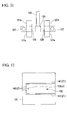
- FIG. 28 shows an example of the structure of a mode converter (converter) according to the related art.
- a waveguide 502 in a mode converter 510, includes an opening portion 525 which is provided in a forward end surface (the right side of FIG. 28 ) and from which radio waves are radiated.
- the waveguide 502 includes a plurality of post (column) walls 520 and upper and lower grounding conductor layers (cooper films) 521 and 522.
- a pin (plane circuit/waveguide converter) 523 is inserted as a feed portion into the waveguide 502.
- a millimeter-wave signal which is introduced from a transmission line 524 to the pin 523 is radiated as electromagnetic waves from the opening portion 525 provided on the front side of the waveguide 502.
- the mode converter 510 is formed by laminating a plurality of substrates 528A, 528B, and 528C.
- the pin 523 is formed by laminating the substrates 528B and 528C in which vias are formed in advance and by filling the vias with a conductive material.
- the length of the pin 523 is adjusted to a predetermined value to adjust impedance.
- a method for optimizing the distance between the pin 523 and the grounding conductor layer 522 is considered as one of impedance matching means.
- the vias are formed in advance in a plurality of substrates whose thickness has been determined and the plurality of substrates are laminated to manufacture the pin. Therefore, the length of the pin depends on the thickness of the substrates and is set to only a discrete value. As a result, it is difficult to set the length of the pin to a desired value. In addition, it is difficult to set the thickness of each of the substrates to be laminated and the thickness of each substrate depends on the availability of a material. Therefore, it is difficult to obtain a pin with an optimal length.
- the means When reflection loss is reduced by means other than the adjustment of the length of the pin, the means are likely to be a band limiting factor which causes a reduction in an available band. Therefore, the means are not the best method.
- the hollowing undesirable situations occur: transmission loss caused by an adhesive which is used to attach the substrates; a variation in transmission characteristics caused by the material forming each layer; and the positional deviation between the substrates when the substrates are laminated.
- the invention has been made in view of the above-mentioned problems and an object of the invention is to provide a method for manufacturing a mode converter which achieves signal transmission with low reflection loss and facilitates impedance matching.
- a first aspect of the present invention provides a method for manufacturing a mode converter including a substrate that is a single member and includes a first main surface, a second main surface opposite to the first main surface, and a micro hole which is formed in the first main surface and has a predetermined depth, grounding conductor layers that are formed on the first main surface and the second main surface, a plane circuit that is formed on the first main surface and is configured to transmit a high-frequency signal, and a pin that is formed so as to cover an inner surface of the micro hole and is electrically connected to the plane circuit, the method including: irradiating the substrate with laser light and thereby forming a first modified portion to a predetermined depth from one main surface of the substrate; removing the first modified portion and thereby forming the micro hole; and filling the micro hole with a conductive material to form the pin.
- the invention it is possible to adjust the length of the modified portion which is formed in the single substrate by laser modification and thus to adjust the length of the pin. Therefore, it is possible to achieve a pin with a predetermined length, without the length of the pin being a discrete value, unlike the related art. As a result, it is not necessary to adjust the length of the pin using, for example, other circuit elements and it is possible to achieve a mode converter with low reflection loss.
- the substrate is not a laminate of a plurality of substrates, but can be a substrate including a single base. Therefore, it is possible to avoid many undesirable situations, such as loss which is caused by an adhesive when a plurality of bases are laminated, a variation in characteristics caused by a material forming each layer, and positional deviation which occurs when layers are laminated.
- the grounding conductor layer may be formed at the same time as the pin is formed.
- the pin and the grounding conductor layer can be formed by the same process. Therefore, it is possible to reduce the number of processes and to improve manufacturing efficiency.
- the mode converter may further includes an electromagnetic wave shielding portion that passes through the substrate from the first main surface to the second main surface and is arranged so as to surround the micro hole in a plan view, when the first modified portion is formed, the substrate may be irradiated with the laser light and a second modified portion is formed so as to extend from the first main surface to the second main surface and to surround the micro hole in a plan view, the second modified portion may be removed at the same time as the first modified portion is removed, and a portion from which the second modified portion is removed may be filled with a conductive material to form the electromagnetic wave shielding portion at the same time as the micro hole is filled with the conductive material.
- the pin and the electromagnetic wave shielding portion can be formed by the same process. Therefore, it is possible to reduce the number of processes and to improve manufacturing efficiency.
- a second aspect of the present invention provides a mode converter including: a substrate that is a single member and includes a first main surface, a second main surface opposite to the first main surface, and a micro hole which is formed in the first main surface and has a predetermined depth; grounding conductor layers that are formed on the first main surface and the second main surface; a plane circuit that is formed on the first main surface and is configured to transmit a high-frequency signal; and a pin that is formed so as to cover an inner surface of the micro hole and is electrically connected to the plane circuit.
- the grounding conductor layer and the pin may be made of the same conductive material.
- an electromagnetic wave shielding portion that passes through the substrate from the first main surface to the second main surface and may be arranged so as to surround the micro hole in a plan view.
- the electromagnetic wave shielding portion may include a plurality of conductor posts that may be arranged so as to be separated from each other.
- the electromagnetic wave shielding portion may include a conductor post and a conductor wall that is continuous in at least one direction in a plan view.
- the method for manufacturing the mode converter of the above aspects it is possible to freely adjust the length of the pin and to achieve a mode converter which can reduce refection loss, without adjusting the length of the pin using, for example, other circuit elements.
- FIG. 1 is a perspective view schematically showing the structure of the mode converter 100.
- FIG. 2 is a cross-sectional view showing an example of the structure of the mode converter 100.
- FIG. 3 is an enlarged perspective view schematically showing a structure extending from a plane circuit to a pin.
- FIG. 4 is a cross-sectional view schematically showing a GND connection via.
- FIG. 5 is a plan view schematically showing conductor posts 114 which form a reflecting portion.
- reference numeral 100 denotes a mode converter.
- the mode converter 100 includes a glass substrate (substrate) 101 which is a single member (an integrated structure), an excitation pin structure 120 having a plane circuit (transmission path) 122 that can transmit a high-frequency signal and a pin (which is also referred to as a conductor pin) 123, first and second grounding conductor layers 111 and 112 which are connected to the ground potential of the reflecting portion, the conductor posts 114, and a waveguide 110.
- a glass substrate (substrate) 101 which is a single member (an integrated structure
- an excitation pin structure 120 having a plane circuit (transmission path) 122 that can transmit a high-frequency signal and a pin (which is also referred to as a conductor pin) 123
- first and second grounding conductor layers 111 and 112 which are connected to the ground potential of the reflecting portion
- the conductor posts 114 and a waveguide 110.
- the glass substrate which is a single member is not a laminated substrate of a plurality of substrates or a composite substrate, but is a glass substrate made of a single material.
- a quartz substrate or a semiconductor substrate that transmits electromagnetic waves may be used, instead of the glass substrate.
- the first grounding conductor layer 111 is provided on a front surface of the glass substrate 101.
- the second grounding conductor layer 112 is provided on a rear surface of the glass substrate 101.
- a plurality of conductor posts 114 are a plurality of post walls which are vertically provided between the first and second grounding conductor layers 111 and 112 and are arranged in a U-shape in the plan view of the glass substrate 101.
- the waveguide 110 is provided inside the plurality of conductor posts 114 (electromagnetic wave shielding portion) which are arranged in a U-shape in a plan view between the first grounding conductor layer 111 and the second grounding conductor layer 112.
- the waveguide 110 functions as a path through which an electromagnetic wave signal radiated from the pin 123 is propagated.
- the first and second grounding conductor layers 111 and 112 and the conductor posts 114 are not provided at one end of the waveguide 110 and the one end of the waveguide 110 is an opening portion (electromagnetic waves radiation portion) 102 from which the electromagnetic wave signal is radiated.
- the first and second grounding conductor layers 111 and 112 are, for example, cooper thin films which are provided on the front and rear surfaces of the glass substrate 101 and are provided on the entire front and rear surfaces of the glass substrate 101 except for at least a peripheral region of the pin 123.
- the plurality of conductor posts 114 are made of the same material as the grounding conductor layers 111 and 112 and pass through the glass substrate 101.
- the ends of the conductor posts 114 are connected to the grounding conductor layer 111 and the grounding conductor layer 112.
- the plurality of conductor posts 114 are arranged in a substantially rectangular U-shape which is parallel to three sides except for one side corresponding to the opening portion 102 among four sides of the glass substrate 101 in a plan view.
- the arrangement of the plurality of conductor posts 114 is set such that a high-frequency signal radiated from the pin 123 does not leak to the outside.
- a distance L between the central axes of the conductor posts 114 is set so as to be less than two times the diameter d of the conductor post 114, as shown in FIG. 5 . That is, a gap X between the closest conductor posts 114 is set so as to be less than the diameter d of the conductor post 114.
- the excitation pin structure 120 of the mode converter 100 includes the pin 123 which is formed so as to extend from an opening 111a provided in the first grounding conductor layer 111 to the inside of the glass substrate 101 and the plane circuit (transmission path) 122 which is connected to the outer surface of the pin 123 and is located above the first grounding conductor layer 111.
- An insulating portion 124 with a substantially constant thickness is provided on the first grounding conductor layer 111 and the transmission path 122 is formed on the outer surface of the insulating portion 124.
- the transmission path 122 is provided so as to overlap at least an opening region (111a) of the first grounding conductor layer 111 in the thickness direction of the substrate.
- the transmission path 122 has one end that is connected to an upper base end of the pin 123 and the other end that is connected to a GSG pad 125 on the insulating portion 124 and becomes a microstrip line. As shown in FIG.
- two GND pads 126 are provided on both sides of the GSG pad 125 so as to be separated from each other and to be arranged in two regions partitioned by the transmission path 122 on the insulating portion 124.
- a GND via 127 is adjacent to a side of each GND pad 126 that is opposite to the GSG pad 125.
- the GND via 127 is provided so as to extend from the surface of the transmission path 122 on the insulating portion 124 to the surface of the first grounding conductor layer 111 below the insulating portion 124.
- an "upper direction" means a direction from the rear surface to the front surface of the substrate in the thickness direction.
- the pin 123 includes a cylindrical body having one end that is a closed leading end 123a on a disk and has a substantially constant outside diameter H1.
- the pin 123 is formed in the glass substrate 101 so as to be vertical with respect to the front and rear surfaces of the glass substrate 101.
- a length H4 is set such that the leading end 123a arranged in the substrate does not come into contact with the second grounding conductor layer 112, which will be described below.
- a base end 123b which is the other end of the cylindrical body of the pin 123 is formed in the front surface of the glass substrate 101 which is the same surface of the first grounding conductor layer 111.
- the pin 123 includes a flange-shaped land 123c which is provided on the front surface of the glass substrate 101 so as to extend from the other end of the cylindrical body to the outside in a radial direction and is made of the same material as the first grounding conductor layer 111.
- the land 123c has a circular ring shape in a plan view in which a surface outer edge portion 123d is provided in the outer circumference and a circular ring portion 123e is provided in the inner circumference.
- the surface outer edge portion 123d is covered with the insulating portion 124.
- the upper surface of the circular ring portion 123e is covered with a conductor 122a which extends from the transmission path 122 and has a diameter that increases toward the thickness direction of the insulating portion 124.
- the circular ring portion 123e is electrically connected to the transmission path 122 through the conductor 122a.
- the inner surface (inside) of then pin 123 is covered with a conductor 122b connected to the conductor 122a.
- the outside diameter H3 of the surface outer edge portion 123d (the outside diameter of the land 123c), the outside diameter H2 of the conductor 122a which comes into contact with the land 123c, and the outside diameter H1 of the cylindrical body of the pin 123 are set such that H3 > H2 > H1 is satisfied.
- At least the inner surface of the pin 123 is made of a conductor, such as Cu, Ag, or Au.
- a central portion of the pin 123 may have a hollow structure or a structure in which it is filled with, for example, the same conductor as that forming the front surface or an insulating resin.
- the conductor can be formed by, for example, a plating method and a conductive paste filling method.
- FIGS. 6A to 6C show the shapes of the leading end of the pin 123 according to other embodiments.
- the pin 123 may have an end-rounded shape in which the leading end 123a is rounded.
- the pin 123 may have a shape in which the leading end is acute.
- the accuracy required to control the distance between the leading end of the pin and the second grounding conductor layer 112 is reduced, which is preferable. As a result, it is easy to perform impedance matching during manufacturing.
- the transmission path 122, the pin 123, the first grounding conductor layer 111, the second grounding conductor layer 112, and the conductor post 114 are formed by sequentially laminating a film made of titanium (Ti) or chrome (Cr) and a film made of copper (Cu) from the front surface side of the glass substrate 101 or the insulating portion 124. It is preferable to minimize the thickness of the film made of Ti or Cr to the extent that the accuracy of adhesion to the substrate is not damaged. For example, when the thickness of the film made of Cu is equal to or greater than 300 nm, it is preferable that the thickness of the film made of Ti or Cr is approximately 40 nm. In this case, both the transmission path 122 and the pin 123 are suitable for transmitting electromagnetic waves in a millimeter-wave band. For example, a copper portion can be a plated layer which will be described below.
- FIGS. 7A to 7P A method for manufacturing the mode converter 100 shown in FIGS. 1 to 5 will be described with reference to FIGS. 7A to 7P .
- FIGS. 7A to 7P are front sectional views sequentially showing processes of manufacturing a main portion of the glass substrate in stages during the manufacture of the waveguide.
- the glass substrate 101 serving as a base is prepared.
- the glass substrate 101 is a large-area glass substrate having a wafer shape and has a thickness of 850 ⁇ m.
- the glass substrate 101 is irradiated with laser light and a modified portion (first modified portion) ⁇ and a modified portion (second modified portion) ⁇ are formed.
- the modified portion ⁇ is formed to a desired depth corresponding to the length H4 of the pin 123.
- a plurality of modified portions ⁇ 3 corresponding to the plurality of conductor posts 114 are formed so as to pass through the glass substrate 101.
- the modified portions ⁇ are formed such that they have a diameter d and the distance X between two adjacent modified portions ⁇ is less than the diameter d.
- a substrate which is made of Pyrex (registered trademark) can be used as the glass substrate 101.
- Femtosecond laser light having a pulse width of 250 fs is used as the laser light. The laser light is focused and radiated to scan the glass substrate, thereby forming the modified portions.
- the dimensions (length and thickness) of the modified portions ⁇ and ⁇ can be controlled according to laser irradiation conditions (the size of the focal point and the scanning distance).
- the modified portion ⁇ and the modified portion ⁇ are removed by etching.
- etching is performed by immersing the glass substrate 101 having the modified portions ⁇ and ⁇ formed therein in a predetermined chemical in a container (not shown). Then, the modified portion ⁇ is wet-etched by the chemical from a first main surface (front surface) 101a of the glass substrate 101 and the modified portion ⁇ is wet-etched by the chemical from two main surfaces of the glass substrate 101. As a result, the modified portion ⁇ and the modified portion ⁇ are removed in the glass substrate 101.
- a micro hole ⁇ and a micro hole ⁇ are formed in the portions corresponding to the removed modified portions ⁇ and ⁇ .
- an acid solution having hydrofluoric acid as a main component or an alkali solution having potassium hydroxide as a main component can be used as the chemical.
- etching is performed using a phenomenon in which a non-modified portion is more rapidly etched than a modified portion. The use of this phenomenon makes it possible to form the micro holes ⁇ and ⁇ based on the shape of the modified portions ⁇ and ⁇ .
- the diameter of the micro holes ⁇ and ⁇ can be appropriately set in the range of 10 ⁇ m to 300 ⁇ m depending on the purpose of the portion to be manufactured.
- the micro hole ⁇ formed by the above-mentioned method (the modification of the substrate by laser irradiation and the etching of the modified portion with the acid solution) has a shape in which the bottom thereof is rounded as shown in FIG. 6A . Therefore, the pin formed in the micro hole ⁇ has an end-rounded shape as shown in FIG. 6A .
- the micro hole ⁇ and the micro hole ⁇ formed in the second process are filled with a conductive material and the pin 123 and the conductor post 114 are formed.
- a seed layer 121a is formed on the front surface 101a of the glass substrate 101 and in the micro holes ⁇ and ⁇ .
- a seed layer 121b is formed on the second main surface (rear surface) 101b of the glass substrate 101.
- the seed layers 121 a and 121b have, for example, a layer structure of Cr/Cu or a layer structure of Ti/Cu.
- the thickness of the seed layers 121 a and 121b is in the range of 10 nm to 500 nm.
- the seed layers 121a and 121b can be formed by a sputtering method.
- a plating resist 115 is formed around the micro hole ⁇ on the seed layer 121 a.
- the resist 115 has a circular ring shape in a plan view on the front surface 101 a of the glass substrate and is formed so as to cover a region corresponding to the opening 111a which is arranged in the outer circumference of then micro hole ⁇ and the land 123c.
- the inside diameter H3 of the resist 115 is set considering the outside diameter H3 of the land 123c.
- a liquid negative resist, a film-shaped negative resist, a liquid positive resist, or a film-shaped positive resist can be used as the resist 115.
- a copper layer is formed on the surfaces of the seed layers 121a and 121b except for the resist 115 by a plating method to form a layer which will be the pin 123, the first and second grounding conductor layers 111 and 112, and the conductor post 114.
- the pin 123 is formed in the micro hole ⁇ and on a portion of the front surface 101a of the glass substrate which will be the land 123c around the micro hole ⁇ .
- the first grounding conductor layer 111 is formed on the outside of the opening 111a of the glass substrate front surface 101a.
- the conductor post 114 is formed in the micro hole ⁇ .
- the second grounding conductor layer 112 is formed on the seed layer 121b formed on the rear surface 101b of the glass substrate 101.
- the thickness of the copper-plated layer is greater than at least a surface depth at which current density increases when a high-frequency signal in a millimeter-wave band flows.
- the surface depth is 270 nm. Therefore, a thickness of approximately 2 ⁇ m is enough.
- micro holes ⁇ and ⁇ may or may not be completely filled with the pin 123 and the conductor post 114 by copper plating.
- the resist 115 is removed as shown in FIG. 7H .
- the remaining seed layer 121a is etched. In this way, the first grounding conductor layer 111, the land 123c, and the opening portion 111a are formed.
- the insulating portion 124 is formed on the first grounding conductor layer 111 and the surface outer edge portion 123d which is an outer circumferential portion of the land 123c.
- An opening portion 124a is formed in a part of the insulating portion that corresponds to the micro hole ⁇ which will be the pin 123 and the circular ring portion 123e which is an inner circumferential portion of the land 123c provided around the micro hole ⁇ .
- An opening portion 124b is formed in a portion which will be the GND via 127 that is a termination portion of the plane circuit (transmission line) 122. That is, the insulating portion 124 is not formed in the opening portions 124a and 124b.
- the diameter of the opening portion 124a in the vicinity of the micro hole ⁇ is set to H2. Therefore, as shown in FIG. 2 , the outside diameter of the conductor 122a connected to the land 123c is set to H2.
- a liquid photosensitive resin is applied onto the first grounding conductor layer 111 and a portion of the front surface 111a of the glass substrate corresponding to the opening portion 111a by a spin coating method. Then, the opening portion 124a in the vicinity of the micro hole ⁇ and the opening portion 124b which will be the GND via 127 are removed by a photolithography method. In this way, the insulating portion 124 is formed. Then, the remaining photosensitive resin is hardened by a heat treatment.
- RIE reactive ion etching
- a seed layer 128 is formed on the surface of the insulating portion 124, on the circular ring portion 123e of the land 123c, in the micro hole ⁇ , and in the opening portion 124b.
- the seed layer 128 has the same layer structure as the seed layers 121a and 121b.
- the seed layer 128 has a layer structure of Cr/Cu or Ti/Cu.
- the thickness of the seed layer 128 is in the range of 10 nm to 500 nm.
- the seed layer 128 can be formed by a sputtering method.
- a resist 129 is formed on the surface of the seed layer 128 except for a portion which will be the transmission path 122 by plating.
- the resist 129 is formed so as to cover a region other than the portion which will be the transmission path 122 and portions which will be the GSG pad 125, the GND pad 126, and the GND via 127.
- the material forming the resist 129 may be the same as that forming the resist 115.
- the thickness of the copper-plated layer is greater than at least a surface depth at which current density increases when a high-frequency signal in a millimeter-wave band flows.
- the surface depth is 270 nm. Therefore, a thickness of about 2 ⁇ m is enough.
- the resist 129 is removed and the seed layer 128 is etched. In this way, the transmission path 122 which will be a microstrip line is formed.
- the mode converter 100 having the pin 123 can be formed on the glass substrate 101 by the above-mentioned processes.
- the glass substrate 101 which is a single member is used and the length of the modified portion ⁇ which will be the pin 123 can be set by modification using laser irradiation. Therefore, the pin 123 with any length can be formed as long as the length is within the thickness of the glass substrate 101. As a result, the length of the pin is not discrete, unlike the related art, and it is possible to obtain the optimal pin length at which the reflection of a signal is minimized. That is, it is possible to manufacture a mode converter which can effectively transmit a millimeter-wave signal transmitted from a wireless communication IC using the transmission path 122, without any loss.
- the state of impedance matching also depends on the diameter of the pin 123.
- the diameter of the micro hole ⁇ which will be the pin 123 can be adjusted by etching conditions. Therefore, it is possible to adjust the diameter of the pin 123 with higher accuracy than the related art in which the diameter of the micro hole is defined only by drilling or laser machining.
- the pin 123 can be formed in the single glass substrate 101, unlike the related art in which a plurality of substrates are laminated and vias are connected to each other by the land structure of the interface between the laminated layers. Therefore, a land structure does not need to be provided in the middle of the pin and it is possible to reduce the adverse effect of signal reflection due to the land structure in which the diameter of the pin is not constant.
- the mode converter 100 does not include a laminate of a plurality of substrates shown in FIG. 28 , but includes a single base. Therefore, it is possible to avoid all undesirable situations which occur when a plurality of bases are laminated, such as loss caused by an adhesive, a variation in the characteristics of each layer, and the positional deviation between layers.
- the manufacturing method of this embodiment it is possible to form the pin 123 and the plurality of conductor posts 114 which will be the reflecting portion 110 in parallel at the same time. Therefore, the number of processes required for manufacturing and the number of man-hours are reduced. As a result, it is possible to reduce the work time and manufacturing cost.
- the outside diameter H3 of the outer edge portion 123d (the outside diameter of the land 123c), the outside diameter H2 of the conductor 122a connected to the land 123c, and the outside diameter H1 of the pin 123 are set such that H3 > H2 > H1 is satisfied. Therefore, it is possible to prevent the conductor 122a from protruding from the outer edge portion 123d.
- the glass substrate 101 since the glass substrate 101 is used, it is possible to achieve a mode converter which has lighter weight and smaller loss than the related art using a substrate (FR4) in which an epoxy resin includes glass cloth (fiber).
- the diameter of the pin 123 is set so as to be constant from the base end 123b to the leading end 123a.
- the invention is not limited thereto.
- an angle formed between a straight line which is parallel to the front surface 101 a of the substrate and passes through the leading end 123a and a straight line indicating the side surface of the pin 123 may be ⁇ 0. That is, the pin 123 may be formed such that the diameter of the pin 123 at the leading end 123a is less than the diameter of the pin 123 at the base end 123b. In this case, a metal attachment effect in the micro hole ⁇ is improved and it is possible to reliably form the seed layer 121a using a sputtering method and to reliably form the first grounding conductor layer 111 using a plating method.
- an angle formed between a straight line indicating the front surface 101a of the substrate and a straight line indicating the side surface of the pin 123 may be ⁇ 1. That is, the pin 123 may be formed such that the diameter thereof at the leading end 123a is greater than the diameter thereof at the base end 123b. In this case, it is possible to smoothly introduce the millimeter-wave signal to the pin 123. In addition, it is possible to improve the efficiency of coupling to the waveguide. Therefore, it is possible to smoothly introduce the millimeter-wave signal to the pin 123.
- an angle formed between a straight line indicating the front surface 101a of the substrate and a straight line indicating the side surface of the pin 123 may be ⁇ 3 and an angle formed between a straight line indicating the rear surface 101b of the substrate and a straight line indicating the side surface of the pin 123 may be ⁇ 4. That is, the diameter of the pin 123 may decrease and then increase from the base end to the leading end 123a such that the pin 123 is narrow in the middle.
- the micro hole ⁇ needs to pass through the rear surface 101b of the glass substrate 101 and an opening 112a needs to be formed in the conductor layer 112 such that the second grounding conductor layer 112 on the rear surface is separated from the pin 123.
- This structure can respond to a case in which the length H4 of the pin 123 is desired to be large.
- the micro hole ⁇ is also formed in the rear surface 101b of the glass substrate 101, it is possible to reduce the etching time.
- the formation of the angle ⁇ 3 and the angle ⁇ 4 makes it possible to improve the metal attachment effect in the micro hole ⁇ and to reliably form the seed layer 121a and the first grounding conductor layer 111 using copper plating.
- the end of the micro hole ⁇ which is close to the rear surface 101b may be closed with an insulating material 123g.
- the end of the micro hole ⁇ which is close to the front surface 101 a may be closed with the insulating material 123g, which is not shown in the drawings.
- the leading end 123a of the pin 123 may be formed so as to have curvature.
- the leading end 123a shown in FIG. 6A does not have the corners shown in, for example, FIGS. 2 , 8, and 9 . Therefore, the electric field which is generated between the pin 123 and the second grounding conductor layer 112 is not concentrated on the corner and it is possible to uniformize the electric field between the pin 123 and the second grounding conductor layer 112.
- the end of the transmission line 122 extending from the pin 123 is the GSG pad 125 and the GND via 127 is adjacent to the GND pad 126.
- the installation position of the GND via is not limited to a side 127 of the GND pad 126 which is opposite to the GSG pad 125.
- the GND via may be provided on a side 127a of the GND pad 126 which is far away from the pin 123.
- the GND via may be provided on a side 127b of the GND pad 126 which is close to the pin 123.
- FIG. 11 is a plan view simultaneously showing the GND vias which are provided at different positions relative to the GND pad 126 in order to describe the position of the GND via.
- the GND via 127 may be provided at a position that is shifted by an arbitrary length in a direction from the GND pad 126 to the GND via 127a or may be provided at a position that is shifted by an arbitrary length in a direction from the GND pad 126 to the GND via 127b.
- the reflecting portion 110 includes the plurality of conductor posts 114.
- the invention is not limited thereto.
- a side that will be a rear wall opposite to the opening portion 102 from which radio waves are radiated from the mode converter may be formed by a plurality of conductor posts 114, similar to FIG. 1 , and two sides which extend in the direction from the pin 123 to the opening portion 102 may be conductor walls (electromagnetic wave shielding portions) 141 ( ⁇ 1) that are continuous in the direction, as shown in FIG. 12 .
- a continuous micro hole may be formed.
- the side which will be the rear wall is formed by a plurality of conductor posts 140. Therefore, even when a defect, such as the electrical opening of some conductor posts, occurs, the performance of the mode converter can be maintained by the remaining conductor posts connected to the grounding conductor layers.
- the conductor wall 141 serves as a side wall reflecting portion. This structure can more effectively prevent the leakage of electromagnetic waves than that in which a plurality of conductor posts are provided.
- the glass substrate 101 extends to the outside of the opening portion 102 in a plan view.
- the conductor wall 141 may be formed so as to extend to the end of the glass substrate 101 such that the glass substrate 101 does not extend to the outside of the opening portion 102.
- the reflecting portion 110 formed by a plurality of conductor posts 140 is formed on a side of the pin 123 opposite to the side on which the opening is formed. Therefore, in the first process and the second process, even when a long hole ⁇ 1 is formed in the glass substrate 101, the glass substrate 101 is not separated.
- two sides which extend in the direction from the pin 123 to the opening portion 102 may be long holes ⁇ 1 obtained by continuously forming a plurality of cylinders so as to overlap each other in a plan view, as shown in FIG. 13 .
- the three sides formed by the plurality of conductor posts 114 can be formed by a conductor wall 142 which is a U-shaped continuous long hole ⁇ 2 and the conductor posts 140 which are separated only in the vicinity of the opening portion 102.
- the pin is not surrounded by the posts, but the surrounding environment of the pin is a closed space. Therefore, it is possible to prevent leakage of electromagnetic waves from the pin when the electromagnetic waves are introduced.
- a conductor post 140 is provided in a region between the conductor wall 143 and each conductor wall 141 so as to be discontinuous with the conductor wall 143 and each conductor wall 141. In this case, since the only discontinuous portion is the post, it is possible to minimize the disturbance of the mode of electromagnetic waves in the discontinuous portion and to achieve a structure which is more mechanically stable than the structure shown in FIG. 14 .
- the glass substrate is continuous inside the reflecting portion 110 (mode converter 100) and outside the reflecting portion 110. Therefore, the glass substrate 101 is not separated.
- another conductor wall 144 (long hole ⁇ 4) which increases the width of the reflecting portion may be provided on the outside of the opening portion 102.
- a method for combining the conductor post 114 and the conductor wall 144 for the electromagnetic wave shielding portion, a method for arranging the conductor post 114 and the conductor wall 144, and the arrangement shape of the conductor post 114 and the conductor wall 144 are not limited to the structures shown in FIG. 1 and FIGS. 12 to 16 .
- the electromagnetic wave shielding portion may form an electromagnetic wave radiation portion which surrounds the pin 123 in plan view and can radiate electromagnetic waves from the pin 123 in one direction. It is preferable to design the electromagnetic wave shielding portion such that the glass substrate 101 is not separated when the micro hole ⁇ is formed.
- the diameter of the conductor post 114 is set so as to be constant from the front surface 101 a to the rear surface 101b of the glass substrate 101.
- the invention is not limited thereto.
- the diameter of the pin 123 may be reduced from the front surface 101a to the rear surface 101b such that an angle formed between a straight line indicating the rear surface 101b of the substrate and a straight line indicating the side surface of the pin 123 is ⁇ 5.
- the formation of the angle ⁇ 5 makes it possible to improve the metal attachment effect in the micro hole ⁇ and to reliably form the seed layer 121a and the first grounding conductor layer 111 using copper plating.
- the diameter of the pin 123 may be reduced and then increased from the front surface 101a to the rear surface 101b such that an angle formed between a straight line indicating the front surface 101a of the substrate and a straight line indicating the side surface of the pin 123 is ⁇ 6 and an angle formed between a straight line indicating the rear surface 101 b of the substrate and a straight line indicating the side surface of the pin 123 is ⁇ 7.
- the formation of the angle ⁇ 6 and the angle ⁇ 7 makes it possible to improve the metal attachment effect in the micro hole ⁇ and to reliably form the seed layer 121a and the first grounding conductor layer 111 using copper plating.
- the micro hole ⁇ 3 and the long hole ⁇ 1 may not be filled with a conductor and may be hollow.
- first and second grounding conductor layers 111 and 112 may be provided only in corresponding portions between the opposite inner surfaces of a conductor wall 147. In this case, it is preferable that both ends of the conductor posts 146 are reliably connected to the first and second grounding conductor layers 111 and 112.
- the reflecting portion 110 since the reflecting portion 110 includes the conductor walls 141, 142, 143, 144, and 147, it is possible to significantly reduce the leakage of electromagnetic waves, as compared to the case in which the reflecting portion 110 is formed only by a plurality of conductor posts 114. Therefore, it is possible to improve the radiation efficiency of an antenna and to reduce the radiation loss of a waveguide. Since the conductor wall is used, the area in which a current flow is larger than that when only the conductor posts 114 are used. Therefore, it is possible to significantly reduce the disturbance and breakdown of the transmission mode due to the electrical disconnection between the post wall 114 and the first and second grounding conductor layers 111 and 112, which are likely to occur in all of the post walls 114, and the risk thereof.
- the mode converter 100 may form a millimeter-wave communication module 200, as shown in FIG. 20 .
- the millimeter-wave communication module 200 includes the mode converter 100 and a wireless communication IC (semiconductor chip) 210 having an element that has a wireless transmission and reception function, is provided as an example of the waveguide 100, and is connected to the upper surface of the wireless communication IC in a flip-chip manner.
- the first grounding conductor layer 111 which will be a GND layer, the transmission path 122 on the insulating portion 124, and a circuit (not shown) which is provided on the same layer as these components are provided on the front surface of the glass substrate 101 in which the mode converter 100 is formed.
- a terminal 211 of the wireless communication IC (semiconductor chip) 210 is connected to the end of the transmission line 122 through the GSG pad 125.
- the influence of parasitic inductance on a high-frequency signal in a millimeter-wave band is very large. Therefore, a short-distance connection using not wire bonding but a bump is preferable.
- the mode converter 100 uses the microstrip line.
- the mode converter 100 may use a coplanar strip line.
- a signal line 132 is formed on the same layer as the first grounding conductor layer 111 which will be an upper GND layer of a PWA.
- FIG. 22 is a graph showing the simulation results indicating the relationship between the length of a pin and reflection loss.
- numbers following H indicate the length of the pin (unit: ⁇ m).
- Three-dimensional electromagnetic field analysis software HFSS was used for the simulation.
- the thickness of the glass substrate was set to 850 ⁇ m.
- the reflection of the signal is the minimum.
- a reflection coefficient is equal to or less than -20 dB.
- FIG. 23 shows a simulation model in the laminated-structure-type mode converter according to the related art shown in FIG. 28 .
- openings of printed circuit board post-wall waveguides (PWW) 510 and 510A having the pins 523 provided therein are arranged so as to face each other.
- Signal input/output ports are a port 524a and a port 524b provided at the ends of a microstrip line 524.
- the transmission mode (quasi-TEM mode) of a microstrip is converted into a TE10 mode which is the transmission mode of a waveguide through the pin 523.
- the distance between the centers of the pins 523 was set to 10 mm.
- FIG. 24 is a graph showing the simulation results of the reflection coefficient of the printed circuit board post-wall waveguide using the simulation model according to the related art shown in FIG. 23 .
- the distance between the pin and the rear post wall was optimized at 60 GHz.
- the length of the pin was set to a specific value which could be achieved by the laminated structure of the substrate according to the related art.
- a frequency range in which S11 ⁇ -20 dB is satisfied is defined as a band.
- FIG. 25 shows the simulation results after an impedance matching element is provided on the outside of a waveguide and the length of a pin is adjusted, in order to solve the impedance mismatching problem which is caused by the impossibility of freely adjusting the length of the pin in the related art.
- FIG. 26 shows a simulation model of a glass post-wall waveguide (PWW) in which a pin is formed by the mode converter manufacturing method according to the invention.
- Signal input/output ports are the ends 125 of microstrip lines and the transmission mode (quasi-TEM mode) of a microstrip is converted into a TE10 mode which is the transmission mode of a waveguide through the pin 123.
- the distance between the centers of excitation vias was set to 10 mm.
- FIG. 27 is a graph showing the simulation results of the glass post-wall waveguide (PWW) shown in FIG. 26 in which the pin is formed by the mode converter manufacturing method according to the invention.
- the distance between the pin and the rear post wall was optimized at 60 GHz.
- the length of the pin was optimized at 60 GHz.
- a frequency range in which S11 ⁇ -20 dB is satisfied is defined as a band.
- the invention can be widely applied to a high-capacity communication device which uses a millimeter-wave band and has a high transmission speed of several gigabits per second.
Abstract
Description
- The present invention relates to a mode converter and a method for manufacturing the same, and more particularly, to a technique that is used for a mode converter for millimeter-wave band communication.
- Priority is claimed on
Japanese Patent Application No. 2013-029486, filed February 18, 2013 - In recent years, high-capacity communication which uses a millimeter-wave band and has a high transmission speed of several gigabits per second [Gbps] has been proposed and a portion thereof has been achieved. In particular, the importance of a wireless communication device which operates in a band of 60 [GHz] has increased. In Japan, it is possible to use a wide frequency band of 59 [GHz] to 66 [GHz], without a license. Therefore, the wireless communication device is expected to be spread to the household sector. Therefore, the most urgent task is to achieve an inexpensive and small millimeter-wave communication module.
- NPL 1 and PTL1 disclose a millimeter-wave module using a waveguide (post-wall waveguide antenna: PWA) which is formed by a printed circuit board as a technique for achieving a small and inexpensive millimeter-wave communication module.
- As shown in
FIGS. 1 to 7 of PTL 1, in the technique disclosed in PTL 1, the side wall (metal wall) of a waveguide according to the related art is replaced with a through hole group (post group) of the printed circuit board. As shown inFIGS. 1 to 7 of PTL 1, a wireless communication IC (CMOS-IC) is mounted on the PWA. A millimeter-wave signal which is output from an IC (which is referred to as a semiconductor chip 4 in the specification of PTL 1; which holds for the following description) by a method, such as wire bonding or bump connection, is transmitted through a transmission line (which is referred to as aline 24 such as a microstrip, a coplanar strip, or a strip) formed by a plane circuit once. Then, the millimeter-wave signal is finally transmitted to a waveguide structure portion (which is referred to as a waveguide 2) through a plane circuit/waveguide conversion structure (which is referred to as a central conductor 23). -
FIG. 28 shows an example of the structure of a mode converter (converter) according to the related art. As shown inFIG. 28 , in amode converter 510, awaveguide 502 includes anopening portion 525 which is provided in a forward end surface (the right side ofFIG. 28 ) and from which radio waves are radiated. Thewaveguide 502 includes a plurality of post (column)walls 520 and upper and lower grounding conductor layers (cooper films) 521 and 522. A pin (plane circuit/waveguide converter) 523 is inserted as a feed portion into thewaveguide 502. A millimeter-wave signal which is introduced from atransmission line 524 to thepin 523 is radiated as electromagnetic waves from theopening portion 525 provided on the front side of thewaveguide 502. Themode converter 510 is formed by laminating a plurality ofsubstrates pin 523 is formed by laminating thesubstrates - In the design of a general high-frequency circuit, when a circuit A and a circuit B are connected to each other, it is necessary to perform impedance matching. This means that a signal is transmitted without being reflected at a connection point between the circuit A and the circuit B. That is, a signal needs to be transmitted without being reflected at a connection point between a plane circuit/transmission line as the circuit A and the waveguide as the circuit B.
- In the structure shown in
FIG. 28 , in a predetermined frequency band, the length of thepin 523 is adjusted to a predetermined value to adjust impedance. As a result, signal transmission with low reflection loss is achieved. In addition, a method for optimizing the distance between thepin 523 and thegrounding conductor layer 522 is considered as one of impedance matching means. - However, in a method for manufacturing the converter according to the related art, the vias are formed in advance in a plurality of substrates whose thickness has been determined and the plurality of substrates are laminated to manufacture the pin. Therefore, the length of the pin depends on the thickness of the substrates and is set to only a discrete value. As a result, it is difficult to set the length of the pin to a desired value. In addition, it is difficult to set the thickness of each of the substrates to be laminated and the thickness of each substrate depends on the availability of a material. Therefore, it is difficult to obtain a pin with an optimal length.
- When reflection loss is reduced by means other than the adjustment of the length of the pin, the means are likely to be a band limiting factor which causes a reduction in an available band. Therefore, the means are not the best method.
- In addition, for example, the hollowing undesirable situations occur: transmission loss caused by an adhesive which is used to attach the substrates; a variation in transmission characteristics caused by the material forming each layer; and the positional deviation between the substrates when the substrates are laminated.
- [PTL 1]
Japanese Unexamined Patent Application, First Publication No. 2011-109438 - [NPL 1] R. Suga, et al., "Cost-Effective 60-GHz Antenna-Package with End-Fire Radiation from Open-Ended Post-Wall Waveguide for Wireless File-Transfer System," 2011 IEEE MTT-S International Microwave Symposium, pp. 348-351
- The invention has been made in view of the above-mentioned problems and an object of the invention is to provide a method for manufacturing a mode converter which achieves signal transmission with low reflection loss and facilitates impedance matching.
- A first aspect of the present invention provides a method for manufacturing a mode converter including a substrate that is a single member and includes a first main surface, a second main surface opposite to the first main surface, and a micro hole which is formed in the first main surface and has a predetermined depth, grounding conductor layers that are formed on the first main surface and the second main surface, a plane circuit that is formed on the first main surface and is configured to transmit a high-frequency signal, and a pin that is formed so as to cover an inner surface of the micro hole and is electrically connected to the plane circuit, the method including: irradiating the substrate with laser light and thereby forming a first modified portion to a predetermined depth from one main surface of the substrate; removing the first modified portion and thereby forming the micro hole; and filling the micro hole with a conductive material to form the pin.
- According to the invention, it is possible to adjust the length of the modified portion which is formed in the single substrate by laser modification and thus to adjust the length of the pin. Therefore, it is possible to achieve a pin with a predetermined length, without the length of the pin being a discrete value, unlike the related art. As a result, it is not necessary to adjust the length of the pin using, for example, other circuit elements and it is possible to achieve a mode converter with low reflection loss.
- In addition, the substrate is not a laminate of a plurality of substrates, but can be a substrate including a single base. Therefore, it is possible to avoid many undesirable situations, such as loss which is caused by an adhesive when a plurality of bases are laminated, a variation in characteristics caused by a material forming each layer, and positional deviation which occurs when layers are laminated.
- In the method for manufacturing a mode converter according to above aspect, the grounding conductor layer may be formed at the same time as the pin is formed.
- According to the above-mentioned aspect of the invention, the pin and the grounding conductor layer can be formed by the same process. Therefore, it is possible to reduce the number of processes and to improve manufacturing efficiency.
- In the method for manufacturing a mode converter according to above aspect, the mode converter may further includes an electromagnetic wave shielding portion that passes through the substrate from the first main surface to the second main surface and is arranged so as to surround the micro hole in a plan view, when the first modified portion is formed, the substrate may be irradiated with the laser light and a second modified portion is formed so as to extend from the first main surface to the second main surface and to surround the micro hole in a plan view, the second modified portion may be removed at the same time as the first modified portion is removed, and a portion from which the second modified portion is removed may be filled with a conductive material to form the electromagnetic wave shielding portion at the same time as the micro hole is filled with the conductive material.
- According to the above aspect of the invention, the pin and the electromagnetic wave shielding portion can be formed by the same process. Therefore, it is possible to reduce the number of processes and to improve manufacturing efficiency.
- A second aspect of the present invention provides a mode converter including: a substrate that is a single member and includes a first main surface, a second main surface opposite to the first main surface, and a micro hole which is formed in the first main surface and has a predetermined depth; grounding conductor layers that are formed on the first main surface and the second main surface; a plane circuit that is formed on the first main surface and is configured to transmit a high-frequency signal; and a pin that is formed so as to cover an inner surface of the micro hole and is electrically connected to the plane circuit.
- In the mode converter according to above aspect, the grounding conductor layer and the pin may be made of the same conductive material.
- In the mode converter according to above aspect, an electromagnetic wave shielding portion that passes through the substrate from the first main surface to the second main surface and may be arranged so as to surround the micro hole in a plan view.
- In the mode converter according to above aspect, the electromagnetic wave shielding portion may include a plurality of conductor posts that may be arranged so as to be separated from each other.
- In the mode converter according to above aspect, the electromagnetic wave shielding portion may include a conductor post and a conductor wall that is continuous in at least one direction in a plan view.
- According to the method for manufacturing the mode converter of the above aspects, it is possible to freely adjust the length of the pin and to achieve a mode converter which can reduce refection loss, without adjusting the length of the pin using, for example, other circuit elements.
-
-
FIG. 1 is a perspective view showing a waveguide in a method for manufacturing a mode converter according to an embodiment of the invention. -
FIG. 2 is a front sectional view showing the mode converter according to the embodiment of the invention. -
FIG. 3 is a perspective view showing the method for manufacturing the mode converter according to the embodiment of the invention. -
FIG. 4 is an enlarged cross-sectional view showing a GND via in the method for manufacturing the mode converter according to the embodiment of the invention. -
FIG. 5 is a plan view schematically showing a reflecting portion in the method for manufacturing the mode converter according to the embodiment of the invention. -
FIG. 6A is a cross-sectional view schematically showing an example of a pin in the method for manufacturing the mode converter according to the embodiment of the invention. -
FIG. 6B is a cross-sectional view schematically showing an example of the pin in the method for manufacturing the mode converter according to the embodiment of the invention. -
FIG. 6C is a cross-sectional view schematically showing an example of the pin in the method for manufacturing the mode converter according to the embodiment of the invention. -
FIG. 7A is a cross-sectional view showing a process in the method for manufacturing the mode converter according to the embodiment of the invention. -
FIG. 7B is a cross-sectional view showing a process in the method for manufacturing the mode converter according to the embodiment of the invention. -
FIG. 7C is a cross-sectional view showing a process in the method for manufacturing the mode converter according to the embodiment of the invention. -
FIG. 7D is a cross-sectional view showing a process in the method for manufacturing the mode converter according to the embodiment of the invention. -
FIG. 7E is a cross-sectional view showing a process in the method for manufacturing the mode converter according to the embodiment of the invention. -
FIG. 7F is a cross-sectional view showing a process in the method for manufacturing the mode converter according to the embodiment of the invention. -
FIG. 7G is a cross-sectional view showing a process in the method for manufacturing the mode converter according to the embodiment of the invention. -
FIG. 7H is a cross-sectional view showing a process in the method for manufacturing the mode converter according to the embodiment of the invention. -
FIG. 7I is a cross-sectional view showing a process in the method for manufacturing the mode converter according to the embodiment of the invention. -
FIG. 7J is a cross-sectional view showing a process in the method for manufacturing the mode converter according to the embodiment of the invention. -
FIG. 7K is a cross-sectional view showing a process in the method for manufacturing the mode converter according to the embodiment of the invention. -
FIG. 7L is a cross-sectional view showing a process in the method for manufacturing the mode converter according to the embodiment of the invention. -
FIG. 7M is a cross-sectional view showing a process in the method for manufacturing the mode converter according to the embodiment of the invention. -
FIG. 8 is a cross-sectional view schematically showing another example of the pin in the method for manufacturing the mode converter according to the embodiment of the invention. -
FIG. 9 is a cross-sectional view schematically showing another example of the pin in the method for manufacturing the mode converter according to the embodiment of the invention. -
FIG. 10 is a cross-sectional view schematically showing another example of the pin in the method for manufacturing the mode converter according to the embodiment of the invention. -
FIG. 11 is a plan view schematically showing another example of the GND via in the method for manufacturing the mode converter according to the embodiment of the invention. -
FIG. 12 is a plan view schematically showing another example of the reflecting portion in the method for manufacturing the mode converter according to the embodiment of the invention. -
FIG. 13 is a perspective view showing another example of the reflecting portion in the method for manufacturing the mode converter according to the embodiment of the invention. -
FIG. 14 is a plan view schematically showing another example of the reflecting portion in the method for manufacturing the mode converter according to the embodiment of the invention. -
FIG. 15 is a plan view schematically showing another example of the reflecting portion in the method for manufacturing the mode converter according to the embodiment of the invention. -
FIG. 16 is a plan view schematically showing another example of the reflecting portion in the method for manufacturing the mode converter according to the embodiment of the invention. -
FIG. 17 is a plan view schematically showing another example of the reflecting portion in the method for manufacturing the mode converter according to the embodiment of the invention. -
FIG. 18 is a plan view schematically showing another example of the reflecting portion in the method for manufacturing the mode converter according to the embodiment of the invention. -
FIG. 19 is a perspective view schematically showing another example of the reflecting portion in the method for manufacturing the mode converter according to the embodiment of the invention. -
FIG. 20 is a cross-sectional view schematically showing an example of a millimeter-wave communication module in the method for manufacturing the mode converter according to the embodiment of the invention. -
FIG. 21 is a perspective view showing another example of the pin in the method for manufacturing the mode converter according to the embodiment of the invention. -
FIG. 22 is a graph showing the dependence of a reflection coefficient on the length of the pin in the method for manufacturing the mode converter according to the embodiment of the invention. -
FIG. 23 is a perspective view showing a mode converter according to the related art which is simulated as an experimental example. -
FIG. 24 is a graph showing the simulation results of a frequency band in the mode converter according to the related art as the experimental example. -
FIG. 25 is a graph showing the simulation results of the frequency band which is adjusted in the mode converter according to the related art as the experimental example. -
FIG. 26 is a perspective view showing a mode converter which is simulated in an embodiment of the method for manufacturing the mode converter according to the invention. -
FIG. 27 is a graph showing the simulation results of a frequency band in an embodiment of the method for manufacturing the mode converter according to the invention. -
FIG. 28 is a front sectional view showing the mode converter according to the related art. - Hereinafter, preferred embodiments of the invention will be described with reference to the drawings. The following embodiments are illustrative examples for ease of understanding of the purpose of the invention and do not limit the invention unless otherwise specified. In some cases, in the following drawings, for convenience, a main portion is enlarged in order to facilitate the understanding of characteristics of the invention and the dimensions and scale of each component may be different from the actual dimensions and scale. In addition, for convenience, some portions are omitted in order to facilitate the understanding of characteristics of the invention.
- The structure of a
mode converter 100 according to a first embodiment of the invention will be described with reference toFIGS. 1 to 5 .FIG. 1 is a perspective view schematically showing the structure of themode converter 100.FIG. 2 is a cross-sectional view showing an example of the structure of themode converter 100.FIG. 3 is an enlarged perspective view schematically showing a structure extending from a plane circuit to a pin.FIG. 4 is a cross-sectional view schematically showing a GND connection via.FIG. 5 is a plan view schematically showingconductor posts 114 which form a reflecting portion. In the drawings,reference numeral 100 denotes a mode converter. - As shown in
FIGS. 1 and2 , themode converter 100 according to this embodiment includes a glass substrate (substrate) 101 which is a single member (an integrated structure), anexcitation pin structure 120 having a plane circuit (transmission path) 122 that can transmit a high-frequency signal and a pin (which is also referred to as a conductor pin) 123, first and second grounding conductor layers 111 and 112 which are connected to the ground potential of the reflecting portion, the conductor posts 114, and awaveguide 110. - The glass substrate which is a single member is not a laminated substrate of a plurality of substrates or a composite substrate, but is a glass substrate made of a single material. For example, a quartz substrate or a semiconductor substrate that transmits electromagnetic waves may be used, instead of the glass substrate.
- The first
grounding conductor layer 111 is provided on a front surface of theglass substrate 101. - The second
grounding conductor layer 112 is provided on a rear surface of theglass substrate 101. A plurality of conductor posts 114 (electromagnetic wave shielding portion) are a plurality of post walls which are vertically provided between the first and second grounding conductor layers 111 and 112 and are arranged in a U-shape in the plan view of theglass substrate 101. - The
waveguide 110 is provided inside the plurality of conductor posts 114 (electromagnetic wave shielding portion) which are arranged in a U-shape in a plan view between the firstgrounding conductor layer 111 and the secondgrounding conductor layer 112. Thewaveguide 110 functions as a path through which an electromagnetic wave signal radiated from thepin 123 is propagated. The first and second grounding conductor layers 111 and 112 and the conductor posts 114 are not provided at one end of thewaveguide 110 and the one end of thewaveguide 110 is an opening portion (electromagnetic waves radiation portion) 102 from which the electromagnetic wave signal is radiated. - Each component will be described in detail below.
- The first and second grounding conductor layers 111 and 112 are, for example, cooper thin films which are provided on the front and rear surfaces of the
glass substrate 101 and are provided on the entire front and rear surfaces of theglass substrate 101 except for at least a peripheral region of thepin 123. - As shown in
FIG. 1 , the plurality ofconductor posts 114 are made of the same material as the grounding conductor layers 111 and 112 and pass through theglass substrate 101. The ends of the conductor posts 114 are connected to thegrounding conductor layer 111 and thegrounding conductor layer 112. The plurality ofconductor posts 114 are arranged in a substantially rectangular U-shape which is parallel to three sides except for one side corresponding to theopening portion 102 among four sides of theglass substrate 101 in a plan view. The arrangement of the plurality of conductor posts 114 is set such that a high-frequency signal radiated from thepin 123 does not leak to the outside. - Specifically, when adjacent conductor posts 114 are arranged so as to be separated from each other, a distance L between the central axes of the conductor posts 114 is set so as to be less than two times the diameter d of the
conductor post 114, as shown inFIG. 5 . That is, a gap X between the closest conductor posts 114 is set so as to be less than the diameter d of theconductor post 114. - As shown in
FIGS. 1 to 3 , theexcitation pin structure 120 of themode converter 100 includes thepin 123 which is formed so as to extend from anopening 111a provided in the firstgrounding conductor layer 111 to the inside of theglass substrate 101 and the plane circuit (transmission path) 122 which is connected to the outer surface of thepin 123 and is located above the firstgrounding conductor layer 111. - An insulating
portion 124 with a substantially constant thickness is provided on the firstgrounding conductor layer 111 and thetransmission path 122 is formed on the outer surface of the insulatingportion 124. Thetransmission path 122 is provided so as to overlap at least an opening region (111a) of the firstgrounding conductor layer 111 in the thickness direction of the substrate. Thetransmission path 122 has one end that is connected to an upper base end of thepin 123 and the other end that is connected to aGSG pad 125 on the insulatingportion 124 and becomes a microstrip line. As shown inFIG. 3 , two GNDpads 126 are provided on both sides of theGSG pad 125 so as to be separated from each other and to be arranged in two regions partitioned by thetransmission path 122 on the insulatingportion 124. As shown inFIG. 3 , a GND via 127 is adjacent to a side of eachGND pad 126 that is opposite to theGSG pad 125. As shown inFIG. 4 , the GND via 127 is provided so as to extend from the surface of thetransmission path 122 on the insulatingportion 124 to the surface of the firstgrounding conductor layer 111 below the insulatingportion 124. In this embodiment, an "upper direction" means a direction from the rear surface to the front surface of the substrate in the thickness direction. - As shown in
FIG. 2 , thepin 123 includes a cylindrical body having one end that is a closedleading end 123a on a disk and has a substantially constant outside diameter H1. Thepin 123 is formed in theglass substrate 101 so as to be vertical with respect to the front and rear surfaces of theglass substrate 101. A length H4 is set such that theleading end 123a arranged in the substrate does not come into contact with the secondgrounding conductor layer 112, which will be described below. Abase end 123b which is the other end of the cylindrical body of thepin 123 is formed in the front surface of theglass substrate 101 which is the same surface of the firstgrounding conductor layer 111. In addition, thepin 123 includes a flange-shapedland 123c which is provided on the front surface of theglass substrate 101 so as to extend from the other end of the cylindrical body to the outside in a radial direction and is made of the same material as the firstgrounding conductor layer 111. Theland 123c has a circular ring shape in a plan view in which a surfaceouter edge portion 123d is provided in the outer circumference and acircular ring portion 123e is provided in the inner circumference. The surfaceouter edge portion 123d is covered with the insulatingportion 124. The upper surface of thecircular ring portion 123e is covered with aconductor 122a which extends from thetransmission path 122 and has a diameter that increases toward the thickness direction of the insulatingportion 124. Thecircular ring portion 123e is electrically connected to thetransmission path 122 through theconductor 122a. The inner surface (inside) of then pin 123 is covered with aconductor 122b connected to theconductor 122a. - The outside diameter H3 of the surface
outer edge portion 123d (the outside diameter of theland 123c), the outside diameter H2 of theconductor 122a which comes into contact with theland 123c, and the outside diameter H1 of the cylindrical body of thepin 123 are set such that H3 > H2 > H1 is satisfied. - At least the inner surface of the
pin 123 is made of a conductor, such as Cu, Ag, or Au. A central portion of thepin 123 may have a hollow structure or a structure in which it is filled with, for example, the same conductor as that forming the front surface or an insulating resin. The conductor can be formed by, for example, a plating method and a conductive paste filling method. -
FIGS. 6A to 6C show the shapes of the leading end of thepin 123 according to other embodiments. As shown inFIG. 6A , thepin 123 may have an end-rounded shape in which theleading end 123a is rounded. Alternatively, as shown inFIGS. 6B and6C , thepin 123 may have a shape in which the leading end is acute. When thepin 123 has the acute leading end as shown inFIGS. 6B and6C , the accuracy required to control the distance between the leading end of the pin and the secondgrounding conductor layer 112 is reduced, which is preferable. As a result, it is easy to perform impedance matching during manufacturing. - The
transmission path 122, thepin 123, the firstgrounding conductor layer 111, the secondgrounding conductor layer 112, and theconductor post 114 are formed by sequentially laminating a film made of titanium (Ti) or chrome (Cr) and a film made of copper (Cu) from the front surface side of theglass substrate 101 or the insulatingportion 124. It is preferable to minimize the thickness of the film made of Ti or Cr to the extent that the accuracy of adhesion to the substrate is not damaged. For example, when the thickness of the film made of Cu is equal to or greater than 300 nm, it is preferable that the thickness of the film made of Ti or Cr is approximately 40 nm. In this case, both thetransmission path 122 and thepin 123 are suitable for transmitting electromagnetic waves in a millimeter-wave band. For example, a copper portion can be a plated layer which will be described below. - A method for manufacturing the
mode converter 100 shown inFIGS. 1 to 5 will be described with reference toFIGS. 7A to 7P . -
FIGS. 7A to 7P are front sectional views sequentially showing processes of manufacturing a main portion of the glass substrate in stages during the manufacture of the waveguide. - First, as shown in
FIG. 7A , as a preparation process, theglass substrate 101 serving as a base is prepared. For example, theglass substrate 101 is a large-area glass substrate having a wafer shape and has a thickness of 850 µm. - Then, as shown in
FIG. 7B , as a first process, theglass substrate 101 is irradiated with laser light and a modified portion (first modified portion) α and a modified portion (second modified portion) β are formed. - The modified portion α is formed to a desired depth corresponding to the length H4 of the
pin 123. A plurality of modified portions β3 corresponding to the plurality ofconductor posts 114 are formed so as to pass through theglass substrate 101. The modified portions β are formed such that they have a diameter d and the distance X between two adjacent modified portions β is less than the diameter d. For example, a substrate which is made of Pyrex (registered trademark) can be used as theglass substrate 101. Femtosecond laser light having a pulse width of 250 fs is used as the laser light. The laser light is focused and radiated to scan the glass substrate, thereby forming the modified portions. The dimensions (length and thickness) of the modified portions α and β can be controlled according to laser irradiation conditions (the size of the focal point and the scanning distance). - Then, as a second process, the modified portion α and the modified portion β are removed by etching. In the etching process, etching is performed by immersing the
glass substrate 101 having the modified portions α and β formed therein in a predetermined chemical in a container (not shown). Then, the modified portion α is wet-etched by the chemical from a first main surface (front surface) 101a of theglass substrate 101 and the modified portion β is wet-etched by the chemical from two main surfaces of theglass substrate 101. As a result, the modified portion α and the modified portion β are removed in theglass substrate 101. - As shown in
FIG. 7C , a micro hole α and a micro hole β are formed in the portions corresponding to the removed modified portions α and β. In this embodiment, an acid solution having hydrofluoric acid as a main component or an alkali solution having potassium hydroxide as a main component can be used as the chemical. In the second process, etching is performed using a phenomenon in which a non-modified portion is more rapidly etched than a modified portion. The use of this phenomenon makes it possible to form the micro holes α and β based on the shape of the modified portions α and β. In this embodiment, the diameter of the micro holes α and β can be appropriately set in the range of 10 µm to 300 µm depending on the purpose of the portion to be manufactured. - The micro hole α formed by the above-mentioned method (the modification of the substrate by laser irradiation and the etching of the modified portion with the acid solution) has a shape in which the bottom thereof is rounded as shown in
FIG. 6A . Therefore, the pin formed in the micro hole α has an end-rounded shape as shown inFIG. 6A . - Then, as a third process, the micro hole α and the micro hole β formed in the second process are filled with a conductive material and the
pin 123 and theconductor post 114 are formed. - First, as shown in
FIG. 7D , aseed layer 121a is formed on thefront surface 101a of theglass substrate 101 and in the micro holes α and β. As shown inFIG. 7E , aseed layer 121b is formed on the second main surface (rear surface) 101b of theglass substrate 101. The seed layers 121 a and 121b have, for example, a layer structure of Cr/Cu or a layer structure of Ti/Cu. The thickness of the seed layers 121 a and 121b is in the range of 10 nm to 500 nm. The seed layers 121a and 121b can be formed by a sputtering method. - Then, as shown in
FIG. 7F , a plating resist 115 is formed around the micro hole α on theseed layer 121 a. The resist 115 has a circular ring shape in a plan view on thefront surface 101 a of the glass substrate and is formed so as to cover a region corresponding to theopening 111a which is arranged in the outer circumference of then micro hole α and theland 123c. The inside diameter H3 of the resist 115 is set considering the outside diameter H3 of theland 123c. For example, a liquid negative resist, a film-shaped negative resist, a liquid positive resist, or a film-shaped positive resist can be used as the resist 115. - Then, as shown in
FIG. 7G , a copper layer is formed on the surfaces of theseed layers pin 123, the first and second grounding conductor layers 111 and 112, and theconductor post 114. Thepin 123 is formed in the micro hole α and on a portion of thefront surface 101a of the glass substrate which will be theland 123c around the micro hole α. The firstgrounding conductor layer 111 is formed on the outside of theopening 111a of the glasssubstrate front surface 101a. Theconductor post 114 is formed in the micro hole β. - The second
grounding conductor layer 112 is formed on theseed layer 121b formed on therear surface 101b of theglass substrate 101. - It is preferable that the thickness of the copper-plated layer is greater than at least a surface depth at which current density increases when a high-frequency signal in a millimeter-wave band flows. When a high-frequency signal of 60 GHz is used, the surface depth is 270 nm. Therefore, a thickness of approximately 2 µm is enough.
- The micro holes α and β may or may not be completely filled with the
pin 123 and theconductor post 114 by copper plating. - Then, as a resist removal process, the resist 115 is removed as shown in
FIG. 7H . In addition, the remainingseed layer 121a is etched. In this way, the firstgrounding conductor layer 111, theland 123c, and theopening portion 111a are formed. - Then, as a fourth process, as shown in
FIG. 7I , the insulatingportion 124 is formed on the firstgrounding conductor layer 111 and the surfaceouter edge portion 123d which is an outer circumferential portion of theland 123c. Anopening portion 124a is formed in a part of the insulating portion that corresponds to the micro hole α which will be thepin 123 and thecircular ring portion 123e which is an inner circumferential portion of theland 123c provided around the micro hole α. Anopening portion 124b is formed in a portion which will be the GND via 127 that is a termination portion of the plane circuit (transmission line) 122. That is, the insulatingportion 124 is not formed in the openingportions - The diameter of the
opening portion 124a in the vicinity of the micro hole α is set to H2. Therefore, as shown inFIG. 2 , the outside diameter of theconductor 122a connected to theland 123c is set to H2. - As the fourth process, first, in order to form the insulating
portion 124, for example, a liquid photosensitive resin is applied onto the firstgrounding conductor layer 111 and a portion of thefront surface 111a of the glass substrate corresponding to theopening portion 111a by a spin coating method. Then, theopening portion 124a in the vicinity of the micro hole α and theopening portion 124b which will be the GND via 127 are removed by a photolithography method. In this way, the insulatingportion 124 is formed. Then, the remaining photosensitive resin is hardened by a heat treatment. - When the photosensitive resin remains on the
circular ring portion 123e in theopening portion 124a, a reactive ion etching (RIE) process using CF4 gas or O2 gas is preferably performed to remove the remaining photosensitive resin. - Then, the
transmission path 122 is formed. As shown inFIG. 7J , aseed layer 128 is formed on the surface of the insulatingportion 124, on thecircular ring portion 123e of theland 123c, in the micro hole α, and in theopening portion 124b. Theseed layer 128 has the same layer structure as theseed layers seed layer 128 has a layer structure of Cr/Cu or Ti/Cu. The thickness of theseed layer 128 is in the range of 10 nm to 500 nm. Theseed layer 128 can be formed by a sputtering method. - Then, as a resist forming process which is performed before a transmission path forming process, as shown in
FIG. 7K , a resist 129 is formed on the surface of theseed layer 128 except for a portion which will be thetransmission path 122 by plating. The resist 129 is formed so as to cover a region other than the portion which will be thetransmission path 122 and portions which will be theGSG pad 125, theGND pad 126, and the GND via 127. The material forming the resist 129 may be the same as that forming the resist 115. - Then, as the transmission path forming process, as shown in
FIG. 7N , copper plating is performed for the surface of theseed layer 128 except for the resist 129 to form a layer which will be thetransmission path 122. It is preferable that the thickness of the copper-plated layer is greater than at least a surface depth at which current density increases when a high-frequency signal in a millimeter-wave band flows. When a high-frequency signal of 60 GHz is used, the surface depth is 270 nm. Therefore, a thickness of about 2 µm is enough. - Then, as shown in
FIG. 7M , the resist 129 is removed and theseed layer 128 is etched. In this way, thetransmission path 122 which will be a microstrip line is formed. - The
mode converter 100 having thepin 123 can be formed on theglass substrate 101 by the above-mentioned processes. - In this embodiment, the
glass substrate 101 which is a single member is used and the length of the modified portion α which will be thepin 123 can be set by modification using laser irradiation. Therefore, thepin 123 with any length can be formed as long as the length is within the thickness of theglass substrate 101. As a result, the length of the pin is not discrete, unlike the related art, and it is possible to obtain the optimal pin length at which the reflection of a signal is minimized. That is, it is possible to manufacture a mode converter which can effectively transmit a millimeter-wave signal transmitted from a wireless communication IC using thetransmission path 122, without any loss. - It is considered that the state of impedance matching also depends on the diameter of the
pin 123. In this embodiment, the diameter of the micro hole α which will be thepin 123 can be adjusted by etching conditions. Therefore, it is possible to adjust the diameter of thepin 123 with higher accuracy than the related art in which the diameter of the micro hole is defined only by drilling or laser machining. - In the
mode converter 100 according to this embodiment, thepin 123 can be formed in thesingle glass substrate 101, unlike the related art in which a plurality of substrates are laminated and vias are connected to each other by the land structure of the interface between the laminated layers. Therefore, a land structure does not need to be provided in the middle of the pin and it is possible to reduce the adverse effect of signal reflection due to the land structure in which the diameter of the pin is not constant. - The
mode converter 100 according to this embodiment does not include a laminate of a plurality of substrates shown inFIG. 28 , but includes a single base. Therefore, it is possible to avoid all undesirable situations which occur when a plurality of bases are laminated, such as loss caused by an adhesive, a variation in the characteristics of each layer, and the positional deviation between layers. - According the manufacturing method of this embodiment, it is possible to form the
pin 123 and the plurality ofconductor posts 114 which will be the reflectingportion 110 in parallel at the same time. Therefore, the number of processes required for manufacturing and the number of man-hours are reduced. As a result, it is possible to reduce the work time and manufacturing cost. - In this embodiment, the outside diameter H3 of the
outer edge portion 123d (the outside diameter of theland 123c), the outside diameter H2 of theconductor 122a connected to theland 123c, and the outside diameter H1 of thepin 123 are set such that H3 > H2 > H1 is satisfied. Therefore, it is possible to prevent theconductor 122a from protruding from theouter edge portion 123d. - In post-processing (when a resist or a resin is formed), when the
outer edge portion 123d is misaligned, when the outside diameter H3 increases with respect to the outside diameters H2 and H1, the possibility that the cutting of a line due to the misalignment will be avoided increases. - According to this embodiment, since the
glass substrate 101 is used, it is possible to achieve a mode converter which has lighter weight and smaller loss than the related art using a substrate (FR4) in which an epoxy resin includes glass cloth (fiber). - In the above-described embodiment, as shown in
FIG. 2 , the diameter of thepin 123 is set so as to be constant from thebase end 123b to theleading end 123a. However, the invention is not limited thereto. As shown inFIG. 8 , in the cross section including a center line of thepin 123 in the thickness direction, an angle formed between a straight line which is parallel to thefront surface 101 a of the substrate and passes through theleading end 123a and a straight line indicating the side surface of thepin 123 may be θ0. That is, thepin 123 may be formed such that the diameter of thepin 123 at theleading end 123a is less than the diameter of thepin 123 at thebase end 123b. In this case, a metal attachment effect in the micro hole α is improved and it is possible to reliably form theseed layer 121a using a sputtering method and to reliably form the firstgrounding conductor layer 111 using a plating method. - As shown in
FIG. 9 , in the cross section including the center line of thepin 123 in the thickness direction, an angle formed between a straight line indicating thefront surface 101a of the substrate and a straight line indicating the side surface of thepin 123 may be θ1. That is, thepin 123 may be formed such that the diameter thereof at theleading end 123a is greater than the diameter thereof at thebase end 123b. In this case, it is possible to smoothly introduce the millimeter-wave signal to thepin 123. In addition, it is possible to improve the efficiency of coupling to the waveguide. Therefore, it is possible to smoothly introduce the millimeter-wave signal to thepin 123. - As shown in
FIG. 10 , in the cross section including the center line of thepin 123 in the thickness direction, an angle formed between a straight line indicating thefront surface 101a of the substrate and a straight line indicating the side surface of thepin 123 may be θ3 and an angle formed between a straight line indicating therear surface 101b of the substrate and a straight line indicating the side surface of thepin 123 may be θ4. That is, the diameter of thepin 123 may decrease and then increase from the base end to theleading end 123a such that thepin 123 is narrow in the middle. In this case, the micro hole α needs to pass through therear surface 101b of theglass substrate 101 and anopening 112a needs to be formed in theconductor layer 112 such that the secondgrounding conductor layer 112 on the rear surface is separated from thepin 123. This structure can respond to a case in which the length H4 of thepin 123 is desired to be large. In addition, since the micro hole α is also formed in therear surface 101b of theglass substrate 101, it is possible to reduce the etching time. - The formation of the angle θ3 and the angle θ4 makes it possible to improve the metal attachment effect in the micro hole α and to reliably form the
seed layer 121a and the firstgrounding conductor layer 111 using copper plating. - As shown in
FIG. 10 , the end of the micro hole α which is close to therear surface 101b may be closed with an insulatingmaterial 123g. In addition, the end of the micro hole α which is close to thefront surface 101 a may be closed with the insulatingmaterial 123g, which is not shown in the drawings. - As shown in
FIG. 6A , theleading end 123a of thepin 123 may be formed so as to have curvature. Theleading end 123a shown inFIG. 6A does not have the corners shown in, for example,FIGS. 2 ,8, and 9 . Therefore, the electric field which is generated between thepin 123 and the secondgrounding conductor layer 112 is not concentrated on the corner and it is possible to uniformize the electric field between thepin 123 and the secondgrounding conductor layer 112. - In this embodiment shown in
FIG. 3 , the end of thetransmission line 122 extending from thepin 123 is theGSG pad 125 and the GND via 127 is adjacent to theGND pad 126. However, the invention is not limited thereto. As shown inFIG. 11 , the installation position of the GND via is not limited to aside 127 of theGND pad 126 which is opposite to theGSG pad 125. The GND via may be provided on aside 127a of theGND pad 126 which is far away from thepin 123. In addition, the GND via may be provided on aside 127b of theGND pad 126 which is close to thepin 123.FIG. 11 is a plan view simultaneously showing the GND vias which are provided at different positions relative to theGND pad 126 in order to describe the position of the GND via. - The GND via 127 may be provided at a position that is shifted by an arbitrary length in a direction from the
GND pad 126 to the GND via 127a or may be provided at a position that is shifted by an arbitrary length in a direction from theGND pad 126 to the GND via 127b. - In this embodiment, as shown in
FIG. 1 , the reflectingportion 110 includes the plurality of conductor posts 114. However, the invention is not limited thereto. In the plan view ofFIG. 1 , among three sides formed by the reflectingportion 110, a side that will be a rear wall opposite to theopening portion 102 from which radio waves are radiated from the mode converter may be formed by a plurality of conductor posts 114, similar toFIG. 1 , and two sides which extend in the direction from thepin 123 to theopening portion 102 may be conductor walls (electromagnetic wave shielding portions) 141 (β1) that are continuous in the direction, as shown inFIG. 12 . In this case, in the first process and the second process, a continuous micro hole may be formed. - The side which will be the rear wall is formed by a plurality of conductor posts 140. Therefore, even when a defect, such as the electrical opening of some conductor posts, occurs, the performance of the mode converter can be maintained by the remaining conductor posts connected to the grounding conductor layers.
- In addition, the
conductor wall 141 serves as a side wall reflecting portion. This structure can more effectively prevent the leakage of electromagnetic waves than that in which a plurality of conductor posts are provided. - In this embodiment, as shown in
FIG. 1 , theglass substrate 101 extends to the outside of theopening portion 102 in a plan view. However, the invention is not limited thereto. As shown inFIG. 12 , theconductor wall 141 may be formed so as to extend to the end of theglass substrate 101 such that theglass substrate 101 does not extend to the outside of theopening portion 102. In this case, the reflectingportion 110 formed by a plurality of conductor posts 140 is formed on a side of thepin 123 opposite to the side on which the opening is formed. Therefore, in the first process and the second process, even when a long hole β1 is formed in theglass substrate 101, theglass substrate 101 is not separated. - In this structure, since the side wall in the traveling direction of electromagnetic waves is a continuous wall, it is possible to prevent the disturbance of the mode of electromagnetic waves due to the discontinuous arrangement of conductors.
- Among three sides formed by the reflecting
portion 110, two sides which extend in the direction from thepin 123 to theopening portion 102 may be long holes β1 obtained by continuously forming a plurality of cylinders so as to overlap each other in a plan view, as shown inFIG. 13 . - As shown in
FIG. 14 , the three sides formed by the plurality of conductor posts 114 (reflecting portion 110) can be formed by aconductor wall 142 which is a U-shaped continuous long hole β2 and the conductor posts 140 which are separated only in the vicinity of theopening portion 102. In this case, the pin is not surrounded by the posts, but the surrounding environment of the pin is a closed space. Therefore, it is possible to prevent leakage of electromagnetic waves from the pin when the electromagnetic waves are introduced. - As shown in
FIG. 15 , among three sides formed by the reflectingportion 110, two sides which extend in the direction from thepin 123 to theopening portion 102 are formed by long holes β1 (conductor walls 141) and a side which will be the rear wall opposite to theopening portion 102 is formed by a long hole β3 (conductor wall 143). Aconductor post 140 is provided in a region between theconductor wall 143 and eachconductor wall 141 so as to be discontinuous with theconductor wall 143 and eachconductor wall 141. In this case, since the only discontinuous portion is the post, it is possible to minimize the disturbance of the mode of electromagnetic waves in the discontinuous portion and to achieve a structure which is more mechanically stable than the structure shown inFIG. 14 . - As such, when the reflecting
portion 110 is discontinuous, the glass substrate is continuous inside the reflecting portion 110 (mode converter 100) and outside the reflectingportion 110. Therefore, theglass substrate 101 is not separated. - As shown in
FIG. 16 , another conductor wall 144 (long hole β4) which increases the width of the reflecting portion may be provided on the outside of theopening portion 102. In this case, it is possible to form an H-plane sectorial horn antenna and to improve an antenna gain. - In the invention, a method for combining the
conductor post 114 and theconductor wall 144 for the electromagnetic wave shielding portion, a method for arranging theconductor post 114 and theconductor wall 144, and the arrangement shape of theconductor post 114 and theconductor wall 144 are not limited to the structures shown inFIG. 1 andFIGS. 12 to 16 . The electromagnetic wave shielding portion may form an electromagnetic wave radiation portion which surrounds thepin 123 in plan view and can radiate electromagnetic waves from thepin 123 in one direction. It is preferable to design the electromagnetic wave shielding portion such that theglass substrate 101 is not separated when the micro hole β is formed. - In the above-described embodiment, as shown in
FIGS. 1 and2 , the diameter of theconductor post 114 is set so as to be constant from thefront surface 101 a to therear surface 101b of theglass substrate 101. However, the invention is not limited thereto. As shown inFIG. 17 , in the cross section including the center line of thepin 123 in the thickness direction, the diameter of thepin 123 may be reduced from thefront surface 101a to therear surface 101b such that an angle formed between a straight line indicating therear surface 101b of the substrate and a straight line indicating the side surface of thepin 123 is θ5. In this case, it is possible to improve the metal attachment effect in the micro hole β and to reliably form theseed layer 121a and theconductor post 114 using copper plating. In addition, the formation of the angle θ5 makes it possible to improve the metal attachment effect in the micro hole α and to reliably form theseed layer 121a and the firstgrounding conductor layer 111 using copper plating. - As shown in
FIG. 18 , in the cross section including the center line of thepin 123 in the thickness direction, the diameter of thepin 123 may be reduced and then increased from thefront surface 101a to therear surface 101b such that an angle formed between a straight line indicating thefront surface 101a of the substrate and a straight line indicating the side surface of thepin 123 is θ6 and an angle formed between a straight line indicating therear surface 101 b of the substrate and a straight line indicating the side surface of thepin 123 is θ7. The formation of the angle θ6 and the angle θ7 makes it possible to improve the metal attachment effect in the micro hole α and to reliably form theseed layer 121a and the firstgrounding conductor layer 111 using copper plating. - As shown in
FIG. 19 , the micro hole β3 and the long hole β1 may not be filled with a conductor and may be hollow. - In this case, the first and second grounding conductor layers 111 and 112 may be provided only in corresponding portions between the opposite inner surfaces of a
conductor wall 147. In this case, it is preferable that both ends of the conductor posts 146 are reliably connected to the first and second grounding conductor layers 111 and 112. - As such, since the reflecting
portion 110 includes theconductor walls portion 110 is formed only by a plurality of conductor posts 114. Therefore, it is possible to improve the radiation efficiency of an antenna and to reduce the radiation loss of a waveguide. Since the conductor wall is used, the area in which a current flow is larger than that when only the conductor posts 114 are used. Therefore, it is possible to significantly reduce the disturbance and breakdown of the transmission mode due to the electrical disconnection between thepost wall 114 and the first and second grounding conductor layers 111 and 112, which are likely to occur in all of thepost walls 114, and the risk thereof. - The
mode converter 100 according to this embodiment may form a millimeter-wave communication module 200, as shown inFIG. 20 . The millimeter-wave communication module 200 includes themode converter 100 and a wireless communication IC (semiconductor chip) 210 having an element that has a wireless transmission and reception function, is provided as an example of thewaveguide 100, and is connected to the upper surface of the wireless communication IC in a flip-chip manner. The firstgrounding conductor layer 111 which will be a GND layer, thetransmission path 122 on the insulatingportion 124, and a circuit (not shown) which is provided on the same layer as these components are provided on the front surface of theglass substrate 101 in which themode converter 100 is formed. Aterminal 211 of the wireless communication IC (semiconductor chip) 210 is connected to the end of thetransmission line 122 through theGSG pad 125. The influence of parasitic inductance on a high-frequency signal in a millimeter-wave band is very large. Therefore, a short-distance connection using not wire bonding but a bump is preferable. - As shown in
FIG. 3 , themode converter 100 according to this embodiment uses the microstrip line. However, as shown inFIG. 21 , themode converter 100 may use a coplanar strip line. In this case, asignal line 132 is formed on the same layer as the firstgrounding conductor layer 111 which will be an upper GND layer of a PWA. - Next, an experimental example of the invention will be described.
-
FIG. 22 is a graph showing the simulation results indicating the relationship between the length of a pin and reflection loss. In the legend shown inFIG. 22 , numbers following H indicate the length of the pin (unit: µm). - Three-dimensional electromagnetic field analysis software HFSS was used for the simulation. The thickness of the glass substrate was set to 850 µm. As can be seen from the graph, there is an appropriate length of the pin at which a signal is not reflected at an assumed frequency. For example, as can be seen from the graph, for a 60-GHz millimeter wave which is generally used to transmit signals, when the length of the pin is 697.5 µm, the reflection of the signal is the minimum. In the design of a high-frequency circuit, it is preferable that a reflection coefficient is equal to or less than -20 dB.
-
FIG. 23 shows a simulation model in the laminated-structure-type mode converter according to the related art shown inFIG. 28 . In this type, openings of printed circuit board post-wall waveguides (PWW) 510 and 510A having thepins 523 provided therein are arranged so as to face each other. Signal input/output ports are aport 524a and aport 524b provided at the ends of amicrostrip line 524. The transmission mode (quasi-TEM mode) of a microstrip is converted into a TE10 mode which is the transmission mode of a waveguide through thepin 523. The distance between the centers of thepins 523 was set to 10 mm. -
FIG. 24 is a graph showing the simulation results of the reflection coefficient of the printed circuit board post-wall waveguide using the simulation model according to the related art shown inFIG. 23 . The distance between the pin and the rear post wall was optimized at 60 GHz. The length of the pin was set to a specific value which could be achieved by the laminated structure of the substrate according to the related art. In general, it is preferable to design a microwave circuit such that reflection loss is less than -20 dB. In this graph, a frequency range in which S11 <-20 dB is satisfied is defined as a band. - The results shown in
FIG. 24 proved that, since the distance between the pin and the rear post wall was optimized at 60 GHz, reflection loss was less than -20 dB in a band of approximately 1 GHz in the vicinity of 60 GHz. That is, the band is approximately I GHz. - However, since a band width of 7 GHz to 9 GHz is used for specific power-saving 60-GHz wireless communication, the method according to the related art does not meet the specifications of this application.
- It is considered that this is because the length of the pin has only a specific value in the related art and sufficient impedance matching is not obtained.
-
FIG. 25 shows the simulation results after an impedance matching element is provided on the outside of a waveguide and the length of a pin is adjusted, in order to solve the impedance mismatching problem which is caused by the impossibility of freely adjusting the length of the pin in the related art. - The results proved that the band was significantly widened from approximately 1 GHz, which was the previous result, to 4 GHz by an impedance matching operation. However, since the band width of the application is 7 GHz, the degree of improvement is insufficient.
-
FIG. 26 shows a simulation model of a glass post-wall waveguide (PWW) in which a pin is formed by the mode converter manufacturing method according to the invention. Signal input/output ports are theends 125 of microstrip lines and the transmission mode (quasi-TEM mode) of a microstrip is converted into a TE10 mode which is the transmission mode of a waveguide through thepin 123. - The distance between the centers of excitation vias was set to 10 mm.
-
FIG. 27 is a graph showing the simulation results of the glass post-wall waveguide (PWW) shown inFIG. 26 in which the pin is formed by the mode converter manufacturing method according to the invention. The distance between the pin and the rear post wall was optimized at 60 GHz. In addition, the length of the pin was optimized at 60 GHz. In general, it is preferable to design a microwave circuit such that reflection loss is less than -20 dB. In this graph, a frequency range in which S11 <-20 dB is satisfied is defined as a band. - The results shown in
FIG. 27 proved that, since both the distance between the pin and the rear post wall and the length of the pin were optimized at 60 GHz, a wide band of 14 GHz or more from 55.5 GHz could be ensured in at least this example. - This shows that it is possible to sufficiently satisfy a band of 60 GHz that does not require the licenses of all the countries of the world that are set in the range of 57 GHz to 66 GHz.
- The invention can be widely applied to a high-capacity communication device which uses a millimeter-wave band and has a high transmission speed of several gigabits per second.
-
- 100:
- MODE CONVERTER
- 101:
- GLASS SUBSTRATE (SUBSTRATE, BASE)
- 101a:
- FRONT SURFACE (FIRST MAIN SURFACE)
- 101b:
- REAR SURFACE (SECOND MAIN SURFACE)
- 102:
- OPENING PORTION (ELECTROMAGNETIC WAVES RADIATION PORTION)
- 110:
- WAVEGUIDE, REFLECTING PORTION
- 111:
- FIRST GROUNDING CONDUCTOR LAYER
- 112:
- SECOND GROUNDING CONDUCTOR LAYER
- 114, 140, 146:
- CONDUCTOR POST (ELECTROMAGNETIC WAVE SHIELDING PORTION)
- 141 TO 144, 147:
- CONDUCTOR WALL (ELECTROMAGNETIC WAVE SHIELDING PORTION)
- 115:
- RESIST
- 120:
- EXCITATION PIN STRUCTURE
- 122:
- PLANE CIRCUIT (TRANSMISSION PATH)
- 123:
- PIN
- 124:
- INSULATING PORTION
- 123c:
- LAND
- 123d:
- OUTER EDGE PORTION
- 123e:
- CIRCULAR RING PORTION
- 122a, 122b:
- CONDUCTOR
- 125:
- GSG PAD
- 126:
- GND PAD
- 127:
- GND VIA
- 129:
- RESIST
Claims (8)
- A method for manufacturing a mode converter including a substrate that is a single member and includes a first main surface, a second main surface opposite to the first main surface, and a micro hole which is formed in the first main surface and has a predetermined depth, grounding conductor layers that are formed on the first main surface and the second main surface, a plane circuit that is formed on the first main surface and is configured to transmit a high-frequency signal, and a pin that is formed so as to cover an inner surface of the micro hole and is electrically connected to the plane circuit, the method comprising:irradiating the substrate with laser light and thereby forming a first modified portion to a predetermined depth from one main surface of the substrate;removing the first modified portion and thereby forming the micro hole; andfilling the micro hole with a conductive material and thereby forming the pin.
- The method for manufacturing a mode converter according to claim 1, wherein the grounding conductor layer is formed at the same time as the pin is formed.
- The method for manufacturing a mode converter according to claim 1 or 2,
wherein the mode converter further includes an electromagnetic wave shielding portion that passes through the substrate from the first main surface to the second main surface and is arranged so as to surround the micro hole in a plan view,
when the first modified portion is formed, the substrate is irradiated with the laser light and a second modified portion is formed so as to extend from the first main surface to the second main surface and to surround the micro hole in a plan view,
the second modified portion is removed at the same time as the first modified portion is removed, and
a portion from which the second modified portion is removed is filled with a conductive material to form the electromagnetic wave shielding portion at the same time as the micro hole is filled with the conductive material. - A mode converter comprising:a substrate that is a single member and includes a first main surface, a second main surface opposite to the first main surface, and a micro hole which is formed in the first main surface and has a predetermined depth;grounding conductor layers that are formed on the first main surface and the second main surface;a plane circuit that is formed on the first main surface and is configured to transmit a high-frequency signal; anda pin that is formed so as to cover an inner surface of the micro hole and is electrically connected to the plane circuit.
- The mode converter according to claim 4,
wherein the grounding conductor layer and the pin are made of the same conductive material. - The mode converter according to claim 4 or 5, further comprising:an electromagnetic wave shielding portion that passes through the substrate from the first main surface to the second main surface and is arranged so as to surround the micro hole in a plan view.
- The mode converter according to claim 6,
wherein the electromagnetic wave shielding portion includes a plurality of conductor posts that are arranged so as to be separated from each other. - The mode converter according to claim 6,
wherein the electromagnetic wave shielding portion includes a conductor post and a conductor wall that is continuous in at least one direction in plan view.
Applications Claiming Priority (2)
| Application Number | Priority Date | Filing Date | Title |
|---|---|---|---|
| JP2013029486A JP5978149B2 (en) | 2013-02-18 | 2013-02-18 | Mode converter manufacturing method |
| PCT/JP2014/053453 WO2014126194A1 (en) | 2013-02-18 | 2014-02-14 | Mode converter and production method therefor |
Publications (3)
| Publication Number | Publication Date |
|---|---|
| EP2958188A1 true EP2958188A1 (en) | 2015-12-23 |
| EP2958188A4 EP2958188A4 (en) | 2016-11-02 |
| EP2958188B1 EP2958188B1 (en) | 2020-09-23 |
Family
ID=51354193
Family Applications (1)
| Application Number | Title | Priority Date | Filing Date |
|---|---|---|---|
| EP14751763.5A Active EP2958188B1 (en) | 2013-02-18 | 2014-02-14 | Mode converter and production method therefor |
Country Status (4)
| Country | Link |
|---|---|
| US (1) | US10511077B2 (en) |
| EP (1) | EP2958188B1 (en) |
| JP (1) | JP5978149B2 (en) |
| WO (1) | WO2014126194A1 (en) |
Cited By (3)
| Publication number | Priority date | Publication date | Assignee | Title |
|---|---|---|---|---|
| GB2549728A (en) * | 2016-04-26 | 2017-11-01 | Oclaro Tech Ltd | Radiofrequency structures in electronic packages |
| EP3293814A1 (en) * | 2016-09-13 | 2018-03-14 | Dyconex AG | Circuit substrate and electronic maximum frequency component |
| EP3637543A4 (en) * | 2017-05-30 | 2021-02-24 | Fujikura Ltd. | Transmission line and post-wall waveguide |
Families Citing this family (14)
| Publication number | Priority date | Publication date | Assignee | Title |
|---|---|---|---|---|
| JP6914656B2 (en) * | 2014-10-03 | 2021-08-04 | 日本板硝子株式会社 | Manufacturing method of glass substrate with through electrode, glass substrate with conductive part, and glass substrate with through electrode |
| JP5933103B1 (en) * | 2015-06-17 | 2016-06-08 | 株式会社フジクラ | Method for manufacturing waveguide substrate |
| JP6200613B1 (en) * | 2016-07-22 | 2017-09-20 | 株式会社フジクラ | Diplexer and transmission / reception system |
| JP6750977B2 (en) * | 2016-08-04 | 2020-09-02 | 株式会社フジクラ | Mode converter and method of manufacturing mode converter |
| JP6276448B1 (en) * | 2017-03-24 | 2018-02-07 | 株式会社フジクラ | Diplexer |
| WO2020004522A1 (en) * | 2018-06-28 | 2020-01-02 | 株式会社フジクラ | High-frequency passive component |
| JP2020010179A (en) * | 2018-07-06 | 2020-01-16 | 株式会社フジクラ | Manufacturing method of high-frequency passive component |
| US20200021004A1 (en) * | 2018-07-13 | 2020-01-16 | Knowles Cazenovia, Inc. | Millimeter wave filter array |
| CN109193080A (en) * | 2018-09-14 | 2019-01-11 | 北京遥感设备研究所 | A kind of orthomode transducer |
| JP6680928B1 (en) * | 2019-05-10 | 2020-04-15 | 株式会社フジクラ | Mode converter and method of manufacturing mode converter |
| CN110165353B (en) * | 2019-05-17 | 2020-11-03 | 杭州电子科技大学 | high-Q active resonator for simultaneously measuring dielectric constant and magnetic permeability of magnetic medium material |
| JP2020198595A (en) * | 2019-06-05 | 2020-12-10 | 株式会社フジクラ | Mode converter |
| DE102019217736A1 (en) * | 2019-11-18 | 2021-05-20 | Vega Grieshaber Kg | Radar chip with a waveguide coupling |
| WO2021180876A1 (en) * | 2020-03-11 | 2021-09-16 | Schleifring Gmbh | Stripline connections |
Family Cites Families (18)
| Publication number | Priority date | Publication date | Assignee | Title |
|---|---|---|---|---|
| US257043A (en) * | 1882-04-25 | Cake and confectionery machine | ||
| US3956052A (en) * | 1974-02-11 | 1976-05-11 | International Business Machines Corporation | Recessed metallurgy for dielectric substrates |
| JPH0413845Y2 (en) | 1985-09-30 | 1992-03-30 | ||
| JPH07105645B2 (en) * | 1989-08-19 | 1995-11-13 | 富士通株式会社 | Dielectric filter |
| US5045820A (en) * | 1989-09-27 | 1991-09-03 | Motorola, Inc. | Three-dimensional microwave circuit carrier and integral waveguide coupler |
| GB9215707D0 (en) * | 1992-07-23 | 1992-09-09 | Cambridge Computer | Rf waveguide signal transition apparatus |
| US5545308A (en) * | 1995-06-19 | 1996-08-13 | Lynntech, Inc. | Method of using conductive polymers to manufacture printed circuit boards |
| JP3464104B2 (en) * | 1996-10-31 | 2003-11-05 | 京セラ株式会社 | Coupling structure of laminated waveguide line |
| JP3464116B2 (en) * | 1997-04-22 | 2003-11-05 | 京セラ株式会社 | High frequency transmission line coupling structure and multilayer wiring board having the same |
| JP3366552B2 (en) * | 1997-04-22 | 2003-01-14 | 京セラ株式会社 | Dielectric waveguide line and multilayer wiring board including the same |
| US5963111A (en) * | 1998-04-09 | 1999-10-05 | Raytheon Company | Orthogonal transition from coax to stripline for opposite sides of a stripline board |
| US20020130739A1 (en) * | 1998-09-10 | 2002-09-19 | Cotton Martin A. | Embedded waveguide and embedded electromagnetic shielding |
| JP2004096206A (en) * | 2002-08-29 | 2004-03-25 | Fujitsu Ten Ltd | Waveguide / planar line converter, and high frequency circuit apparatus |
| JP4133906B2 (en) * | 2004-03-31 | 2008-08-13 | ユーディナデバイス株式会社 | Coaxial / waveguide conversion structure manufacturing method |
| JP2008288577A (en) * | 2007-04-18 | 2008-11-27 | Fujikura Ltd | Substrate treatment method, through-wire substrate and its manufacturing method, and electronic component |
| JP2011109438A (en) | 2009-11-18 | 2011-06-02 | Amushisu:Kk | Antenna module and radio device having the antenna module |
| JP5948844B2 (en) * | 2011-12-14 | 2016-07-06 | ソニー株式会社 | Waveguide, interposer substrate including the same, module, and electronic device |
| CN104904061B (en) | 2012-12-27 | 2017-07-21 | 株式会社藤仓 | Mode converter |
-
2013
- 2013-02-18 JP JP2013029486A patent/JP5978149B2/en active Active
-
2014
- 2014-02-14 WO PCT/JP2014/053453 patent/WO2014126194A1/en active Application Filing
- 2014-02-14 EP EP14751763.5A patent/EP2958188B1/en active Active
-
2015
- 2015-08-13 US US14/825,682 patent/US10511077B2/en active Active
Cited By (5)
| Publication number | Priority date | Publication date | Assignee | Title |
|---|---|---|---|---|
| GB2549728A (en) * | 2016-04-26 | 2017-11-01 | Oclaro Tech Ltd | Radiofrequency structures in electronic packages |
| US10720688B2 (en) | 2016-04-26 | 2020-07-21 | Lumentum Technology Uk Limited | RF transition assembly comprising an open coaxial structure with a cavity for receiving a conductor that is coupled orthogonal to an RF transmission layer |
| EP3293814A1 (en) * | 2016-09-13 | 2018-03-14 | Dyconex AG | Circuit substrate and electronic maximum frequency component |
| EP3637543A4 (en) * | 2017-05-30 | 2021-02-24 | Fujikura Ltd. | Transmission line and post-wall waveguide |
| US11342648B2 (en) | 2017-05-30 | 2022-05-24 | Fujikura Ltd. | Transmission line and post-wall waveguide |
Also Published As
| Publication number | Publication date |
|---|---|
| EP2958188B1 (en) | 2020-09-23 |
| US10511077B2 (en) | 2019-12-17 |
| JP2014158243A (en) | 2014-08-28 |
| US20150349398A1 (en) | 2015-12-03 |
| EP2958188A4 (en) | 2016-11-02 |
| JP5978149B2 (en) | 2016-08-24 |
| WO2014126194A1 (en) | 2014-08-21 |
Similar Documents
| Publication | Publication Date | Title |
|---|---|---|
| EP2958188B1 (en) | Mode converter and production method therefor | |
| US9812755B2 (en) | Mode converter between a plane circuit and a substrate waveguide including a pin having a land and an anti-pad | |
| US11417938B2 (en) | Printed circuit board with substrate-integrated waveguide transition | |
| US9577340B2 (en) | Waveguide adapter plate to facilitate accurate alignment of sectioned waveguide channel in microwave antenna assembly | |
| US9515385B2 (en) | Coplanar waveguide implementing launcher and waveguide channel section in IC package substrate | |
| CN111834731B (en) | Antenna module and electronic equipment | |
| CN108649019B (en) | Fan-out type packaging structure | |
| US9088058B2 (en) | Waveguide interface with a launch transducer and a circular interface plate | |
| US8680954B2 (en) | Waveguide, waveguide connection structure and waveguide connection method | |
| US9419341B2 (en) | RF system-in-package with quasi-coaxial coplanar waveguide transition | |
| JP2014236291A (en) | Mode converter | |
| JP5702418B2 (en) | Mode converter | |
| CN106410360B (en) | The manufacturing method of waveguide substrate | |
| KR20150125262A (en) | Multi layer board and manufacturing method of it | |
| JP2006041966A (en) | High frequency module | |
| KR20180088002A (en) | Transmission line - waveguide transition device | |
| EP3506417B1 (en) | Transmission line | |
| KR20150008765A (en) | Radar apparatus | |
| CN116868697A (en) | Printed wiring board | |
| JP4768292B2 (en) | Package substrate | |
| JP2006238055A (en) | High-frequency line/waveguide converter | |
| JP2006197479A (en) | High-frequency line/waveguide converter | |
| JP2004297464A (en) | Converter of high-frequency line to waveguide | |
| JP2006186437A (en) | High frequency line-waveguide converter |
Legal Events
| Date | Code | Title | Description |
|---|---|---|---|
| PUAI | Public reference made under article 153(3) epc to a published international application that has entered the european phase |
Free format text: ORIGINAL CODE: 0009012 |
|
| 17P | Request for examination filed |
Effective date: 20150811 |
|
| AK | Designated contracting states |
Kind code of ref document: A1 Designated state(s): AL AT BE BG CH CY CZ DE DK EE ES FI FR GB GR HR HU IE IS IT LI LT LU LV MC MK MT NL NO PL PT RO RS SE SI SK SM TR |
|
| AX | Request for extension of the european patent |
Extension state: BA ME |
|
| DAX | Request for extension of the european patent (deleted) | ||
| A4 | Supplementary search report drawn up and despatched |
Effective date: 20161006 |
|
| RIC1 | Information provided on ipc code assigned before grant |
Ipc: H05K 3/00 20060101ALN20160929BHEP Ipc: H05K 3/02 20060101ALN20160929BHEP Ipc: H01P 5/107 20060101AFI20160929BHEP Ipc: H05K 1/02 20060101ALN20160929BHEP Ipc: H01P 11/00 20060101ALI20160929BHEP |
|
| STAA | Information on the status of an ep patent application or granted ep patent |
Free format text: STATUS: EXAMINATION IS IN PROGRESS |
|
| 17Q | First examination report despatched |
Effective date: 20190627 |
|
| GRAP | Despatch of communication of intention to grant a patent |
Free format text: ORIGINAL CODE: EPIDOSNIGR1 |
|
| STAA | Information on the status of an ep patent application or granted ep patent |
Free format text: STATUS: GRANT OF PATENT IS INTENDED |
|
| RIC1 | Information provided on ipc code assigned before grant |
Ipc: H05K 3/02 20060101ALN20200701BHEP Ipc: H01P 5/107 20060101AFI20200701BHEP Ipc: H05K 1/02 20060101ALN20200701BHEP Ipc: H05K 3/00 20060101ALN20200701BHEP Ipc: H01P 11/00 20060101ALI20200701BHEP |
|
| INTG | Intention to grant announced |
Effective date: 20200716 |
|
| GRAS | Grant fee paid |
Free format text: ORIGINAL CODE: EPIDOSNIGR3 |
|
| GRAA | (expected) grant |
Free format text: ORIGINAL CODE: 0009210 |
|
| STAA | Information on the status of an ep patent application or granted ep patent |
Free format text: STATUS: THE PATENT HAS BEEN GRANTED |
|
| AK | Designated contracting states |
Kind code of ref document: B1 Designated state(s): AL AT BE BG CH CY CZ DE DK EE ES FI FR GB GR HR HU IE IS IT LI LT LU LV MC MK MT NL NO PL PT RO RS SE SI SK SM TR |
|
| REG | Reference to a national code |
Ref country code: GB Ref legal event code: FG4D |
|
| REG | Reference to a national code |
Ref country code: CH Ref legal event code: EP |
|
| REG | Reference to a national code |
Ref country code: DE Ref legal event code: R096 Ref document number: 602014070486 Country of ref document: DE |
|
| REG | Reference to a national code |
Ref country code: IE Ref legal event code: FG4D |
|
| REG | Reference to a national code |
Ref country code: AT Ref legal event code: REF Ref document number: 1317312 Country of ref document: AT Kind code of ref document: T Effective date: 20201015 |
|
| PG25 | Lapsed in a contracting state [announced via postgrant information from national office to epo] |
Ref country code: SE Free format text: LAPSE BECAUSE OF FAILURE TO SUBMIT A TRANSLATION OF THE DESCRIPTION OR TO PAY THE FEE WITHIN THE PRESCRIBED TIME-LIMIT Effective date: 20200923 Ref country code: HR Free format text: LAPSE BECAUSE OF FAILURE TO SUBMIT A TRANSLATION OF THE DESCRIPTION OR TO PAY THE FEE WITHIN THE PRESCRIBED TIME-LIMIT Effective date: 20200923 Ref country code: GR Free format text: LAPSE BECAUSE OF FAILURE TO SUBMIT A TRANSLATION OF THE DESCRIPTION OR TO PAY THE FEE WITHIN THE PRESCRIBED TIME-LIMIT Effective date: 20201224 Ref country code: BG Free format text: LAPSE BECAUSE OF FAILURE TO SUBMIT A TRANSLATION OF THE DESCRIPTION OR TO PAY THE FEE WITHIN THE PRESCRIBED TIME-LIMIT Effective date: 20201223 Ref country code: NO Free format text: LAPSE BECAUSE OF FAILURE TO SUBMIT A TRANSLATION OF THE DESCRIPTION OR TO PAY THE FEE WITHIN THE PRESCRIBED TIME-LIMIT Effective date: 20201223 Ref country code: FI Free format text: LAPSE BECAUSE OF FAILURE TO SUBMIT A TRANSLATION OF THE DESCRIPTION OR TO PAY THE FEE WITHIN THE PRESCRIBED TIME-LIMIT Effective date: 20200923 |
|
| REG | Reference to a national code |
Ref country code: AT Ref legal event code: MK05 Ref document number: 1317312 Country of ref document: AT Kind code of ref document: T Effective date: 20200923 |
|
| PG25 | Lapsed in a contracting state [announced via postgrant information from national office to epo] |
Ref country code: LV Free format text: LAPSE BECAUSE OF FAILURE TO SUBMIT A TRANSLATION OF THE DESCRIPTION OR TO PAY THE FEE WITHIN THE PRESCRIBED TIME-LIMIT Effective date: 20200923 Ref country code: RS Free format text: LAPSE BECAUSE OF FAILURE TO SUBMIT A TRANSLATION OF THE DESCRIPTION OR TO PAY THE FEE WITHIN THE PRESCRIBED TIME-LIMIT Effective date: 20200923 |
|
| REG | Reference to a national code |
Ref country code: NL Ref legal event code: MP Effective date: 20200923 |
|
| REG | Reference to a national code |
Ref country code: LT Ref legal event code: MG4D |
|
| PG25 | Lapsed in a contracting state [announced via postgrant information from national office to epo] |
Ref country code: RO Free format text: LAPSE BECAUSE OF FAILURE TO SUBMIT A TRANSLATION OF THE DESCRIPTION OR TO PAY THE FEE WITHIN THE PRESCRIBED TIME-LIMIT Effective date: 20200923 Ref country code: SM Free format text: LAPSE BECAUSE OF FAILURE TO SUBMIT A TRANSLATION OF THE DESCRIPTION OR TO PAY THE FEE WITHIN THE PRESCRIBED TIME-LIMIT Effective date: 20200923 Ref country code: PT Free format text: LAPSE BECAUSE OF FAILURE TO SUBMIT A TRANSLATION OF THE DESCRIPTION OR TO PAY THE FEE WITHIN THE PRESCRIBED TIME-LIMIT Effective date: 20210125 Ref country code: LT Free format text: LAPSE BECAUSE OF FAILURE TO SUBMIT A TRANSLATION OF THE DESCRIPTION OR TO PAY THE FEE WITHIN THE PRESCRIBED TIME-LIMIT Effective date: 20200923 Ref country code: NL Free format text: LAPSE BECAUSE OF FAILURE TO SUBMIT A TRANSLATION OF THE DESCRIPTION OR TO PAY THE FEE WITHIN THE PRESCRIBED TIME-LIMIT Effective date: 20200923 Ref country code: EE Free format text: LAPSE BECAUSE OF FAILURE TO SUBMIT A TRANSLATION OF THE DESCRIPTION OR TO PAY THE FEE WITHIN THE PRESCRIBED TIME-LIMIT Effective date: 20200923 Ref country code: CZ Free format text: LAPSE BECAUSE OF FAILURE TO SUBMIT A TRANSLATION OF THE DESCRIPTION OR TO PAY THE FEE WITHIN THE PRESCRIBED TIME-LIMIT Effective date: 20200923 |
|
| PG25 | Lapsed in a contracting state [announced via postgrant information from national office to epo] |
Ref country code: ES Free format text: LAPSE BECAUSE OF FAILURE TO SUBMIT A TRANSLATION OF THE DESCRIPTION OR TO PAY THE FEE WITHIN THE PRESCRIBED TIME-LIMIT Effective date: 20200923 Ref country code: AT Free format text: LAPSE BECAUSE OF FAILURE TO SUBMIT A TRANSLATION OF THE DESCRIPTION OR TO PAY THE FEE WITHIN THE PRESCRIBED TIME-LIMIT Effective date: 20200923 Ref country code: AL Free format text: LAPSE BECAUSE OF FAILURE TO SUBMIT A TRANSLATION OF THE DESCRIPTION OR TO PAY THE FEE WITHIN THE PRESCRIBED TIME-LIMIT Effective date: 20200923 Ref country code: PL Free format text: LAPSE BECAUSE OF FAILURE TO SUBMIT A TRANSLATION OF THE DESCRIPTION OR TO PAY THE FEE WITHIN THE PRESCRIBED TIME-LIMIT Effective date: 20200923 Ref country code: IS Free format text: LAPSE BECAUSE OF FAILURE TO SUBMIT A TRANSLATION OF THE DESCRIPTION OR TO PAY THE FEE WITHIN THE PRESCRIBED TIME-LIMIT Effective date: 20210123 |
|
| REG | Reference to a national code |
Ref country code: DE Ref legal event code: R097 Ref document number: 602014070486 Country of ref document: DE |
|
| PG25 | Lapsed in a contracting state [announced via postgrant information from national office to epo] |
Ref country code: SK Free format text: LAPSE BECAUSE OF FAILURE TO SUBMIT A TRANSLATION OF THE DESCRIPTION OR TO PAY THE FEE WITHIN THE PRESCRIBED TIME-LIMIT Effective date: 20200923 |
|
| PLBE | No opposition filed within time limit |
Free format text: ORIGINAL CODE: 0009261 |
|
| STAA | Information on the status of an ep patent application or granted ep patent |
Free format text: STATUS: NO OPPOSITION FILED WITHIN TIME LIMIT |
|
| PG25 | Lapsed in a contracting state [announced via postgrant information from national office to epo] |
Ref country code: SI Free format text: LAPSE BECAUSE OF FAILURE TO SUBMIT A TRANSLATION OF THE DESCRIPTION OR TO PAY THE FEE WITHIN THE PRESCRIBED TIME-LIMIT Effective date: 20200923 Ref country code: DK Free format text: LAPSE BECAUSE OF FAILURE TO SUBMIT A TRANSLATION OF THE DESCRIPTION OR TO PAY THE FEE WITHIN THE PRESCRIBED TIME-LIMIT Effective date: 20200923 |
|
| 26N | No opposition filed |
Effective date: 20210624 |
|
| PG25 | Lapsed in a contracting state [announced via postgrant information from national office to epo] |
Ref country code: MC Free format text: LAPSE BECAUSE OF FAILURE TO SUBMIT A TRANSLATION OF THE DESCRIPTION OR TO PAY THE FEE WITHIN THE PRESCRIBED TIME-LIMIT Effective date: 20200923 |
|
| REG | Reference to a national code |
Ref country code: BE Ref legal event code: MM Effective date: 20210228 |
|
| PG25 | Lapsed in a contracting state [announced via postgrant information from national office to epo] |
Ref country code: CH Free format text: LAPSE BECAUSE OF NON-PAYMENT OF DUE FEES Effective date: 20210228 Ref country code: LI Free format text: LAPSE BECAUSE OF NON-PAYMENT OF DUE FEES Effective date: 20210228 Ref country code: LU Free format text: LAPSE BECAUSE OF NON-PAYMENT OF DUE FEES Effective date: 20210214 Ref country code: IT Free format text: LAPSE BECAUSE OF FAILURE TO SUBMIT A TRANSLATION OF THE DESCRIPTION OR TO PAY THE FEE WITHIN THE PRESCRIBED TIME-LIMIT Effective date: 20200923 |
|
| PG25 | Lapsed in a contracting state [announced via postgrant information from national office to epo] |
Ref country code: IE Free format text: LAPSE BECAUSE OF NON-PAYMENT OF DUE FEES Effective date: 20210214 |
|
| PGFP | Annual fee paid to national office [announced via postgrant information from national office to epo] |
Ref country code: FR Payment date: 20220118 Year of fee payment: 9 |
|
| PG25 | Lapsed in a contracting state [announced via postgrant information from national office to epo] |
Ref country code: BE Free format text: LAPSE BECAUSE OF NON-PAYMENT OF DUE FEES Effective date: 20210228 |
|
| PG25 | Lapsed in a contracting state [announced via postgrant information from national office to epo] |
Ref country code: HU Free format text: LAPSE BECAUSE OF FAILURE TO SUBMIT A TRANSLATION OF THE DESCRIPTION OR TO PAY THE FEE WITHIN THE PRESCRIBED TIME-LIMIT; INVALID AB INITIO Effective date: 20140214 |
|
| PGFP | Annual fee paid to national office [announced via postgrant information from national office to epo] |
Ref country code: DE Payment date: 20221229 Year of fee payment: 10 |
|
| P01 | Opt-out of the competence of the unified patent court (upc) registered |
Effective date: 20230512 |
|
| PG25 | Lapsed in a contracting state [announced via postgrant information from national office to epo] |
Ref country code: CY Free format text: LAPSE BECAUSE OF FAILURE TO SUBMIT A TRANSLATION OF THE DESCRIPTION OR TO PAY THE FEE WITHIN THE PRESCRIBED TIME-LIMIT Effective date: 20200923 |
|
| PG25 | Lapsed in a contracting state [announced via postgrant information from national office to epo] |
Ref country code: MK Free format text: LAPSE BECAUSE OF FAILURE TO SUBMIT A TRANSLATION OF THE DESCRIPTION OR TO PAY THE FEE WITHIN THE PRESCRIBED TIME-LIMIT Effective date: 20200923 |
|
| PGFP | Annual fee paid to national office [announced via postgrant information from national office to epo] |
Ref country code: DE Payment date: 20231228 Year of fee payment: 11 Ref country code: GB Payment date: 20240108 Year of fee payment: 11 |