EP2955849A1 - Dispositif de fabrication d'un signal de référence dynamique pour un circuit d'excitation pour un disjoncteur à semi-conducteur - Google Patents
Dispositif de fabrication d'un signal de référence dynamique pour un circuit d'excitation pour un disjoncteur à semi-conducteur Download PDFInfo
- Publication number
- EP2955849A1 EP2955849A1 EP14172012.8A EP14172012A EP2955849A1 EP 2955849 A1 EP2955849 A1 EP 2955849A1 EP 14172012 A EP14172012 A EP 14172012A EP 2955849 A1 EP2955849 A1 EP 2955849A1
- Authority
- EP
- European Patent Office
- Prior art keywords
- reference signal
- signal
- circuit
- dynamic reference
- level
- Prior art date
- Legal status (The legal status is an assumption and is not a legal conclusion. Google has not performed a legal analysis and makes no representation as to the accuracy of the status listed.)
- Withdrawn
Links
Images


Classifications
-
- H—ELECTRICITY
- H03—ELECTRONIC CIRCUITRY
- H03K—PULSE TECHNIQUE
- H03K17/00—Electronic switching or gating, i.e. not by contact-making and –breaking
- H03K17/08—Modifications for protecting switching circuit against overcurrent or overvoltage
- H03K17/082—Modifications for protecting switching circuit against overcurrent or overvoltage by feedback from the output to the control circuit
- H03K17/0828—Modifications for protecting switching circuit against overcurrent or overvoltage by feedback from the output to the control circuit in composite switches
-
- H—ELECTRICITY
- H03—ELECTRONIC CIRCUITRY
- H03K—PULSE TECHNIQUE
- H03K17/00—Electronic switching or gating, i.e. not by contact-making and –breaking
- H03K17/08—Modifications for protecting switching circuit against overcurrent or overvoltage
- H03K17/082—Modifications for protecting switching circuit against overcurrent or overvoltage by feedback from the output to the control circuit
-
- H—ELECTRICITY
- H03—ELECTRONIC CIRCUITRY
- H03K—PULSE TECHNIQUE
- H03K17/00—Electronic switching or gating, i.e. not by contact-making and –breaking
- H03K17/16—Modifications for eliminating interference voltages or currents
- H03K17/168—Modifications for eliminating interference voltages or currents in composite switches
-
- H—ELECTRICITY
- H03—ELECTRONIC CIRCUITRY
- H03K—PULSE TECHNIQUE
- H03K5/00—Manipulating of pulses not covered by one of the other main groups of this subclass
- H03K5/01—Shaping pulses
- H03K5/08—Shaping pulses by limiting; by thresholding; by slicing, i.e. combined limiting and thresholding
-
- H—ELECTRICITY
- H03—ELECTRONIC CIRCUITRY
- H03K—PULSE TECHNIQUE
- H03K17/00—Electronic switching or gating, i.e. not by contact-making and –breaking
- H03K17/16—Modifications for eliminating interference voltages or currents
- H03K17/161—Modifications for eliminating interference voltages or currents in field-effect transistor switches
- H03K17/162—Modifications for eliminating interference voltages or currents in field-effect transistor switches without feedback from the output circuit to the control circuit
- H03K17/163—Soft switching
Definitions
- the present invention relates to an apparatus and a method for generating a variable reference signal for a driver circuit for a semiconductor power switch.
- Such devices are used, for example, to detect a short circuit or overcurrent condition in an Insulated Gate Bipolar Transistor (IGBT).
- IGBT Insulated Gate Bipolar Transistor
- power semiconductor switches may include protection circuits for detecting a short circuit or overcurrent condition.
- One way to detect these conditions is the indirect monitoring of the current through the power semiconductor switch based on a voltage drop across the power semiconductor switch. This should be rapidly switched from a relatively high level in the off state (the "off state” or “off state” is a state of the power semiconductor switch in which it is “open” and no power) to a relatively low level after switching on the power semiconductor switch in the on state (the "on state” or “on state” is a state of the power semiconductor switch in which it is “closed” and carrying power can).
- a control signal of a power semiconductor switch for example, a gate-emitter drive signal
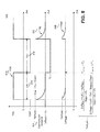
- the solid curve 678 bottom left in FIG. 6 12 shows an exemplary characteristic of a collector-emitter voltage of an IGBT (an IGBT is an exemplary power semiconductor switch) during the switching process from a switched-off state to a switched-on state (the course of an associated exemplary control signal 630 is shown at the top left). As shown, the collector-emitter voltage drops sharply to a very low value (close to 0 volts). An exemplary short-circuit behavior of an IGBT is shown at the bottom right in FIG FIG. 6 shown (solid curve 678).
- the collector-emitter voltage does not drop to the very low value, but at the same time high currents can flow in the IGBT (for example, between three times and ten times the rated current of the IGBT).
- the collector-emitter voltage initially drops to the value in normal operation, but then increases again. This results in a high thermal load of the power semiconductor switch, which can take damage after a relatively short time. For example, some IGBTs withstand a short circuit for about 10 ⁇ s when switched on, without being damaged. Therefore, the protection circuits for detecting a short circuit or overcurrent condition in this time range can cause the power semiconductor switch to be turned off. Similar characteristics can be found in other power semiconductor switches except IGBTs.
- An overcurrent condition may manifest as a short circuit condition due to an increased collector-emitter voltage.
- the collector-emitter voltage can be closer to a collector-emitter voltage in the normal case than in the case of a short circuit.
- collector-emitter voltage threshold that is used to detect the presence of a short-circuit or over-current condition. For example, as the collector-emitter voltage rises above the threshold (see FIG. 6 bottom right) a short circuit or overcurrent condition can be detected.
- a first device for generating a dynamic reference signal for a control circuit for a power semiconductor switch comprises a reference signal generator for providing a dynamic reference signal, which has a stationary signal level after a predetermined time after a switching operation of the power semiconductor switch, a passive charging A circuit configured to increase a signal level of the dynamic reference signal in response to switching a control signal of the power semiconductor switch from an OFF state to an ON state for at least a portion of the predetermined time above the steady state signal level to produce the dynamic reference signal and an output for picking up the dynamic reference signal.
- the device of the invention can accomplish the increase of the level of the dynamic reference signal without active devices.
- the device can be cheaper and more robust than comparable devices with active components.
- the device can be designed with relatively little effort reliably and with a negligible temperature drift.
- FIG. 6 An exemplary course of a dynamic reference signal is in FIG. 6 shown lower left (dashed line 648).
- the level of the dynamic reference signal is increased abruptly in response to a switching of a control signal of the power semiconductor switch from an OFF state to an ON state, and then continuously decreases until the steady state level is reached again.
- This increased reference voltage following a switching from an off to an on state may be used in a protection circuit.
- the protection circuit does not trip because a collector-emitter voltage representative signal (U C'E ) always remains below the reference signal.
- the dynamic reference signal is a dynamic reference voltage.
- the power semiconductor switch is an IGBT.
- the passive charging circuit comprises an RC element.
- the passive charging circuit is designed so that the control signal of the power semiconductor switch can be coupled to a first terminal of a capacitance of the RC element and a second terminal of the capacitance of the RC element directly or indirectly to the Output for tapping the dynamic reference signal is coupled.
- the passive charging circuit is configured to jump-increase the signal level of the dynamic reference signal in response to the switching of the control signal.
- the passive charging circuit is further designed so that the capacitance of the RC element after switching a control signal of the power semiconductor switch from an on state to an off state loads.
- the passive charging circuit is designed so that the capacity of the RC element discharges following the switching of the control signal and thus the second-wise increased level of the dynamic Generated reference signal and returned by the discharge back to the stationary level.
- a 1 / e time constant of the RC element is larger than 1 ⁇ s.
- a 1 / e time constant of the RC element is between 5 and 15 ⁇ s.
- the reference signal generator includes a circuit for generating the steady state signal level.
- the stationary signal level generating circuit includes one or more resistors and an input for receiving a constant current, the stationary signal level generating circuit configured to pass the constant current through the one or more resistors. such that across the one or more resistors, a steady state reference voltage drops to produce the steady state signal level.
- the one or more resistors are coupled to a first internal reference level.
- the first internal reference level corresponds to an emitter voltage, a cathode voltage, or a source voltage of the power semiconductor switch.
- the device further comprises a first clamp circuit configured to limit the dynamic reference voltage to a predetermined minimum level.
- the minimum level corresponds to an emitter voltage, a cathode voltage, or a source voltage of the power semiconductor switch.
- the minimum level is less than or equal to the stationary signal level.
- the device further comprises a second clamp circuit configured to limit the dynamic reference voltage to a predetermined maximum level.
- the maximum level corresponds to a signal level of the control signal in the ON state.
- the device further comprises a passive switch coupled between the reference signal generator and the passive charging circuit, the passive switch being adapted to the reference signal generator and the passive charging circuit in response to switching the control signal of the power semiconductor switch from an on state to an off state.
- the predetermined time is between 4 and 25 ⁇ s.
- the predetermined time is between 8 and 15 ⁇ s.
- the passive charging circuit is adapted to adjust a signal level of the dynamic reference signal in response to a switching of a reference signal To increase the control signal of the power semiconductor switch from an OFF state to an ON state for the entire predetermined time above the stationary signal level for generating the dynamic reference signal.
- the dynamic reference signal is a voltage signal.
- the dynamic reference signal is a current signal.
- the stationary signal level generating circuit comprises an input for receiving a constant voltage.
- an internal reference level of the device constitutes the steady-state signal level.
- a first control circuit for a power semiconductor switch comprises an apparatus for generating a dynamic reference signal for a control circuit for a power semiconductor switch according to any one of the first to twenty-sixth apparatuses, a short circuit and / or overcurrent condition detecting circuit which receives a dynamic reference signal from the apparatus for generating a dynamic reference signal and a signal representative of a collector-emitter voltage, a signal representative of an anode-cathode voltage or a signal representative of a drain-source voltage of the power semiconductor switch and configured to compare the dynamic reference signal with the signal representative of a collector-emitter voltage, for an anode-cathode voltage or for a drain-source voltage to produce an error signal, a presence of a K short circuit and / or overcurrent state in the power semiconductor switch and a driver circuit, the Error signal and is adapted to turn off the power semiconductor switch when the error signal indicates the presence of a short circuit and / or overcurrent condition in the power semiconductor switch.
- the short circuit and / or overcurrent condition detection circuit indicates the presence of a short circuit and / or overcurrent condition in the power semiconductor switch when the signal, for a collector-emitter voltage, for an anode cathodes Or in a third control circuit according to the first or second control circuit and that of one of the eleventh to thirteenth devices, the drive circuit further comprises the current source for generating the constant current.
- a first device for providing electrical energy comprises one or more inputs for connection to a source of electrical energy, one or more outputs for connection of one or more loads, one of the first to third control circuits, and a power semiconductor switch controlled by the control circuit, wherein the device is adapted to transfer electrical energy by controlling the power semiconductor switch from the one or more inputs to the one or more outputs.
- the power semiconductor switch is an IGBT or a reverse blocking IGBT.
- the power semiconductor switch is a GTO, an IEGT, a MOSFET or a bipolar transistor.
- the capacitance of the RC element discharges with a time constant selected to prevent the short circuit and / or overcurrent condition detection circuit from detecting a short circuit and / or overcurrent condition during normal operation.
- the capacitance of the RC member discharges with a time constant that is selected to ensure that the shorting and discharging capacitances are discharged / or overcurrent condition detection circuit detects a short circuit and / or overcurrent condition in the event of a short circuit and / or overcurrent.
- the control circuit further comprises a second power semiconductor switch, a second control circuit for the second power semiconductor switch, the second control circuit comprises a second device for generating a dynamic reference signal a control circuit for the second power semiconductor switch according to any one of the apparatuses 1 to 25, a second short circuit and / or overcurrent condition detection circuit comprising a dynamic reference signal from the second dynamic reference signal generating means and a signal representative of a collector-emitter Voltage representative, or a signal representative of a collector-emitter voltage, for an anode-cathode voltage or for a drain-source voltage of the power semiconductor switch is representative and configured to compare the dynamic reference signal with the signal representative of a collector-emitter voltage, for an anode-cathode voltage or for a drain-source voltage to produce a second error signal Short circuit and / or overcurrent state in the second power semiconductor switch and a second driver circuit which receives the second error signal and to is configured to
- a seventh apparatus for providing electrical energy the first and second power semiconductor switches are connected in series, and the apparatus is configured to couple a load between the first and second power semiconductor switches, and one Input voltage across the series-connected first and second power semiconductor switches is applied.
- the first and second power semiconductor switches are configured to carry a voltage between 100 V and 15 kV.
- a method for generating a dynamic reference signal for a power semiconductor switch comprising generating a stationary reference signal, receiving a control signal of the power semiconductor switch, increasing a level of the stationary reference signal in response to switching a control signal of the power semiconductor switch of FIG an OFF state to an ON state for at least a part of the predetermined time using a passive circuit and outputting dynamic reference signal.
- the time until a static state is reached be relatively long (eg significantly longer than 10 microseconds).
- a static reference voltage which is set near a specific static forward voltage of the power semiconductor switch, can thus also lead to the fact that the protective circuit erroneously assumes a short circuit and / or overcurrent case and the Power semiconductor switch turns off.
- the protection circuit may detect a dangerously increased voltage, although the voltage level increased at a certain time is only attributable to the inertia of the power semiconductor switch.
- Fig. 1 shows a device 100 (also referred to as a power converter) for providing electrical energy to a consumer 110.
- element 110 is a producer.
- element 110 may operate in various operating states both as a consumer and as a generator.
- the device comprises two power semiconductor switches 104, 106 which are connected in series.
- device 100 may receive a DC input voltage 102 (U IN ).
- U IN DC input voltage
- the device is configured to transfer electrical energy by controlling the power semiconductor switches 104, 106 from the input to an output to which the load 110 is connected (or in the reverse direction).
- the device for supplying electrical energy can control voltage levels, current levels or a combination of the two variables that are delivered to the consumer.
- the power semiconductor switches 104, 106 IGBTs are the power semiconductor switches 104, 106 IGBTs.
- the devices and methods will be explained using the example of IGBTs.
- the devices for generating a dynamic reference signal, the control circuits and the inventive devices for providing electrical energy are not limited to use with IGBTs. Rather, they can also be used in combination with other power semiconductor switches.
- MOSFETs metal oxide semiconductor field effect transistor
- IEGTs injection enhancement gate transistors
- GTOs gate turn-off thyristors
- the devices for Detecting a waveform of a voltage across a power semiconductor switch using control circuits and the electrical power supply devices with power semiconductor switches based on gallium nitride (GaN) or silicon carbide (SiC) semiconductors may be more than 500 V, preferably more than 2 kV.
- the devices for generating a dynamic reference signal, the control circuits and the inventive devices for providing electrical energy are not limited to power semiconductor switches.
- other semiconductor switches may be used with the devices for detecting a voltage across a power semiconductor switch, the control circuits and the devices for providing electrical energy.
- the effects and advantages discussed herein occur, at least in part, in systems with other semiconductor switches.
- the terminals of the power semiconductor switch are referred to as "collector,” “gate,” and “emitter.”
- the devices and methods are not limited to IGBTs.
- the term “emitter” herein also includes the connection of corresponding power semiconductor switches, referred to as "source” or "cathode”.
- collector herein also includes the terminal labeled “drain” or “anode” and the term “gate” includes the terminal labeled “base” of corresponding power semiconductor switches.
- collector-emitter voltage also includes a “drain-source voltage” and a “cathode-anode voltage” and the terms “collector voltage” and “emitter voltage” also include a “drain-source voltage”. Voltage "or” anode voltage “or a” source voltage "or” cathode voltage ".
- the power semiconductor switches 104, 106 are respectively controlled by first and second control circuits 118, 120 (an exemplary control circuit will be described in connection with FIG Fig. 2 illustrated). These provide first and second gate emitter drive signals 130, 132 (U GE1 , U GE2 ) ready to control the switching times of the first and second IGBTs. Both control circuits 118, 120 may optionally be controlled by a system controller 114.
- the system controller 114 may include an input for receiving system input signals 116.
- two power semiconductor switches 104, 106 are shown in a half-bridge configuration. However, the devices for generating a dynamic reference signal, the control circuits and the devices for providing electrical energy can also be used in other topologies.
- a single power semiconductor switch (eg, a single IGBT) may be connected to a device for generating a dynamic reference signal or a control circuit.
- each of the power semiconductor switches may include a device for generating a dynamic reference signal.
- the control circuits 118, 120 receive signals representing voltages applied across the power semiconductor switches 104, 106. The signals may be voltage signals or current signals.
- Each control circuit 118, 120 each has a signal representative of the collector-emitter voltage, referred to as collector-emitter voltage signal 122, 124 (U CE1 , U CE2 ).
- a current through the power semiconductor switch (eg, a collector current, a drain current, or a cathode current) may be otherwise estimated or measured directly.
- a device also referred to as a power converter
- a detection circuit for directly measuring a current through a power semiconductor switch (eg, a collector current measuring device).
- control circuits 118, 120 are outlined as separate control circuits. However, both control circuits 118, 120 may also be combined in a single circuit. In this case, a single control circuit controls two power semiconductor switches 104, 106.
- the second gate emitter drive signal 132 (U GE2 ) may be an inverted first gate emitter drive signal 130 (U GE1 ).
- Both control circuits 118, 120 comprise a device for generating a dynamic reference signal. With their help, based on the respective collector-emitter voltage signal 122, 124, a short-circuit and / or overcurrent state of the respective power semiconductor switch can be determined. In response to detection of a short circuit and / or overcurrent condition, the respective power semiconductor switch 104, 106 may be turned off.
- control circuit 218 is illustrated (eg, one of the control circuits 118, 120) Fig. 1 ).
- the control circuit 218 includes four functional units: a dynamic reference signal generator 242, a short circuit and / or overcurrent condition detector circuit 240, a driver circuit 236 and an optional driver interface 234.
- the dynamic reference signal generator 242 is adapted to operate Gate emitter drive signal 230 from the driver circuit 236 to receive.
- a device for generating a dynamic reference signal 242 may also receive other signals representative of the gate-emitter drive signal 230.
- the device for generating a dynamic reference signal 242 is optionally configured to receive an external reference signal.
- the external reference signal may be a reference signal 226 that is representative of the emitter voltage of a power semiconductor switch.
- voltage levels other than an external reference signal offset by a constant offset from the emitter voltage of a power semiconductor switch may be used.
- the dynamic reference signal generating device 242 is configured to receive a constant current signal 246 (I 1 ).
- the constant current signal 246 is provided by the driver circuit 236.
- the constant current signal 246 may alternatively be provided by other functional units of the control circuit 218, or may also be provided by an external source or generated internally by the circuit for generating the reference signal itself.
- any suitable source of current comes into consideration.
- the dynamic reference signal generator 242 Based on the received signals (ie, constant current signal 246 and gate emitter drive signal 230), the dynamic reference signal generator 242 provides a dynamic reference signal 248. This is received by the short circuit and / or overcurrent condition detection circuit 240.
- the dynamic reference signal 248 has a steady state signal level after lapse of a predetermined time after a switching operation of the power semiconductor switch.
- the dynamic reference signal 248 is raised above the steady state signal level at least in a portion of a period from the switching operation of the power semiconductor switch to the elapse of the predetermined time.
- the steady-state signal level of the dynamic reference signal does not have to be the same in all operating situations. Thus, a drift or a slow change in the steady state signal level relative to a length of a switching cycle is possible.
- the stationary signal level can be adjustable.
- the short circuit and / or overcurrent condition detection circuit 240 is configured to receive a signal 222 corresponding to the collector-emitter voltage U CE of a power semiconductor switch (eg, signals 122 or 124 off Fig. 1 ). Based on this signal 222, which corresponds to the collector-emitter voltage of the power semiconductor switch, the short-circuit and / or over-current state detection circuit 240 detects a signal representative of a collector-emitter voltage across the power semiconductor switch (U C'E ). , In other examples, the short circuit and / or overcurrent condition detection circuit 240 determines this signal from other signals or receives a signal representative of a collector-emitter voltage across the power semiconductor switch from another circuit block.
- the short circuit and / or overcurrent condition detection circuit 240 receives a signal representative of a current through the power semiconductor switch (eg, for a collector current).
- the signal representative of a current through the power semiconductor switch may be generated by a direct measurement of the current through the power semiconductor switch.
- the short circuit and / or overcurrent condition detection circuit 240 may then compare the signal representative of a current through the power semiconductor switch to the dynamic reference signal to detect a presence of a short circuit and / or overcurrent condition in the power semiconductor switch.
- Exemplary waveforms of a signal representative of a current through the power semiconductor switch are shown in FIG Fig. 6 shown below (using the collector current I C ' as an example). It can also be seen there that the normal and short-circuit and / or overcurrent states can be detected indirectly, both directly by a characteristic change in the course of the current, and indirectly by a characteristic change in the course of the voltage.
- the short-circuit and / or overcurrent condition detection circuit 240 In response to the received or detected signal representative of a collector-emitter voltage across the power semiconductor switch (or a received or detected signal representative of the collector current through the power semiconductor switch) and the received dynamic reference signal 248, the short-circuit and / or overcurrent condition detection circuit 240, whether a short-circuit and / or overcurrent condition exists.
- the short circuit and / or overcurrent condition detection circuit 240 detects that there is a short circuit and / or overcurrent condition when the signal representative of the collector-emitter voltage (or the signal representative of the collector current through the collector current) is detected Power semiconductor switch is representative) is greater than the dynamic reference signal 248.
- the collector-emitter voltage (or the collector current) after switching on the power semiconductor switch should drop rapidly to a relatively low value and a collector-emitter voltage increased above this value.
- Emitter voltage (or an increased collector current) is an indirect (or direct) indicator of the presence of a short circuit and / or overcurrent condition.
- the lower curves in Fig. 6 illustrate this and the operation of the short circuit and / or overcurrent condition detection circuit 240.
- FIG Fig. 6 On the left side of FIG Fig. 6 a normal switch-on process is shown.
- the voltage U C'E (in this case, the signal representative of the collector-emitter voltage) drops rapidly after the switching operation.
- the current I C ' (in this case, the signal representative of the collector current) also rapidly reaches a more or less steady state level.
- the dynamic reference signal is always above the signal U C'E 678 (or above a signal representative of the collector current) so that no short circuit and / or overcurrent condition is detected.
- the temporary increase of the level of the dynamic reference signal after the switching operation can prevent an erroneous detection of a short circuit and / or overcurrent condition.
- Fig. 6 On the right side down in Fig. 6 however, is a typical waveform of the signal representative of the collector-emitter voltage and outlines the waveform of the signal representative of the collector current in a short circuit and / or overcurrent case.
- the signal U C'E 678 and the signal I C ' exceed the dynamic reference signal (eg, after 8 to 12 ⁇ s after a switching operation) and so the short circuit and / or overcurrent condition detection circuit 240 has a short circuit and /or
- the dynamic reference signal is increased for at least a portion of a predetermined time (e.g., the entire predetermined time) so that no fault is detected if voltage spikes and voltage valleys occur after the power semiconductor switch is turned on during the predetermined time, or the complete one Decreasing of the collector-emitter voltage representative signal to a low value below the static reference signal generally lasts longer than the maximum permissible short-circuit duration for the power semiconductor switch is defined.
- the duration of the increase of the dynamic reference signal can be adjusted to minimize the frequency of occurrence of false error detections. As in Fig.
- the overcurrent condition detection circuit 240 may, when it has detected a short circuit and / or overcurrent condition, output an error signal.
- an error signal 244 (U FT ) is output to the driver circuit 236. This may turn off the power semiconductor switch in response to the error signal 244 to prevent damage thereto.
- the error signal may be processed in other ways. For example, only the error signal 250 (U FT ) may be provided to another control (eg, to the system controller 214). This further element may then turn off two or more power semiconductor switches in a predetermined sequence.
- the short circuit and / or overcurrent condition detection circuit 240 may further process the received signals.
- the short circuit and / or overcurrent condition detection circuit 240 may include a blanking circuit to to set a predetermined delay in the detection of a short circuit and / or overcurrent condition.
- the short circuit and / or overcurrent condition detection circuit 240 may include a circuit for adjusting a voltage level of the signal representative of the collector-emitter voltage (or a signal representative of the collector current of the power semiconductor switch) , Since the collector-emitter voltage itself can be several thousand volts or more, this circuit may comprise a network of high-resistance resistors.
- the network may also contain other elements designed for high voltages (eg capacitive components or diodes). This produces from the collector-emitter voltage a signal proportional to the collector-emitter voltage but having a (much) lower voltage level (e.g. Fig. 6 sketched signal U C'E ).
- the driver circuit 236 may receive an error signal 244 indicative of a short circuit and / or overcurrent condition and turn off the power semiconductor switch in response to a detected short circuit and / or overcurrent condition.
- One or more components of the short circuit and / or overcurrent condition detection circuit 240 may optionally be included in the driver circuit 236.
- the driver circuit 236 may receive the dynamic reference signal U REF 248 and the signal representative of the collector-emitter voltage (or a signal representative of the collector current through the power semiconductor switch).
- the driver circuit 236 may also provide a gate emitter drive signal for controlling the power semiconductor switch.
- FIG. 10 is an exemplary apparatus for generating a dynamic reference signal 342 (eg, block 242 in FIG Fig. 2 ) for a control circuit for a power semiconductor switch.
- the device for generating a dynamic reference signal 342 includes two functional blocks, a reference signal generator 352 and a passive load circuit 350. The function of these blocks will be explained below.
- the exemplary circuit is not limited to cases in which the functions explained below are performed in separate units. Rather, a part or all functions of a block can also be implemented together.
- the dynamic reference signal generating device 342 receives a control signal of the power semiconductor switch 330 (U GE ), and a constant current signal 346 (I 1 ).
- the devices for generating a dynamic reference signal receive a constant current signal.
- the devices for generating a dynamic reference signal receive a constant voltage signal.
- the control signal of the power semiconductor switch 330 may be any signal representing the timing of the switching operations of the power semiconductor switch.
- the gate drive signal can be used.
- a suitable signal may also be present at other locations in order to provide the device for generating a dynamic reference signal 342 with information about the switching operations of the power semiconductor switch.
- the constant current signal 346 (or a constant voltage signal) may also be generated in the dynamic reference signal generating device 342 itself.
- the reference signal generator 352 of the dynamic reference signal generating device 342 provides a dynamic reference signal 348 (U REP or I REF ) having a steady state signal level after a lapse of a predetermined time after a switching operation of the power semiconductor switch.
- the reference signal generator 352 may include one or more components for generating the steady state signal level in response to the constant current signal 346 (or a constant voltage signal).
- Examples of the reference signal generator 352 are shown in conjunction with FIGS. 4A, 4B and 7 .
- the passive charging circuit 350 is configured to adjust one signal level of the dynamic reference signal in response to switching a control signal of the power semiconductor switch from an OFF state to an ON state for at least a part of the predetermined time (for example, for the entire predetermined time Time) above the steady-state signal level to produce a dynamic reference signal.
- the passive charging circuit 350 receives the control signal U GE 330.
- the control signal U GE 330 is processed by the passive charging circuit 350 to determine the timing of the switching operation of a control signal of the power semiconductor switch from a turned-off state to a turned-on state.
- the amplitude and timing may increase the reference dynamic signal above the steady state signal level based at least in part on the control signal U GE 330 be determined.
- This temporary increase of the dynamic reference signal accomplishes the passive charging circuit 350 without active devices (such as transistors).
- Exemplary passive charging circuits 350 are again associated with FIG Fig. 4A . Fig. 4B and Fig. 7 shown.
- the passive charging circuit 350 is configured to adjust the timing of the temporary increase of the dynamic reference signal as in FIG Fig. 6 represented at least partially controlled. This includes an abrupt increase in response to switching a control signal of the power semiconductor switch from an OFF state to an ON state followed by a continuous decrease back to the level of the steady state voltage signal.
- the time constant (1 / e time constant) of the decrease can be between 1 and 50 ⁇ s (eg between 5 and 15 ⁇ s).
- the passive charging circuit 350 may include an RC element, wherein the time constant of a capacitance of the RC element is the speed of sinking to levels of the stationary Voltage signal determined at least partially.
- the increase in the level of the dynamic reference signal 348 above the level of the static reference signal may correlate to a jump in the amplitude of the control signal U GE 330. In connection with Fig. 6 Exemplary signal levels are explained.
- FIG. 12 shows a first example of a device for generating a dynamic reference signal 442.
- the device includes a reference signal generator 452 and a passive load circuit 450.
- the device receives a dynamic reference signal 442 as in the example of FIG Fig. 3 , a control signal of the power semiconductor switch 430 (U GE ), a constant current signal 446 (I 1 ).
- U GE control signal of the power semiconductor switch 430
- I 1 constant current signal
- Reference signal generator 452 includes a circuit for generating a static reference signal.
- the circuit for generating a static reference signal includes a reference resistor 464 (R REF ).
- the constant current signal 346 is coupled to a first terminal of the reference resistor 464, flows through the reference resistor 464, thus producing a constant voltage drop (I 1 * R REF ). Even if in Fig. 4A the reference resistor 464 is shown as a single component, a combination of a plurality of resistors can also be used.
- a constant voltage source may be employed in the devices to generate a dynamic reference signal (rather than generating them by the fall in the constant current I 1 across the reference resistor R REF 464).
- a constant voltage source may be connected in series with reference resistor R REF 464 (to some extent in place of VI).
- the constant voltage source may be connected between the reference resistor R REF and V E.
- an internal reference level already present in the devices for generating a dynamic reference signal may form the static voltage reference level (eg, the internal reference level 447 (V 1 )).
- the internal reference level can be replaced by a passive one Semiconductor circuit (eg with a Zener diode) are generated.
- the reference resistor R REF 464 may be omitted. The devices for generating a dynamic reference signal then generates a reference current I REF (instead of a reference voltage U REF ).
- the dynamic reference signal generating device 442 generates a first internal reference level 447 (V 1 ).
- the first internal reference level 447 (V 1 ) may be generated based on the reference level 426 or correspond to it.
- the first internal reference level 447 is substantially equal to the emitter voltage of the power semiconductor switch. This is advantageous because typically in short circuit and / or overcurrent condition detection circuits (see block 240 in FIG Fig. 2 ) also a reference signal representative of the emitter voltage is used. Thus, in this case, both a collector-emitter voltage signal and a dynamic reference signal, which are compared with each other, are referenced to the same signal. This can facilitate the mutual stabilization of the signals. Nonetheless, for the first internal reference level 447 (V 1 ), any level below the static voltage reference level is usable.
- the node A of the reference signal generator 452 which is connected to an output for the output of the dynamic reference signal 448, is thus raised by the circuit for generating the stationary signal level to a stationary signal level.
- the dynamic reference signal 448 (U REF ) is a dynamic voltage signal.
- a dynamic current signal can be used.
- This stationary signal level is in the exemplary device according to Fig. 4A V 1 + R REF * I 1 .
- the level of the dynamic reference signal 448 corresponds to the steady state signal level (ie, V 1 + R REF * I 1 ).
- This behavior is in Fig. 5A shown.
- the lowermost curve represents an exemplary waveform of the voltage at node A (and thus the dynamic reference signal 548). It can be seen that the voltage level at node A is stationary except for certain times following the switchings of the semiconductor switch.
- the passive charging circuit 450 via resistor 466 (R 1 ) is connected (this is in Fig. 4A drawn as belonging to the reference signal generator 452, which however is an arbitrary division).
- the passive charging circuit 450 includes an RC element. This includes a capacitance 456 (C T ) and a resistor 460 (R T ).
- the capacitor 456 is coupled between a node B and an input receiving the control signal of the power semiconductor switch 430.
- the resistor 460 is coupled between the node B and the node A of the reference signal generator 452.
- the resistors 460 and 466 may also be a single resistor.
- the passive charging circuit 450 includes an optional first clamp circuit 454 which limits a voltage level at the node B to a second internal reference level 462 (V L ).
- the first clamp circuit 454 includes a diode 454.
- the second internal reference level 462 may be any level less than or equal to the static voltage reference level. When the external reference level 426 satisfies this condition, it may be used as the second internal reference level 462. Again, the second internal reference level 462 may be representative of the emitter voltage of the semiconductor power switch.
- the passive charging circuit 450 contains no active components.
- the device for generating a dynamic reference signal 442 immediately prior to a switching operation outputs a dynamic reference voltage which substantially corresponds to the internal reference level 447 plus the voltage generated across resistor R REF 464 of constant current 446 (I 1 * R REF + V 1 in the device of Fig. 4A ).
- the dynamic reference voltage 448 equals the steady state voltage level.
- the topmost curve of Fig. 5A shows an exemplary course of a control signal 530 (U GE ) of the power semiconductor switch.
- the voltage level of the control signal 530 rises from a level in the off state V OFF to a level in the on state V ON .
- the V OFF and V ON levels of the gate-emitter voltage of the power semiconductor switch that controls the power semiconductor switch are in the off state.
- an off-level V OFF for IGBTs may be between -20V and -5V (preferably between -15V and -7V), and an on-level V ON may be between 10V and 20V for IGBTs (preferably between 13V and 15V) ).
- the levels V OFF and V ON may correspond to the voltage of the gate-source voltage of the power MOSFET in the off state.
- an off-level V OFF for power MOSFETs may be between -5V and 0V, and an on-level V ON may be between 10V and 25V for MOSFETs.
- a level in the off state V OFF may also be between -5V and 0V, and a level in the on state V ON may be between 10V and 20V.
- the amplitude of the voltage jump thus corresponds to the difference between the level in the switched-on state V ON and the level in the switched-on state V OFF of the control signal 530 (430 in FIG Fig. 4A ).
- a voltage level V Bpeak of V Bpeak V ON + I 1 ⁇ R REF + V 1 - V OFF ,
- the additional current discharges the capacitance 456 of the passive charging circuit 450.
- a voltage across the capacitance 454 decreases, and consequently, the voltage level at node B also decreases.
- the additional current decreases and also the voltage at node A decreases (and thus the level of the dynamic reference signal 448).
- the capacitance has discharged so far that no additional current is driven through the resistor 464.
- the voltage at node A is again at its steady state level (of I 1 * R REF + V 1 ).
- the temporary increase of the dynamic reference signal generated by the passive charging circuit has decayed.
- the time constant of the discharge of the capacitor 456 is determined by the values of the resistors 460 (R T ), 466 (R 1 ) and 464 (R REF ) and the value of the capacitance 456 (C T ). It and the amplitude of the voltage swing in dynamic reference signal 448 may be selected to prevent or at least reduce erroneous detections of a short circuit and / or overcurrent condition after a switch from an off state to a on state of the power semiconductor switch Nevertheless, a protective function is achieved by a safe shutdown of the power semiconductor switch. This can in turn be based on Fig. 6 to be illustrated.
- the temporary increase of the dynamic reference signal 648 ensures that the signal representative of the collector-emitter voltage is normally (left side in FIG Fig. 6 ) is below the dynamic reference signal.
- the short circuit and / or overcurrent condition detection circuit 240 in FIG Fig. 2 So would not detect a short circuit and / or overcurrent condition.
- Fig. 5A the behavior of the device for generating a dynamic reference signal 442 after a switching operation from an on state to an off state of the power semiconductor switch is shown.
- the reverse process occurs as in the case of the switchover from the off state to the on state described above.
- a negative, in this case negative, voltage swing of the control signal 530 is applied to the first input of the capacitor 454 and reduces the voltage at the node B. This in turn results in an additional current which reduces the voltage at the node A.
- the first clamp 454 is now active and limits the voltage drop at node B to the second internal reference level V L.
- the first clamping circuit 454 is optional, the device for generating a dynamic reference signal 442 may also be used without it. Then, the dynamic reference signal 448 would be reduced by the full voltage swing of the control signal 430. However, this can be detrimental because the voltage at node A (the dynamic reference signal 448) and the voltage at node B may not have enough time to return to the steady state signal level.
- V Aclamp I 1 ⁇ R REF + V 1 ⁇ R 1 + R T + V L ⁇ R REF R REF + R 1 + R T
- Fig. 4B shows a second example of a device for generating a dynamic reference signal.
- the structure corresponds to that of Fig. 4A shown device, in addition to a second clamping circuit 468, 470 is provided. This is designed to limit the dynamic reference voltage 448 to a predetermined maximum value.
- the maximum value of the dynamic reference voltage 448 is set by a third internal reference level V H.
- the second clamp circuit 468, 470 may include a second diode 468.
- the third internal reference level V H is chosen to prevent damage to devices to which the dynamic reference signal generating device 442 is connected. For example, as in Fig.
- the constant current I 1 supplied by the driver circuit 236 Since dynamic reference signal 448 is applied to the reference output of driver circuit 236, it may be damaged by the increased voltage level of dynamic reference signal 448.
- the maximum allowable voltage at the reference output of driver circuit 236 may correspond to V ON . In other environments, the maximum allowable voltage may be higher, so a limitation by means of the second clamping circuit 468 is not absolutely necessary.
- the course of the temporary increased dynamic reference signal 448 in the device according to Fig. 4B is in Fig. 5B outlined.
- the profile of the voltage level at node B in the devices according to Fig. 4A and Fig. 4B are identical.
- the course of the temporary reduction of the dynamic reference signal 548 below its stationary level corresponds to that in FIG Fig. 5A outlined.
- a difference can be seen in the switching process from a switched-off state to a switched-on state of the power semiconductor switch.
- the dynamic reference signal is first clamped to the value given in Equation 4 until diode 468 of the second clamp circuit stops conducting. Thereafter, the dynamic reference voltage 548 drops back to its steady state signal level.
- Equation 4 diode 468 of the second clamp circuit stops conducting.
- FIG. 7 is a third example of a device for generating a dynamic reference signal 742.
- the device corresponds to the in Fig. 4B as shown, with the exception that a third diode 772 (D 3 ) is disposed between the second clamp circuit 768, 570 and the resistor 760 (R T ).
- the third diode 772 (D 3 ) influences the behavior of the device for generating a dynamic reference signal 742 after a switching operation of the power semiconductor switch from a switched to a switched-off state.
- the waveforms of the voltage levels at node A (corresponding to dynamic reference signal 848) and the voltage level at node B 855 after turn-on correspond to those in FIG Fig. 5B shown.
- the behavior of the devices for generating a dynamic reference signal differs according to Fig. 4B and Fig. 8 However.
- the diode 772 (D 3 ) turns off.
- the reference signal generator 752 is decoupled from the passive load circuit 752. That has In turn, a drop in the voltage level at node A below the steady-state voltage level (and thus also dynamic reference signal 748) can be prevented or significantly reduced.
- the voltage level at node A very quickly returns to its static level (V 1 + I 1 * R REF ), since this process is no longer coupled to the discharge behavior of the capacitance 756 of the RC element of the passive charging circuit 750.
- the capacitance is discharged to this value via R T , R 1 and R REF , resulting in the dynamic increase of the dynamic reference voltage U REF .
- the second internal reference level 762 (VL) is lower than I 1 * R REF + V 1 , the diode 772 (D3) turns off.
- the capacitance 756 (C T ) is not additionally reloaded over this path.
- This behavior is in curve 848 in Fig. 8 shown, the timing of the dynamic reference signal in the device according to Fig. 8 shows.
Landscapes
- Physics & Mathematics (AREA)
- Nonlinear Science (AREA)
- Electronic Switches (AREA)
- Power Conversion In General (AREA)
- Protection Of Static Devices (AREA)
Priority Applications (6)
| Application Number | Priority Date | Filing Date | Title |
|---|---|---|---|
| EP14172012.8A EP2955849A1 (fr) | 2014-06-11 | 2014-06-11 | Dispositif de fabrication d'un signal de référence dynamique pour un circuit d'excitation pour un disjoncteur à semi-conducteur |
| CN201580031529.2A CN106416072B (zh) | 2014-06-11 | 2015-06-11 | 为用于半导体功率开关的驱动电路产生动态基准信号的装置和方法 |
| JP2016572391A JP6955336B2 (ja) | 2014-06-11 | 2015-06-11 | 半導体電力スイッチ用の駆動回路のための動的基準信号を生成する装置および方法 |
| US15/313,488 US10171071B2 (en) | 2014-06-11 | 2015-06-11 | Device and method for producing a dynamic reference signal for a driver circuit for a semiconductor power switch |
| PCT/EP2015/063060 WO2015189332A1 (fr) | 2014-06-11 | 2015-06-11 | Dispositif et procédé pour générer un signal de référence dynamique pour un circuit de pilotage pour un disjoncteur de puissance à semi-conducteur |
| JP2020180173A JP7057810B2 (ja) | 2014-06-11 | 2020-10-28 | 半導体電力スイッチ用の駆動回路のための動的基準信号を生成する装置および方法 |
Applications Claiming Priority (1)
| Application Number | Priority Date | Filing Date | Title |
|---|---|---|---|
| EP14172012.8A EP2955849A1 (fr) | 2014-06-11 | 2014-06-11 | Dispositif de fabrication d'un signal de référence dynamique pour un circuit d'excitation pour un disjoncteur à semi-conducteur |
Publications (1)
| Publication Number | Publication Date |
|---|---|
| EP2955849A1 true EP2955849A1 (fr) | 2015-12-16 |
Family
ID=50942575
Family Applications (1)
| Application Number | Title | Priority Date | Filing Date |
|---|---|---|---|
| EP14172012.8A Withdrawn EP2955849A1 (fr) | 2014-06-11 | 2014-06-11 | Dispositif de fabrication d'un signal de référence dynamique pour un circuit d'excitation pour un disjoncteur à semi-conducteur |
Country Status (5)
| Country | Link |
|---|---|
| US (1) | US10171071B2 (fr) |
| EP (1) | EP2955849A1 (fr) |
| JP (2) | JP6955336B2 (fr) |
| CN (1) | CN106416072B (fr) |
| WO (1) | WO2015189332A1 (fr) |
Families Citing this family (10)
| Publication number | Priority date | Publication date | Assignee | Title |
|---|---|---|---|---|
| US10291225B2 (en) * | 2016-10-07 | 2019-05-14 | Texas Instruments Incorporated | Gate driver with VGTH and VCESAT measurement capability for the state of health monitor |
| DE102017108769B4 (de) * | 2017-04-25 | 2019-04-18 | Semikron Elektronik Gmbh & Co. Kg | Steuereinrichtung für einen Leistungshalbleiterschalter |
| EP3496348B1 (fr) | 2017-12-05 | 2020-10-14 | Power Integrations Switzerland GmbH | Communications faisant appel à un couplage inductif |
| EP3534538A1 (fr) * | 2018-02-28 | 2019-09-04 | LEM Intellectual Property SA | Module de commande de commutateur de puissance électronique |
| EP3696558A1 (fr) * | 2019-02-15 | 2020-08-19 | Siemens Aktiengesellschaft | Dispositif et procédé de vérification automatique d'un organe de commutation |
| US11146227B1 (en) * | 2019-09-06 | 2021-10-12 | Northrop Grumman Systems Corporation | Open-loop tracking control module to control input range swing for radiation-hardened devices |
| US10998843B2 (en) | 2019-09-23 | 2021-05-04 | Power Integrations, Inc. | External adjustment of a drive control of a switch |
| US11437911B2 (en) | 2020-12-22 | 2022-09-06 | Power Integrations, Inc. | Variable drive strength in response to a power converter operating condition |
| US11757351B2 (en) | 2021-07-30 | 2023-09-12 | Texas Instruments Incorporated | Dynamic overcurrent limit threshold for a voltage regulator |
| US11996795B2 (en) | 2022-03-28 | 2024-05-28 | Power Integrations, Inc. | Motor alignment control |
Citations (1)
| Publication number | Priority date | Publication date | Assignee | Title |
|---|---|---|---|---|
| US5453669A (en) * | 1993-06-04 | 1995-09-26 | Kabushiki Kaisha Tokai-Rika-Denki-Seisakusho | Motor current detection circuit |
Family Cites Families (11)
| Publication number | Priority date | Publication date | Assignee | Title |
|---|---|---|---|---|
| JPH0723525A (ja) * | 1993-06-30 | 1995-01-24 | Nec Corp | 過電流検出回路 |
| JP3706515B2 (ja) * | 1998-12-28 | 2005-10-12 | 矢崎総業株式会社 | 電源供給制御装置および電源供給制御方法 |
| JP3829534B2 (ja) * | 1999-05-26 | 2006-10-04 | 松下電工株式会社 | 放電灯点灯装置 |
| JP3800115B2 (ja) * | 2002-03-25 | 2006-07-26 | 株式会社デンソー | 過電流検出機能付き負荷駆動回路 |
| JP4961977B2 (ja) * | 2006-11-30 | 2012-06-27 | 株式会社デンソー | 過電流保護回路 |
| CN101534110A (zh) * | 2009-04-10 | 2009-09-16 | 深圳市科陆变频器有限公司 | 一种igbt限流驱动电路 |
| US20120235710A1 (en) * | 2011-03-15 | 2012-09-20 | Infineon Technologies Ag | Circuit Arrangement with a MOSFET and an IGBT |
| JP5726037B2 (ja) * | 2011-09-30 | 2015-05-27 | 三菱電機株式会社 | 半導体装置 |
| JP5959901B2 (ja) * | 2012-04-05 | 2016-08-02 | 株式会社日立製作所 | 半導体駆動回路および電力変換装置 |
| JP5947633B2 (ja) * | 2012-06-22 | 2016-07-06 | ローム株式会社 | 信号伝達回路、集積回路およびそれを含む電気機器 |
| JP5790606B2 (ja) * | 2012-08-20 | 2015-10-07 | 株式会社デンソー | 過熱保護回路 |
-
2014
- 2014-06-11 EP EP14172012.8A patent/EP2955849A1/fr not_active Withdrawn
-
2015
- 2015-06-11 CN CN201580031529.2A patent/CN106416072B/zh active Active
- 2015-06-11 US US15/313,488 patent/US10171071B2/en active Active
- 2015-06-11 JP JP2016572391A patent/JP6955336B2/ja active Active
- 2015-06-11 WO PCT/EP2015/063060 patent/WO2015189332A1/fr active Application Filing
-
2020
- 2020-10-28 JP JP2020180173A patent/JP7057810B2/ja active Active
Patent Citations (1)
| Publication number | Priority date | Publication date | Assignee | Title |
|---|---|---|---|---|
| US5453669A (en) * | 1993-06-04 | 1995-09-26 | Kabushiki Kaisha Tokai-Rika-Denki-Seisakusho | Motor current detection circuit |
Also Published As
| Publication number | Publication date |
|---|---|
| CN106416072B (zh) | 2020-09-01 |
| WO2015189332A1 (fr) | 2015-12-17 |
| JP2017519441A (ja) | 2017-07-13 |
| CN106416072A (zh) | 2017-02-15 |
| US20170187367A1 (en) | 2017-06-29 |
| US10171071B2 (en) | 2019-01-01 |
| JP7057810B2 (ja) | 2022-04-20 |
| JP6955336B2 (ja) | 2021-10-27 |
| JP2021036688A (ja) | 2021-03-04 |
Similar Documents
| Publication | Publication Date | Title |
|---|---|---|
| EP2884662B1 (fr) | Dispositifs et procédé de détection d'un état de court-circuit ou de surtension dans un commutateur de puissance à semi-conducteurs | |
| EP2955849A1 (fr) | Dispositif de fabrication d'un signal de référence dynamique pour un circuit d'excitation pour un disjoncteur à semi-conducteur | |
| EP3280052B1 (fr) | Procede et dispositif de commande d'un circuit semi-conducteur de puissance commande par tension | |
| DE112013006487B4 (de) | Ansteuervorrichtung für Halbleiterelemente und Halbleitervorrichtigung | |
| EP3057231B1 (fr) | Circuit de commande et procédé de commande destiné à commuter un interrupteur semi-conducteur de puissance | |
| EP0666647B1 (fr) | Procédé et circuit pour commander des commutateurs semi-conducteurs montés en série | |
| DE112017007140T5 (de) | Halbleitervorrichtung und Leistungsumwandlungssystem | |
| DE102012216318A1 (de) | Halbleitervorrichtung | |
| DE102015220594A1 (de) | Halbleiter-Antriebseinheit und Stromrichter, der diese verwendet | |
| DE112014004979B4 (de) | Halbleitervorrichtung | |
| DE102005045099A1 (de) | Entsättigungsschaltung für einen IGBT | |
| DE112015000270T5 (de) | Halbleitervorrichtung | |
| DE3335220A1 (de) | Phasenregelschaltung fuer eine niederspannungslast | |
| EP3711162B1 (fr) | Protection d'un transistor à effet de champ fonctionnant dans le mode de commutation contre un courant de surcharge | |
| DE102012224336A1 (de) | Verfahren zum Betreiben eines elektrischen Stromrichters sowie elektrischer Stromrichter | |
| EP2744110A1 (fr) | Circuit d'attaque et procédé destiné à la commande d'un circuit semi-conducteur de puissance | |
| EP0690898B1 (fr) | Circuit de protection contre les surtensions pour un commutateur semiconducteur de puissance pouvant être mis en circuit ou hors circuit | |
| EP3117511A1 (fr) | Procédé d'identification de l'effondrement d'une tension | |
| DE102013015723B3 (de) | Verbesserte Ansteuerung von Leistungshalbleitern | |
| DE102008025986A1 (de) | Überspannungsschutzvorrichtung für ein spannungsempfindliches Leistungshalbleiterbauteil | |
| DE102022129296A1 (de) | Diagnose einer Gatespannung, um einen hohen Strom zu Detektieren | |
| EP3857690B1 (fr) | Détection d'un courant de surcharge d'un commutateur électronique | |
| DE102015206031B4 (de) | Vorrichtung zum Begrenzen einer über einem Leistungsschalter abfallenden Spannung, Spannungszwischenkreisumrichter sowie Verfahren | |
| DE102010032717A1 (de) | Verfahren und elektrische Schaltung zum Betreiben eines Leistungshalbleiter-Bauelements | |
| DE19913455A1 (de) | Kurzschlußschutz für Leistungshalbleiterschalter |
Legal Events
| Date | Code | Title | Description |
|---|---|---|---|
| PUAI | Public reference made under article 153(3) epc to a published international application that has entered the european phase |
Free format text: ORIGINAL CODE: 0009012 |
|
| 17P | Request for examination filed |
Effective date: 20140611 |
|
| AK | Designated contracting states |
Kind code of ref document: A1 Designated state(s): AL AT BE BG CH CY CZ DE DK EE ES FI FR GB GR HR HU IE IS IT LI LT LU LV MC MK MT NL NO PL PT RO RS SE SI SK SM TR |
|
| AX | Request for extension of the european patent |
Extension state: BA ME |
|
| RAP1 | Party data changed (applicant data changed or rights of an application transferred) |
Owner name: POWER INTEGRATIONS SWITZERLAND GMBH |
|
| STAA | Information on the status of an ep patent application or granted ep patent |
Free format text: STATUS: THE APPLICATION IS DEEMED TO BE WITHDRAWN |
|
| 18D | Application deemed to be withdrawn |
Effective date: 20180103 |