EP2948979B1 - Kunststoffverpackung mit offenem hohlraum - Google Patents
Kunststoffverpackung mit offenem hohlraum Download PDFInfo
- Publication number
- EP2948979B1 EP2948979B1 EP14702428.5A EP14702428A EP2948979B1 EP 2948979 B1 EP2948979 B1 EP 2948979B1 EP 14702428 A EP14702428 A EP 14702428A EP 2948979 B1 EP2948979 B1 EP 2948979B1
- Authority
- EP
- European Patent Office
- Prior art keywords
- mold
- integrated circuit
- die
- pin
- plastic
- Prior art date
- Legal status (The legal status is an assumption and is not a legal conclusion. Google has not performed a legal analysis and makes no representation as to the accuracy of the status listed.)
- Active
Links
Images


Classifications
-
- B—PERFORMING OPERATIONS; TRANSPORTING
- B29—WORKING OF PLASTICS; WORKING OF SUBSTANCES IN A PLASTIC STATE IN GENERAL
- B29C—SHAPING OR JOINING OF PLASTICS; SHAPING OF MATERIAL IN A PLASTIC STATE, NOT OTHERWISE PROVIDED FOR; AFTER-TREATMENT OF THE SHAPED PRODUCTS, e.g. REPAIRING
- B29C45/00—Injection moulding, i.e. forcing the required volume of moulding material through a nozzle into a closed mould; Apparatus therefor
- B29C45/17—Component parts, details or accessories; Auxiliary operations
- B29C45/26—Moulds
- B29C45/2628—Moulds with mould parts forming holes in or through the moulded article, e.g. for bearing cages
-
- B—PERFORMING OPERATIONS; TRANSPORTING
- B81—MICROSTRUCTURAL TECHNOLOGY
- B81B—MICROSTRUCTURAL DEVICES OR SYSTEMS, e.g. MICROMECHANICAL DEVICES
- B81B7/00—Microstructural systems ; Auxiliary parts of microstructural devices or systems
- B81B7/0032—Packages or encapsulation
- B81B7/0058—Packages or encapsulation for protecting against damages due to external chemical or mechanical influences, e.g. shocks or vibrations
-
- H—ELECTRICITY
- H10—SEMICONDUCTOR DEVICES; ELECTRIC SOLID-STATE DEVICES NOT OTHERWISE PROVIDED FOR
- H10P—GENERIC PROCESSES OR APPARATUS FOR THE MANUFACTURE OR TREATMENT OF DEVICES COVERED BY CLASS H10
- H10P72/00—Handling or holding of wafers, substrates or devices during manufacture or treatment thereof
- H10P72/04—Apparatus for manufacture or treatment
- H10P72/0438—Apparatus for making assemblies not otherwise provided for, e.g. package constructions
-
- H—ELECTRICITY
- H10—SEMICONDUCTOR DEVICES; ELECTRIC SOLID-STATE DEVICES NOT OTHERWISE PROVIDED FOR
- H10W—GENERIC PACKAGES, INTERCONNECTIONS, CONNECTORS OR OTHER CONSTRUCTIONAL DETAILS OF DEVICES COVERED BY CLASS H10
- H10W74/00—Encapsulations, e.g. protective coatings
- H10W74/01—Manufacture or treatment
- H10W74/016—Manufacture or treatment using moulds
-
- B—PERFORMING OPERATIONS; TRANSPORTING
- B29—WORKING OF PLASTICS; WORKING OF SUBSTANCES IN A PLASTIC STATE IN GENERAL
- B29L—INDEXING SCHEME ASSOCIATED WITH SUBCLASS B29C, RELATING TO PARTICULAR ARTICLES
- B29L2031/00—Other particular articles
- B29L2031/34—Electrical apparatus, e.g. sparking plugs or parts thereof
- B29L2031/3481—Housings or casings incorporating or embedding electric or electronic elements
-
- H—ELECTRICITY
- H10—SEMICONDUCTOR DEVICES; ELECTRIC SOLID-STATE DEVICES NOT OTHERWISE PROVIDED FOR
- H10W—GENERIC PACKAGES, INTERCONNECTIONS, CONNECTORS OR OTHER CONSTRUCTIONAL DETAILS OF DEVICES COVERED BY CLASS H10
- H10W42/00—Arrangements for protection of devices
-
- H—ELECTRICITY
- H10—SEMICONDUCTOR DEVICES; ELECTRIC SOLID-STATE DEVICES NOT OTHERWISE PROVIDED FOR
- H10W—GENERIC PACKAGES, INTERCONNECTIONS, CONNECTORS OR OTHER CONSTRUCTIONAL DETAILS OF DEVICES COVERED BY CLASS H10
- H10W72/00—Interconnections or connectors in packages
- H10W72/50—Bond wires
- H10W72/551—Materials of bond wires
- H10W72/552—Materials of bond wires comprising metals or metalloids, e.g. silver
- H10W72/5522—Materials of bond wires comprising metals or metalloids, e.g. silver comprising gold [Au]
-
- H—ELECTRICITY
- H10—SEMICONDUCTOR DEVICES; ELECTRIC SOLID-STATE DEVICES NOT OTHERWISE PROVIDED FOR
- H10W—GENERIC PACKAGES, INTERCONNECTIONS, CONNECTORS OR OTHER CONSTRUCTIONAL DETAILS OF DEVICES COVERED BY CLASS H10
- H10W74/00—Encapsulations, e.g. protective coatings
- H10W74/10—Encapsulations, e.g. protective coatings characterised by their shape or disposition
-
- H—ELECTRICITY
- H10—SEMICONDUCTOR DEVICES; ELECTRIC SOLID-STATE DEVICES NOT OTHERWISE PROVIDED FOR
- H10W—GENERIC PACKAGES, INTERCONNECTIONS, CONNECTORS OR OTHER CONSTRUCTIONAL DETAILS OF DEVICES COVERED BY CLASS H10
- H10W90/00—Package configurations
- H10W90/701—Package configurations characterised by the relative positions of pads or connectors relative to package parts
- H10W90/751—Package configurations characterised by the relative positions of pads or connectors relative to package parts of bond wires
- H10W90/756—Package configurations characterised by the relative positions of pads or connectors relative to package parts of bond wires between a chip and a stacked lead frame, conducting package substrate or heat sink
Definitions
- the present disclosure relates to a method for manufacturing open cavity plastic packages for integrated circuits (ICs), in particular, using a cover over the IC die during the encapsulation process to provide a plastic package with an open cavity to allow the device to act as a sensing device.
- ICs integrated circuits
- Integrated circuits may include sensors for a variety of reasons.
- ICs may comprise moisture-sensitive sensors to detect liquid or humidity.
- Manufacturers may include a moisture-sensitive sensor to determine whether an IC has been damaged by immersion in water, so as to know whether a customer returning an IC is entitled to a replacement of the IC under warranty.
- Other ICs include sensors that are part of the functionality of the IC.
- ICs have sensors to detect: radio frequency identification, temperature, ambient light, mechanical shock, liquid immersion, humidity, CO 2 , O 2 , pH, and ethylene. These IC chips may be used to monitor these ambient conditions.
- US Patent Application Publication US 2004/0017000 discloses an integrated circuit package with exposed die surfaces and auxiliary attachments.
- US Patent Application Publication US 2003/0214021 discloses a molded integrated circuit package with exposed active area.
- JP H04 352435 discloses a mold for manufacturing hollow semiconductor pressure sensor sealed with resin.
- EP 1 220 309 discloses a manufacturing method of an electronic device package.
- EP 2 490 250 discloses a mold module with sensor element.
- JP H09 304211 discloses a structure and method for packaging of a capacitive pressure sensor.
- International Patent Application WO 03/028086 discloses a method for encapsulating a chip and/or other article.
- JP S59 63735 discloses a manufacture of a semiconductor device.
- Integrated circuit devices that operate as sensors may require a specific opening in the package to be able to act as an environmental sensing device.
- Conventional sensing devices use tape assist in the mold operation to create a cavity in the package. That technology is expensive and there are problems associated with it, in particular, damage to the sensor area (for example, die surface scratches, puncture marks in the sensor area or resin bleed from the molding operation). These problems continue to be the major issues with the tape assist art.
- a spring-loaded solution is provided to resolve all those issues addressed above and make the process of manufacturing of an environmental sensing device even less expensive.
- a retractable spring loaded pin is provided in the mold to create an open cavity molded package.
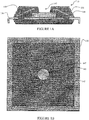
- the open cavity concept is used to expose a certain sensor area to the environment (for example, a specific top area of an integrated circuit die). It is important that, during the manufacturing process, the sensor area is not scratched, punctured, nor covered with any resin residue from the mold operation. According to various embodiments, all those issues are resolved, and the sensor device can be economically produced.
- a cavity or hole is created in a plastic package such that there will be no resin bleed from mold flash nor can there be any damage to the sensor area.
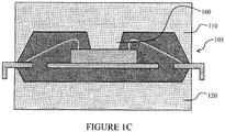
- a retractable spring-loaded pin or pins are used within the mold to create the cavity (for example, in a top half of a mold). The spring-loaded pins actually retracts back when the mold is closed and thus protect the sensor area on the silicon die from being covered by mold compound.
- One aspect of the invention provides a method for manufacturing open cavity integrated circuit packages, the method comprising: placing a wire-bound integrated circuit in a mold; forcing a pin to contact a die of the wire-bound integrated circuit by applying a force between the pin and the mold; injecting plastic into the mold; allowing the plastic to set around the integrated circuit to form a package having an open cavity defined by the pin; and removing the open cavity integrated circuit package from the mold.
- a mold for forming a package for an integrated circuit sensor device comprising: a bottom part for supporting an integrated circuit die; and a top part that is operable to be placed on top of said bottom part to form a cavity into which a plastic material can be injected to form the package, wherein the top part of the mold comprises a spring loaded pin arrangement comprising a cover that covers a sensor area on the integrated circuit die and provides for an opening when the plastic material is injected.
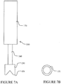
- the spring-loaded pin arrangement may comprise a spring housing supporting a pin that can be vertically moved against a spring force.
- the mold may further comprise a cover attached to said spring loaded pin configured to cover the sensor area.
- the cover may provide for a conical recess.
- the cover is made from high temperature plastic material.
- the pin can extend about 4 to 5 mm from the spring housing.
- the spring may provide for a spring force of about 80-120g.
- Still another aspect of the invention provides a process of manufacturing a sensor device comprising: placing an integrated circuit die on a support placed on a bottom part of a mold; wire-bonding the integrated circuit die; placing a top part of a mold on top of said bottom part to form a cavity for a package, wherein the top part of the mold comprises a spring-loaded pin arrangement comprising a cover that covers a sensor area on the integrated circuit die; and injecting plastic material into the mold formed by the top and bottom part, wherein the cover provides for an opening in the package formed by said injected plastic material.
- the placing a top part of a mold on top of said bottom part to form a cavity for a package comprises applying a force to the integrated circuit die independent of the closure force of the top part of the mold.
- a process of manufacturing an open cavity integrated circuit package may comprise: placing a wire-bound integrated circuit in a mold; forcing a pin to contact a die of the wire-bound integrated circuit by applying a force between the pin and the mold; injecting plastic into the mold; allowing the plastic to set around the integrated circuit to form a package having an open cavity defined by the pin; and removing the open cavity integrated circuit package from the mold.
- the forcing a pin to contact a die may comprise applying a spring force.
- the forcing a pin to contact a die may comprise applying a piston force.
- the forcing a pin to contact a die may comprise applying an elastic rod force.
- the forcing a pin to contact a die may comprise contacting the die with an annular contact face of the pin.
- the forcing a pin to contact a die may comprise forcing a plurality of pins to contact a die, and wherein the allowing the plastic to set comprises allowing the plastic to set around the plurality of pins to form a plurality of open cavities defined by the plurality of pins.
- the forcing a pin to contact a die comprises forcing a pin having a plurality of contact faces to contact a die, and wherein the allowing the plastic to set comprises allowing the plastic to set around the plurality of contact faces to form a plurality of open cavities defined by the plurality of contact faces.
- the process may further comprise pivoting the pin relative to the mold for uniform contact of a pin contact face with the die.
- the placing a wire-bound integrated circuit in a mold may comprise placing an array of wire-bound integrated circuits in a mold; wherein forcing a pin to contact a die comprises forcing a corresponding array of pins to contact the dies of the array of wire-bound integrated circuits; and wherein allowing the plastic to set comprises allowing the plastic to set around the array of integrated circuit to form an array of packages having open cavities defined by the array of pins.
- the placing a wire-bound integrated circuit in a mold may comprise closing the mold by applying a first force to the mold, wherein the forcing a pin to contact a die comprises applying a second force to the pin, wherein the first and second forces are different.
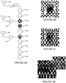
- a plurality of open cavities may be formed on a single IC.
- a plurality of covers 150 or pin heads 163 may be applied to a single IC during a molding sub-process. Where a plurality of pins are independently forced against the die, the independent application of force may ensure that the plastic encapsulant is unable to enter any of the open cavities because the plurality of pins are each able to make a firm contact with the die.
- a single cover 150 or pin head 163 may be applied to a single IC during a molding sub-process, but the single cover 150 or pin head 163 comprises a plurality of contact faces 151.
- the contact face 151 is annular, but in alternatively embodiments, the contact face may be any shape or configuration and may comprise a plurality of contact faces.
- a plurality of open cavities 147 may be useful where a plurality of sensors are attached to a single IC.
Landscapes
- Engineering & Computer Science (AREA)
- Microelectronics & Electronic Packaging (AREA)
- Manufacturing & Machinery (AREA)
- Mechanical Engineering (AREA)
- Health & Medical Sciences (AREA)
- General Health & Medical Sciences (AREA)
- Toxicology (AREA)
- Computer Hardware Design (AREA)
- Encapsulation Of And Coatings For Semiconductor Or Solid State Devices (AREA)
Claims (10)
- Form zum Ausbilden einer Verpackung für eine integrierter Schaltung einer Sensorvorrichtung, die aufweist
einen unteren Teil (120) zum Tragen eines integrierten Schaltungschips (140);
einen oberen Teil (110), der betätigbar ist, um auf dem unteren Teil (120) angeordnet zu werden, um einen Hohlraum auszubilden, in den ein Kunststoffmaterial eingespritzt werden kann, um die Verpackung auszubilden, wobei der obere Teil (110) der Form ein Federgehäuse (170) aus einer federgelagerten Stiftanordnung (190) aufweist, die weiterhin eine aus Hochtemperaturkunststoffmaterial hergestellte und eine Aussparung aufweisende zylindrische Abdeckung (150) aufweist, die ausgebildet ist, um einen Sensorbereich auf dem Chip der integrierten Schaltung abzudecken, und wobei der obere Teil (110) weiterhin eine Einspritzöffnung vorsieht, um das Einspritzen des Kunststoffmaterials zu ermöglichen, wobei sich ein Stift (160) von der zylindrischen Abdeckung (150) erstreckt und innerhalb des Federgehäuses (170) geführt ist, wobei der Stift (160) vertikal gegen eine Federkraft bewegt werden kann,
wobei der obere Teil (110) weiterhin eine Aussparung (180) aufweist, die sich von der Öffnung in Richtung des Hohlraums erstreckt und ausgebildet ist, um die zylindrische Abdeckung (150) aufzunehmen, wenn der obere Teil (110) auf dem unteren Teil (120) angeordnet ist,
wobei sich der Stift (160) 4 bis 5 mm vom Federgehäuse (170) erstrecken kann und wobei die Feder eine Federkraft von 80 bis 120 g bereitstellt. - Form gemäß Anspruch 1, wobei die zylindrische Abdeckung (150) eine ringförmige Kontaktfläche (151) und eine konische Aussparung aufweist.
- Form gemäß Anspruch 2, wobei ein Außendurchmesser der zylindrischen Abdeckung 1,2 mm breit ist.
- Form gemäß Anspruch 3, wobei der Innendurchmesser der zylindrischen Abdeckung (150) 1,0 mm beträgt.
- Form gemäß einem der vorhergehenden Ansprüche, die eine Vielzahl von federgelagerten Stiftanordnungen aufweist, die jeweils eine zylindrische Abdeckung (150) aufweisen, die einen Sensorbereich auf dem integrierten Schaltungschip (140) abdeckt.
- Verfahren zum Herstellen einer Verpackung für eine integrierter Schaltung mit offenem Hohlraum unter Verwendung einer Form gemäß einem der vorhergehenden Ansprüche, wobei das Verfahren aufweist:Platzieren einer drahtgebundenen integrierten Schaltung in der Form (110, 120);Erzwingen, dass die zylindrische Abdeckung (150) den Chip (140) der drahtgebundenen integrierten Schaltung kontaktiert, indem eine Kraft zwischen dem Stift (160) und der Form (110) aufgebracht wird;Einspritzen von Kunststoff in die Form (110, 120);Ermöglichen, dass der Kunststoff um die integrierte Schaltung aushärtet, um eine Verpackung auszubilden, die einen offenen Hohlraum aufweist, der durch die zylindrische Abdeckung (150) definiert ist; undEntfernen der integrierten Schaltung mit offenem Hohlraum aus der Form (110, 120).
- Verfahren zum Herstellen einer Verpackung für eine integrierter Schaltung mit offenem Hohlraum nach Anspruch 6, wobei das Erzwingen, dass ein Stift einen Chip kontaktiert, das Aufbringen einer Federkraft aufweist.
- Verfahren zum Herstellen einer Verpackung für eine integrierter Schaltung mit offenem Hohlraum gemäß einem der vorhergehenden Ansprüche 6 bis 7, wobei das Erzwingen, dass ein Stift einen Chip kontaktiert, das Erzwingen aufweist, dass eine Vielzahl von Stiften einen Chip kontaktiert und wobei das Ermöglichen, dass der Kunststoff aushärtet, das Ermöglichen aufweist, dass der Kunststoff um die Vielzahl von Stiften aushärtet, um eine Vielzahl von offenen Hohlräumen auszubilden, die durch die Vielzahl von Stiften definiert ist.
- Verfahren zum Herstellen einer Verpackung für eine integrierter Schaltung mit offenem Hohlraum gemäß einem der vorhergehenden Ansprüche 6 bis 8, das weiterhin zur gleichmäßigen Kontaktierung einer Kontaktfläche (151) einer zylindrischen Abdeckung mit dem Chip (140) das Schwenken des Stifts (160) relativ zur Form (110, 120) aufweist.
- Verfahren zum Herstellen einer Verpackung für eine integrierter Schaltung mit offenem Hohlraum gemäß einem der vorhergehenden Ansprüche 6 bis 9, wobei das Platzieren einer drahtgebundenen integrierten Schaltung in einer Form (110, 120) das Platzieren eines Arrays von drahtgebundenen integrierten Schaltungen in einer Form aufweist; wobei das Erzwingen einer zylindrischen Abdeckung (150) einen Chip (140) zu kontaktieren das Erzwingen eines entsprechenden Arrays von Stiften die Chips des Arrays von drahtgebundenen integrierten Schaltungen zu kontaktieren aufweist; und wobei das Ermöglichen des Aushärtens des Kunststoffs das Ermöglichen des Aushärtens des Kunststoffs um das Array der integrierten Schaltungen aufweist, um ein Array von Verpackungen auszubilden, die offene Hohlräume aufweisen, die durch das Array von Stiften definiert sind.
Applications Claiming Priority (3)
| Application Number | Priority Date | Filing Date | Title |
|---|---|---|---|
| US201361755889P | 2013-01-23 | 2013-01-23 | |
| US14/157,382 US9269597B2 (en) | 2013-01-23 | 2014-01-16 | Open cavity plastic package |
| PCT/US2014/012512 WO2014116677A1 (en) | 2013-01-23 | 2014-01-22 | Open cavity plastic package |
Publications (2)
| Publication Number | Publication Date |
|---|---|
| EP2948979A1 EP2948979A1 (de) | 2015-12-02 |
| EP2948979B1 true EP2948979B1 (de) | 2020-08-05 |
Family
ID=51208008
Family Applications (1)
| Application Number | Title | Priority Date | Filing Date |
|---|---|---|---|
| EP14702428.5A Active EP2948979B1 (de) | 2013-01-23 | 2014-01-22 | Kunststoffverpackung mit offenem hohlraum |
Country Status (6)
| Country | Link |
|---|---|
| US (2) | US9269597B2 (de) |
| EP (1) | EP2948979B1 (de) |
| KR (1) | KR20150111972A (de) |
| CN (1) | CN104969336B (de) |
| TW (1) | TWI604577B (de) |
| WO (1) | WO2014116677A1 (de) |
Families Citing this family (18)
| Publication number | Priority date | Publication date | Assignee | Title |
|---|---|---|---|---|
| JP5583487B2 (ja) * | 2010-06-14 | 2014-09-03 | 矢崎総業株式会社 | ヒューズユニット、型構造及び型構造を用いた成形方法 |
| US9269597B2 (en) | 2013-01-23 | 2016-02-23 | Microchip Technology Incorporated | Open cavity plastic package |
| ES2768272T3 (es) * | 2014-03-05 | 2020-06-22 | Yazaki Europe Ltd | Herramienta de moldeo |
| DE112014007140B4 (de) * | 2014-11-07 | 2024-05-02 | Mitsubishi Electric Corporation | Leistungshalbleiteranordnung und Verfahren zum Herstellen derselben |
| US9355870B1 (en) | 2015-01-15 | 2016-05-31 | Silicon Laboratories Inc. | Integrated circuit with sensor area and resin dam |
| US9431311B1 (en) | 2015-02-19 | 2016-08-30 | Semiconductor Components Industries, Llc | Semiconductor package with elastic coupler and related methods |
| JP6079925B1 (ja) * | 2016-03-30 | 2017-02-15 | 第一精工株式会社 | 樹脂封止装置及び樹脂封止装置の異常検知方法 |
| JP6319399B2 (ja) * | 2016-10-28 | 2018-05-09 | 株式会社デンソー | インサート成形用金型 |
| US10199356B2 (en) | 2017-02-24 | 2019-02-05 | Micron Technology, Inc. | Semiconductor device assembles with electrically functional heat transfer structures |
| US10090282B1 (en) * | 2017-06-13 | 2018-10-02 | Micron Technology, Inc. | Semiconductor device assemblies with lids including circuit elements |
| DE102017131110B4 (de) * | 2017-12-22 | 2025-01-02 | OSRAM Opto Semiconductors Gesellschaft mit beschränkter Haftung | Verfahren und formwerkzeug zum einbetten von optoelektronischen bauelementen in eine schicht |
| JP7331571B2 (ja) * | 2019-09-17 | 2023-08-23 | I-Pex株式会社 | 樹脂封止用金型及び樹脂封止方法 |
| DE102020201666A1 (de) * | 2020-02-11 | 2021-08-12 | Robert Bosch Gesellschaft mit beschränkter Haftung | Mold-Vorrichtung mit selbsttätig verstopfenden Einschusskanal |
| WO2022021094A1 (zh) * | 2020-07-28 | 2022-02-03 | 华为技术有限公司 | 一种功率模块及制备模具、设备 |
| US12309954B1 (en) | 2020-09-10 | 2025-05-20 | Verily Life Sciences Llc | Protective structures with integrated electrical interconnects for active implantable medical devices |
| US20220221353A1 (en) * | 2021-01-12 | 2022-07-14 | Texas Instruments Incorporated | Semiconductor force sensors |
| CN113451238B (zh) * | 2021-07-16 | 2022-06-21 | 贵州中芯微电子科技有限公司 | 一种中空式集成电路封装 |
| CN118486612B (zh) * | 2024-06-03 | 2025-10-14 | 安徽丰芯半导体有限公司 | 芯片封装的压模装置 |
Citations (3)
| Publication number | Priority date | Publication date | Assignee | Title |
|---|---|---|---|---|
| JPS5963735A (ja) * | 1982-10-05 | 1984-04-11 | Rohm Co Ltd | 半導体装置の製造方法 |
| JPH09304211A (ja) * | 1996-05-15 | 1997-11-28 | Omron Corp | 静電容量型圧力センサのパッケージング構造およびパッケージング方法 |
| WO2003028086A1 (en) * | 2001-09-26 | 2003-04-03 | European Semiconductor Assembly (Eurasem) B.V. | Method for encapsulating a chip and/or other article |
Family Cites Families (15)
| Publication number | Priority date | Publication date | Assignee | Title |
|---|---|---|---|---|
| US4452420A (en) * | 1982-09-30 | 1984-06-05 | Lynn Lundquist | Compensating core pin for plastic injection molds |
| JP2705361B2 (ja) | 1991-05-30 | 1998-01-28 | 三菱電機株式会社 | 中空型樹脂封止半導体圧力センサ製造用金型 |
| SE514116C2 (sv) * | 1994-10-19 | 2001-01-08 | Ericsson Telefon Ab L M | Förfarande för framställning av en kapslad optokomponent, gjutform för kapsling av en optokomponent och tryckanordning för gjutform |
| JP4024335B2 (ja) | 1996-01-26 | 2007-12-19 | ハリス コーポレイション | 集積回路のダイを露出させる開口部を有する集積回路装置とその製造方法 |
| US5997798A (en) * | 1997-06-27 | 1999-12-07 | International Business Machines Corporation | Biasing mold for integrated circuit chip assembly encapsulation |
| EP1220309A1 (de) | 2000-12-28 | 2002-07-03 | STMicroelectronics S.r.l. | Herstellungsverfahren einer elektronischen Packungsanordnung |
| US7304362B2 (en) | 2002-05-20 | 2007-12-04 | Stmicroelectronics, Inc. | Molded integrated circuit package with exposed active area |
| US7109574B2 (en) | 2002-07-26 | 2006-09-19 | Stmicroelectronics, Inc. | Integrated circuit package with exposed die surfaces and auxiliary attachment |
| JP4519424B2 (ja) * | 2003-06-26 | 2010-08-04 | ルネサスエレクトロニクス株式会社 | 樹脂モールド型半導体装置 |
| DE102005010311A1 (de) * | 2005-03-03 | 2006-09-14 | Atmel Germany Gmbh | Verfahren und Gießform zur Herstellung eines optischen Halbleitermoduls |
| JP2008066696A (ja) * | 2006-08-10 | 2008-03-21 | Denso Corp | 半導体製造装置および半導体製造方法 |
| DE102011004381A1 (de) | 2011-02-18 | 2012-08-23 | Robert Bosch Gmbh | Moldmodul mit Sensorelement |
| EP2573804A1 (de) | 2011-09-21 | 2013-03-27 | Nxp B.V. | Integrierte Schaltung mit Sensor und Verfahren zur Ihrer Herstellung |
| US8501517B1 (en) * | 2012-04-09 | 2013-08-06 | Freescale Semiconductor, Inc. | Method of assembling pressure sensor device |
| US9269597B2 (en) | 2013-01-23 | 2016-02-23 | Microchip Technology Incorporated | Open cavity plastic package |
-
2014
- 2014-01-16 US US14/157,382 patent/US9269597B2/en active Active
- 2014-01-22 CN CN201480005724.3A patent/CN104969336B/zh active Active
- 2014-01-22 KR KR1020157022855A patent/KR20150111972A/ko not_active Ceased
- 2014-01-22 EP EP14702428.5A patent/EP2948979B1/de active Active
- 2014-01-22 WO PCT/US2014/012512 patent/WO2014116677A1/en not_active Ceased
- 2014-01-23 TW TW103102595A patent/TWI604577B/zh active
-
2016
- 2016-02-22 US US15/050,438 patent/US9630352B2/en active Active
Patent Citations (3)
| Publication number | Priority date | Publication date | Assignee | Title |
|---|---|---|---|---|
| JPS5963735A (ja) * | 1982-10-05 | 1984-04-11 | Rohm Co Ltd | 半導体装置の製造方法 |
| JPH09304211A (ja) * | 1996-05-15 | 1997-11-28 | Omron Corp | 静電容量型圧力センサのパッケージング構造およびパッケージング方法 |
| WO2003028086A1 (en) * | 2001-09-26 | 2003-04-03 | European Semiconductor Assembly (Eurasem) B.V. | Method for encapsulating a chip and/or other article |
Also Published As
| Publication number | Publication date |
|---|---|
| EP2948979A1 (de) | 2015-12-02 |
| CN104969336A (zh) | 2015-10-07 |
| US9269597B2 (en) | 2016-02-23 |
| KR20150111972A (ko) | 2015-10-06 |
| CN104969336B (zh) | 2019-02-01 |
| TWI604577B (zh) | 2017-11-01 |
| US20160167273A1 (en) | 2016-06-16 |
| TW201438163A (zh) | 2014-10-01 |
| WO2014116677A1 (en) | 2014-07-31 |
| US20140206122A1 (en) | 2014-07-24 |
| US9630352B2 (en) | 2017-04-25 |
Similar Documents
| Publication | Publication Date | Title |
|---|---|---|
| US9630352B2 (en) | Open cavity plastic package | |
| EP1465244B1 (de) | Integrierte Schaltungsverpackung mit freiliegenden Chipoberflächen und Hilfsbefestigung | |
| KR970006531B1 (ko) | 전자 소자 패키지 및 제조방법 | |
| KR101031394B1 (ko) | 광 센서 패키지 | |
| EP3026696B1 (de) | Verpackung für auf mechanische und thermomechanische beanspruchung ansprechende halbleiterbauelemente wie etwa mems-drucksensoren | |
| US7582954B1 (en) | Optical leadless leadframe package | |
| US20140374848A1 (en) | Semiconductor sensor device with metal lid | |
| US20050279166A1 (en) | Semiconductor acceleration sensor device and method for manufacturing the same | |
| US20090314095A1 (en) | Pressure sensing device package and manufacturing method thereof | |
| US5378656A (en) | Leadframe, semiconductor integrated circuit device using the same, and method of and process for fabricating the same | |
| US20050184404A1 (en) | Photosensitive semiconductor package with support member and method for fabricating the same | |
| US20130119538A1 (en) | Wafer level chip size package | |
| JP6598642B2 (ja) | 樹脂封止装置及び樹脂封止方法 | |
| US6291263B1 (en) | Method of fabricating an integrated circuit package having a core-hollowed encapsulation body | |
| CN100495689C (zh) | 包装光学传感器的方法和图像传感器装置 | |
| US20050082490A1 (en) | Optical semiconductor housing with transparent chip and method for making same | |
| US20150035130A1 (en) | Integrated Circuit with Stress Isolation | |
| US8237293B2 (en) | Semiconductor package with protective tape | |
| KR20160081289A (ko) | 반도체 패키지 제조용 보트 및 반도체 패키지 제조 방법 | |
| JP2000176967A (ja) | 樹脂封止装置 | |
| US9368424B2 (en) | Method of fabricating a semiconductor device used in a stacked-type semiconductor device | |
| KR20090066517A (ko) | 웨이퍼 레벨 반도체 패키지 및 그 제조 방법 | |
| TWI837600B (zh) | 封裝結構及其製作設備 | |
| JP2011014606A (ja) | 半導体装置の製造方法 | |
| CN115881684A (zh) | 用于芯片封装的条带、封装模块及智能卡 |
Legal Events
| Date | Code | Title | Description |
|---|---|---|---|
| PUAI | Public reference made under article 153(3) epc to a published international application that has entered the european phase |
Free format text: ORIGINAL CODE: 0009012 |
|
| 17P | Request for examination filed |
Effective date: 20150820 |
|
| AK | Designated contracting states |
Kind code of ref document: A1 Designated state(s): AL AT BE BG CH CY CZ DE DK EE ES FI FR GB GR HR HU IE IS IT LI LT LU LV MC MK MT NL NO PL PT RO RS SE SI SK SM TR |
|
| AX | Request for extension of the european patent |
Extension state: BA ME |
|
| DAX | Request for extension of the european patent (deleted) | ||
| STAA | Information on the status of an ep patent application or granted ep patent |
Free format text: STATUS: EXAMINATION IS IN PROGRESS |
|
| 17Q | First examination report despatched |
Effective date: 20161129 |
|
| GRAP | Despatch of communication of intention to grant a patent |
Free format text: ORIGINAL CODE: EPIDOSNIGR1 |
|
| STAA | Information on the status of an ep patent application or granted ep patent |
Free format text: STATUS: GRANT OF PATENT IS INTENDED |
|
| INTG | Intention to grant announced |
Effective date: 20200224 |
|
| GRAS | Grant fee paid |
Free format text: ORIGINAL CODE: EPIDOSNIGR3 |
|
| GRAA | (expected) grant |
Free format text: ORIGINAL CODE: 0009210 |
|
| STAA | Information on the status of an ep patent application or granted ep patent |
Free format text: STATUS: THE PATENT HAS BEEN GRANTED |
|
| AK | Designated contracting states |
Kind code of ref document: B1 Designated state(s): AL AT BE BG CH CY CZ DE DK EE ES FI FR GB GR HR HU IE IS IT LI LT LU LV MC MK MT NL NO PL PT RO RS SE SI SK SM TR |
|
| REG | Reference to a national code |
Ref country code: GB Ref legal event code: FG4D |
|
| REG | Reference to a national code |
Ref country code: CH Ref legal event code: EP |
|
| REG | Reference to a national code |
Ref country code: AT Ref legal event code: REF Ref document number: 1299909 Country of ref document: AT Kind code of ref document: T Effective date: 20200815 |
|
| REG | Reference to a national code |
Ref country code: DE Ref legal event code: R096 Ref document number: 602014068525 Country of ref document: DE |
|
| REG | Reference to a national code |
Ref country code: IE Ref legal event code: FG4D |
|
| REG | Reference to a national code |
Ref country code: LT Ref legal event code: MG4D |
|
| REG | Reference to a national code |
Ref country code: NL Ref legal event code: MP Effective date: 20200805 |
|
| REG | Reference to a national code |
Ref country code: AT Ref legal event code: MK05 Ref document number: 1299909 Country of ref document: AT Kind code of ref document: T Effective date: 20200805 |
|
| PG25 | Lapsed in a contracting state [announced via postgrant information from national office to epo] |
Ref country code: LT Free format text: LAPSE BECAUSE OF FAILURE TO SUBMIT A TRANSLATION OF THE DESCRIPTION OR TO PAY THE FEE WITHIN THE PRESCRIBED TIME-LIMIT Effective date: 20200805 Ref country code: ES Free format text: LAPSE BECAUSE OF FAILURE TO SUBMIT A TRANSLATION OF THE DESCRIPTION OR TO PAY THE FEE WITHIN THE PRESCRIBED TIME-LIMIT Effective date: 20200805 Ref country code: BG Free format text: LAPSE BECAUSE OF FAILURE TO SUBMIT A TRANSLATION OF THE DESCRIPTION OR TO PAY THE FEE WITHIN THE PRESCRIBED TIME-LIMIT Effective date: 20201105 Ref country code: HR Free format text: LAPSE BECAUSE OF FAILURE TO SUBMIT A TRANSLATION OF THE DESCRIPTION OR TO PAY THE FEE WITHIN THE PRESCRIBED TIME-LIMIT Effective date: 20200805 Ref country code: NO Free format text: LAPSE BECAUSE OF FAILURE TO SUBMIT A TRANSLATION OF THE DESCRIPTION OR TO PAY THE FEE WITHIN THE PRESCRIBED TIME-LIMIT Effective date: 20201105 Ref country code: PT Free format text: LAPSE BECAUSE OF FAILURE TO SUBMIT A TRANSLATION OF THE DESCRIPTION OR TO PAY THE FEE WITHIN THE PRESCRIBED TIME-LIMIT Effective date: 20201207 Ref country code: FI Free format text: LAPSE BECAUSE OF FAILURE TO SUBMIT A TRANSLATION OF THE DESCRIPTION OR TO PAY THE FEE WITHIN THE PRESCRIBED TIME-LIMIT Effective date: 20200805 Ref country code: GR Free format text: LAPSE BECAUSE OF FAILURE TO SUBMIT A TRANSLATION OF THE DESCRIPTION OR TO PAY THE FEE WITHIN THE PRESCRIBED TIME-LIMIT Effective date: 20201106 Ref country code: SE Free format text: LAPSE BECAUSE OF FAILURE TO SUBMIT A TRANSLATION OF THE DESCRIPTION OR TO PAY THE FEE WITHIN THE PRESCRIBED TIME-LIMIT Effective date: 20200805 Ref country code: AT Free format text: LAPSE BECAUSE OF FAILURE TO SUBMIT A TRANSLATION OF THE DESCRIPTION OR TO PAY THE FEE WITHIN THE PRESCRIBED TIME-LIMIT Effective date: 20200805 |
|
| PG25 | Lapsed in a contracting state [announced via postgrant information from national office to epo] |
Ref country code: IS Free format text: LAPSE BECAUSE OF FAILURE TO SUBMIT A TRANSLATION OF THE DESCRIPTION OR TO PAY THE FEE WITHIN THE PRESCRIBED TIME-LIMIT Effective date: 20201205 Ref country code: RS Free format text: LAPSE BECAUSE OF FAILURE TO SUBMIT A TRANSLATION OF THE DESCRIPTION OR TO PAY THE FEE WITHIN THE PRESCRIBED TIME-LIMIT Effective date: 20200805 Ref country code: PL Free format text: LAPSE BECAUSE OF FAILURE TO SUBMIT A TRANSLATION OF THE DESCRIPTION OR TO PAY THE FEE WITHIN THE PRESCRIBED TIME-LIMIT Effective date: 20200805 Ref country code: LV Free format text: LAPSE BECAUSE OF FAILURE TO SUBMIT A TRANSLATION OF THE DESCRIPTION OR TO PAY THE FEE WITHIN THE PRESCRIBED TIME-LIMIT Effective date: 20200805 Ref country code: NL Free format text: LAPSE BECAUSE OF FAILURE TO SUBMIT A TRANSLATION OF THE DESCRIPTION OR TO PAY THE FEE WITHIN THE PRESCRIBED TIME-LIMIT Effective date: 20200805 |
|
| PG25 | Lapsed in a contracting state [announced via postgrant information from national office to epo] |
Ref country code: RO Free format text: LAPSE BECAUSE OF FAILURE TO SUBMIT A TRANSLATION OF THE DESCRIPTION OR TO PAY THE FEE WITHIN THE PRESCRIBED TIME-LIMIT Effective date: 20200805 Ref country code: SM Free format text: LAPSE BECAUSE OF FAILURE TO SUBMIT A TRANSLATION OF THE DESCRIPTION OR TO PAY THE FEE WITHIN THE PRESCRIBED TIME-LIMIT Effective date: 20200805 Ref country code: CZ Free format text: LAPSE BECAUSE OF FAILURE TO SUBMIT A TRANSLATION OF THE DESCRIPTION OR TO PAY THE FEE WITHIN THE PRESCRIBED TIME-LIMIT Effective date: 20200805 Ref country code: DK Free format text: LAPSE BECAUSE OF FAILURE TO SUBMIT A TRANSLATION OF THE DESCRIPTION OR TO PAY THE FEE WITHIN THE PRESCRIBED TIME-LIMIT Effective date: 20200805 Ref country code: EE Free format text: LAPSE BECAUSE OF FAILURE TO SUBMIT A TRANSLATION OF THE DESCRIPTION OR TO PAY THE FEE WITHIN THE PRESCRIBED TIME-LIMIT Effective date: 20200805 |
|
| REG | Reference to a national code |
Ref country code: DE Ref legal event code: R097 Ref document number: 602014068525 Country of ref document: DE |
|
| PG25 | Lapsed in a contracting state [announced via postgrant information from national office to epo] |
Ref country code: AL Free format text: LAPSE BECAUSE OF FAILURE TO SUBMIT A TRANSLATION OF THE DESCRIPTION OR TO PAY THE FEE WITHIN THE PRESCRIBED TIME-LIMIT Effective date: 20200805 |
|
| PLBE | No opposition filed within time limit |
Free format text: ORIGINAL CODE: 0009261 |
|
| STAA | Information on the status of an ep patent application or granted ep patent |
Free format text: STATUS: NO OPPOSITION FILED WITHIN TIME LIMIT |
|
| PG25 | Lapsed in a contracting state [announced via postgrant information from national office to epo] |
Ref country code: SK Free format text: LAPSE BECAUSE OF FAILURE TO SUBMIT A TRANSLATION OF THE DESCRIPTION OR TO PAY THE FEE WITHIN THE PRESCRIBED TIME-LIMIT Effective date: 20200805 |
|
| 26N | No opposition filed |
Effective date: 20210507 |
|
| PG25 | Lapsed in a contracting state [announced via postgrant information from national office to epo] |
Ref country code: IT Free format text: LAPSE BECAUSE OF FAILURE TO SUBMIT A TRANSLATION OF THE DESCRIPTION OR TO PAY THE FEE WITHIN THE PRESCRIBED TIME-LIMIT Effective date: 20200805 |
|
| PG25 | Lapsed in a contracting state [announced via postgrant information from national office to epo] |
Ref country code: SI Free format text: LAPSE BECAUSE OF FAILURE TO SUBMIT A TRANSLATION OF THE DESCRIPTION OR TO PAY THE FEE WITHIN THE PRESCRIBED TIME-LIMIT Effective date: 20200805 Ref country code: MC Free format text: LAPSE BECAUSE OF FAILURE TO SUBMIT A TRANSLATION OF THE DESCRIPTION OR TO PAY THE FEE WITHIN THE PRESCRIBED TIME-LIMIT Effective date: 20200805 |
|
| REG | Reference to a national code |
Ref country code: CH Ref legal event code: PL |
|
| GBPC | Gb: european patent ceased through non-payment of renewal fee |
Effective date: 20210122 |
|
| PG25 | Lapsed in a contracting state [announced via postgrant information from national office to epo] |
Ref country code: LU Free format text: LAPSE BECAUSE OF NON-PAYMENT OF DUE FEES Effective date: 20210122 |
|
| REG | Reference to a national code |
Ref country code: BE Ref legal event code: MM Effective date: 20210131 |
|
| PG25 | Lapsed in a contracting state [announced via postgrant information from national office to epo] |
Ref country code: FR Free format text: LAPSE BECAUSE OF NON-PAYMENT OF DUE FEES Effective date: 20210131 |
|
| PG25 | Lapsed in a contracting state [announced via postgrant information from national office to epo] |
Ref country code: LI Free format text: LAPSE BECAUSE OF NON-PAYMENT OF DUE FEES Effective date: 20210131 Ref country code: GB Free format text: LAPSE BECAUSE OF NON-PAYMENT OF DUE FEES Effective date: 20210122 Ref country code: CH Free format text: LAPSE BECAUSE OF NON-PAYMENT OF DUE FEES Effective date: 20210131 |
|
| PG25 | Lapsed in a contracting state [announced via postgrant information from national office to epo] |
Ref country code: IE Free format text: LAPSE BECAUSE OF NON-PAYMENT OF DUE FEES Effective date: 20210122 |
|
| PG25 | Lapsed in a contracting state [announced via postgrant information from national office to epo] |
Ref country code: IS Free format text: LAPSE BECAUSE OF FAILURE TO SUBMIT A TRANSLATION OF THE DESCRIPTION OR TO PAY THE FEE WITHIN THE PRESCRIBED TIME-LIMIT Effective date: 20201205 |
|
| PG25 | Lapsed in a contracting state [announced via postgrant information from national office to epo] |
Ref country code: BE Free format text: LAPSE BECAUSE OF NON-PAYMENT OF DUE FEES Effective date: 20210131 |
|
| PG25 | Lapsed in a contracting state [announced via postgrant information from national office to epo] |
Ref country code: HU Free format text: LAPSE BECAUSE OF FAILURE TO SUBMIT A TRANSLATION OF THE DESCRIPTION OR TO PAY THE FEE WITHIN THE PRESCRIBED TIME-LIMIT; INVALID AB INITIO Effective date: 20140122 |
|
| PG25 | Lapsed in a contracting state [announced via postgrant information from national office to epo] |
Ref country code: CY Free format text: LAPSE BECAUSE OF FAILURE TO SUBMIT A TRANSLATION OF THE DESCRIPTION OR TO PAY THE FEE WITHIN THE PRESCRIBED TIME-LIMIT Effective date: 20200805 |
|
| P01 | Opt-out of the competence of the unified patent court (upc) registered |
Effective date: 20230528 |
|
| PG25 | Lapsed in a contracting state [announced via postgrant information from national office to epo] |
Ref country code: MK Free format text: LAPSE BECAUSE OF FAILURE TO SUBMIT A TRANSLATION OF THE DESCRIPTION OR TO PAY THE FEE WITHIN THE PRESCRIBED TIME-LIMIT Effective date: 20200805 |
|
| PG25 | Lapsed in a contracting state [announced via postgrant information from national office to epo] |
Ref country code: MT Free format text: LAPSE BECAUSE OF FAILURE TO SUBMIT A TRANSLATION OF THE DESCRIPTION OR TO PAY THE FEE WITHIN THE PRESCRIBED TIME-LIMIT Effective date: 20200805 |
|
| REG | Reference to a national code |
Ref country code: DE Ref legal event code: R079 Ref document number: 602014068525 Country of ref document: DE Free format text: PREVIOUS MAIN CLASS: H01L0021560000 Ipc: H10W0074010000 |
|
| PG25 | Lapsed in a contracting state [announced via postgrant information from national office to epo] |
Ref country code: TR Free format text: LAPSE BECAUSE OF FAILURE TO SUBMIT A TRANSLATION OF THE DESCRIPTION OR TO PAY THE FEE WITHIN THE PRESCRIBED TIME-LIMIT Effective date: 20200805 |
|
| PGFP | Annual fee paid to national office [announced via postgrant information from national office to epo] |
Ref country code: DE Payment date: 20251217 Year of fee payment: 13 |