EP2940699A1 - Oxide superconductor wire - Google Patents
Oxide superconductor wire Download PDFInfo
- Publication number
- EP2940699A1 EP2940699A1 EP13868560.7A EP13868560A EP2940699A1 EP 2940699 A1 EP2940699 A1 EP 2940699A1 EP 13868560 A EP13868560 A EP 13868560A EP 2940699 A1 EP2940699 A1 EP 2940699A1
- Authority
- EP
- European Patent Office
- Prior art keywords
- layer
- oxide superconductor
- thickness
- superconductor
- laminate
- Prior art date
- Legal status (The legal status is an assumption and is not a legal conclusion. Google has not performed a legal analysis and makes no representation as to the accuracy of the status listed.)
- Granted
Links
Images


Classifications
-
- C—CHEMISTRY; METALLURGY
- C01—INORGANIC CHEMISTRY
- C01G—COMPOUNDS CONTAINING METALS NOT COVERED BY SUBCLASSES C01D OR C01F
- C01G1/00—Methods of preparing compounds of metals not covered by subclasses C01B, C01C, C01D, or C01F, in general
-
- H—ELECTRICITY
- H01—ELECTRIC ELEMENTS
- H01B—CABLES; CONDUCTORS; INSULATORS; SELECTION OF MATERIALS FOR THEIR CONDUCTIVE, INSULATING OR DIELECTRIC PROPERTIES
- H01B12/00—Superconductive or hyperconductive conductors, cables, or transmission lines
- H01B12/02—Superconductive or hyperconductive conductors, cables, or transmission lines characterised by their form
- H01B12/06—Films or wires on bases or cores
-
- H—ELECTRICITY
- H01—ELECTRIC ELEMENTS
- H01F—MAGNETS; INDUCTANCES; TRANSFORMERS; SELECTION OF MATERIALS FOR THEIR MAGNETIC PROPERTIES
- H01F6/00—Superconducting magnets; Superconducting coils
- H01F6/06—Coils, e.g. winding, insulating, terminating or casing arrangements therefor
-
- H—ELECTRICITY
- H10—SEMICONDUCTOR DEVICES; ELECTRIC SOLID-STATE DEVICES NOT OTHERWISE PROVIDED FOR
- H10N—ELECTRIC SOLID-STATE DEVICES NOT OTHERWISE PROVIDED FOR
- H10N60/00—Superconducting devices
- H10N60/01—Manufacture or treatment
- H10N60/0268—Manufacture or treatment of devices comprising copper oxide
- H10N60/0801—Manufacture or treatment of filaments or composite wires
-
- H—ELECTRICITY
- H10—SEMICONDUCTOR DEVICES; ELECTRIC SOLID-STATE DEVICES NOT OTHERWISE PROVIDED FOR
- H10N—ELECTRIC SOLID-STATE DEVICES NOT OTHERWISE PROVIDED FOR
- H10N60/00—Superconducting devices
- H10N60/20—Permanent superconducting devices
- H10N60/203—Permanent superconducting devices comprising high-Tc ceramic materials
-
- H—ELECTRICITY
- H10—SEMICONDUCTOR DEVICES; ELECTRIC SOLID-STATE DEVICES NOT OTHERWISE PROVIDED FOR
- H10N—ELECTRIC SOLID-STATE DEVICES NOT OTHERWISE PROVIDED FOR
- H10N60/00—Superconducting devices
- H10N60/30—Devices switchable between superconducting and normal states
-
- H—ELECTRICITY
- H10—SEMICONDUCTOR DEVICES; ELECTRIC SOLID-STATE DEVICES NOT OTHERWISE PROVIDED FOR
- H10N—ELECTRIC SOLID-STATE DEVICES NOT OTHERWISE PROVIDED FOR
- H10N60/00—Superconducting devices
- H10N60/80—Constructional details
- H10N60/85—Superconducting active materials
- H10N60/855—Ceramic superconductors
Definitions
- the present invention relates to an oxide superconductor wire used for superconductor equipment such as a superconductor current-limiting device.
- Electric equipment capable of solving the recent energy challenges includes superconductor equipment such as cable, coil, motor, magnet, and superconductor current-limiting device with the use of an oxide superconductor which is a low-loss electrically conductive material.
- an oxide superconductor such as an RE-123-based oxide superconductor (REBa 2 Cu 3 O 7-x : RE being a rare-earth element containing Y, Gd etc.) is known.
- the oxide superconductor exhibits superconductive properties at around the liquid nitrogen temperatures and is capable of maintaining a relatively high critical current density even in a strong magnetic field, and therefore is regarded as an extremely promising electrically conductive material in practice.
- Patent Document 1 discloses an oxide superconductor wire using a laminate which includes an oxide superconductor layer formed on a tape-shaped metal substrate via an interlayer having good crystal orientation and a protection layer formed so as to cover the oxide superconductor layer.
- the outer periphery of the laminate is provided with a stabilization layer formed by covering the outer periphery with a wide-width metal tape via a solder layer. Since the protection layer and the stabilization layer of such an oxide superconductor wire serve to bypass overcurrent in case of emergency, they are formed of low electrical resistance materials.
- the protection layer may be formed of Ag or an Ag alloy and the stabilization layer may be formed of Cu.
- Patent Document 2 describes the use of metals, as the high-resistance layer formed on the substrate or the oxide superconductor layer, of which the electrical resistivity is no less than 1 ⁇ 10 -7 ⁇ m and no more than 1 ⁇ 10 -5 ⁇ m at room temperature.
- the protection layer is formed of Ag or an Ag alloy and exhibits significantly lower volume resistivity compared to the stabilization layer. As the thickness of the protection layer is reduced, the thickness of the stabilization layer needs to be considerably thicker to compensate that, which will enlarge the thickness of the oxide superconductor wire. If the thickness of the oxide superconductor wire is enlarged, it will be impossible to increase the magnetic field density of the coil formed by winding the oxide superconductor wire.
- the present invention was made in view of the above-described circumstances and the object thereof is providing an oxide superconductor wire for use in superconductor current-limiting devices, which is, even if the thickness of the protection layer is reduced, capable of preventing burnout, exhibiting stable current limiting characteristics, and limiting the enlargement of the thickness of the oxide superconductor wire.
- An oxide superconductor wire includes: an oxide superconductor laminate including: a tape-shaped substrate, an interlayer laminated on the substrate, an oxide superconductor layer laminated on the interlayer, and a protection layer which is formed of Ag or an Ag alloy and laminated on the oxide superconductor layer; and a stabilization layer which is formed of a metal tape and formed on the protection layer of the superconductor laminate via a low melting point metal layer, wherein the thickness of the protection layer is 5 ⁇ m or less, and wherein a volume resistivity of the stabilization layer at room temperature is no less than 3.8 ⁇ cm and no more than 15 ⁇ cm.
- the thickness of the protection layer formed of Ag or an Ag alloy is 5 ⁇ m or less, it is possible to reduce the amount of Ag used for the oxide superconductor wire, and thereby reduce the cost.
- the volume resistivity of the metal tape at room temperature is no less than 3.8 ⁇ cm and no more than 15 ⁇ cm, it is possible, even when electric current 1.5-3 times the critical current is applied, to limit the excessive current and thereby prevent burnout of the oxide superconductor wire and achieve stable current limiting characteristics in superconductor current-limiting devices using the oxide superconductor wire even with the thickness of the protection layer of 5 ⁇ m or less.
- an oxide superconductor wire includes: a tape-shaped substrate, an interlayer laminated on the substrate, an oxide superconductor layer laminated on the interlayer, and a protection layer which is formed of Ag or an Ag alloy and laminated on the oxide superconductor layer; and a stabilization layer which is formed of a metal tape and formed on the protection layer of the superconductor laminate via a low melting point metal layer, wherein the thickness of the protection layer is 5 ⁇ m or less, and wherein a resistance value of the oxide superconductor wire per 1 cm width and 1 cm length at room temperature is no less than 150 ⁇ and no more than 100 m ⁇ .
- the thickness of the protection layer formed of Ag or an Ag alloy is 5 ⁇ m or less, it is possible to reduce the amount of Ag used for the oxide superconductor wire, and thereby to reduce the cost.
- the resistance value of the oxide superconductor wire per 1 cm width and 1 cm length at room temperature is no less than 150 ⁇ and no more than 100 m ⁇ , it is possible, even when electric current 1.5-3 times the critical current is applied, to limit the excessive current and thereby prevent the burnout of the oxide superconductor wire and achieve stable current limiting characteristics in superconductor current-limiting devices using the oxide superconductor wire even with the thickness of the protection layer of 5 ⁇ m or less.
- a width of the metal tape constituting the stabilization layer is greater than the width of the oxide superconductor laminate, and a top face of the protection layer of the oxide superconductor laminate, side faces of the protection layer, the oxide superconductor layer, the interlayer and the substrate, and at least a part of a back face of the substrate are covered with the stabilization layer via the low melting point metal layer.
- the thickness of the stabilization layer is no less than 9 ⁇ m and no more than 60 ⁇ m.
- the thickness of the stabilization layer is no less than 9 ⁇ m and no more than 60 ⁇ m. More specifically, the thickness of the metal tape covering the oxide superconductor laminate is no less than 9 ⁇ m and no more than 60 ⁇ m. With the metal tape having a thickness of no less than 9 ⁇ m, it is possible to prevent the metal tape from tearing in the process of covering the oxide superconductor laminate with the metal tape. Moreover, the metal tape having a thickness of 60 ⁇ m or less will facilitate the forming of the metal tape and reliably cover the oxide superconductor laminate.
- a superconductor coil according to the third aspect of the present invention includes the oxide superconductor wire described above.
- a superconductor current-limiting device includes the oxide superconductor wire described above.
- a superconductor equipment according to the fifth aspect of the present invention includes the oxide superconductor wire described above.
- the oxide superconductor wire in superconductor coils, superconductor current-limiting devices, and the other superconductor equipment, it is possible to enhance the protection performance of the superconductor equipment with respect to moisture. In addition, it is possible to prevent the burnout of the oxide superconductor wire when excessive current flows in the oxide superconductor wire. Accordingly, it is possible to achieve more reliable superconductor equipment compared to the conventional one.
- the thickness of the protection layer formed of Ag or an Ag alloy is 5 ⁇ m or less, it is possible to reduce the amount of Ag used for the oxide superconductor wire, and thereby reduce the cost.
- the volume resistivity of the metal tape at room temperature is no less than 3.8 ⁇ cm and no more than 15 ⁇ cm, it is possible, even when electric current 1.5-3 times the critical current is applied, to limit the excessive current, and thereby prevent burnout of the oxide superconductor wire and achieve stable current limiting characteristics in superconductor current-limiting devices using the oxide superconductor wire even with the thickness of the protection layer of 5 ⁇ m or less.
- oxide superconductor wires according to embodiments of the present invention will be described with reference to the drawings. It should be noted that, in the drawings, some parts are magnified in shape for the purpose of explanation, but the proportions, for example, of the components shown in the drawings are not necessarily the same as the actual ones.
- FIG. 1 is a perspective view showing a lateral cross section of the oxide superconductor wire according to an embodiment of the present invention.
- An oxide superconductor wire A according to the embodiment includes a tape-shaped oxide superconductor laminate 1 and a metal tape 2 formed of an electrically conductive material such as a copper and covering the oxide superconductor laminate 1.
- the oxide superconductor laminate 1 includes a tape-shaped substrate 3, an interlayer 4, an oxide superconductor layer 5, and a protection layer 6 as shown in FIG. 2 .
- the interlayer 4, the oxide superconductor layer 5, and the protection layer 6 are laminated onto the substrate 3 in this order.
- the substrate 3 may be one which is capable of being used for a substrate of common oxide superconductor wires and preferably has flexibility and elongated tape shape.
- the material of the substrate 3 preferably contains a metal which has high mechanical strength and heat resistance and can be easily processed into wires. Examples of such materials includes, for example, various kinds of heat-resistance metal materials including a nickel alloy such as stainless steel and HASTELLOY, and materials having ceramics arranged on the various kinds of metal materials.
- HASTELLOY (Trade name, HAYNES INT. INC., USA) is preferable among commercially available products.
- HASTELLOY such as HASTELLOY B, C, G, N, and W are available, which contain different amount of ingredients such as molybdenum, chromium, iron, and cobalt.
- Any of the HASTELLOYs can be used for the substrate 3.
- an oriented Ni-W alloy tape substrate may be employed, the substrate being formed by introducing texture into a nickel alloy.
- the thickness of the substrate 3 may be adjusted in accordance with the purpose, typically be 10 to 500 ⁇ m, and preferably be 20 to 200 ⁇ m.
- An example of the interlayer 4 may have a configuration in which a diffusion prevention layer, a bed layer, an orientation layer, and a cap layer are laminated in this order.
- the diffusion prevention layer will serve to prevent part of the constituent elements of the substrate 3 from diffusing and being admixed, as impurities, into the oxide superconductor layer 5, when heat treatment is performed to the layers formed above the diffusion prevention layer and, as a result, imparts thermal hysteresis to the substrate 3 and the other layers.
- the specific structure of the diffusion prevention layer is not particularly limited provided it is capable of providing the above-described effects. It is preferable to employ a diffusion prevention layer having a single-layer or multilayer structure constituted by Al 2 O 3 , Si 3 N 4 , GZO (Gd 2 Zr 2 O 7 ), or the like, which are relatively effective in preventing the admixture of impurities.
- the bed layer is used to prevent reactions of the constituent element at the interface between the substrate 3 and the oxide superconductor layer 5 and improve the orientation of layers which are provided on the bed layer.
- the specific structure of the bed layer is not particularly limited provided it is capable of providing the above-described effects. It is preferable to employ a bed layer having single-layer or multilayer structure constituted by a rare earth oxide which have high heat resistance, such as Y 2 O 3 , CeO 2 , La 2 O 3 , Dy 2 O 3 , Er 2 O 3 , Eu 2 O 3 , and Ho 2 O 3 .
- the orientation layer serves to control the crystal orientation of the cap layer and the oxide superconductor layer 5 which are formed thereon, prevent the constituent elements of the substrate 3 from diffusing into the oxide superconductor layer 5, and mitigate the difference between the substrate 3 and the oxide superconductor layer 5 in terms of physical characteristics such as coefficient of thermal expansion and lattice constant.
- the material of the orientation layer is not particularly limited provided it is capable of providing the above-described effects, but is preferably a metal oxide such as Gd 2 Zr 2 O 7 , MgO, ZrO 2 -Y 2 O 3 (YSZ), and the like.
- a layer having high crystal orientation can be obtained with an ion beam assisted deposition method (hereinafter, may be referred to as IBAD method) which is described later, which will further improve the crystal orientation of the cap layer and the oxide superconductor layer 5.
- IBAD method ion beam assisted deposition method
- the cap layer serves to strongly control the crystal orientation of the oxide superconductor layer 5 equally or more than the orientation layer, prevent the constituent elements of the oxide superconductor layer 5 from diffusing into the interlayer 4, and prevent reactions between the interlayer 4 and gases used in the process of laminating the oxide superconductor layer 5.
- the material of the cap layer is not particularly limited provided it is capable of providing above-described effects, but is preferably a metal oxide such as CeO 2 , LaMnO 3 , Y 2 O 3 , Al 2 O 3 , Gd 2 O 3 , ZrO 2 , Ho 2 O 3 , Nd 2 O 3 , and Zr 2 O 3 , in view of lattice matching with respect to the oxide superconductor layer 5.
- CeO 2 and LaMnO 3 are particularly preferable in view of the matching with respect to the oxide superconductor layer 5.
- the cap layer may include a Ce-M-O based oxide in which part of Ce atoms are substituted with the other metal atoms or metal ions.
- the oxide superconductor layer 5 serves to conduct an electric current when it is in a superconducting state.
- oxide superconductor materials having commonly-known compositions may be employed as the material of the oxide superconductor layer 5.
- examples thereof include a copper oxide superconductor such as RE-123 based superconductor and Bi based superconductor.
- the composition of the RE-123 based superconductor include REBa 2 Cu 3 O (7-x) (RE represents a rare-earth element such as Y, La, Nd, Sm, Er, and Gd while x represents deficient oxygen), more particularly Y123 (YBa 2 Cu 3 O (7-x) ) and Gd123 (GdBa 2 Cu 3 O (7-x) ).
- composition of the Bi based superconductor examples include Bi 2 Sr 2 Ca n-1 Cu n O 4+2n+ ⁇ (n represents the number of CuO 2 layers while ⁇ represents excess oxygen).
- n represents the number of CuO 2 layers while ⁇ represents excess oxygen.
- introduction of oxygen through oxygen annealing into its original material, which is an insulator, will give an oxide superconductor having a well-organized crystal structure and exhibiting superconductive properties.
- a copper oxide superconductor is used as the material of the oxide superconductor layer 5, and unless otherwise stated, the material of the oxide superconductor layer 5 is a copper oxide superconductor hereinafter.
- the protection layer 6 serves to bypass overcurrent (fault current) generated in case of emergency (e.g., short circuit by lightning strike etc.) together with a later-described stabilization layer 10, prevent chemical reactions between the oxide superconductor layer 5 and other layers provided thereon, and prevent the deterioration of the superconductive properties due to admixture of part of atoms of one of the laminated layers into another layer to cause perturbation of the composition of the layer.
- the protection layer 6 has oxygen permeability when heating, which allows oxygen to be easily introduced into the oxide superconductor layer 5.
- the protection layer 6 be formed of Ag or other materials including at least Ag, such as an Ag alloy.
- the protection layer 6 is arranged only on the top face of the oxide superconductor layer 5 in FIG. 1 and FIG. 2 , but the configuration is not limited to this.
- a thin Ag layer may be formed on at least one of the side faces of the substrate 3, the interlayer 4, the oxide superconductor layer 5, and the back face of the substrate 3 due to scattering around of Ag particles.
- a configuration may be employed.
- the thickness D of the protection layer 6 formed on the oxide superconductor layer 5 may be 5 ⁇ m or less. When the thickness D of the protection layer 6 is 5 ⁇ m or less, it is possible to reduce the cost. In addition, the thickness D of the protection layer 6 is preferably 1 ⁇ m or more. If the thickness D of the protection layer 6 is less than 1 ⁇ m, Ag will be aggregated and the oxide superconductor layer 5 could be exposed from the protection layer 6 during the oxygen annealing of the protection layer 6. In the later-described stabilization layer 10 formed by covering the protection layer 6 with the metal tape 2 via the solder layer 7, part of Ag of the protection layer 6 will be absorbed by the solder. This means, the metal materials constituting the solder will diffuse into the protection layer 6 of Ag and the resistance value of the protection layer 6 of Ag will increase.
- the oxide superconductor laminate 1 is configured as described above.
- oxide superconductor wire A in which the outer periphery of the above-described oxide superconductor laminate 1 is covered with the metal tape 2, will be described based on FIG. 1 .
- the metal tape 2 formed of an electrically conductive material such as a copper is arranged so as to cover the front face and both side faces of the protection layer 6, both side faces of the oxide superconductor layer 5 under the protection layer 6, both side faces of the interlayer 4, both side faces of the substrate 3, and part of the back face of the substrate 3 and thus the metal tape 2 forms the stabilization layer 10.
- the stabilization layer 10 serves as a bypass to commutate electric current together with the protection layer 6 when the oxide superconductor layer 5 transitions from a superconducting state into a normal conducting state.
- solder layer 7 includes an outer cover layer 7a covering the outer periphery of the metal tape 2, the inner cover layer 7b being tightly attached to the inner face of the metal tape 2 and covering the periphery of the oxide superconductor laminate 1, and the cover part 7c covering both ends, in the width direction, of the metal tape 2.
- the metal tape 2 is bent to form, in view of the lateral cross section, substantially a C shape having a front-side wall 2a, a lateral-side wall 2b, and a back-side wall 2c, 2c, and extends from the front face of the protection layer 6 to the back face of the substrate 3 to cover the oxide superconductor laminate 1 so as to expose part of the back face of the substrate 3.
- the metal tape 2 covers the top face and both side faces of the protection layer 6, both side faces of the oxide superconductor layer 5, both side faces of the interlayer 4, both side faces of the substrate 3, and the back face of the substrate 3.
- the inner cover layer 7b of the solder layer 7 is formed so as to completely fill the gap between the metal tape 2 and the oxide superconductor laminate 1 in the entire peripheral face of the oxide superconductor laminate 1.
- the solder layer (low melting point metal layer) 7 of the present embodiment is formed of solder, but the low melting point metal layer may be formed of a metal having a melting point within a range of 240 to 400°C such as Sn, Sn alloy, and indium.
- the above-described solder may be Sn-Pb based, Pb-Sn-Sb based, Sn-Pb-Bi based, Bi-Sn based, Sn-Cu based, Sn-Pb-Cu based, Sn-Ag based solder etc..
- the melting point of the solder layer 7 be lower. Specifically, it is preferable to use a material having a melting point of 350°C or less, more preferably within a range of approximately 240 to 300°C.
- the thickness of the solder layer 7 be within a range of 1 ⁇ m to 10 ⁇ m, more preferably within a range of 2 ⁇ m to 6 ⁇ m. If the thickness of the solder layer 7 is less than 1 ⁇ m, the gap between the oxide superconductor laminate 1 and the metal tape 2 may not be completely filled, which will leave the gap. In addition, an alloy layer may be formed between the solder layer 7 and the metal tape 2 or between the solder layer 7 and the protection layer 6 of Ag due to the diffusion of the constituent elements of the solder layer 7 during the melting of the solder.
- the thickness of the solder layer 7 is more than 10 ⁇ m, a large amount of the solder will be overflowed from the distal end of the back-side wall 2c of the metal tape 2 when performing soldering by heating and pressing the solder, with rolls as described later, to melt the solder. As a result, the thickness of the cover part 7c will become larger, which will cause irregular winding when winding the oxide superconductor wire A.
- the solder layer 7 filling the gap between the oxide superconductor laminate 1 and its peripheral metal tape 2 covers the periphery of the oxide superconductor laminate 1, it is possible to prevent outside moisture from permeating into the oxide superconductor laminate 1 arranged inside the metal tape 2.
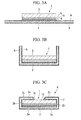
- the tape-shaped oxide superconductor laminate 1 is prepared to which the substrate 3, the interlayer 4, the oxide superconductor layer 5, and the protection layer 6 are laminated, and then the metal tape 2 is arranged under the protection layer 6 of the oxide superconductor laminate 1 as shown in FIG. 3A .
- Solder layers 8 and 9 are formed on the front and the back face of the metal tape 2 by plating. The thickness of the solder layers 8 and 9 is preferably within a range of 1 ⁇ m to 10 ⁇ m, more preferably within a range of 2 ⁇ m to 6 ⁇ m.
- both ends of the metal tape 2 are folded upwardly using a forming roll or the like so as to follow both side faces of the substrate 3 as shown in FIG. 3B .
- the metal tape 2 is further folded so as to follow the top face of the substrate 3 as shown in FIG. 3C .
- the metal tape 2 is folded so as to form substantially a C shape in view of the lateral cross section.
- the whole is heated using a furnace up to the temperature at which the solder layers 8 and 9 are melted. Then, using a pressure roll heated up to a temperature around the melting point of the solder layers 8 and 9, the C shaped metal tape 2 and the oxide superconductor laminate 1 are pressed.
- the melted solder layers 8 and 9 spread so as to completely fill the gap between the oxide superconductor laminate 1 and the metal tape 2 and does fill the gap. After that, the whole is cooled to solidify the solder, and the oxide superconductor wire A as shown in FIG. 3C provided with the solder layer 7 is obtained, which has a structure equal to that shown in FIG. 1 .
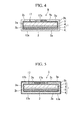
- FIG. 4 and FIG. 5 are a lateral cross-sectional view of the oxide superconductor wires B and C which are a modified example of the oxide superconductor wire A according to the above-described embodiment.
- the oxide superconductor wire B according to the modified example the tape-shaped oxide superconductor laminate 1 is covered with the metal tape 2 in the same way as the oxide superconductor wire A according to the above-described embodiment.
- the oxide superconductor wires B and C according to the present modified examples are different from the oxide superconductor wire A according to the above-described embodiment in that a buried layer 17c formed of a solder layer (low melting point metal layer) 17 fills a gap 11 between the distal edges of the back-side walls 2c and 2c of the C shaped metal tape 2.
- an inner cover layer 17a of the solder layer (low melting point metal layer) 17 is formed only on the inner peripheral face of the metal tape 2 in the oxide superconductor wire B.
- oxide superconductor wires B and C shown in FIG. 4 and FIG. 5 have the same configuration as the oxide superconductor wire A except for the above-described configuration, and the same reference numerals are given to the correspondent components and explanations of those will be omitted.
- the inner cover layer 17a fills the gap between the oxide superconductor laminate 1 and the metal tape 2 and the buried layer 17c fills the gap between the back-side walls 2c and 2c of the metal tape 2.
- the buried layer 17c prevents moisture from permeating into the oxide superconductor laminate 1, and particularly prevents moisture from permeating into the oxide superconductor layer 5 inside the metal tape 2. Even a configuration with the buried layer 17c in which a solder layer is not provided outside the metal tape 2 but the solder layer 17 is provided on the inner face of the metal tape 2 unlike the oxide superconductor wire B will prevent moisture from permeating into the inside.
- solder Using a pressure roll and the other apparatus for supplying solder to the pressure roll, sufficient amount of solder to fill the gap between the back-side walls 2c and 2c of the metal tape 2 is supplied to form the buried layer 17c and thereby the oxide superconductor wires B and C can be obtained.
- it may be arranged to form a thick solder layer on the metal tape 2 in advance, heat the solder layer to melt it, and then cause an overflow of the melted solder from the gap between the back-side walls 2c and 2c the of metal tape 2, using a pressure roll, to form the buried layer 17c.
- the resistance value R of the oxide superconductor wire A in a normal conducting state be within the range shown in the following Equation (1).
- V represents a voltage while Ic represents the critical current value of the oxide superconductor wire A.
- ⁇ is a coefficient multiplied to the critical current value Ic.
- Sufficient transition of the oxide superconductor layer 5 to a normal conducting state requires electric current 1.5 to 3 times the critical current value Ic.
- electric current 1.5 to 3 times the critical current value Ic is applied to the stabilization layer 10 and the protection layer 6. Therefore, the coefficient ⁇ of 1.5 to 3 is multiplied to the critical current value Ic.
- the critical current value Ic of the oxide superconductor layer 5 may be determined depending on the area of the cross section. Practically, for the oxide superconductor wire A having a width of 1 cm, the critical current value Ic is expected to be within a range of 50 to 1000 A.
- the voltage drop of the oxide superconductor wire A having a width of 1cm and a length of 1 cm in a normal conducting state be within a range of 0.3 to 5 V.
- a desirable range of the resistance value R of the oxide superconductor wire A in a normal conducting state can be calculated. Specifically, by substituting 0.3 V for the voltage V, 1000 A for the critical current value Ic, and 3 for the coefficient ⁇ into Equation (1), the lower limit of the resistance value: 100 ⁇ can be obtained. On the other hand, by substituting 5 V for the voltage V, 50 A for the critical current value Ic, and 1.5 for the coefficient ⁇ into the Equation (1), the upper limit of the resistance value: 66.667 m ⁇ can be obtained.
- the oxide superconductor wire A in use is cooled to be around 90 K by liquid nitrogen.
- the resistance value R described above means a resistance value at the temperature in use. Since the resistance value of a normal conductor of a copper alloy (brass, as an example) at room temperature (20°C) is around 1.5 times the resistance value at 90 K, the desirable range of the resistance value of the oxide superconductor wire A at room temperature is no less than 150 ⁇ and no more than 100 m ⁇ . It should be noted that, since the resistance value of the oxide superconductor wire is inversely proportional to its width, the desirable range of the resistance value described above is determined in accordance with the width of the oxide superconductor wire. For example, the desirable range of the resistance value of the oxide superconductor wire having a width of 5 mm and a length of 1 cm at room temperature is no less than 300 ⁇ and no more than 200 m ⁇ .
- the resistance value of the oxide superconductor wire A in a normal conducting state is approximate to the resistance value of the oxide superconductor layer 5 in an insulating state and thus will be the combined resistance of the protection layer 6, the solder layer (low melting point metal layer) 7, 17, and the stabilization layer 10.
- the resistance value of the solder layer 7, 17 is substantially higher than the resistance value of the protection layer 6 and the stabilization layer 10 with consideration of the thickness (i.e., cross section area) and the volume resistivity of the solder layer. More specifically, since electric current hardly flows in the solder layer 7, 17, the contribution of the solder layer 7, 17 is negligible when calculating the resistance value. Therefore, the resistance value of the oxide superconductor wire A in a normal conducting state can be approximated by the combined resistance of the protection layer 6 and the stabilization layer 10.
- the protection layer 6 is made of Ag or an Ag alloy. With the use of the protection layer 6 having a thickness D of 5 ⁇ m or less, it is possible to reduce the cost. In addition, it is preferable that the thickness D of protection layer 6 be 1 ⁇ m or more.
- the resistance value of the stabilization layer 10 may be adjusted in various ways with parameters of the thickness d of the stabilization layer 10 and the volume resistivity of the constituent materials of the stabilization layer 10. Therefore, the thickness d of the stabilization layer 10 and the materials constituting the stabilization layer 10 may be selected such that the resistance value at room temperature of the oxide superconductor wire A, which includes the protection layer 6 having a thickness of no less than 1 ⁇ m and no more than 5 ⁇ m, will be in the range described above.
- the stabilization layer 10 When using a material having a low volume resistivity as the material of the stabilization layer 10, the stabilization layer 10 needs to be thin. However, when forming the metal tape 2 as the stabilization layer 10 on the oxide superconductor laminate 1, tears can occur in the metal tape 2 if the thickness d of the metal tape 2 is too thin. Further, when folding the metal tape 2 in a C shape as described above and form it so as to cover the oxide superconductor laminate 1, tears can occur more easily.
- the stabilization layer 10 when using a material having a high volume resistivity as the material of the stabilization layer 10, the stabilization layer 10 needs to be thick. However, if the stabilization layer 10 is thick, the thickness of the oxide superconductor wire A itself will become enlarged accordingly. Further, when folding the metal tape 2 in a C shape as described above and form it so as to cover the oxide superconductor laminate 1, it is extremely difficult to process the metal tape 2 having a thickness of more than 60 ⁇ m, which requires to apply a high stress to the metal tape 2 during the process and thereby may deteriorate the oxide superconductor layer 5.
- the thickness d of the stabilization layer 10 be no less than 9 ⁇ m and no more than 60 ⁇ m.
- the volume resistivity of the stabilization layer 10 will be no less than 3.8 ⁇ cm and no more than 15 ⁇ cm in order for the resistance value of the oxide superconductor wire A to be no less than 150 ⁇ and no more than 100 m ⁇ .
- the volume resistivity of no less than 3.8 ⁇ cm and no more than 9.6 ⁇ cm is more preferable.
- Examples of the material of the stabilization layer 10 i.e., metal tape 2 satisfying such a volume resistivity include copper nickel alloy (GCN15, GCN10, GCN5: corresponding standard JIS C 2532), Corson alloy, brass (Cu-Zn alloy), beryllium copper, and phosphor bronze.
- Table 1 shows the relationship between the thickness of the protection layer 6 and the thickness of the stabilization layer 10, and the resistance value of the oxide superconductor wire at room temperature (normal conducting state), when using a Corson alloy (C7025) having a volume resistivity of 3.8 ⁇ cm as the material of the stabilization layer 10.
- Table 2 shows the relationship between the thickness of the protection layer 6 and the thickness of the stabilization layer 10, and the resistance value of the oxide superconductor wire at room temperature (normal conducting state), when using a copper nickel alloy (GCN15) having a volume resistivity of 15 ⁇ cm as the material of the stabilization layer 10.
- GCN15 copper nickel alloy
- the volume resistivity of the stabilization layer 10 when the volume resistivity of the stabilization layer 10 is 3.8 ⁇ cm, it is possible to achieve a desirable combined resistance value (i.e., the resistance value of the oxide superconductor wire at room temperature) by adjusting the thickness of the stabilization layer 10 to be in a range of 9.4 to 12.0 ⁇ m to correspond with the protection layer 6 having a thickness of 1 to 5 ⁇ m.
- the volume resistivity of the stabilization layer 10 is 15 ⁇ cm, it is possible to achieve a preferable combined resistance value by adjusting the thickness of the stabilization layer 10 to be in a range of 35.0 to 55.0 ⁇ m.
- the volume resistivity of the stabilization layer 10 is within 3.8 to 15 ⁇ cm, it is possible to obtain an oxide superconductor wire having a preferable resistance value at room temperature by adjusting the thickness of the stabilization layer 10 to be in a range of 9.4 to 58 ⁇ m to correspond with the protection layer 6 having a thickness of 1 to 5 ⁇ m.
- FIG. 6 shows a superconductor current-limiting device 99 using the oxide superconductor wire A (or B, C) described above.
- the oxide superconductor wire A (B, C) is wound in plural layers around a drum to constitute a module 90 for a superconductor current-limiting device.
- the module 90 for a superconductor current-limiting device is housed in a liquid nitrogen tank 95 which is filled with liquid nitrogen 98.
- the liquid nitrogen tank 95 is housed inside a vacuum tank 96 which keeps out heat from outside.
- a liquid nitrogen supply part 91 and a refrigerator 93 are provided on top of the liquid nitrogen tank 95.
- a heat anchor 92 and a heat plate 97 are provided under the refrigerator 93.
- the superconductor current-limiting device 99 includes a current lead part 94 for connecting the module 90 for a superconductor current-limiting device with an external power source (not shown in the figures).
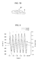
- FIG. 7B shows a pancake coil 101 using the oxide superconductor wire A (B, C) as described above.
- the oxide superconductor wire A may form a wound pancake coil 101. Further, by stacking plural pancake coils 101 and connecting them with one another, it may form a superconductor coil 100 shown in FIG. 7A which will generate strong magnetic force.
- the oxide superconductor wires A, B, and C may be used for various superconductor equipment.
- the superconductor equipment is not particularly limited provided it includes the oxide superconductor wire A, and examples thereof include a superconductor cable, a superconductor motor, a superconductor transformer, a superconductor current-limiting device, and a superconductor electricity storage.
- An Al 2 O 3 layer (diffusion prevention layer; thickness of 150 nm) was formed on a substrate made of tape-shaped HASTELLOY (Trade name, HAYNES INT. INC., USA) having a width of 5 mm and thickness of 0.1 mm by a sputtering method, and a Y 2 O 3 layer (bed layer; thickness of 20 nm) was formed on the diffusion prevention layer by an ion beam sputtering method.
- an MgO layer metal oxide layer; thickness of 10 nm
- IBAD method ion beam assisted deposition method
- CeO 2 cap layer
- PLD method pulse laser deposition method
- a GdBa 2 Cu 3 O 7- ⁇ oxide superconductor layer
- Ag layer protecting layer
- a Sn-solder plated metal tape having a width of 10 mm was folded at both sides of the protection layer to form substantially a C shape in view of the lateral cross section, and the periphery of the oxide superconductor laminate was covered with the metal tape. After that, the Sn solder was melted by heating to form a solder layer such that the metal tape covered and was adhered to the periphery of the oxide superconductor laminate.
- Metal tapes having a thickness and made of a material shown in Table 3 were used.
- the oxide superconductor wires of Examples 1 to 6 and Comparative examples 1 and 2 were subjected to the pressure cooker test in which they were exposed to high temperature (120°C), high humidity (100%), and high pressure (0.2 MPa) for 100 hours, and the ratio of the critical current value before and after the test were measured.
- the percent ratio of the post-exposure critical current value (Ic) to the pre-exposure critical current value (Ic 0 ), which represents moisture derived deterioration is shown in Table 3.
- the metal tape was unable to be formed so as to cover the oxide superconductor laminate in the oxide superconductor wire of Comparative examples 1 and 2. More specifically, as for Comparative example 1, since the thickness 5 ⁇ m of the foil of oxygen free copper used as the metal tape was thin, the metal tape wan torn while forming the metal tape in a C shape and thus the oxide superconductor laminate was unable to be covered.
- the oxide superconductor wires of Comparative examples 1 and 2 were unable to air-tightly cover the oxide superconductor laminate and were thus deteriorated in the pressure cooker test.
- the oxide superconductor wires according to the examples of the present invention exhibited excellent current limiting characteristics. Moreover, in the oxide superconductor wires according to the examples of the present invention, it was confirmed that no moisture derived deterioration occurred even under extreme environmental conditions since the periphery of the oxide superconductor laminate was covered with the metal tape having a certain thickness.
- an oxide superconductor wire for use in superconductor current-limiting devices which is, even if the thickness of the protection layer is reduced, capable of preventing burnout, exhibiting stable current limiting characteristics, and limiting the enlargement of the thickness of the oxide superconductor wire.
Landscapes
- Engineering & Computer Science (AREA)
- Chemical & Material Sciences (AREA)
- Organic Chemistry (AREA)
- Ceramic Engineering (AREA)
- Power Engineering (AREA)
- Inorganic Chemistry (AREA)
- Manufacturing & Machinery (AREA)
- Superconductors And Manufacturing Methods Therefor (AREA)
- Inorganic Compounds Of Heavy Metals (AREA)
- Containers, Films, And Cooling For Superconductive Devices (AREA)
- Emergency Protection Circuit Devices (AREA)
Abstract
Description
- The present invention relates to an oxide superconductor wire used for superconductor equipment such as a superconductor current-limiting device.
- Priority is claimed on Japanese Patent Application No.
2012-288302, filed December 28, 2012 - Electric equipment capable of solving the recent energy challenges includes superconductor equipment such as cable, coil, motor, magnet, and superconductor current-limiting device with the use of an oxide superconductor which is a low-loss electrically conductive material. As a superconductor used for the superconductor equipment, an oxide superconductor such as an RE-123-based oxide superconductor (REBa2Cu3O7-x: RE being a rare-earth element containing Y, Gd etc.) is known. The oxide superconductor exhibits superconductive properties at around the liquid nitrogen temperatures and is capable of maintaining a relatively high critical current density even in a strong magnetic field, and therefore is regarded as an extremely promising electrically conductive material in practice.
- When applying the above-described oxide superconductor to electric equipment, the oxide superconductor is processed to form a wire in general. For example,
Patent Document 1 discloses an oxide superconductor wire using a laminate which includes an oxide superconductor layer formed on a tape-shaped metal substrate via an interlayer having good crystal orientation and a protection layer formed so as to cover the oxide superconductor layer. The outer periphery of the laminate is provided with a stabilization layer formed by covering the outer periphery with a wide-width metal tape via a solder layer. Since the protection layer and the stabilization layer of such an oxide superconductor wire serve to bypass overcurrent in case of emergency, they are formed of low electrical resistance materials. For example, the protection layer may be formed of Ag or an Ag alloy and the stabilization layer may be formed of Cu. - When applying the oxide superconductor wire to superconductor current-limiting devices, in order to increase the electrical resistance in its normal conducting state, it is required to form high electrical resistance materials, as a high-resistance layer, on the oxide superconductor layer. For example,
Patent Document 2 describes the use of metals, as the high-resistance layer formed on the substrate or the oxide superconductor layer, of which the electrical resistivity is no less than 1×10⁻⁷ Ω· m and no more than 1×10⁻⁵ Ω·m at room temperature. -
- [Patent Document 1] Japanese Unexamined Patent Application, First Publication No.
2012-169237 - [Patent Document 2] Japanese Unexamined Patent Application, First Publication No.
2007-227167 - When applying the configuration described in
Patent Document 1, in which the protection layer and the stabilization layer are formed on the oxide superconductor layer, to the oxide superconductor wire for superconductor current-limiting devices, the combined resistance of the protection layer and the stabilization layer is required to be within the resistance value described inPatent Document 2. - Since Ag is a costly material, there is a demand for further reducing the thickness of the protection layer which contains Ag. The protection layer is formed of Ag or an Ag alloy and exhibits significantly lower volume resistivity compared to the stabilization layer. As the thickness of the protection layer is reduced, the thickness of the stabilization layer needs to be considerably thicker to compensate that, which will enlarge the thickness of the oxide superconductor wire. If the thickness of the oxide superconductor wire is enlarged, it will be impossible to increase the magnetic field density of the coil formed by winding the oxide superconductor wire.
- The present invention was made in view of the above-described circumstances and the object thereof is providing an oxide superconductor wire for use in superconductor current-limiting devices, which is, even if the thickness of the protection layer is reduced, capable of preventing burnout, exhibiting stable current limiting characteristics, and limiting the enlargement of the thickness of the oxide superconductor wire.
- An oxide superconductor wire according to the first aspect of the present invention includes: an oxide superconductor laminate including: a tape-shaped substrate, an interlayer laminated on the substrate, an oxide superconductor layer laminated on the interlayer, and a protection layer which is formed of Ag or an Ag alloy and laminated on the oxide superconductor layer; and a stabilization layer which is formed of a metal tape and formed on the protection layer of the superconductor laminate via a low melting point metal layer, wherein the thickness of the protection layer is 5 µm or less, and wherein a volume resistivity of the stabilization layer at room temperature is no less than 3.8 µΩ·cm and no more than 15 µΩ·cm.
- According to the first aspect, since the thickness of the protection layer formed of Ag or an Ag alloy is 5 µm or less, it is possible to reduce the amount of Ag used for the oxide superconductor wire, and thereby reduce the cost. In addition, since the volume resistivity of the metal tape at room temperature is no less than 3.8 µΩ·cm and no more than 15 µΩ·cm, it is possible, even when electric current 1.5-3 times the critical current is applied, to limit the excessive current and thereby prevent burnout of the oxide superconductor wire and achieve stable current limiting characteristics in superconductor current-limiting devices using the oxide superconductor wire even with the thickness of the protection layer of 5 µm or less.
- Additionally, an oxide superconductor wire according to the second aspect of the present invention includes: a tape-shaped substrate, an interlayer laminated on the substrate, an oxide superconductor layer laminated on the interlayer, and a protection layer which is formed of Ag or an Ag alloy and laminated on the oxide superconductor layer; and a stabilization layer which is formed of a metal tape and formed on the protection layer of the superconductor laminate via a low melting point metal layer, wherein the thickness of the protection layer is 5 µm or less, and wherein a resistance value of the oxide superconductor wire per 1 cm width and 1 cm length at room temperature is no less than 150 µΩ and no more than 100 mΩ.
- According to the second aspect, since the thickness of the protection layer formed of Ag or an Ag alloy is 5 µm or less, it is possible to reduce the amount of Ag used for the oxide superconductor wire, and thereby to reduce the cost. In addition, since the resistance value of the oxide superconductor wire per 1 cm width and 1 cm length at room temperature is no less than 150 µΩ and no more than 100 mΩ, it is possible, even when electric current 1.5-3 times the critical current is applied, to limit the excessive current and thereby prevent the burnout of the oxide superconductor wire and achieve stable current limiting characteristics in superconductor current-limiting devices using the oxide superconductor wire even with the thickness of the protection layer of 5 µm or less.
- It may be arranged such that a width of the metal tape constituting the stabilization layer is greater than the width of the oxide superconductor laminate, and a top face of the protection layer of the oxide superconductor laminate, side faces of the protection layer, the oxide superconductor layer, the interlayer and the substrate, and at least a part of a back face of the substrate are covered with the stabilization layer via the low melting point metal layer.
- In this case, since the outer periphery of the oxide superconductor laminate is covered with the metal tape, it possible to prevent the oxide superconductor layer from deteriorating due to intrusion of moisture.
- It may be arranged such that the thickness of the stabilization layer is no less than 9 µm and no more than 60 µm.
- In this case, the thickness of the stabilization layer is no less than 9 µm and no more than 60 µm. More specifically, the thickness of the metal tape covering the oxide superconductor laminate is no less than 9 µm and no more than 60 µm. With the metal tape having a thickness of no less than 9 µm, it is possible to prevent the metal tape from tearing in the process of covering the oxide superconductor laminate with the metal tape. Moreover, the metal tape having a thickness of 60 µm or less will facilitate the forming of the metal tape and reliably cover the oxide superconductor laminate.
- A superconductor coil according to the third aspect of the present invention includes the oxide superconductor wire described above.
- A superconductor current-limiting device according to the fourth aspect of the present invention includes the oxide superconductor wire described above.
- A superconductor equipment according to the fifth aspect of the present invention includes the oxide superconductor wire described above.
- With the use of the oxide superconductor wire in superconductor coils, superconductor current-limiting devices, and the other superconductor equipment, it is possible to enhance the protection performance of the superconductor equipment with respect to moisture. In addition, it is possible to prevent the burnout of the oxide superconductor wire when excessive current flows in the oxide superconductor wire. Accordingly, it is possible to achieve more reliable superconductor equipment compared to the conventional one.
- According to the above-described aspect of the present invention, since the thickness of the protection layer formed of Ag or an Ag alloy is 5 µm or less, it is possible to reduce the amount of Ag used for the oxide superconductor wire, and thereby reduce the cost. In addition, since the volume resistivity of the metal tape at room temperature is no less than 3.8 µΩ·cm and no more than 15 µΩ·cm, it is possible, even when electric current 1.5-3 times the critical current is applied, to limit the excessive current, and thereby prevent burnout of the oxide superconductor wire and achieve stable current limiting characteristics in superconductor current-limiting devices using the oxide superconductor wire even with the thickness of the protection layer of 5 µm or less.
-
-
FIG. 1 is a perspective view showing a lateral cross section of the oxide superconductor wire according to an embodiment of the present invention. -
FIG. 2 is a perspective view showing a partial cross section of an example of the oxide superconductor laminate arranged in the oxide superconductor wire shown inFIG. 1 . -
FIG. 3A is a cross-sectional view showing a state where the metal tape is arranged under the oxide superconductor laminate in an example of a manufacturing method of the oxide superconductor wire shown inFIG. 1 . -
FIG. 3B is a cross-sectional view showing a state where the metal tape arranged under the oxide superconductor laminate is bent in an example of a manufacturing method of the oxide superconductor wire shown inFIG. 1 . -
FIG. 3C is a cross-sectional view showing a state where the metal tape is soldered to the oxide superconductor laminate in an example of a manufacturing method of the oxide superconductor wire shown inFIG. 1 . -
FIG. 4 is a lateral cross-sectional view showing a modified example of the oxide superconductor wire according to the embodiment. -
FIG. 5 is a lateral cross-sectional view showing a modified example of the oxide superconductor wire according to the embodiment. -
FIG. 6 is a cross-sectional view showing an example of a superconductor current-limiting device. -
FIG. 7A is a perspective view showing an embodiment of a laminate of a superconductor coil. -
FIG. 7B is a perspective view showing an embodiment of a superconductor coil. -
FIG. 8 is a graph showing the suppression of fault current obtained by the oxide superconductor wire. - Hereinafter, oxide superconductor wires according to embodiments of the present invention will be described with reference to the drawings. It should be noted that, in the drawings, some parts are magnified in shape for the purpose of explanation, but the proportions, for example, of the components shown in the drawings are not necessarily the same as the actual ones.
-
FIG. 1 is a perspective view showing a lateral cross section of the oxide superconductor wire according to an embodiment of the present invention. An oxide superconductor wire A according to the embodiment includes a tape-shapedoxide superconductor laminate 1 and ametal tape 2 formed of an electrically conductive material such as a copper and covering theoxide superconductor laminate 1. - The
oxide superconductor laminate 1 includes a tape-shapedsubstrate 3, an interlayer 4, anoxide superconductor layer 5, and aprotection layer 6 as shown inFIG. 2 . The interlayer 4, theoxide superconductor layer 5, and theprotection layer 6 are laminated onto thesubstrate 3 in this order. - Hereinafter, each component of the
oxide superconductor laminate 1 will be described in detail based onFIG. 2 . - The
substrate 3 may be one which is capable of being used for a substrate of common oxide superconductor wires and preferably has flexibility and elongated tape shape. In addition, the material of thesubstrate 3 preferably contains a metal which has high mechanical strength and heat resistance and can be easily processed into wires. Examples of such materials includes, for example, various kinds of heat-resistance metal materials including a nickel alloy such as stainless steel and HASTELLOY, and materials having ceramics arranged on the various kinds of metal materials. In particular, HASTELLOY (Trade name, HAYNES INT. INC., USA) is preferable among commercially available products. Various kinds of HASTELLOY such as HASTELLOY B, C, G, N, and W are available, which contain different amount of ingredients such as molybdenum, chromium, iron, and cobalt. Any of the HASTELLOYs can be used for thesubstrate 3. Alternatively, for thesubstrate 3, an oriented Ni-W alloy tape substrate may be employed, the substrate being formed by introducing texture into a nickel alloy. The thickness of thesubstrate 3 may be adjusted in accordance with the purpose, typically be 10 to 500 µm, and preferably be 20 to 200 µm. - An example of the interlayer 4 may have a configuration in which a diffusion prevention layer, a bed layer, an orientation layer, and a cap layer are laminated in this order.
- The diffusion prevention layer will serve to prevent part of the constituent elements of the
substrate 3 from diffusing and being admixed, as impurities, into theoxide superconductor layer 5, when heat treatment is performed to the layers formed above the diffusion prevention layer and, as a result, imparts thermal hysteresis to thesubstrate 3 and the other layers. The specific structure of the diffusion prevention layer is not particularly limited provided it is capable of providing the above-described effects. It is preferable to employ a diffusion prevention layer having a single-layer or multilayer structure constituted by Al2O3, Si3N4, GZO (Gd2Zr2O7), or the like, which are relatively effective in preventing the admixture of impurities. - The bed layer is used to prevent reactions of the constituent element at the interface between the
substrate 3 and theoxide superconductor layer 5 and improve the orientation of layers which are provided on the bed layer. The specific structure of the bed layer is not particularly limited provided it is capable of providing the above-described effects. It is preferable to employ a bed layer having single-layer or multilayer structure constituted by a rare earth oxide which have high heat resistance, such as Y2O3, CeO2, La2O3, Dy2O3, Er2O3, Eu2O3, and Ho2O3. - The orientation layer serves to control the crystal orientation of the cap layer and the
oxide superconductor layer 5 which are formed thereon, prevent the constituent elements of thesubstrate 3 from diffusing into theoxide superconductor layer 5, and mitigate the difference between thesubstrate 3 and theoxide superconductor layer 5 in terms of physical characteristics such as coefficient of thermal expansion and lattice constant. The material of the orientation layer is not particularly limited provided it is capable of providing the above-described effects, but is preferably a metal oxide such as Gd2Zr2O7, MgO, ZrO2-Y2O3 (YSZ), and the like. When using such a metal oxide as the material of the orientation layer, a layer having high crystal orientation can be obtained with an ion beam assisted deposition method (hereinafter, may be referred to as IBAD method) which is described later, which will further improve the crystal orientation of the cap layer and theoxide superconductor layer 5. - The cap layer serves to strongly control the crystal orientation of the
oxide superconductor layer 5 equally or more than the orientation layer, prevent the constituent elements of theoxide superconductor layer 5 from diffusing into the interlayer 4, and prevent reactions between the interlayer 4 and gases used in the process of laminating theoxide superconductor layer 5. - The material of the cap layer is not particularly limited provided it is capable of providing above-described effects, but is preferably a metal oxide such as CeO2, LaMnO3, Y2O3, Al2O3, Gd2O3, ZrO2, Ho2O3, Nd2O3, and Zr2O3, in view of lattice matching with respect to the
oxide superconductor layer 5. Of these materials, CeO2 and LaMnO3 are particularly preferable in view of the matching with respect to theoxide superconductor layer 5. - When using CeO2 as the material of the cap layer, the cap layer may include a Ce-M-O based oxide in which part of Ce atoms are substituted with the other metal atoms or metal ions.
- The
oxide superconductor layer 5 serves to conduct an electric current when it is in a superconducting state. Wide variety of oxide superconductor materials having commonly-known compositions may be employed as the material of theoxide superconductor layer 5. Examples thereof include a copper oxide superconductor such as RE-123 based superconductor and Bi based superconductor. Examples of the composition of the RE-123 based superconductor include REBa2Cu3O(7-x) (RE represents a rare-earth element such as Y, La, Nd, Sm, Er, and Gd while x represents deficient oxygen), more particularly Y123 (YBa2Cu3O(7-x)) and Gd123 (GdBa2Cu3O(7-x)). Examples of the composition of the Bi based superconductor include Bi2Sr2Can-1CunO4+2n+δ (n represents the number of CuO2 layers while δ represents excess oxygen). With respect to the copper oxide superconductor, introduction of oxygen through oxygen annealing into its original material, which is an insulator, will give an oxide superconductor having a well-organized crystal structure and exhibiting superconductive properties. - In the present embodiment, a copper oxide superconductor is used as the material of the
oxide superconductor layer 5, and unless otherwise stated, the material of theoxide superconductor layer 5 is a copper oxide superconductor hereinafter. - The
protection layer 6 serves to bypass overcurrent (fault current) generated in case of emergency (e.g., short circuit by lightning strike etc.) together with a later-describedstabilization layer 10, prevent chemical reactions between theoxide superconductor layer 5 and other layers provided thereon, and prevent the deterioration of the superconductive properties due to admixture of part of atoms of one of the laminated layers into another layer to cause perturbation of the composition of the layer. In addition, theprotection layer 6 has oxygen permeability when heating, which allows oxygen to be easily introduced into theoxide superconductor layer 5. - In this regard, it is preferable that the
protection layer 6 be formed of Ag or other materials including at least Ag, such as an Ag alloy. - It should be noted that the
protection layer 6 is arranged only on the top face of theoxide superconductor layer 5 inFIG. 1 and FIG. 2 , but the configuration is not limited to this. When forming theprotection layer 6 with a film formation method such as a sputtering method, a thin Ag layer may be formed on at least one of the side faces of thesubstrate 3, the interlayer 4, theoxide superconductor layer 5, and the back face of thesubstrate 3 due to scattering around of Ag particles. Such a configuration may be employed. - The thickness D of the
protection layer 6 formed on theoxide superconductor layer 5 may be 5 µm or less. When the thickness D of theprotection layer 6 is 5 µm or less, it is possible to reduce the cost. In addition, the thickness D of theprotection layer 6 is preferably 1 µm or more. If the thickness D of theprotection layer 6 is less than 1 µm, Ag will be aggregated and theoxide superconductor layer 5 could be exposed from theprotection layer 6 during the oxygen annealing of theprotection layer 6. In the later-describedstabilization layer 10 formed by covering theprotection layer 6 with themetal tape 2 via thesolder layer 7, part of Ag of theprotection layer 6 will be absorbed by the solder. This means, the metal materials constituting the solder will diffuse into theprotection layer 6 of Ag and the resistance value of theprotection layer 6 of Ag will increase. - The
oxide superconductor laminate 1 is configured as described above. - Next, the oxide superconductor wire A, in which the outer periphery of the above-described
oxide superconductor laminate 1 is covered with themetal tape 2, will be described based onFIG. 1 . - The
metal tape 2 formed of an electrically conductive material such as a copper is arranged so as to cover the front face and both side faces of theprotection layer 6, both side faces of theoxide superconductor layer 5 under theprotection layer 6, both side faces of the interlayer 4, both side faces of thesubstrate 3, and part of the back face of thesubstrate 3 and thus themetal tape 2 forms thestabilization layer 10. - The
stabilization layer 10 serves as a bypass to commutate electric current together with theprotection layer 6 when theoxide superconductor layer 5 transitions from a superconducting state into a normal conducting state. - Both front and back face of the
metal tape 2 is provided with the solder layer (low melting point metal layer) 7. Thesolder layer 7 includes anouter cover layer 7a covering the outer periphery of themetal tape 2, theinner cover layer 7b being tightly attached to the inner face of themetal tape 2 and covering the periphery of theoxide superconductor laminate 1, and thecover part 7c covering both ends, in the width direction, of themetal tape 2. - The
metal tape 2 is bent to form, in view of the lateral cross section, substantially a C shape having a front-side wall 2a, a lateral-side wall 2b, and a back-side wall protection layer 6 to the back face of thesubstrate 3 to cover theoxide superconductor laminate 1 so as to expose part of the back face of thesubstrate 3. In other words, themetal tape 2 covers the top face and both side faces of theprotection layer 6, both side faces of theoxide superconductor layer 5, both side faces of the interlayer 4, both side faces of thesubstrate 3, and the back face of thesubstrate 3. - The
inner cover layer 7b of thesolder layer 7 is formed so as to completely fill the gap between themetal tape 2 and theoxide superconductor laminate 1 in the entire peripheral face of theoxide superconductor laminate 1. - The solder layer (low melting point metal layer) 7 of the present embodiment is formed of solder, but the low melting point metal layer may be formed of a metal having a melting point within a range of 240 to 400°C such as Sn, Sn alloy, and indium. The above-described solder may be Sn-Pb based, Pb-Sn-Sb based, Sn-Pb-Bi based, Bi-Sn based, Sn-Cu based, Sn-Pb-Cu based, Sn-Ag based solder etc.. It should be noted that, since the
solder layer 7 with high melting point will adversely affect the superconductive properties of theoxide superconductor layer 5 when melting thesolder layer 7, it is preferable that the melting point of thesolder layer 7 be lower. Specifically, it is preferable to use a material having a melting point of 350°C or less, more preferably within a range of approximately 240 to 300°C. - It is preferable that the thickness of the
solder layer 7 be within a range of 1 µm to 10 µm, more preferably within a range of 2 µm to 6 µm. If the thickness of thesolder layer 7 is less than 1 µm, the gap between theoxide superconductor laminate 1 and themetal tape 2 may not be completely filled, which will leave the gap. In addition, an alloy layer may be formed between thesolder layer 7 and themetal tape 2 or between thesolder layer 7 and theprotection layer 6 of Ag due to the diffusion of the constituent elements of thesolder layer 7 during the melting of the solder. On the other hand, if the thickness of thesolder layer 7 is more than 10 µm, a large amount of the solder will be overflowed from the distal end of the back-side wall 2c of themetal tape 2 when performing soldering by heating and pressing the solder, with rolls as described later, to melt the solder. As a result, the thickness of thecover part 7c will become larger, which will cause irregular winding when winding the oxide superconductor wire A. - In the oxide superconductor wire A shown in
FIG. 1 , since thesolder layer 7 filling the gap between theoxide superconductor laminate 1 and itsperipheral metal tape 2 covers the periphery of theoxide superconductor laminate 1, it is possible to prevent outside moisture from permeating into theoxide superconductor laminate 1 arranged inside themetal tape 2. - In manufacturing the oxide superconductor wire A shown in
FIG. 1 , the tape-shapedoxide superconductor laminate 1 is prepared to which thesubstrate 3, the interlayer 4, theoxide superconductor layer 5, and theprotection layer 6 are laminated, and then themetal tape 2 is arranged under theprotection layer 6 of theoxide superconductor laminate 1 as shown inFIG. 3A . Solder layers 8 and 9 are formed on the front and the back face of themetal tape 2 by plating. The thickness of the solder layers 8 and 9 is preferably within a range of 1 µm to 10 µm, more preferably within a range of 2 µm to 6 µm. - After aligning the positions of the center of the
oxide superconductor laminate 1 and the center of themetal tape 2, both ends of themetal tape 2 are folded upwardly using a forming roll or the like so as to follow both side faces of thesubstrate 3 as shown inFIG. 3B . Then, themetal tape 2 is further folded so as to follow the top face of thesubstrate 3 as shown inFIG. 3C . As described above, themetal tape 2 is folded so as to form substantially a C shape in view of the lateral cross section. - After the folding described above, the whole is heated using a furnace up to the temperature at which the solder layers 8 and 9 are melted. Then, using a pressure roll heated up to a temperature around the melting point of the solder layers 8 and 9, the C shaped
metal tape 2 and theoxide superconductor laminate 1 are pressed. - Through this process, the melted
solder layers oxide superconductor laminate 1 and themetal tape 2 and does fill the gap. After that, the whole is cooled to solidify the solder, and the oxide superconductor wire A as shown inFIG. 3C provided with thesolder layer 7 is obtained, which has a structure equal to that shown inFIG. 1 . -
FIG. 4 and FIG. 5 are a lateral cross-sectional view of the oxide superconductor wires B and C which are a modified example of the oxide superconductor wire A according to the above-described embodiment. In the oxide superconductor wire B according to the modified example, the tape-shapedoxide superconductor laminate 1 is covered with themetal tape 2 in the same way as the oxide superconductor wire A according to the above-described embodiment. - The oxide superconductor wires B and C according to the present modified examples are different from the oxide superconductor wire A according to the above-described embodiment in that a buried
layer 17c formed of a solder layer (low melting point metal layer) 17 fills agap 11 between the distal edges of the back-side walls metal tape 2. In addition, aninner cover layer 17a of the solder layer (low melting point metal layer) 17 is formed only on the inner peripheral face of themetal tape 2 in the oxide superconductor wire B. - The oxide superconductor wires B and C shown in
FIG. 4 and FIG. 5 have the same configuration as the oxide superconductor wire A except for the above-described configuration, and the same reference numerals are given to the correspondent components and explanations of those will be omitted. - In the oxide superconductor wires B and C shown in
FIG. 4 and FIG. 5 , theinner cover layer 17a fills the gap between theoxide superconductor laminate 1 and themetal tape 2 and the buriedlayer 17c fills the gap between the back-side walls metal tape 2. The buriedlayer 17c prevents moisture from permeating into theoxide superconductor laminate 1, and particularly prevents moisture from permeating into theoxide superconductor layer 5 inside themetal tape 2. Even a configuration with the buriedlayer 17c in which a solder layer is not provided outside themetal tape 2 but thesolder layer 17 is provided on the inner face of themetal tape 2 unlike the oxide superconductor wire B will prevent moisture from permeating into the inside. - Using a pressure roll and the other apparatus for supplying solder to the pressure roll, sufficient amount of solder to fill the gap between the back-
side walls metal tape 2 is supplied to form the buriedlayer 17c and thereby the oxide superconductor wires B and C can be obtained. Alternatively, it may be arranged to form a thick solder layer on themetal tape 2 in advance, heat the solder layer to melt it, and then cause an overflow of the melted solder from the gap between the back-side walls metal tape 2, using a pressure roll, to form the buriedlayer 17c. - Hereinafter, the electrical properties of the above-described oxide superconductor wire A (B, C) according to the embodiment of the present invention will be described.
- When the oxide superconductor wire A is applied to a superconductor current-limiting device, it is preferable that the resistance value R of the oxide superconductor wire A in a normal conducting state be within the range shown in the following Equation (1).
- [Equation 1]

- In the Equation (1), V represents a voltage while Ic represents the critical current value of the oxide superconductor wire A. α is a coefficient multiplied to the critical current value Ic. Sufficient transition of the
oxide superconductor layer 5 to a normal conducting state requires electric current 1.5 to 3 times the critical current value Ic. In other words, when theoxide superconductor layer 5 transitions from a superconducting state to a normal conducting state, electric current 1.5 to 3 times the critical current value Ic is applied to thestabilization layer 10 and theprotection layer 6. Therefore, the coefficient α of 1.5 to 3 is multiplied to the critical current value Ic. - The critical current value Ic of the
oxide superconductor layer 5 may be determined depending on the area of the cross section. Practically, for the oxide superconductor wire A having a width of 1 cm, the critical current value Ic is expected to be within a range of 50 to 1000 A. - It should be noted that, in order to achieve current limiting characteristics, it is required that the voltage drop of the oxide superconductor wire A having a width of 1cm and a length of 1 cm in a normal conducting state be within a range of 0.3 to 5 V.
- By substituting values of the critical current value Ic, the voltage V, and the coefficient α in the above-described range into the Equation (1), a desirable range of the resistance value R of the oxide superconductor wire A in a normal conducting state can be calculated. Specifically, by substituting 0.3 V for the voltage V, 1000 A for the critical current value Ic, and 3 for the coefficient α into Equation (1), the lower limit of the resistance value: 100 µΩ can be obtained. On the other hand, by substituting 5 V for the voltage V, 50 A for the critical current value Ic, and 1.5 for the coefficient α into the Equation (1), the upper limit of the resistance value: 66.667 mΩ can be obtained.
- The oxide superconductor wire A in use is cooled to be around 90 K by liquid nitrogen. The resistance value R described above means a resistance value at the temperature in use. Since the resistance value of a normal conductor of a copper alloy (brass, as an example) at room temperature (20°C) is around 1.5 times the resistance value at 90 K, the desirable range of the resistance value of the oxide superconductor wire A at room temperature is no less than 150 µΩ and no more than 100 mΩ. It should be noted that, since the resistance value of the oxide superconductor wire is inversely proportional to its width, the desirable range of the resistance value described above is determined in accordance with the width of the oxide superconductor wire. For example, the desirable range of the resistance value of the oxide superconductor wire having a width of 5 mm and a length of 1 cm at room temperature is no less than 300 µΩ and no more than 200 mΩ.
- The resistance value of the oxide superconductor wire A in a normal conducting state is approximate to the resistance value of the
oxide superconductor layer 5 in an insulating state and thus will be the combined resistance of theprotection layer 6, the solder layer (low melting point metal layer) 7, 17, and thestabilization layer 10. Of these, the resistance value of thesolder layer protection layer 6 and thestabilization layer 10 with consideration of the thickness (i.e., cross section area) and the volume resistivity of the solder layer. More specifically, since electric current hardly flows in thesolder layer solder layer protection layer 6 and thestabilization layer 10. - The
protection layer 6 is made of Ag or an Ag alloy. With the use of theprotection layer 6 having a thickness D of 5 µm or less, it is possible to reduce the cost. In addition, it is preferable that the thickness D ofprotection layer 6 be 1 µm or more. - The resistance value of the
stabilization layer 10 may be adjusted in various ways with parameters of the thickness d of thestabilization layer 10 and the volume resistivity of the constituent materials of thestabilization layer 10. Therefore, the thickness d of thestabilization layer 10 and the materials constituting thestabilization layer 10 may be selected such that the resistance value at room temperature of the oxide superconductor wire A, which includes theprotection layer 6 having a thickness of no less than 1 µm and no more than 5 µm, will be in the range described above. - When using a material having a low volume resistivity as the material of the
stabilization layer 10, thestabilization layer 10 needs to be thin. However, when forming themetal tape 2 as thestabilization layer 10 on theoxide superconductor laminate 1, tears can occur in themetal tape 2 if the thickness d of themetal tape 2 is too thin. Further, when folding themetal tape 2 in a C shape as described above and form it so as to cover theoxide superconductor laminate 1, tears can occur more easily. - On the other hand, when using a material having a high volume resistivity as the material of the
stabilization layer 10, thestabilization layer 10 needs to be thick. However, if thestabilization layer 10 is thick, the thickness of the oxide superconductor wire A itself will become enlarged accordingly. Further, when folding themetal tape 2 in a C shape as described above and form it so as to cover theoxide superconductor laminate 1, it is extremely difficult to process themetal tape 2 having a thickness of more than 60 µm, which requires to apply a high stress to themetal tape 2 during the process and thereby may deteriorate theoxide superconductor layer 5. - In view of the above, it is preferable that the thickness d of the
stabilization layer 10 be no less than 9 µm and no more than 60 µm. In this range of the thickness d, the volume resistivity of thestabilization layer 10 will be no less than 3.8 µΩ·cm and no more than 15 µΩ·cm in order for the resistance value of the oxide superconductor wire A to be no less than 150 µΩ and no more than 100 mΩ. The volume resistivity of no less than 3.8 µΩ·cm and no more than 9.6 µΩ·cm is more preferable. - Examples of the material of the stabilization layer 10 (i.e., metal tape 2) satisfying such a volume resistivity include copper nickel alloy (GCN15, GCN10, GCN5: corresponding standard JIS C 2532), Corson alloy, brass (Cu-Zn alloy), beryllium copper, and phosphor bronze.
- Table 1 shows the relationship between the thickness of the
protection layer 6 and the thickness of thestabilization layer 10, and the resistance value of the oxide superconductor wire at room temperature (normal conducting state), when using a Corson alloy (C7025) having a volume resistivity of 3.8 µΩ·cm as the material of thestabilization layer 10. - On the other hand, Table 2 shows the relationship between the thickness of the
protection layer 6 and the thickness of thestabilization layer 10, and the resistance value of the oxide superconductor wire at room temperature (normal conducting state), when using a copper nickel alloy (GCN15) having a volume resistivity of 15 µΩ·cm as the material of thestabilization layer 10.[Table 1] Protection layer Stabilization layer Oxide superconductor wire Ag C7025 Corson alloy (volume resistivity of 3.8 µΩ·cm) Resistance value (room temperature, 1cm width, 1 cm long) Layer thickness Thickness 1 µm 12.0 µm 1.26 mΩ 3 µm 11.5 µm 1.14 mΩ 5 µm 9.4 µm 1.14 mΩ [Table 2] Protection layer Stabilization layer Oxide superconductor wire Ag GCN 15 Copper nickel alloy (volume resistivity of 15 µΩ·cm) Resistance value (room temperature, 1cm width, 1 cm long) Layer thickness Thickness 1 µm 55.0 µm 1.12 mΩ 3 µm 45.0 µm 1.31 mΩ 5 µm 35.0 µm 1.17 mΩ - As will be appreciated from Table 1, when the volume resistivity of the
stabilization layer 10 is 3.8 µΩ·cm, it is possible to achieve a desirable combined resistance value (i.e., the resistance value of the oxide superconductor wire at room temperature) by adjusting the thickness of thestabilization layer 10 to be in a range of 9.4 to 12.0 µm to correspond with theprotection layer 6 having a thickness of 1 to 5 µm. Similarly, as will be appreciated from Table 2, when the volume resistivity of thestabilization layer 10 is 15 µΩ·cm, it is possible to achieve a preferable combined resistance value by adjusting the thickness of thestabilization layer 10 to be in a range of 35.0 to 55.0 µm. - In view of the above, when the volume resistivity of the
stabilization layer 10 is within 3.8 to 15 µΩ·cm, it is possible to obtain an oxide superconductor wire having a preferable resistance value at room temperature by adjusting the thickness of thestabilization layer 10 to be in a range of 9.4 to 58 µm to correspond with theprotection layer 6 having a thickness of 1 to 5 µm. -
FIG. 6 shows a superconductor current-limiting device 99 using the oxide superconductor wire A (or B, C) described above. - In the superconductor current-limiting device 99, the oxide superconductor wire A (B, C) is wound in plural layers around a drum to constitute a
module 90 for a superconductor current-limiting device. Themodule 90 for a superconductor current-limiting device is housed in aliquid nitrogen tank 95 which is filled withliquid nitrogen 98. Theliquid nitrogen tank 95 is housed inside avacuum tank 96 which keeps out heat from outside. - A liquid
nitrogen supply part 91 and arefrigerator 93 are provided on top of theliquid nitrogen tank 95. Aheat anchor 92 and aheat plate 97 are provided under therefrigerator 93. - In addition, the superconductor current-limiting device 99 includes a current
lead part 94 for connecting themodule 90 for a superconductor current-limiting device with an external power source (not shown in the figures). -
FIG. 7B shows apancake coil 101 using the oxide superconductor wire A (B, C) as described above. The oxide superconductor wire A may form awound pancake coil 101. Further, by stacking plural pancake coils 101 and connecting them with one another, it may form asuperconductor coil 100 shown inFIG. 7A which will generate strong magnetic force. - As is explained above, the oxide superconductor wires A, B, and C may be used for various superconductor equipment. It should be noted that the superconductor equipment is not particularly limited provided it includes the oxide superconductor wire A, and examples thereof include a superconductor cable, a superconductor motor, a superconductor transformer, a superconductor current-limiting device, and a superconductor electricity storage.
- Hereinafter, embodiments of the present invention will be described in detail with the use of examples, but the present invention is not limited to the examples.
- An Al2O3 layer (diffusion prevention layer; thickness of 150 nm) was formed on a substrate made of tape-shaped HASTELLOY (Trade name, HAYNES INT. INC., USA) having a width of 5 mm and thickness of 0.1 mm by a sputtering method, and a Y2O3 layer (bed layer; thickness of 20 nm) was formed on the diffusion prevention layer by an ion beam sputtering method. Then, an MgO layer (metal oxide layer; thickness of 10 nm) was formed on the bed layer by an ion beam assisted deposition method (IBAD method) and a CeO2 (cap layer) having a thickness of 0.5 µm was formed on the metal oxide layer by a pulse laser deposition method (PLD method). After that, a GdBa2Cu3O7-δ (oxide superconductor layer) having a thickness of 2.0 µm was formed on the cap layer by PLD method and an Ag layer (protection layer) having a thickness of 5 µm was formed on the oxide superconductor layer by a sputtering method. In addition, a Sn-solder plated metal tape having a width of 10 mm was folded at both sides of the protection layer to form substantially a C shape in view of the lateral cross section, and the periphery of the oxide superconductor laminate was covered with the metal tape. After that, the Sn solder was melted by heating to form a solder layer such that the metal tape covered and was adhered to the periphery of the oxide superconductor laminate. Metal tapes having a thickness and made of a material shown in Table 3 were used. Through the process described above, oxide superconductor wires of Examples 1 to 6 and Comparative examples 1 and 2 were obtained.
- The oxide superconductor wires of Examples 1 to 6 and Comparative examples 1 and 2 were subjected to the pressure cooker test in which they were exposed to high temperature (120°C), high humidity (100%), and high pressure (0.2 MPa) for 100 hours, and the ratio of the critical current value before and after the test were measured. For each oxide superconductor wire, the percent ratio of the post-exposure critical current value (Ic) to the pre-exposure critical current value (Ic0), which represents moisture derived deterioration, is shown in Table 3.
- In addition, as to the current limiting characteristics, the suppression performance of excessive current in case of emergency was confirmed as follows. Each of the oxide superconductor wires of Examples 1 to 6 and Comparative examples 1 and 2 was cut into 10 cm long, and excessive current equivalent to the expected extraordinary current was applied between both ends of the wire. The waveform of the electric current from immediately after the application of the electric current to the sixth wave was observed to confirm whether or not the current limiting effect was obtained for each wire. The results are shown in Table 3. It should be noted that "O" in the table represents that the metal tape was able to be formed while "X" represents that the metal tape was unable to be formed. In addition, an exemplary example of the waveform of the electric current is shown in
FIG. 8 , which was measured when excessive current equivalent to the expected fault current was applied to the oxide superconductor wire of Example 2.[Table 3] Metal tape Volume resistivity Foil thickness Formability Moisture derived deterioration Current limiting characteristics (µΩ·cm) (µm) Ic/Ic0 Comparative example 1 C1020R Oxygen free copper 1.7 5 X 100% O Example 1 C7025 Corson alloy 3.8 10 O 0% O Example 2 GCN5 Cupronickel 5.0 15 O 0% O Example 3 C2680R Brass 6.4 20 O 0% O Example 4 C1720R Beryllium alloy 9.6 30 O 0% O Example 5 C5191R Phosphor bronze 13 40 O 0% O Example 6 GCN15 Cupronickel 15 50 O 0% O Comparative example 2 C7521R Nickel silver 29 96 X *30% *O - As shown in Table 3, the metal tape was unable to be formed so as to cover the oxide superconductor laminate in the oxide superconductor wire of Comparative examples 1 and 2. More specifically, as for Comparative example 1, since the
thickness 5 µm of the foil of oxygen free copper used as the metal tape was thin, the metal tape wan torn while forming the metal tape in a C shape and thus the oxide superconductor laminate was unable to be covered. - On the other hand, as for Comparative example 2, since the nickel silver used as the metal tape has high rigidity and the
foil thickness 96 µm was thick, the metal tape made of a nickel silver was unable to be formed in a C shape. - Accordingly, as for the moisture derived deterioration and the current limiting characteristics of Comparative examples 1 and 2, evaluations were performed for wires in which the metal tape which has a thickness of twice the foil thickness described in Table 3 was formed on the protection layer of the oxide superconductor laminate via the solder layer form.
- The oxide superconductor wires of Comparative examples 1 and 2 were unable to air-tightly cover the oxide superconductor laminate and were thus deteriorated in the pressure cooker test.
- In contrast, the oxide superconductor wires of Examples 1 to 6 were not deteriorated in the pressure cooker test.
- It should be noted that all the oxide superconductor wires of Examples 1 to 6 and Comparative examples 1 and 2 exhibited excellent current limiting characteristics. With reference to the exemplary example of the waveform of the electric current measured for the wire of Example 2 shown in
FIG. 8 , it is observed that the current value is gradually reduced from the first wave. - As described above, it was confirmed that the oxide superconductor wires according to the examples of the present invention exhibited excellent current limiting characteristics. Moreover, in the oxide superconductor wires according to the examples of the present invention, it was confirmed that no moisture derived deterioration occurred even under extreme environmental conditions since the periphery of the oxide superconductor laminate was covered with the metal tape having a certain thickness.
- According to the embodiments of the present invention, it is possible to provide an oxide superconductor wire for use in superconductor current-limiting devices, which is, even if the thickness of the protection layer is reduced, capable of preventing burnout, exhibiting stable current limiting characteristics, and limiting the enlargement of the thickness of the oxide superconductor wire.
-
- 1
- Oxide superconductor laminate
- 2
- Metal tape
- 3
- Substrate
- 4
- Interlayer
- 5
- Oxide superconductor layer
- 6
- Protection layer
- 7, 17
- Solder layer (low melting point metal layer)
- 10
- Stabilization layer
- 99
- Superconductor current-limiting device
- A, B, C
- Oxide superconductor wire
- D
- Thickness (protection layer)
- d
- Thickness (stabilization layer)
Claims (7)
- An oxide superconductor wire comprising:an oxide superconductor laminate comprising: a tape-shaped substrate, an interlayer laminated on the substrate, an oxide superconductor layer laminated on the interlayer, and a protection layer which is formed of Ag or an Ag alloy and laminated on the oxide superconductor layer; anda stabilization layer which is formed of a metal tape and formed on the protection layer of the superconductor laminate via a low melting point metal layer,wherein the thickness of the protection layer is 5 µm or less, andwherein a volume resistivity of the stabilization layer at room temperature is no less than 3.8 µΩ·cm and no more than 15 µΩ·cm.
- An oxide superconductor wire comprising:an oxide superconductor laminate comprising: a tape-shaped substrate, an interlayer laminated on the substrate, an oxide superconductor layer laminated on the interlayer, and a protection layer which is formed of Ag or an Ag alloy and laminated on the oxide superconductor layer; anda stabilization layer which is formed of a metal tape and formed on the protection layer of the superconductor laminate via a low melting point metal layer,wherein the thickness of the protection layer is 5 µm or less, andwherein a resistance value of the oxide superconductor wire per 1 cm width and 1 cm length at room temperature is no less than 150 µΩ and no more than 100 mΩ.
- The oxide superconductor wire according to claim 1 or 2,
wherein a width of the metal tape constituting the stabilization layer is greater than the width of the oxide superconductor laminate, and
wherein a top face of the protection layer of the oxide superconductor laminate, side faces of the protection layer, the oxide superconductor layer, the interlayer and the substrate, and at least a part of a back face of the substrate are covered with the stabilization layer via the low melting point metal layer. - The oxide superconductor wire according to claim 3, wherein the thickness of the stabilization layer is no less than 9 µm and no more than 60 µm.
- A superconductor coil comprising the oxide superconductor wire according to any one of claims 1 to 4.
- A superconductor current-limiting device comprising the oxide superconductor wire according to any one of claims 1 to 4.
- A superconductor equipment comprising the oxide superconductor wire according to any one of claims 1 to 4.
Applications Claiming Priority (2)
| Application Number | Priority Date | Filing Date | Title |
|---|---|---|---|
| JP2012288302 | 2012-12-28 | ||
| PCT/JP2013/084934 WO2014104208A1 (en) | 2012-12-28 | 2013-12-26 | Oxide superconducting wire |
Publications (3)
| Publication Number | Publication Date |
|---|---|
| EP2940699A1 true EP2940699A1 (en) | 2015-11-04 |
| EP2940699A4 EP2940699A4 (en) | 2016-08-17 |
| EP2940699B1 EP2940699B1 (en) | 2018-12-05 |
Family
ID=51021282
Family Applications (1)
| Application Number | Title | Priority Date | Filing Date |
|---|---|---|---|
| EP13868560.7A Not-in-force EP2940699B1 (en) | 2012-12-28 | 2013-12-26 | Oxide superconductor wire |
Country Status (5)
| Country | Link |
|---|---|
| US (1) | US20150318083A1 (en) |
| EP (1) | EP2940699B1 (en) |
| JP (1) | JP5693798B2 (en) |
| RU (1) | RU2597211C1 (en) |
| WO (1) | WO2014104208A1 (en) |
Cited By (2)
| Publication number | Priority date | Publication date | Assignee | Title |
|---|---|---|---|---|
| CN107924741A (en) * | 2015-12-18 | 2018-04-17 | 株式会社藤仓 | The manufacture method of superconductive oxide wire rod and the manufacture method of superconducting electric coils |
| WO2023174855A1 (en) | 2022-03-14 | 2023-09-21 | THEVA DüNNSCHICHTTECHNIK GMBH | Hermetically tight high-temperature-superconducting strip conductor |
Families Citing this family (2)
| Publication number | Priority date | Publication date | Assignee | Title |
|---|---|---|---|---|
| JP6078522B2 (en) * | 2014-12-16 | 2017-02-08 | 株式会社フジクラ | Superconducting wire and superconducting coil using the same |
| WO2022158413A1 (en) * | 2021-01-25 | 2022-07-28 | 国立研究開発法人産業技術総合研究所 | High-temperature superconducting wire and method for manufacturing same |
Family Cites Families (20)
| Publication number | Priority date | Publication date | Assignee | Title |
|---|---|---|---|---|
| US3964934A (en) * | 1975-05-15 | 1976-06-22 | The Gates Rubber Company | High discharge capability sealed through connector |
| JPH07169343A (en) * | 1993-10-21 | 1995-07-04 | Sumitomo Electric Ind Ltd | Superconducting cable conductor |
| US5851911A (en) * | 1996-03-07 | 1998-12-22 | Micron Technology, Inc. | Mask repattern process |
| JP2954124B2 (en) * | 1998-01-07 | 1999-09-27 | 株式会社東芝 | Superconducting current limiting element |
| US20040266628A1 (en) * | 2003-06-27 | 2004-12-30 | Superpower, Inc. | Novel superconducting articles, and methods for forming and using same |
| US7463915B2 (en) * | 2004-08-20 | 2008-12-09 | American Superconductor Corporation | Stacked filamentary coated superconductors |
| US7816303B2 (en) * | 2004-10-01 | 2010-10-19 | American Superconductor Corporation | Architecture for high temperature superconductor wire |
| US7674751B2 (en) * | 2006-01-10 | 2010-03-09 | American Superconductor Corporation | Fabrication of sealed high temperature superconductor wires |
| DE102006018492A1 (en) * | 2006-04-19 | 2007-10-25 | Tesa Ag | Bubble-free adhesive layers |
| WO2008118127A1 (en) * | 2006-07-21 | 2008-10-02 | American Superconductor Corporation | Low resistance splice for high temperature superconductor wires |
| US20080194411A1 (en) * | 2007-02-09 | 2008-08-14 | Folts Douglas C | HTS Wire |
| JP5403882B2 (en) * | 2007-07-12 | 2014-01-29 | 株式会社ジェイテクト | Motor control device |
| US8524067B2 (en) * | 2007-07-27 | 2013-09-03 | Nanotek Instruments, Inc. | Electrochemical method of producing nano-scaled graphene platelets |
| US20100019776A1 (en) * | 2008-07-23 | 2010-01-28 | Folts Douglas C | Method for analyzing superconducting wire |
| JP4661966B2 (en) * | 2009-03-06 | 2011-03-30 | 株式会社デンソー | Power converter |
| JP2014002833A (en) * | 2010-09-24 | 2014-01-09 | Fujikura Ltd | Oxide superconducting wire and method of manufacturing the same |
| JP2012150914A (en) * | 2011-01-17 | 2012-08-09 | Fujikura Ltd | High-resistance material composite oxide superconducting wire material |
| JP5684601B2 (en) | 2011-01-25 | 2015-03-18 | 株式会社フジクラ | Oxide superconducting wire and method for producing the same |
| EP2490272B1 (en) * | 2011-02-18 | 2013-08-21 | Bruker HTS GmbH | Superconducting element with elongated opening and method for manufacturing the same |
| JP5496175B2 (en) * | 2011-12-27 | 2014-05-21 | 株式会社東芝 | Superconducting current lead |
-
2013
- 2013-12-26 WO PCT/JP2013/084934 patent/WO2014104208A1/en not_active Ceased
- 2013-12-26 EP EP13868560.7A patent/EP2940699B1/en not_active Not-in-force
- 2013-12-26 JP JP2014538942A patent/JP5693798B2/en not_active Expired - Fee Related
- 2013-12-26 US US14/649,991 patent/US20150318083A1/en not_active Abandoned
- 2013-12-26 RU RU2015126603/07A patent/RU2597211C1/en not_active IP Right Cessation
Cited By (3)
| Publication number | Priority date | Publication date | Assignee | Title |
|---|---|---|---|---|
| CN107924741A (en) * | 2015-12-18 | 2018-04-17 | 株式会社藤仓 | The manufacture method of superconductive oxide wire rod and the manufacture method of superconducting electric coils |
| EP3203483A4 (en) * | 2015-12-18 | 2018-05-30 | Fujikura Ltd. | Oxide super-conducting wire production method and super-conducting coil production method |
| WO2023174855A1 (en) | 2022-03-14 | 2023-09-21 | THEVA DüNNSCHICHTTECHNIK GMBH | Hermetically tight high-temperature-superconducting strip conductor |
Also Published As
| Publication number | Publication date |
|---|---|
| EP2940699B1 (en) | 2018-12-05 |
| JP5693798B2 (en) | 2015-04-01 |
| EP2940699A4 (en) | 2016-08-17 |
| US20150318083A1 (en) | 2015-11-05 |
| WO2014104208A1 (en) | 2014-07-03 |
| JPWO2014104208A1 (en) | 2017-01-19 |
| RU2597211C1 (en) | 2016-09-10 |
Similar Documents
| Publication | Publication Date | Title |
|---|---|---|
| EP3179486B1 (en) | Oxide superconducting wire, superconducting device and method for producing oxide superconducting wire | |
| CN103959401B (en) | Superconductive oxide wire rod and manufacture method, superconducting electric coils and hyperconductive cable | |
| EP2945168B1 (en) | Oxide superconducting wire, connection structure thereof, and superconducting device | |
| EP2801983B1 (en) | Superconducting wire and superconducting coil | |
| EP2958115B1 (en) | Oxide superconducting wire | |
| EP2940699B1 (en) | Oxide superconductor wire | |
| JP2014220194A (en) | Oxide superconductive wire material and production method thereof | |
| JP2014130730A (en) | Connection structure and connection method of oxide superconductive wire material, and oxide superconductive wire material using the connection structure | |
| JP6101490B2 (en) | Oxide superconducting wire connection structure and superconducting equipment | |
| JP2014154320A (en) | Connection structure of oxide superconductive wire rod and superconductive apparatus | |
| JP6069269B2 (en) | Oxide superconducting wire, superconducting equipment, and oxide superconducting wire manufacturing method | |
| JP6002602B2 (en) | Oxide superconducting wire connection structure and manufacturing method thereof | |
| WO2013045229A1 (en) | Strip-shaped high-temperature superconductor and method for producing a strip-shaped high-temperature superconductor | |
| EP3203483A1 (en) | Oxide super-conducting wire production method and super-conducting coil production method | |
| JP6232450B2 (en) | Oxide superconducting wire | |
| EP3624143A1 (en) | Superconducting wire and superconducting coil | |
| JP6707164B1 (en) | Superconducting wire connection structure and superconducting wire | |
| JP2012209189A (en) | Oxide superconducting wire material and method for manufacturing the same | |
| JP2014154331A (en) | Oxide superconductive wire material, connection structure of oxide superconductive wire materials, and method for manufacturing an oxide superconductive wire material | |
| JP2014167847A (en) | Oxide superconducting wire and superconducting coil, and manufacturing method of oxide superconducting wire | |
| JP2013131397A (en) | Oxide superconducting wire and manufacturing method therefor | |
| JP2017010833A (en) | Oxide superconducting wire and method for producing oxide superconducting wire | |
| JP2014022228A (en) | Oxide superconductive conductor and production method of oxide superconductive conductor, and superconduction device using the same | |
| JP2014089954A (en) | Oxide superconducting conductor and method for manufacturing the same |
Legal Events
| Date | Code | Title | Description |
|---|---|---|---|
| PUAI | Public reference made under article 153(3) epc to a published international application that has entered the european phase |
Free format text: ORIGINAL CODE: 0009012 |
|
| 17P | Request for examination filed |
Effective date: 20150610 |
|
| AK | Designated contracting states |
Kind code of ref document: A1 Designated state(s): AL AT BE BG CH CY CZ DE DK EE ES FI FR GB GR HR HU IE IS IT LI LT LU LV MC MK MT NL NO PL PT RO RS SE SI SK SM TR |
|
| AX | Request for extension of the european patent |
Extension state: BA ME |
|
| DAX | Request for extension of the european patent (deleted) | ||
| REG | Reference to a national code |
Ref country code: DE Ref legal event code: R079 Ref document number: 602013047980 Country of ref document: DE Free format text: PREVIOUS MAIN CLASS: H01B0012060000 Ipc: H01L0039140000 |
|
| A4 | Supplementary search report drawn up and despatched |
Effective date: 20160714 |
|
| RIC1 | Information provided on ipc code assigned before grant |
Ipc: H01L 39/14 20060101AFI20160708BHEP Ipc: H01B 12/06 20060101ALI20160708BHEP Ipc: H01F 6/06 20060101ALI20160708BHEP |
|
| STAA | Information on the status of an ep patent application or granted ep patent |
Free format text: STATUS: EXAMINATION IS IN PROGRESS |
|
| 17Q | First examination report despatched |
Effective date: 20170320 |
|
| GRAP | Despatch of communication of intention to grant a patent |
Free format text: ORIGINAL CODE: EPIDOSNIGR1 |
|
| STAA | Information on the status of an ep patent application or granted ep patent |
Free format text: STATUS: GRANT OF PATENT IS INTENDED |
|
| INTG | Intention to grant announced |
Effective date: 20180712 |
|
| GRAS | Grant fee paid |
Free format text: ORIGINAL CODE: EPIDOSNIGR3 |
|
| GRAA | (expected) grant |
Free format text: ORIGINAL CODE: 0009210 |
|
| STAA | Information on the status of an ep patent application or granted ep patent |
Free format text: STATUS: THE PATENT HAS BEEN GRANTED |
|
| AK | Designated contracting states |
Kind code of ref document: B1 Designated state(s): AL AT BE BG CH CY CZ DE DK EE ES FI FR GB GR HR HU IE IS IT LI LT LU LV MC MK MT NL NO PL PT RO RS SE SI SK SM TR |
|
| REG | Reference to a national code |
Ref country code: GB Ref legal event code: FG4D |
|
| REG | Reference to a national code |
Ref country code: CH Ref legal event code: EP |
|
| REG | Reference to a national code |
Ref country code: AT Ref legal event code: REF Ref document number: 1074155 Country of ref document: AT Kind code of ref document: T Effective date: 20181215 |
|
| REG | Reference to a national code |
Ref country code: IE Ref legal event code: FG4D |
|
| REG | Reference to a national code |
Ref country code: DE Ref legal event code: R096 Ref document number: 602013047980 Country of ref document: DE |
|
| PGFP | Annual fee paid to national office [announced via postgrant information from national office to epo] |
Ref country code: DE Payment date: 20181211 Year of fee payment: 6 |
|
| REG | Reference to a national code |
Ref country code: NL Ref legal event code: MP Effective date: 20181205 |
|
| REG | Reference to a national code |
Ref country code: AT Ref legal event code: MK05 Ref document number: 1074155 Country of ref document: AT Kind code of ref document: T Effective date: 20181205 |
|
| REG | Reference to a national code |
Ref country code: LT Ref legal event code: MG4D |
|
| PG25 | Lapsed in a contracting state [announced via postgrant information from national office to epo] |
Ref country code: BG Free format text: LAPSE BECAUSE OF FAILURE TO SUBMIT A TRANSLATION OF THE DESCRIPTION OR TO PAY THE FEE WITHIN THE PRESCRIBED TIME-LIMIT Effective date: 20190305 Ref country code: LT Free format text: LAPSE BECAUSE OF FAILURE TO SUBMIT A TRANSLATION OF THE DESCRIPTION OR TO PAY THE FEE WITHIN THE PRESCRIBED TIME-LIMIT Effective date: 20181205 Ref country code: FI Free format text: LAPSE BECAUSE OF FAILURE TO SUBMIT A TRANSLATION OF THE DESCRIPTION OR TO PAY THE FEE WITHIN THE PRESCRIBED TIME-LIMIT Effective date: 20181205 Ref country code: NO Free format text: LAPSE BECAUSE OF FAILURE TO SUBMIT A TRANSLATION OF THE DESCRIPTION OR TO PAY THE FEE WITHIN THE PRESCRIBED TIME-LIMIT Effective date: 20190305 Ref country code: LV Free format text: LAPSE BECAUSE OF FAILURE TO SUBMIT A TRANSLATION OF THE DESCRIPTION OR TO PAY THE FEE WITHIN THE PRESCRIBED TIME-LIMIT Effective date: 20181205 Ref country code: HR Free format text: LAPSE BECAUSE OF FAILURE TO SUBMIT A TRANSLATION OF THE DESCRIPTION OR TO PAY THE FEE WITHIN THE PRESCRIBED TIME-LIMIT Effective date: 20181205 Ref country code: ES Free format text: LAPSE BECAUSE OF FAILURE TO SUBMIT A TRANSLATION OF THE DESCRIPTION OR TO PAY THE FEE WITHIN THE PRESCRIBED TIME-LIMIT Effective date: 20181205 Ref country code: AT Free format text: LAPSE BECAUSE OF FAILURE TO SUBMIT A TRANSLATION OF THE DESCRIPTION OR TO PAY THE FEE WITHIN THE PRESCRIBED TIME-LIMIT Effective date: 20181205 |
|
| PG25 | Lapsed in a contracting state [announced via postgrant information from national office to epo] |
Ref country code: GR Free format text: LAPSE BECAUSE OF FAILURE TO SUBMIT A TRANSLATION OF THE DESCRIPTION OR TO PAY THE FEE WITHIN THE PRESCRIBED TIME-LIMIT Effective date: 20190306 Ref country code: RS Free format text: LAPSE BECAUSE OF FAILURE TO SUBMIT A TRANSLATION OF THE DESCRIPTION OR TO PAY THE FEE WITHIN THE PRESCRIBED TIME-LIMIT Effective date: 20181205 Ref country code: SE Free format text: LAPSE BECAUSE OF FAILURE TO SUBMIT A TRANSLATION OF THE DESCRIPTION OR TO PAY THE FEE WITHIN THE PRESCRIBED TIME-LIMIT Effective date: 20181205 Ref country code: AL Free format text: LAPSE BECAUSE OF FAILURE TO SUBMIT A TRANSLATION OF THE DESCRIPTION OR TO PAY THE FEE WITHIN THE PRESCRIBED TIME-LIMIT Effective date: 20181205 |
|
| PG25 | Lapsed in a contracting state [announced via postgrant information from national office to epo] |
Ref country code: NL Free format text: LAPSE BECAUSE OF FAILURE TO SUBMIT A TRANSLATION OF THE DESCRIPTION OR TO PAY THE FEE WITHIN THE PRESCRIBED TIME-LIMIT Effective date: 20181205 |
|
| PG25 | Lapsed in a contracting state [announced via postgrant information from national office to epo] |
Ref country code: IT Free format text: LAPSE BECAUSE OF FAILURE TO SUBMIT A TRANSLATION OF THE DESCRIPTION OR TO PAY THE FEE WITHIN THE PRESCRIBED TIME-LIMIT Effective date: 20181205 Ref country code: PT Free format text: LAPSE BECAUSE OF FAILURE TO SUBMIT A TRANSLATION OF THE DESCRIPTION OR TO PAY THE FEE WITHIN THE PRESCRIBED TIME-LIMIT Effective date: 20190405 Ref country code: CZ Free format text: LAPSE BECAUSE OF FAILURE TO SUBMIT A TRANSLATION OF THE DESCRIPTION OR TO PAY THE FEE WITHIN THE PRESCRIBED TIME-LIMIT Effective date: 20181205 Ref country code: PL Free format text: LAPSE BECAUSE OF FAILURE TO SUBMIT A TRANSLATION OF THE DESCRIPTION OR TO PAY THE FEE WITHIN THE PRESCRIBED TIME-LIMIT Effective date: 20181205 |
|
| REG | Reference to a national code |
Ref country code: CH Ref legal event code: PL |
|
| PG25 | Lapsed in a contracting state [announced via postgrant information from national office to epo] |
Ref country code: LU Free format text: LAPSE BECAUSE OF NON-PAYMENT OF DUE FEES Effective date: 20181226 Ref country code: IS Free format text: LAPSE BECAUSE OF FAILURE TO SUBMIT A TRANSLATION OF THE DESCRIPTION OR TO PAY THE FEE WITHIN THE PRESCRIBED TIME-LIMIT Effective date: 20190405 Ref country code: SK Free format text: LAPSE BECAUSE OF FAILURE TO SUBMIT A TRANSLATION OF THE DESCRIPTION OR TO PAY THE FEE WITHIN THE PRESCRIBED TIME-LIMIT Effective date: 20181205 Ref country code: RO Free format text: LAPSE BECAUSE OF FAILURE TO SUBMIT A TRANSLATION OF THE DESCRIPTION OR TO PAY THE FEE WITHIN THE PRESCRIBED TIME-LIMIT Effective date: 20181205 Ref country code: SM Free format text: LAPSE BECAUSE OF FAILURE TO SUBMIT A TRANSLATION OF THE DESCRIPTION OR TO PAY THE FEE WITHIN THE PRESCRIBED TIME-LIMIT Effective date: 20181205 Ref country code: EE Free format text: LAPSE BECAUSE OF FAILURE TO SUBMIT A TRANSLATION OF THE DESCRIPTION OR TO PAY THE FEE WITHIN THE PRESCRIBED TIME-LIMIT Effective date: 20181205 |
|
| REG | Reference to a national code |
Ref country code: DE Ref legal event code: R097 Ref document number: 602013047980 Country of ref document: DE |
|
| REG | Reference to a national code |
Ref country code: IE Ref legal event code: MM4A |
|
| REG | Reference to a national code |
Ref country code: BE Ref legal event code: MM Effective date: 20181231 |
|
| PLBE | No opposition filed within time limit |
Free format text: ORIGINAL CODE: 0009261 |
|
| STAA | Information on the status of an ep patent application or granted ep patent |
Free format text: STATUS: NO OPPOSITION FILED WITHIN TIME LIMIT |
|
| PG25 | Lapsed in a contracting state [announced via postgrant information from national office to epo] |
Ref country code: DK Free format text: LAPSE BECAUSE OF FAILURE TO SUBMIT A TRANSLATION OF THE DESCRIPTION OR TO PAY THE FEE WITHIN THE PRESCRIBED TIME-LIMIT Effective date: 20181205 Ref country code: SI Free format text: LAPSE BECAUSE OF FAILURE TO SUBMIT A TRANSLATION OF THE DESCRIPTION OR TO PAY THE FEE WITHIN THE PRESCRIBED TIME-LIMIT Effective date: 20181205 Ref country code: MC Free format text: LAPSE BECAUSE OF FAILURE TO SUBMIT A TRANSLATION OF THE DESCRIPTION OR TO PAY THE FEE WITHIN THE PRESCRIBED TIME-LIMIT Effective date: 20181205 Ref country code: IE Free format text: LAPSE BECAUSE OF NON-PAYMENT OF DUE FEES Effective date: 20181226 |
|
| 26N | No opposition filed |
Effective date: 20190906 |
|
| GBPC | Gb: european patent ceased through non-payment of renewal fee |
Effective date: 20190305 |
|
| PG25 | Lapsed in a contracting state [announced via postgrant information from national office to epo] |
Ref country code: BE Free format text: LAPSE BECAUSE OF NON-PAYMENT OF DUE FEES Effective date: 20181231 |
|
| PG25 | Lapsed in a contracting state [announced via postgrant information from national office to epo] |
Ref country code: CH Free format text: LAPSE BECAUSE OF NON-PAYMENT OF DUE FEES Effective date: 20181231 Ref country code: LI Free format text: LAPSE BECAUSE OF NON-PAYMENT OF DUE FEES Effective date: 20181231 |
|
| PG25 | Lapsed in a contracting state [announced via postgrant information from national office to epo] |
Ref country code: MT Free format text: LAPSE BECAUSE OF NON-PAYMENT OF DUE FEES Effective date: 20181226 Ref country code: GB Free format text: LAPSE BECAUSE OF NON-PAYMENT OF DUE FEES Effective date: 20190305 |
|
| PG25 | Lapsed in a contracting state [announced via postgrant information from national office to epo] |
Ref country code: FR Free format text: LAPSE BECAUSE OF NON-PAYMENT OF DUE FEES Effective date: 20190205 |
|
| PG25 | Lapsed in a contracting state [announced via postgrant information from national office to epo] |
Ref country code: TR Free format text: LAPSE BECAUSE OF FAILURE TO SUBMIT A TRANSLATION OF THE DESCRIPTION OR TO PAY THE FEE WITHIN THE PRESCRIBED TIME-LIMIT Effective date: 20181205 |
|
| PG25 | Lapsed in a contracting state [announced via postgrant information from national office to epo] |
Ref country code: HU Free format text: LAPSE BECAUSE OF FAILURE TO SUBMIT A TRANSLATION OF THE DESCRIPTION OR TO PAY THE FEE WITHIN THE PRESCRIBED TIME-LIMIT; INVALID AB INITIO Effective date: 20131226 Ref country code: CY Free format text: LAPSE BECAUSE OF FAILURE TO SUBMIT A TRANSLATION OF THE DESCRIPTION OR TO PAY THE FEE WITHIN THE PRESCRIBED TIME-LIMIT Effective date: 20181205 Ref country code: MK Free format text: LAPSE BECAUSE OF NON-PAYMENT OF DUE FEES Effective date: 20181205 |
|
| REG | Reference to a national code |
Ref country code: DE Ref legal event code: R119 Ref document number: 602013047980 Country of ref document: DE |
|
| PG25 | Lapsed in a contracting state [announced via postgrant information from national office to epo] |
Ref country code: DE Free format text: LAPSE BECAUSE OF NON-PAYMENT OF DUE FEES Effective date: 20200701 |