EP2490272B1 - Superconducting element with elongated opening and method for manufacturing the same - Google Patents
Superconducting element with elongated opening and method for manufacturing the same Download PDFInfo
- Publication number
- EP2490272B1 EP2490272B1 EP11154949.9A EP11154949A EP2490272B1 EP 2490272 B1 EP2490272 B1 EP 2490272B1 EP 11154949 A EP11154949 A EP 11154949A EP 2490272 B1 EP2490272 B1 EP 2490272B1
- Authority
- EP
- European Patent Office
- Prior art keywords
- layer
- superconducting element
- hts
- strips
- protection layer
- Prior art date
- Legal status (The legal status is an assumption and is not a legal conclusion. Google has not performed a legal analysis and makes no representation as to the accuracy of the status listed.)
- Not-in-force
Links
Images


Classifications
-
- H—ELECTRICITY
- H10—SEMICONDUCTOR DEVICES; ELECTRIC SOLID-STATE DEVICES NOT OTHERWISE PROVIDED FOR
- H10N—ELECTRIC SOLID-STATE DEVICES NOT OTHERWISE PROVIDED FOR
- H10N60/00—Superconducting devices
- H10N60/01—Manufacture or treatment
- H10N60/0268—Manufacture or treatment of devices comprising copper oxide
- H10N60/0661—After-treatment, e.g. patterning
-
- H—ELECTRICITY
- H10—SEMICONDUCTOR DEVICES; ELECTRIC SOLID-STATE DEVICES NOT OTHERWISE PROVIDED FOR
- H10N—ELECTRIC SOLID-STATE DEVICES NOT OTHERWISE PROVIDED FOR
- H10N60/00—Superconducting devices
- H10N60/20—Permanent superconducting devices
- H10N60/203—Permanent superconducting devices comprising high-Tc ceramic materials
-
- H—ELECTRICITY
- H10—SEMICONDUCTOR DEVICES; ELECTRIC SOLID-STATE DEVICES NOT OTHERWISE PROVIDED FOR
- H10N—ELECTRIC SOLID-STATE DEVICES NOT OTHERWISE PROVIDED FOR
- H10N60/00—Superconducting devices
- H10N60/30—Devices switchable between superconducting and normal states
-
- Y—GENERAL TAGGING OF NEW TECHNOLOGICAL DEVELOPMENTS; GENERAL TAGGING OF CROSS-SECTIONAL TECHNOLOGIES SPANNING OVER SEVERAL SECTIONS OF THE IPC; TECHNICAL SUBJECTS COVERED BY FORMER USPC CROSS-REFERENCE ART COLLECTIONS [XRACs] AND DIGESTS
- Y10—TECHNICAL SUBJECTS COVERED BY FORMER USPC
- Y10T—TECHNICAL SUBJECTS COVERED BY FORMER US CLASSIFICATION
- Y10T428/00—Stock material or miscellaneous articles
- Y10T428/24—Structurally defined web or sheet [e.g., overall dimension, etc.]
- Y10T428/24479—Structurally defined web or sheet [e.g., overall dimension, etc.] including variation in thickness
Definitions
- the invention relates to a superconducting element with a central section located between two end sections of the superconducting element, the superconducting element comprising: a substrate tape, a buffer layer, a high temperature superconducting (HTS) layer, a first protection layer, and a shunt layer, the superconducting element comprising at least one elongated opening in the central section, the opening being elongated between the two end sections, whereby the at least one elongated opening divides the central section of the superconducting element into at least two HTS strips.
- HTS high temperature superconducting
- a layered HTS structure comprising a substrate, a buffer layer, an HTS layer, a capping layer and a stabilizer layer, or a corresponding method for its manufacturing, respectively, is known from US 7,774,035 B2 and "SuperPower 2G HTS Wire Specifications" 31. August 2009, pages 1-4.
- a superconducting element with an elongated opening dividing a central section of the superconducting element into at least two HTS strips is known from WO 2007/004787 A2 and Kosa et al. "Fault current limiter with novel arrangement of perfect YBCO loops made of HTS wire" 14th International power electronic and motion control conference (EPE/PEMC 2010), pages T10/69-73 .
- the invention deals with high temperature superconducting coated tapes and may be employed, in particular, in the fields of building of magnets, rotating machines machines and devices for energy storage, energy transmission, and energy distribution.
- High temperature superconductors are used when large electric currents shall be transported or applied with low ohmic losses.
- High temperature superconductors having a critical temperature high enough such that cooling may be done with liquid nitrogen (boiling point at atmospheric pressure about 77K), are inexpensive in cooling.
- HTS coated conductors due to their thin film nature combined with their ceramic properties, HTS conductors and elements are usually manufactured on substrates (HTS coated conductors); in particular, there are tape type substrates that typically offer some mechanical flexibility to HTS coated conductors.
- HTS coated tapes it is known to deposit the HTS film on a buffer layer deposited on the substrate, in order to achieve a beneficial HTS grain orientation needed for high critical currents.
- the HTS film is typically covered by a protection layer (also called capping layer) of a noble metal in order to avoid chemical reaction with aggressive environmental compositions (as e.g. acids, salt water, ...), and a shunt layer (also called stabilization layer) is deposited on top.
- a protection layer also called capping layer
- a noble metal in order to avoid chemical reaction with aggressive environmental compositions (as e.g. acids, salt water, ...)
- a shunt layer also called stabilization layer
- the shunt layer shall ensure protection against high current overloads (electrical stabilization), e.g. in case of a quench.
- the HTS coated conductors are usually electrically connected one to other in order to provide a functional device or element to be employed in e.g. magnet, cable, motor, fault current limiter.
- WO 2007/004787 A2 discloses a continuous closed superconducting loop with-out joint thereby reducing current loss.
- US 2007/0197395 A1 discloses a method for producing a superconducting element in which a substrate tape is coated with a metaloxy fluoride layer which is processed into a superconductor film. A protective layer is applied to the superconductor film. The tape is slit into HTS-wires. To improve mechanical robustness the resulting tapes are laminated with a stabilizing layer.
- the time stability of superconducting elements being composed or formed from HTS coated tapes is not sufficient enough which is due to reduction of critical current and deterioration of mechanical parameters, e.g. of critical bending radius. Especially this is valid in superconducting elements that under-go electrical quench or are exploited in conditions where minimization of Joule's losses are important.
- the shunt layer envelops the surface of each of the HTS strips.
- the opening defines a current path through the metallic substrate, in particular the path for fault current that appears when the HTS film is quenched under current that exceeds a critical threshold. Thereby less chemical diffusion is activated by both current transport and a bit higher temperature. In ac case the opening results in additional reduction of loss due to less width of particular parts of the superconducting element. Thus by providing the inventive elongated opening time stability of the superconducting element can be improved. An additional advantage is the equalization of currents. They become not dependent on transient resistances. Especially in case when a circular (eddy) current is generated within the superconducting element, the opening leads to reduction of Joule's losses (dc and ac).
- the opening can be produced by a cutting process.
- the two end sections join the HTS strips, thereby forming a "uninterrupted" superconducting electrical circuit with low Joule's losses.
- the elongated opening may be a slot with width in the range of 1-500 ⁇ m, preferably 30-100 ⁇ m.
- the opening exposes inner edge surfaces of the layered structure of the partially prepared coated tape, which face each other. Said inner edge surfaces will be referred to as "edge surfaces of the opening".
- the shunt layer is conductive, preferably metallic, and envelops the surface of each of the HTS strips, i.e. the shunt layer covers the whole surface of the HTS strips including the bottom surface and the top surface of the HTS strip as well as the edge surfaces of the opening.
- the inventive enveloping shunt layer provides a considerably more effective electrical stabilization (higher threshold of deterioration) compared to the known superconducting element, especially in case of an electrical quench, since the inventive shunt layer provides electrical stabilization in two directions: (i) along the elongation of the HTS strips and (ii) in perpendicular direction (along the circumference of the HTS strips), i.e. for "circumferential" currents.
- the inventive shunt layer effects better "encapsulation" of the HTS layer and buffer layer.
- the shunt layer protects the superconducting element against penetration of coolant (LHe 2 ) or water or other liquids or vapors that may cause deterioration of the superconducting element. Therewith longer lifetime and better operational stability can be realized.
- the substrate is preferably metallic, in particular it can be made of Cr-Ni stainless steel, typically sheeted to a width in the mm range or sub-mm range (preferably 2 mm - 100 mm), thus offering some mechanical flexibility.
- the tape is, in general, much longer than wide (typically by a factor of at least 10; note that the production may be based on "endless” tape), and much wider than thick (typically by a factor of at least 10).
- the shunt layer of the superconducting element comprises a basic conductive layer and a second protection layer, whereby the second protection layer is provided between the first protection layer and the basic conductive layer.
- the second protection layer is preferably metallic.
- the superconducting element comprises a protection layer which is deposited in two steps (deposition of the first protection layer and deposition of the second protection layer, together forming the protection layer), whereby the cutting (e.g. laser beam cutting) is performed between the deposition of the first and the second protection layer.
- the HTS layer which is deposited below the first protection layer
- the cutting which is started (which typically comes along with aggressive/reactive environment for the entire partially prepared coated tape).
- the second protection layer deposited after the cutting and prior to the deposition of the basic conductive layer of the shunt layer.
- the deposition of the second conductive layer is advantageous if the materials of the substrate tape and the basic conductive layer only poorly adhere to each other (e.g. a Cu basic conductive layer and a stainless steel substrate).
- the second protection layer may be omitted (i.e. the shunt layer only consists of the basic conductive layer), which is, however, outside the scope of the claims.
- the two-layered structure of the shunt layer causes better electrical performance (higher critical currents) and better time stability of the superconducting element being in direct contact with a liquid or gaseous coolant.
- the basic conductive layer is typically made of a non-noble metal, in particular copper, nickel or their alloys, often containing impurities, both of which may be reactive; in some cases basic conductive layers made of noble matalls, e.g. silver or gold, or the like may be used.
- the deposition of the basic conductive layer may comprise galvanic plating. This process is particularly simple and allows full coverage of the partially prepared coated tape without further measures.
- the superconducting element is preferably elongated.
- the elongated opening is advantageously provided in a longitudinal direction of the elongated superconducting element, i.e. the opening is elongated along the longer axis of superconducting element.
- This is advantageous e.g. for low voltage iSFCL (inductive superconducting fault current limiter with operating voltage of 10-20kV).
- iSFCL inductive superconducting fault current limiter with operating voltage of 10-20kV
- the width of the elongated opening is preferably increased in a dilated area near to the end sections of the superconducting element. Thereby mechanical stability and lifetime of the superconducting element can be increased.
- the length of the end section in longitudinal direction of the elongated opening exceeds the minimal width of each of the at least two HTS strips, in particular the length of the end sections exceeds the widths of the superconducting element.
- the longitudinal direction is the direction parallel to the major extension of the opening.
- minimal width of the HTS-strip does not include the width near the dilated area of the opening.
- a sufficient length of the end sections is ensured which allows to equalize superconducting currents when they flow in the same direction in different strips or to reduce Joule's losses in the areas of reversion of the current where self field becomes much more stronger.
- sufficient length of the end section allows potentially jointing of several superconducting elements by connecting the end section of a first superconducting element to the end section of a second superconducting element in a persistent manner.
- the second protection layer advantageously covers at least partially the first protection layer and the edge surfaces (edge surfaces of the opening as well as outer edge surfaces if not covered by the first protection layer) of the underlying layers.
- edge surfaces of the underlying layers By covering the edge surfaces of the underlying layers the penetration of aggressive chemicals (acids, water, ...) into the superconducting element structure can be avoided.
- the second protection layer taken together with the first protection layer preferably envelops all surfaces of the superconducting element which is available before deposition of the basic conductive layer. I.e. the entity of the first and the second protection layer surrounds the partially prepared coated tape, including the substrate tape with buffer layer and HTS layer).
- the second protection layer (as well as the first protection layer) preferably comprises noble metals, copper or their alloys. It can be deposited via vacuum deposition. This grants a high quality deposition, in particular low in impurities.
- the thickness of the protection layer is preferably from 0.03 to 2 ⁇ m.
- the buffer layer comprises at least two different sub-layers, thereby providing an improved template for HTS layer growth and/or a diffusion barrier. Further mismatch in crystalline lattice parameters can be compensated.
- the sub-layers are preferably dielectric.
- the first sub-layer is preferably made of materials with a chemical barrier, the capability to serve as a crystalline template and a moderate mismatch of lattice parameters with the HTS layer. It may be based on yttria stabilized zirconia (YSZ ) (with a preferred thickness of 0.3-3 ⁇ m , in particular ca.
- a so called cap layer may comprise CeO 2 (second sub-layer) with a preferred thickness of 0.01 to 1 ⁇ m, in particular about 0.1 ⁇ m.
- ABAD produces a textured template for appropriate growth of the HTS layer.
- suitable first sub-layer materials are e.g. MgO, gadolinium zirconate, titan nitride, cerium oxide.
- the cap layer can also be made of barium zirconate and plenty of other materials which show a small mismatch of lattice parameters with the HTS layer.
- the HTS-layer preferably comprises a high temperature superconductor as ReBa 2 Cu 3 O 7 - x or their mixtures, where Re denotes a rare earth element.
- the HTS layer (HTS-film) is preferably based on YBa 2 Cu 3 O 7-x , with a preferred thickness of 0.1 to 10 ⁇ m, in particular about 1.5 ⁇ m .
- the second buffer sub-layer and the HTS layer are preferably processed via pulsed laser deposition.
- the end sections comprise a protector for limiting bending and torsion of the at least two strips.
- bending and torsion of the superconducting element can be limited in the range which avoids deterioration of a critical current in the at least two HTS strips.
- the protector is typically made of a non-magnetic metall, preferably Cu, stainless steel, or silver.
- the protector can be fixed to the superconducting element (preferably in the very end of the superconducting element) via mechanical coupling (as e.g. clamping) with edge areas of the strips or via glue bonding.
- the end sections of the superconducting element can be simply inserted in the protector.
- the protector preferably projects above the end sections of the superconducting element in their longitudinal direction.
- the HTS-strips are mechanically deformed, in particular twisted and/or bent. This is advantageous when the initial tape width is small (say 4mm). In this case the cutting before deposition of the shunt layer is made very thin, 50 ⁇ m for example, in order not to loose current. On the other hand the thickness of the basic conductive layer may be equal to 50 ⁇ m or even more.
- the invention also concerns a superconducting coil which comprises an inventive superconducting element.
- the invention concerns a method for manufacturing the inventive superconducting element, the method comprising the following steps:
- the substrate tape which is at least coated with a buffer sub-layer, but is not coated with a shunt layer is referred to as a "partially prepared coated tape".
- a cutting of the partially prepared coated tape is performed prior to the deposition of the shunt layer thereby dividing a central part of the partially prepared coated tape into at least two HTS-strips. Thereby spreading of damages from the immediate cutting zone during cutting can be reduced.
- the shunt layer is deposited onto all surfaces of each of the HTS-strips of the partially prepared coated tape.
- the cutting is preferably performed by laser beam cutting which is applied together with a gas flow and/or a liquid flow directed along the laser beam. Yet, it is also possible to perform a water-jet cutting or an electron-beam cutting.
- the cutting may be performed prior to deposition of the second protection layer, preferably after deposition of the first protection layer 14. Cutting can also be carried out in an earlier stage of production, as long as the deposition of at least one sub-layer of the buffer layer 11 has been carried out.
- the HTS strips are tilted relative to each other or defomed during deposition of the shunt layer, thereby keeping the partially prepared coated tape in a non-flat form.
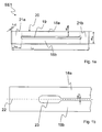
- Fig. 1a shows an inventive superconducting element SE1 with an elongated opening 19 in the form of a slot.
- the superconducting element SE1 comprises a central section 20, which is adjacent to two end sections 21a , 21b (in fig. 1 a the boundary of the central section 20 to the end sections 21a, 21b is shown by a dashed line).
- the end sections 21a, 21b may have a length Lend of several widths W SE of the superconducting element SE1.
- the elongated opening 19 is positioned in the central section 20 of the superconducting element SE1.
- the ends of the elongated opening 19 are adjacent to the end sections 21a, 21b of the superconducting element SE1.
- the opening 19 divides the central section 20 into two HTS strips 18a, 18b.
- the end sections 21a, 21b connect the HTS strips 18a, 18b thereby forming a closed loop that surrounds the opening 19.
- the elongated opening 19 is oriented along a longitudinal axis 22 of the superconducting element SE1 and comprises a minimal width W op .
- the width of the opening 19 is increased in order to suppress concentration of stress in the end of the opening 19, thereby increasing mechanical stability and lifetime of the superconducting element SE1.
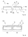
- FIG. 2a A cross sectional view of a partially prepared coated tape 27 is shown in fig. 2a and of an inventive superconducting element SE1 in fig. 2 b.
- a buffer layer 11 (which may comprise several buffer sub-layers) is deposited.
- a HTS layer 12 is deposited.
- a first metallic protection layer 14 is deposited on top of the HTS layer 12.
- the buffer layer 11 and the HTS layer 12 are deposited onto the top surface 24 of the substrate 10 and the buffer layer respectively, the first protection layer 14 also covers outer edge surfaces 25a, 25b (of the substrate 10 with deposited buffer layer 11 and HTS-layer 12).
- the first protection layer 14 may also cover the bottom side 26 of the substrate 10 in order to provide better stability and longer lifetime of the superconducting element SE1 (not shown).
- the thickness of the protection layer 14 may be inhomogeneous, especially in the vicinity of the outer edge surfaces 25a, 25b.
- Each layer 11, 12, 14 may be smoothed in the vicinity of the outer edge surfaces 25a, 25b, which is shown for the HTS-layer 12 and the protection layer 14 in fig. 2a . Thereby mechanical and electrical peculiarities can be suppressed at the corners of cross-section. Further time stability is improved.
- Fig. 2b shows that a second protection layer 15 is deposited from every side ("around") onto the (here two) HTS-strips 18a, 18b of the partially prepared coated tape 27, including outer edge surfaces 25a, 25b, inner edge surfaces 28a, 28b , top surface and bottom surface of the HTS-strips 18a, 18b of the partially prepared coated tape 27.
- the second protection layer 15 completely covers (envelops) the HTS-strips 18a, 18b in contrast to the first protection layer 14 which does not cover the inner surfaces 28a, 28b of the elongated opening 19 and the bottom surface 26 of the substrate 10.
- a basic conductive layer 16 is deposited, also completely covering the HTS-strips 18a, 18b from every side.
- the second protection layer 15 and the basic conductive layer 16 form a shunt layer 17.
- Fig. 3a, 3b show the partially prepared coated tape 27 (dashed line) which is enveloped by the shunt layer 17.
- the thicknesses of the second protection layer 15 and of the basic conductive layer 16 may be inhomogeneous, especially in the outer edge surfaces 25a, 25b of the superconducting element SE1 and in the edge surfaces 28a, 28b of the elongated opening 19.
- Fig. 4a, 4b show an inventive superconducting element SE2 with deformed HTS-strips 18a, 18b.
- the HTS strips 18a, 18b are deformed such that they are out of plane 34, which is defined by the end sections 21a, 21b of the superconducting element SE2.
- the HTS strips 18a, 18b may be kept deformed temporarily for deposition of the shunt layer 17 onto the inner edge surfaces 28a, 28b and then may be returned back to a flat form, as shown in fig. 1a . Please not that, due to clarity, the first protection layer is not shown in Fig. 4a .
- the HTS strips 18a, 18b deformed permanently. This may be important when the substrate tape width is small (say 4mm).
- the substrate width is small if it does not exceed the width of the elongated opening by a factor from 20 to 200. In this case, in order not to loose current the cutting prior to deposition of the shunt layer 17 is made very thin (50 ⁇ m for example).
- thickness of the basic conductive layer 16 e.g. Cu layer via galvanic plating
- the thickness of the shunt layer material deposited on the two inner edge surfaces 28a, 28b exceeds the width W op of the opening.
- An opening 19 that is smaller than the sum of the thicknesses of the shunt layer material deposited on the two inner edge surfaces 28a, 28b is called “narrow opening.”
- narrow opening it is advantageous to keep the HTS-strips 18a, 18b deformed permanently.
- the HTS-strips 18a, 18b are bent in different directions such that the plane 34 defined by the end sections 21a, 21b separates the HTS strips 18a, 18b, as shown in fig. 4b .
- Fig. 5a shows an inventive superconducting element SE3 with two openings 19a, 19b.
- the openings 19a, 19b divide the central section 20 of the superconducting element SE3 into three HTS-strips 18a, 18b, 18c.
- Superconducting elements SE3 with two openings can be used in order to provide a persistent coil consisting of two complimentary coils each of which corresponds to Fig. 5c .
- Fig. 5b shows a crossectional view of the superconducting element SE3 shown in fig.5a .
- the openings 19a, 19b of the superconducting element SE3 shown in fig. 5b are wider than the thickness of the of the shunt layer material deposited on the inner edge surfaces 28a, 28b.
- the HTS-strips 18a, 18b, 18c may either be returned to a flat form after deposition of the shunt layer 17 as shown in fig. 5b or can be kept deformed as shown for a superconducting element SE4 in fig. 5c .
- Fig. 6a, 6b show one end section 21 a of an inventive superconducting element SE5 which is provided with a protector.
- both end sections 21a, 21b are provided with protectors.
- the protector comprises an outer protection device 29 which covers at least the bottom and the top surface of the end section 21a of the superconducting element SE5.
- the outer protection device 29 may be a clamp with legs 30a, 30b (U-shaped) for inserting the end section 21a between the legs 30a, 30b of the U shaped clamp. It is also possible to provide separate outer protection elements for the bottom surface and the top surface of the end section 21a, which are fixed to the end section 21a.
- the outer protection device 29 is formed as a sleeve, thereby surrounding the whole end section 21a, including the outer side surfaces of the end sections. As shown in fig. 6b the outer protection device 29 protrudes over the end sections with protrusions 31a, 31b.
- the inventive protector may further comprise a spacer 32, which is placed between the deformed HTS-strips 18a, 18b, thereby sustaining the deformation of the HTS-strips 18a, 18b.
- Fig. 6b shows the spacer 32 which is positioned below HTS-strip 18a and above HTS-strip 18b thereby preventing the HTS-strips 18a, 18b from returning into the flat form and (in case of a narrow opening) from contacting each other.
- the spacer 32 can be attached to the outer protection device 29 via mechanical connecting elements 33a, 33b, as shown in fig. 6a .
- All embodiments of the inventive superconducting element comprise an opening which divides a central section into several HTS-strips, thereby defining a closed current loop within the superconducting element.
- the opening is the result of a cutting process which is carried out prior to the deposition of the shunt layer.
- the inventive superconducting element can achieve higher critical currents compared to known superconducting elements.
- the inventive shunt layer covers all surfaces of the HTS-strips, including the edge surfaces of the opening that resulted from the cutting process, thereby enhancing lifetime and operational stability of the superconducting element.
Description
- The invention relates to a superconducting element with a central section located between two end sections of the superconducting element, the superconducting element comprising: a substrate tape, a buffer layer, a high temperature superconducting (HTS) layer, a first protection layer, and a shunt layer, the superconducting element comprising at least one elongated opening in the central section, the opening being elongated between the two end sections, whereby the at least one elongated opening divides the central section of the superconducting element into at least two HTS strips.
- A layered HTS structure, comprising a substrate, a buffer layer, an HTS layer, a capping layer and a stabilizer layer, or a corresponding method for its manufacturing, respectively, is known from
US 7,774,035 B2 and "SuperPower 2G HTS Wire Specifications" 31. August 2009, pages 1-4. - A superconducting element with an elongated opening dividing a central section of the superconducting element into at least two HTS strips is known from
WO 2007/004787 A2 and Kosa et al. "Fault current limiter with novel arrangement of perfect YBCO loops made of HTS wire" 14th International power electronic and motion control conference (EPE/PEMC 2010), pages T10/69-73. - The invention deals with high temperature superconducting coated tapes and may be employed, in particular, in the fields of building of magnets, rotating machines machines and devices for energy storage, energy transmission, and energy distribution.
- Superconductors are used when large electric currents shall be transported or applied with low ohmic losses. High temperature superconductors, having a critical temperature high enough such that cooling may be done with liquid nitrogen (boiling point at atmospheric pressure about 77K), are inexpensive in cooling. However, due to their thin film nature combined with their ceramic properties, HTS conductors and elements are usually manufactured on substrates (HTS coated conductors); in particular, there are tape type substrates that typically offer some mechanical flexibility to HTS coated conductors. For HTS coated tapes, it is known to deposit the HTS film on a buffer layer deposited on the substrate, in order to achieve a beneficial HTS grain orientation needed for high critical currents. The HTS film is typically covered by a protection layer (also called capping layer) of a noble metal in order to avoid chemical reaction with aggressive environmental compositions (as e.g. acids, salt water, ...), and a shunt layer (also called stabilization layer) is deposited on top. The shunt layer shall ensure protection against high current overloads (electrical stabilization), e.g. in case of a quench.
- In applications, the HTS coated conductors are usually electrically connected one to other in order to provide a functional device or element to be employed in e.g. magnet, cable, motor, fault current limiter.
-
WO 2007/004787 A2 discloses a continuous closed superconducting loop with-out joint thereby reducing current loss. -
US 2007/0197395 A1 discloses a method for producing a superconducting element in which a substrate tape is coated with a metaloxy fluoride layer which is processed into a superconductor film. A protective layer is applied to the superconductor film. The tape is slit into HTS-wires. To improve mechanical robustness the resulting tapes are laminated with a stabilizing layer. - However, the time stability of superconducting elements being composed or formed from HTS coated tapes is not sufficient enough which is due to reduction of critical current and deterioration of mechanical parameters, e.g. of critical bending radius. Especially this is valid in superconducting elements that under-go electrical quench or are exploited in conditions where minimization of Joule's losses are important.
- It is an object of the invention to provide a superconductive element with improved electrical stabilization and time stability and a method for manufacturing such a superconducting element. Further object is to suppress Joule's losses in the superconducting element.
- This object is achieved, in accordance with the invention, by a superconducting element according to claim 1 and a method according to
claim 16. - According to the invention the shunt layer envelops the surface of each of the HTS strips.
- The opening defines a current path through the metallic substrate, in particular the path for fault current that appears when the HTS film is quenched under current that exceeds a critical threshold. Thereby less chemical diffusion is activated by both current transport and a bit higher temperature. In ac case the opening results in additional reduction of loss due to less width of particular parts of the superconducting element. Thus by providing the inventive elongated opening time stability of the superconducting element can be improved. An additional advantage is the equalization of currents. They become not dependent on transient resistances. Especially in case when a circular (eddy) current is generated within the superconducting element, the opening leads to reduction of Joule's losses (dc and ac).
- The opening can be produced by a cutting process.
- The two end sections join the HTS strips, thereby forming a "uninterrupted" superconducting electrical circuit with low Joule's losses. The elongated opening may be a slot with width in the range of 1-500µm, preferably 30-100µm. In a partially prepared state of the superconducting element (coated substrate without shunt layer) the opening exposes inner edge surfaces of the layered structure of the partially prepared coated tape, which face each other. Said inner edge surfaces will be referred to as "edge surfaces of the opening".
- The shunt layer is conductive, preferably metallic, and envelops the surface of each of the HTS strips, i.e. the shunt layer covers the whole surface of the HTS strips including the bottom surface and the top surface of the HTS strip as well as the edge surfaces of the opening.
- The inventive enveloping shunt layer provides a considerably more effective electrical stabilization (higher threshold of deterioration) compared to the known superconducting element, especially in case of an electrical quench, since the inventive shunt layer provides electrical stabilization in two directions: (i) along the elongation of the HTS strips and (ii) in perpendicular direction (along the circumference of the HTS strips), i.e. for "circumferential" currents.
- Further the inventive shunt layer effects better "encapsulation" of the HTS layer and buffer layer. I.e. the shunt layer protects the superconducting element against penetration of coolant (LHe2) or water or other liquids or vapors that may cause deterioration of the superconducting element. Therewith longer lifetime and better operational stability can be realized.
- For reasons of lower costs the substrate is preferably metallic, in particular it can be made of Cr-Ni stainless steel, typically sheeted to a width in the mm range or sub-mm range (preferably 2 mm - 100 mm), thus offering some mechanical flexibility. The tape is, in general, much longer than wide (typically by a factor of at least 10; note that the production may be based on "endless" tape), and much wider than thick (typically by a factor of at least 10).
- The shunt layer of the superconducting element according to the invention comprises a basic conductive layer and a second protection layer, whereby the second protection layer is provided between the first protection layer and the basic conductive layer. The second protection layer is preferably metallic. By providing a second protection layer, the superconducting element comprises a protection layer which is deposited in two steps (deposition of the first protection layer and deposition of the second protection layer, together forming the protection layer), whereby the cutting (e.g. laser beam cutting) is performed between the deposition of the first and the second protection layer. By this procedure, the HTS layer (which is deposited below the first protection layer) is already protected against reactive environment by the first protection layer when the cutting is started (which typically comes along with aggressive/reactive environment for the entire partially prepared coated tape). In turn, the "fresh" edges resulting from the cutting process (edge surfaces of the opening) will still be protected by the second protection layer deposited after the cutting and prior to the deposition of the basic conductive layer of the shunt layer. The deposition of the second conductive layer is advantageous if the materials of the substrate tape and the basic conductive layer only poorly adhere to each other (e.g. a Cu basic conductive layer and a stainless steel substrate). For very special combination of materials and deposition method for the shunt layer, the second protection layer may be omitted (i.e. the shunt layer only consists of the basic conductive layer), which is, however, outside the scope of the claims. Yet, the two-layered structure of the shunt layer causes better electrical performance (higher critical currents) and better time stability of the superconducting element being in direct contact with a liquid or gaseous coolant.
- The basic conductive layer is typically made of a non-noble metal, in particular copper, nickel or their alloys, often containing impurities, both of which may be reactive; in some cases basic conductive layers made of noble matalls, e.g. silver or gold, or the like may be used. The deposition of the basic conductive layer may comprise galvanic plating. This process is particularly simple and allows full coverage of the partially prepared coated tape without further measures.
- The superconducting element is preferably elongated. The elongated opening is advantageously provided in a longitudinal direction of the elongated superconducting element, i.e. the opening is elongated along the longer axis of superconducting element. This is advantageous e.g. for low voltage iSFCL (inductive superconducting fault current limiter with operating voltage of 10-20kV). Yet, for special applications, e.g. in iSFCL used for >100kV, it is also possible to orient the elongated opening in a transversal direction of the elongated superconducting element, i.e. the opening is elongated along the shorter axis of superconducting element. In case of a rectangular superconducting element the shorter axis is perpendicular to the longer axis.
- In order to suppress concentration of stress at the end of the opening the width of the elongated opening is preferably increased in a dilated area near to the end sections of the superconducting element. Thereby mechanical stability and lifetime of the superconducting element can be increased.
- In a preferred embodiment of the inventive superconducting element the length of the end section in longitudinal direction of the elongated opening exceeds the minimal width of each of the at least two HTS strips, in particular the length of the end sections exceeds the widths of the superconducting element. The longitudinal direction is the direction parallel to the major extension of the opening. The term "minimal width of the HTS-strip" does not include the width near the dilated area of the opening.
- By providing a length of the end sections that exceeds the width of the HTS strips a sufficient length of the end sections is ensured which allows to equalize superconducting currents when they flow in the same direction in different strips or to reduce Joule's losses in the areas of reversion of the current where self field becomes much more stronger. Moreover, sufficient length of the end section allows potentially jointing of several superconducting elements by connecting the end section of a first superconducting element to the end section of a second superconducting element in a persistent manner.
- Further preferred is an embodiment in which a ratio R of a thickness Tsub of the substrate and a width Wop of the elongated opening is in the range of R=0.5 to R=80. In this parameter range of R=Tsub/Wop, the critical current losses upon cutting have been found to be particularly low.
- The second protection layer advantageously covers at least partially the first protection layer and the edge surfaces (edge surfaces of the opening as well as outer edge surfaces if not covered by the first protection layer) of the underlying layers. By covering the edge surfaces of the underlying layers the penetration of aggressive chemicals (acids, water, ...) into the superconducting element structure can be avoided.
- In order to provide better stability and longer lifetime of the inventive superconducting element the second protection layer taken together with the first protection layer preferably envelops all surfaces of the superconducting element which is available before deposition of the basic conductive layer. I.e. the entity of the first and the second protection layer surrounds the partially prepared coated tape, including the substrate tape with buffer layer and HTS layer).
- The second protection layer (as well as the first protection layer) preferably comprises noble metals, copper or their alloys. It can be deposited via vacuum deposition. This grants a high quality deposition, in particular low in impurities. The thickness of the protection layer is preferably from 0.03 to 2 µm.
- In an advantageous embodiment the buffer layer comprises at least two different sub-layers, thereby providing an improved template for HTS layer growth and/or a diffusion barrier. Further mismatch in crystalline lattice parameters can be compensated. The sub-layers are preferably dielectric. The first sub-layer is preferably made of materials with a chemical barrier, the capability to serve as a crystalline template and a moderate mismatch of lattice parameters with the HTS layer. It may be based on yttria stabilized zirconia (YSZ ) (with a preferred thickness of 0.3-3µm , in particular ca. 1.5 µm) which is bi-axially textured via alternating beam assisted deposition (ABAD) (compare
EP 1 693 905 B1 for details), and a so called cap layer may comprise CeO2 (second sub-layer) with a preferred thickness of 0.01 to 1µm, in particular about 0.1 µm. ABAD produces a textured template for appropriate growth of the HTS layer. It is also possible to deposit a planarization sub-layer made of aluminia (Al2O3) prior to YSZ and CeO2 sub-layers. Other suitable first sub-layer materials are e.g. MgO, gadolinium zirconate, titan nitride, cerium oxide. The cap layer can also be made of barium zirconate and plenty of other materials which show a small mismatch of lattice parameters with the HTS layer. - The HTS-layer preferably comprises a high temperature superconductor as ReBa2Cu3O7-x or their mixtures, where Re denotes a rare earth element. The HTS layer (HTS-film) is preferably based on YBa2Cu3O7-x, with a preferred thickness of 0.1 to 10µm, in particular about 1.5µm . The second buffer sub-layer and the HTS layer are preferably processed via pulsed laser deposition.
- In a highly preferred embodiment the end sections comprise a protector for limiting bending and torsion of the at least two strips. Thereby bending and torsion of the superconducting element can be limited in the range which avoids deterioration of a critical current in the at least two HTS strips. The protector is typically made of a non-magnetic metall, preferably Cu, stainless steel, or silver. The protector can be fixed to the superconducting element (preferably in the very end of the superconducting element) via mechanical coupling (as e.g. clamping) with edge areas of the strips or via glue bonding. Alternatively, the end sections of the superconducting element can be simply inserted in the protector.
- The protector preferably projects above the end sections of the superconducting element in their longitudinal direction.
- In a special embodiment of the inventive superconducting element the HTS-strips are mechanically deformed, in particular twisted and/or bent. This is advantageous when the initial tape width is small (say 4mm). In this case the cutting before deposition of the shunt layer is made very thin, 50µm for example, in order not to loose current. On the other hand the thickness of the basic conductive layer may be equal to 50µm or even more. By deforming the HTS strips a non-flat superconducting element can be formed and mechanical contact between the HTS-strips can be prevented.
- The invention also concerns a superconducting coil which comprises an inventive superconducting element.
- Further the invention concerns a method for manufacturing the inventive superconducting element, the method comprising the following steps:
- a providing a substrate tape,
- b depositing a buffer layer onto the substrate tape,
- c depositing a HTS layer onto the buffer layer,
- d depositing a first protection layer onto the HTS layer and
- e depositing a shunt layer.
- The substrate tape which is at least coated with a buffer sub-layer, but is not coated with a shunt layer is referred to as a "partially prepared coated tape". According to the invention a cutting of the partially prepared coated tape is performed prior to the deposition of the shunt layer thereby dividing a central part of the partially prepared coated tape into at least two HTS-strips. Thereby spreading of damages from the immediate cutting zone during cutting can be reduced. The shunt layer is deposited onto all surfaces of each of the HTS-strips of the partially prepared coated tape. Thus an inventive superconducting element can be produced.
- The cutting is preferably performed by laser beam cutting which is applied together with a gas flow and/or a liquid flow directed along the laser beam. Yet, it is also possible to perform a water-jet cutting or an electron-beam cutting.
- The cutting may be performed prior to deposition of the second protection layer, preferably after deposition of the
first protection layer 14. Cutting can also be carried out in an earlier stage of production, as long as the deposition of at least one sub-layer of thebuffer layer 11 has been carried out. - Advantageously the HTS strips are tilted relative to each other or defomed during deposition of the shunt layer, thereby keeping the partially prepared coated tape in a non-flat form.
- Further advantages can be extracted from the description and the enclosed drawing. The features mentioned above and below can be used in accordance with the invention either individually or collectively in any combination. The embodiments mentioned are not to be understood as exhaustive enumeration but rather have exemplary character for the description of the invention.
- The invention is shown in the drawing.
- Fig. 1a
- shows schematically an inventive superconducting element with an elongated opening.
- Fig. 1 b
- shows schematically a detailed partial view of the superconducting element shown in
fig. 1 b. - Fig. 2
- shows schematically a transversal crossectional view of an inventive superconducting element, exposing the layer sequence.
- Fig. 3a
- shows schematically an inventive superconducting element with shunt layer enveloping a partially prepared HTS coated tape.
- Fig. 3b
- shows schematically a side view of the superconducting element shown in
fig. 3a . - Fig. 4a
- shows schematically a transversal crossectional view in plane A-A of an inventive superconducting element with narrow opening and deformed HTS-strips.
- Fig. 4b
- shows schematically a side view of the superconducting element shown in
fig.4a . - Fig. 5a
- shows schematically a top view of an inventive superconducting element with two openings.
- Fig. 5b
- shows schematically a transversal crossectional view of the superconducting element shown in
fig.5a . - Fig. 5c
- shows schematically an inventive superconducting element with two openings and deformed HTS-strips.
- Fig. 6a
- shows schematically a partial top view of an inventive superconducting element provided with protectors.
- Fig. 6b
- shows schematically a side view of the superconducting element shown in
fig.6a . -
Fig. 1a shows an inventive superconducting element SE1 with anelongated opening 19 in the form of a slot. The superconducting element SE1 comprises acentral section 20, which is adjacent to twoend sections fig. 1 a the boundary of thecentral section 20 to theend sections end sections elongated opening 19 is positioned in thecentral section 20 of the superconducting element SE1. The ends of theelongated opening 19 are adjacent to theend sections opening 19 divides thecentral section 20 into twoHTS strips end sections opening 19. - As shown in
fig. 1b theelongated opening 19 is oriented along alongitudinal axis 22 of the superconducting element SE1 and comprises a minimal width Wop. In dilatedareas 23 at both ends of theopening 19, the width of theopening 19 is increased in order to suppress concentration of stress in the end of theopening 19, thereby increasing mechanical stability and lifetime of the superconducting element SE1. - A cross sectional view of a partially prepared coated
tape 27 is shown infig. 2a and of an inventive superconducting element SE1 infig. 2 b. - On a
substrate tape 10, a buffer layer 11 (which may comprise several buffer sub-layers) is deposited. On top of thebuffer layer 11, aHTS layer 12 is deposited. Further, a firstmetallic protection layer 14 is deposited on top of theHTS layer 12. Whereas thebuffer layer 11 and theHTS layer 12 are deposited onto thetop surface 24 of thesubstrate 10 and the buffer layer respectively, thefirst protection layer 14 also coversouter edge surfaces substrate 10 with depositedbuffer layer 11 and HTS-layer 12). Thus, penetration of aggressive chemicals (acids, water ...) into the superconducting element structure can be prevented. Thefirst protection layer 14 may also cover thebottom side 26 of thesubstrate 10 in order to provide better stability and longer lifetime of the superconducting element SE1 (not shown). - The thickness of the
protection layer 14 may be inhomogeneous, especially in the vicinity of theouter edge surfaces layer outer edge surfaces layer 12 and theprotection layer 14 infig. 2a . Thereby mechanical and electrical peculiarities can be suppressed at the corners of cross-section. Further time stability is improved. - The
opening 19, which isprovided by a cutting process, extends through the substrate and all deposited layers (11, 12, 14) of the partially prepared coatedtape 27, thereby exposinginner edge surfaces opening 19. -
Fig. 2b shows that asecond protection layer 15 is deposited from every side ("around") onto the (here two) HTS-strips tape 27, includingouter edge surfaces inner edge surfaces strips tape 27. As a result, thesecond protection layer 15 completely covers (envelops) the HTS-strips first protection layer 14 which does not cover theinner surfaces elongated opening 19 and thebottom surface 26 of thesubstrate 10. Subsequently, a basicconductive layer 16 is deposited, also completely covering the HTS-strips second protection layer 15 and the basicconductive layer 16 form ashunt layer 17. -
Fig. 3a, 3b show the partially prepared coated tape 27 (dashed line) which is enveloped by theshunt layer 17. - The thicknesses of the
second protection layer 15 and of the basicconductive layer 16 may be inhomogeneous, especially in theouter edge surfaces elongated opening 19. -
Fig. 4a, 4b show an inventive superconducting element SE2 with deformed HTS-strips plane 34, which is defined by theend sections shunt layer 17 onto theinner edge surfaces fig. 1a . Please not that, due to clarity, the first protection layer is not shown inFig. 4a . - In certain circumstances it is preferred to keep the HTS strips 18a, 18b deformed permanently. This may be important when the substrate tape width is small (say 4mm). The substrate width is small if it does not exceed the width of the elongated opening by a factor from 20 to 200. In this case, in order not to loose current the cutting prior to deposition of the
shunt layer 17 is made very thin (50µm for example). On the other hand thickness of the basic conductive layer 16 (e.g. Cu layer via galvanic plating) may be equal to 50µm or even more. Thus the thickness of the shunt layer material deposited on the twoinner edge surfaces opening 19 that is smaller than the sum of the thicknesses of the shunt layer material deposited on the twoinner edge surfaces strips strips plane 34 defined by theend sections fig. 4b . -
Fig. 5a shows an inventive superconducting element SE3 with twoopenings openings central section 20 of the superconducting element SE3 into three HTS-strips Fig. 5c . - This may used not only in magnets but also in iSFCLs
-
Fig. 5b shows a crossectional view of the superconducting element SE3 shown infig.5a . In contrast to the superconducting element SE2 shown infig. 4a theopenings fig. 5b are wider than the thickness of the of the shunt layer material deposited on theinner edge surfaces strips shunt layer 17 as shown infig. 5b or can be kept deformed as shown for a superconducting element SE4 infig. 5c . -
Fig. 6a, 6b show oneend section 21 a of an inventive superconducting element SE5 which is provided with a protector. In general, bothend sections - The protector comprises an
outer protection device 29 which covers at least the bottom and the top surface of theend section 21a of the superconducting element SE5. Theouter protection device 29 may be a clamp withlegs end section 21a between thelegs end section 21a, which are fixed to theend section 21a. Preferably theouter protection device 29 is formed as a sleeve, thereby surrounding thewhole end section 21a, including the outer side surfaces of the end sections. As shown infig. 6b theouter protection device 29 protrudes over the end sections withprotrusions - The inventive protector may further comprise a
spacer 32, which is placed between the deformed HTS-strips strips Fig. 6b shows thespacer 32 which is positioned below HTS-strip 18a and above HTS-strip 18b thereby preventing the HTS-strips spacer 32 can be attached to theouter protection device 29 via mechanical connectingelements fig. 6a . - All embodiments of the inventive superconducting element comprise an opening which divides a central section into several HTS-strips, thereby defining a closed current loop within the superconducting element. The opening is the result of a cutting process which is carried out prior to the deposition of the shunt layer. Thus the shunt layer cannot be damaged during the cutting process. The inventive superconducting element can achieve higher critical currents compared to known superconducting elements. The inventive shunt layer covers all surfaces of the HTS-strips, including the edge surfaces of the opening that resulted from the cutting process, thereby enhancing lifetime and operational stability of the superconducting element.
- List of reference signs
- 10
- su bstrate
- 11
- buffer layer
- 12
- HTS layer
- 14
- first protection layer
- 15
- second protection layer
- 16
- basic conductive layer
- 17
- shunt layer
- 18a, 18b, 18c
- HTS strips
- 19
- opening
- 20
- central section
- 21a, 21b
- end sections
- 22
- longitudinal axis of superconducting element (longer axis)
- 23
- dilated area
- 24
- top surface
- 25a, 25b
- outer edge surfaces of the partially prepared coated tape
- 26
- bottom surface of the substrate
- 27
- partially prepared coated tape
- 28a, 28b
- inner edge surfaces of the partially prepared coated tape = edge surfaces of the opening
- 29
- outer projection device
- 30a. 30b
- legs
- 31 a, 31 b.
- protrusion of the outer projection device
- 32
- spacer
- 33a, 33b
- connecting elements
- 34
- plane defined by end sections
- Lend
- length of the end section
- LSE
- length of the superconducting element
- SE, SE'
- superconducting element
- Tsub
- thickness of substrate
- Wop
- width of the opening
- WSE
- width of the superconducting element
- Wstrip
- width of the HTS-strip
Claims (17)
- Superconducting element (SE1, SE2, SE3, SE4, SE5) with a central section (20) located between two end sections (21 a, 21 b) of the superconducting element (SE1, SE2, SE3, SE4, SE5), the superconducting element (SE1, SE2, SE3, SE4, SE5) comprising:a substrate tape (10),a buffer layer (11),a high temperature superconducting (HTS) layer (12),a first protection layer (14), anda shunt layer (17),the superconducting element (SE1, SE2, SE3, SE4, SE5) further comprising at least one elongated opening (19) in the central section (20) elongated between the two end sections (21 a, 21 b),whereby the at least one elongated opening (19) divides the central section (20) of the superconducting element (SE1, SE2, SE3, SE4, SE5) into at least two HTS strips (18a, 18b, 18c),characterized in
that the shunt layer (17) envelops the surface of each of the HTS strips (18a, 18b, 18c), and
that the shunt layer (17) comprises a basic conductive layer (16) and a second protection layer (15), whereby the second protection layer (15) is provided between the first protection layer (14) and the basic conductive layer (16). - Superconducting element (SE1, SE2, SE3, SE4, SE5) according to claim 1, characterized in that the superconducting element (SE1, SE2, SE3, SE4, SE5) is elongated.
- Superconducting element (SE1, SE2, SE3, SE4, SE5) according to one of the preceding claims, characterized in that near to the end sections (21 a, 21 b) of the superconducting element (SE1, SE2, SE3, SE4, SE5) the width (Wop) of the elongated opening (19) is increased in a dilated area (23).
- Superconducting element (SE1, SE2, SE5) according to one of the preceding claims, characterized in that the length (Lend) of the end section (21 a, 21 b) in longitudinal direction of the elongated opening (19) exceeds the minimal width (Wstrip) of each of the at least two strips (18a, 18b, 18c), in particular exceeds the width (WSE) of the superconducting element (SE1, SE2, SE5).
- Superconducting element (SE1, SE2, SE3, SE4, SE5) according to one of the preceding claims, characterized in that a ratio R of a thickness (Tsub) of the substrate (10) and a width (Wop) of the elongated opening (19) is in the range of R=0.5 to R=80.
- Superconducting element (SE1, SE2, SE3, SE4, SE5) according to one of the preceding claims, characterized in that the second protection layer (15) covers at least partially the first protection layer (14) and edge surfaces (25a, 25b, 28a, 28b) of the underlying layers (11, 12, 14).
- Superconducting element (SE1, SE2, SE3, SE4, SE5) according to one of the preceding claims, characterized in that the second protection layer (15) taken together with the first protection layer (14) envelops all surfaces of the superconducting element (SE1, SE2, SE3, SE4, SE5) which is available before deposition of the basic conductive layer (16).
- Superconducting element (SE1, SE2, SE3, SE4, SE5) according to one of the preceding claims, characterized in that the second protection layer (15) comprises noble metals, copper or their alloys.
- Superconducting element (SE1, SE2, SE3, SE4, SE5) according to one of the preceding claims, characterized in that the basic conductive layer (16) comprises noble metals, copper, nickel or their alloys.
- Superconducting element (SE1, SE2, SE3, SE4, SE5) according to one of the preceding claims, characterized in the buffer layer (11) comprises at least two different sub-layers.
- Superconducting element (SE1, SE2, SE3, SE4, SE5) according to one of the preceding claims, characterized in that the HTS layer (12) comprises a high temperature superconductor as ReBa2Cu3O7-x or their mixtures, where Re denotes a rare earth element.
- Superconducting element (SE5) according to one of the preceding claims, characterized in that the end sections (21 a, 21 b) comprise a protector for limiting bending and torsion of the at least two strips (18a, 18b, 18c).
- Superconducting element (SE1, SE2, SE3, SE4, SE5) according to claim 12, characterized in that the protector projects above the end sections (21 a, 21 b) in their longitudinal direction.
- Superconducting element (SE2, SE4, SE5) according to one of the preceding claims, characterized in that the HTS strips (18a, 18b, 18c) are mechanically deformed, in particular twisted and/or bent.
- Superconducting coil characterized in that it comprises a superconducting element (SE1, SE2, SE3, SE4, SE5) according to one of the preceding claims.
- Method for manufacturing a high temperature superconducting element (SE1, SE2, SE3, SE4, SE5) with the following steps:a. providing a substrate tape (10),b. depositing a buffer layer (11) onto the substrate tape (10),c. depositing a HTS layer (12) onto the buffer layer (11),d. depositing a first protection layer (13) onto the HTS layer (12) ande. depositing a shunt layer (17)characterized in
that prior to the deposition of the shunt layer (17) a cutting of the partially prepared coated tape (27) is performed thereby dividing a central part (20) of the partially prepared coated tape into at least two HTS strips (18a, 18b, 18c), and
that the shunt layer (17) is deposited onto all surfaces of each of the HTS strips (18a, 18b, 18c) of the partially prepared coated tape (27), whereby the shunt layer (17) comprises a basic conductive layer (16) and a second protection layer (15), whereby the second protection layer (15) is provided between the first protection layer (14) and the basic conductive layer (16). - Method according to claim 16, characterized in that during deposition of the shunt layer (17) the HTS strips (18a, 18b, 18c) are tilted relative to each other, thereby keeping the partially prepared coated tape (27) in a non-flat form.
Priority Applications (2)
| Application Number | Priority Date | Filing Date | Title |
|---|---|---|---|
| EP11154949.9A EP2490272B1 (en) | 2011-02-18 | 2011-02-18 | Superconducting element with elongated opening and method for manufacturing the same |
| US13/396,612 US8802598B2 (en) | 2011-02-18 | 2012-02-15 | Superconducting element with elongated opening and method for manufacturing a superconducting element |
Applications Claiming Priority (1)
| Application Number | Priority Date | Filing Date | Title |
|---|---|---|---|
| EP11154949.9A EP2490272B1 (en) | 2011-02-18 | 2011-02-18 | Superconducting element with elongated opening and method for manufacturing the same |
Publications (2)
| Publication Number | Publication Date |
|---|---|
| EP2490272A1 EP2490272A1 (en) | 2012-08-22 |
| EP2490272B1 true EP2490272B1 (en) | 2013-08-21 |
Family
ID=44317910
Family Applications (1)
| Application Number | Title | Priority Date | Filing Date |
|---|---|---|---|
| EP11154949.9A Not-in-force EP2490272B1 (en) | 2011-02-18 | 2011-02-18 | Superconducting element with elongated opening and method for manufacturing the same |
Country Status (2)
| Country | Link |
|---|---|
| US (1) | US8802598B2 (en) |
| EP (1) | EP2490272B1 (en) |
Families Citing this family (5)
| Publication number | Priority date | Publication date | Assignee | Title |
|---|---|---|---|---|
| EP2490273B1 (en) * | 2011-02-18 | 2013-05-01 | Bruker HTS GmbH | Method for manufacturing a HTS coated tape with laser beam cutting |
| WO2014104208A1 (en) * | 2012-12-28 | 2014-07-03 | 株式会社フジクラ | Oxide superconducting wire |
| KR101459583B1 (en) * | 2013-09-11 | 2014-11-10 | 주식회사 서남 | Superconductor and method for manufacturing the same |
| US9847588B2 (en) * | 2015-05-19 | 2017-12-19 | Varian Semiconductor Equipment Associates, Inc. | Connecting system for superconducting systems |
| CN106654501B (en) * | 2016-12-15 | 2019-04-23 | 电子科技大学 | Cavity resonator production method based on deformable high temperature superconducting materia |
Family Cites Families (5)
| Publication number | Priority date | Publication date | Assignee | Title |
|---|---|---|---|---|
| US7774035B2 (en) | 2003-06-27 | 2010-08-10 | Superpower, Inc. | Superconducting articles having dual sided structures |
| DE502005005097D1 (en) | 2005-02-17 | 2008-10-02 | Europ High Temperature Superco | Process for producing biaxially oriented thin films |
| KR100720057B1 (en) * | 2005-07-06 | 2007-05-18 | 학교법인 한국산업기술대학 | Superconduction Magnet And Manufacturing Method For Persistent Current |
| US7674751B2 (en) * | 2006-01-10 | 2010-03-09 | American Superconductor Corporation | Fabrication of sealed high temperature superconductor wires |
| KR100766052B1 (en) | 2006-11-10 | 2007-10-12 | 학교법인 한국산업기술대학 | Filament type coated superconductor and the method for fabricating the same |
-
2011
- 2011-02-18 EP EP11154949.9A patent/EP2490272B1/en not_active Not-in-force
-
2012
- 2012-02-15 US US13/396,612 patent/US8802598B2/en not_active Expired - Fee Related
Also Published As
| Publication number | Publication date |
|---|---|
| EP2490272A1 (en) | 2012-08-22 |
| US20120214673A1 (en) | 2012-08-23 |
| US8802598B2 (en) | 2014-08-12 |
Similar Documents
| Publication | Publication Date | Title |
|---|---|---|
| CA2772158C (en) | Multifilament conductor and method for its production | |
| EP2770513B1 (en) | Oxide superconductor wire and method of manufacturing oxide superconductor wire | |
| EP2490272B1 (en) | Superconducting element with elongated opening and method for manufacturing the same | |
| EP3133612B1 (en) | Oxide superconducting wire material and oxide superconducting wire material production method | |
| EP2490273B1 (en) | Method for manufacturing a HTS coated tape with laser beam cutting | |
| KR102562414B1 (en) | Superconducting wire and superconducting coil | |
| EP2958115B1 (en) | Oxide superconducting wire | |
| KR20110127634A (en) | Thin-film superconducting wire rod and superconducting cable conductor | |
| US20210184096A1 (en) | Fabrication of superconductor wire | |
| EP3367394A1 (en) | Oxide superconducting wire | |
| US20200343652A1 (en) | Joined superconducting tape | |
| US9640979B2 (en) | Band-shaped superconducting element with improved self-protection in case of quenching | |
| JP2005044636A (en) | Superconductive wire rod | |
| RU2719388C1 (en) | Superconducting wire and superconducting coil | |
| JP2018055990A (en) | Superconductive current lead and oxide superconducting wire material | |
| EP3696826A1 (en) | Connection structure for oxide superconducting wire materials | |
| JP6492205B2 (en) | Manufacturing method of oxide superconducting wire | |
| JP2017152210A (en) | Oxide superconducting wire and manufacturing method therefor | |
| WO2018216064A1 (en) | Superconducting wire material and superconducting coil | |
| CN117836874A (en) | Superconducting wire | |
| CN117882153A (en) | Superconducting wire and superconducting wire connection structure |
Legal Events
| Date | Code | Title | Description |
|---|---|---|---|
| PUAI | Public reference made under article 153(3) epc to a published international application that has entered the european phase |
Free format text: ORIGINAL CODE: 0009012 |
|
| 17P | Request for examination filed |
Effective date: 20111220 |
|
| AK | Designated contracting states |
Kind code of ref document: A1 Designated state(s): AL AT BE BG CH CY CZ DE DK EE ES FI FR GB GR HR HU IE IS IT LI LT LU LV MC MK MT NL NO PL PT RO RS SE SI SK SM TR |
|
| AX | Request for extension of the european patent |
Extension state: BA ME |
|
| GRAP | Despatch of communication of intention to grant a patent |
Free format text: ORIGINAL CODE: EPIDOSNIGR1 |
|
| GRAS | Grant fee paid |
Free format text: ORIGINAL CODE: EPIDOSNIGR3 |
|
| GRAA | (expected) grant |
Free format text: ORIGINAL CODE: 0009210 |
|
| AK | Designated contracting states |
Kind code of ref document: B1 Designated state(s): AL AT BE BG CH CY CZ DE DK EE ES FI FR GB GR HR HU IE IS IT LI LT LU LV MC MK MT NL NO PL PT RO RS SE SI SK SM TR |
|
| REG | Reference to a national code |
Ref country code: GB Ref legal event code: FG4D |
|
| REG | Reference to a national code |
Ref country code: CH Ref legal event code: EP |
|
| REG | Reference to a national code |
Ref country code: AT Ref legal event code: REF Ref document number: 628545 Country of ref document: AT Kind code of ref document: T Effective date: 20130915 |
|
| REG | Reference to a national code |
Ref country code: IE Ref legal event code: FG4D |
|
| REG | Reference to a national code |
Ref country code: DE Ref legal event code: R096 Ref document number: 602011002642 Country of ref document: DE Effective date: 20131017 |
|
| REG | Reference to a national code |
Ref country code: NL Ref legal event code: VDEP Effective date: 20130821 Ref country code: AT Ref legal event code: MK05 Ref document number: 628545 Country of ref document: AT Kind code of ref document: T Effective date: 20130821 |
|
| REG | Reference to a national code |
Ref country code: LT Ref legal event code: MG4D |
|
| PG25 | Lapsed in a contracting state [announced via postgrant information from national office to epo] |
Ref country code: IS Free format text: LAPSE BECAUSE OF FAILURE TO SUBMIT A TRANSLATION OF THE DESCRIPTION OR TO PAY THE FEE WITHIN THE PRESCRIBED TIME-LIMIT Effective date: 20131221 Ref country code: LT Free format text: LAPSE BECAUSE OF FAILURE TO SUBMIT A TRANSLATION OF THE DESCRIPTION OR TO PAY THE FEE WITHIN THE PRESCRIBED TIME-LIMIT Effective date: 20130821 Ref country code: AT Free format text: LAPSE BECAUSE OF FAILURE TO SUBMIT A TRANSLATION OF THE DESCRIPTION OR TO PAY THE FEE WITHIN THE PRESCRIBED TIME-LIMIT Effective date: 20130821 Ref country code: CY Free format text: LAPSE BECAUSE OF FAILURE TO SUBMIT A TRANSLATION OF THE DESCRIPTION OR TO PAY THE FEE WITHIN THE PRESCRIBED TIME-LIMIT Effective date: 20130911 Ref country code: PT Free format text: LAPSE BECAUSE OF FAILURE TO SUBMIT A TRANSLATION OF THE DESCRIPTION OR TO PAY THE FEE WITHIN THE PRESCRIBED TIME-LIMIT Effective date: 20131223 Ref country code: HR Free format text: LAPSE BECAUSE OF FAILURE TO SUBMIT A TRANSLATION OF THE DESCRIPTION OR TO PAY THE FEE WITHIN THE PRESCRIBED TIME-LIMIT Effective date: 20130821 Ref country code: NO Free format text: LAPSE BECAUSE OF FAILURE TO SUBMIT A TRANSLATION OF THE DESCRIPTION OR TO PAY THE FEE WITHIN THE PRESCRIBED TIME-LIMIT Effective date: 20131121 Ref country code: SE Free format text: LAPSE BECAUSE OF FAILURE TO SUBMIT A TRANSLATION OF THE DESCRIPTION OR TO PAY THE FEE WITHIN THE PRESCRIBED TIME-LIMIT Effective date: 20130821 |
|
| PG25 | Lapsed in a contracting state [announced via postgrant information from national office to epo] |
Ref country code: SI Free format text: LAPSE BECAUSE OF FAILURE TO SUBMIT A TRANSLATION OF THE DESCRIPTION OR TO PAY THE FEE WITHIN THE PRESCRIBED TIME-LIMIT Effective date: 20130821 Ref country code: LV Free format text: LAPSE BECAUSE OF FAILURE TO SUBMIT A TRANSLATION OF THE DESCRIPTION OR TO PAY THE FEE WITHIN THE PRESCRIBED TIME-LIMIT Effective date: 20130821 Ref country code: BE Free format text: LAPSE BECAUSE OF FAILURE TO SUBMIT A TRANSLATION OF THE DESCRIPTION OR TO PAY THE FEE WITHIN THE PRESCRIBED TIME-LIMIT Effective date: 20130821 Ref country code: GR Free format text: LAPSE BECAUSE OF FAILURE TO SUBMIT A TRANSLATION OF THE DESCRIPTION OR TO PAY THE FEE WITHIN THE PRESCRIBED TIME-LIMIT Effective date: 20131122 Ref country code: PL Free format text: LAPSE BECAUSE OF FAILURE TO SUBMIT A TRANSLATION OF THE DESCRIPTION OR TO PAY THE FEE WITHIN THE PRESCRIBED TIME-LIMIT Effective date: 20130821 Ref country code: FI Free format text: LAPSE BECAUSE OF FAILURE TO SUBMIT A TRANSLATION OF THE DESCRIPTION OR TO PAY THE FEE WITHIN THE PRESCRIBED TIME-LIMIT Effective date: 20130821 |
|
| PG25 | Lapsed in a contracting state [announced via postgrant information from national office to epo] |
Ref country code: CY Free format text: LAPSE BECAUSE OF FAILURE TO SUBMIT A TRANSLATION OF THE DESCRIPTION OR TO PAY THE FEE WITHIN THE PRESCRIBED TIME-LIMIT Effective date: 20130821 |
|
| PG25 | Lapsed in a contracting state [announced via postgrant information from national office to epo] |
Ref country code: CZ Free format text: LAPSE BECAUSE OF FAILURE TO SUBMIT A TRANSLATION OF THE DESCRIPTION OR TO PAY THE FEE WITHIN THE PRESCRIBED TIME-LIMIT Effective date: 20130821 Ref country code: RO Free format text: LAPSE BECAUSE OF FAILURE TO SUBMIT A TRANSLATION OF THE DESCRIPTION OR TO PAY THE FEE WITHIN THE PRESCRIBED TIME-LIMIT Effective date: 20130821 Ref country code: EE Free format text: LAPSE BECAUSE OF FAILURE TO SUBMIT A TRANSLATION OF THE DESCRIPTION OR TO PAY THE FEE WITHIN THE PRESCRIBED TIME-LIMIT Effective date: 20130821 Ref country code: SK Free format text: LAPSE BECAUSE OF FAILURE TO SUBMIT A TRANSLATION OF THE DESCRIPTION OR TO PAY THE FEE WITHIN THE PRESCRIBED TIME-LIMIT Effective date: 20130821 Ref country code: NL Free format text: LAPSE BECAUSE OF FAILURE TO SUBMIT A TRANSLATION OF THE DESCRIPTION OR TO PAY THE FEE WITHIN THE PRESCRIBED TIME-LIMIT Effective date: 20130821 Ref country code: DK Free format text: LAPSE BECAUSE OF FAILURE TO SUBMIT A TRANSLATION OF THE DESCRIPTION OR TO PAY THE FEE WITHIN THE PRESCRIBED TIME-LIMIT Effective date: 20130821 |
|
| PG25 | Lapsed in a contracting state [announced via postgrant information from national office to epo] |
Ref country code: IT Free format text: LAPSE BECAUSE OF FAILURE TO SUBMIT A TRANSLATION OF THE DESCRIPTION OR TO PAY THE FEE WITHIN THE PRESCRIBED TIME-LIMIT Effective date: 20130821 Ref country code: ES Free format text: LAPSE BECAUSE OF FAILURE TO SUBMIT A TRANSLATION OF THE DESCRIPTION OR TO PAY THE FEE WITHIN THE PRESCRIBED TIME-LIMIT Effective date: 20130821 |
|
| PLBE | No opposition filed within time limit |
Free format text: ORIGINAL CODE: 0009261 |
|
| STAA | Information on the status of an ep patent application or granted ep patent |
Free format text: STATUS: NO OPPOSITION FILED WITHIN TIME LIMIT |
|
| 26N | No opposition filed |
Effective date: 20140522 |
|
| REG | Reference to a national code |
Ref country code: DE Ref legal event code: R097 Ref document number: 602011002642 Country of ref document: DE Effective date: 20140522 |
|
| PG25 | Lapsed in a contracting state [announced via postgrant information from national office to epo] |
Ref country code: LU Free format text: LAPSE BECAUSE OF FAILURE TO SUBMIT A TRANSLATION OF THE DESCRIPTION OR TO PAY THE FEE WITHIN THE PRESCRIBED TIME-LIMIT Effective date: 20140218 Ref country code: MC Free format text: LAPSE BECAUSE OF FAILURE TO SUBMIT A TRANSLATION OF THE DESCRIPTION OR TO PAY THE FEE WITHIN THE PRESCRIBED TIME-LIMIT Effective date: 20130821 |
|
| REG | Reference to a national code |
Ref country code: IE Ref legal event code: MM4A |
|
| PG25 | Lapsed in a contracting state [announced via postgrant information from national office to epo] |
Ref country code: IE Free format text: LAPSE BECAUSE OF NON-PAYMENT OF DUE FEES Effective date: 20140218 |
|
| REG | Reference to a national code |
Ref country code: FR Ref legal event code: PLFP Year of fee payment: 6 |
|
| PG25 | Lapsed in a contracting state [announced via postgrant information from national office to epo] |
Ref country code: MT Free format text: LAPSE BECAUSE OF FAILURE TO SUBMIT A TRANSLATION OF THE DESCRIPTION OR TO PAY THE FEE WITHIN THE PRESCRIBED TIME-LIMIT Effective date: 20130821 |
|
| PG25 | Lapsed in a contracting state [announced via postgrant information from national office to epo] |
Ref country code: SM Free format text: LAPSE BECAUSE OF FAILURE TO SUBMIT A TRANSLATION OF THE DESCRIPTION OR TO PAY THE FEE WITHIN THE PRESCRIBED TIME-LIMIT Effective date: 20130821 |
|
| PG25 | Lapsed in a contracting state [announced via postgrant information from national office to epo] |
Ref country code: RS Free format text: LAPSE BECAUSE OF NON-PAYMENT OF DUE FEES Effective date: 20130821 Ref country code: BG Free format text: LAPSE BECAUSE OF FAILURE TO SUBMIT A TRANSLATION OF THE DESCRIPTION OR TO PAY THE FEE WITHIN THE PRESCRIBED TIME-LIMIT Effective date: 20130821 |
|
| PG25 | Lapsed in a contracting state [announced via postgrant information from national office to epo] |
Ref country code: TR Free format text: LAPSE BECAUSE OF FAILURE TO SUBMIT A TRANSLATION OF THE DESCRIPTION OR TO PAY THE FEE WITHIN THE PRESCRIBED TIME-LIMIT Effective date: 20130821 Ref country code: HU Free format text: LAPSE BECAUSE OF FAILURE TO SUBMIT A TRANSLATION OF THE DESCRIPTION OR TO PAY THE FEE WITHIN THE PRESCRIBED TIME-LIMIT; INVALID AB INITIO Effective date: 20110218 |
|
| REG | Reference to a national code |
Ref country code: FR Ref legal event code: PLFP Year of fee payment: 7 |
|
| REG | Reference to a national code |
Ref country code: FR Ref legal event code: PLFP Year of fee payment: 8 |
|
| PG25 | Lapsed in a contracting state [announced via postgrant information from national office to epo] |
Ref country code: MK Free format text: LAPSE BECAUSE OF FAILURE TO SUBMIT A TRANSLATION OF THE DESCRIPTION OR TO PAY THE FEE WITHIN THE PRESCRIBED TIME-LIMIT Effective date: 20130821 |
|
| PG25 | Lapsed in a contracting state [announced via postgrant information from national office to epo] |
Ref country code: AL Free format text: LAPSE BECAUSE OF FAILURE TO SUBMIT A TRANSLATION OF THE DESCRIPTION OR TO PAY THE FEE WITHIN THE PRESCRIBED TIME-LIMIT Effective date: 20130821 |
|
| PGFP | Annual fee paid to national office [announced via postgrant information from national office to epo] |
Ref country code: GB Payment date: 20200225 Year of fee payment: 10 Ref country code: DE Payment date: 20200220 Year of fee payment: 10 |
|
| PGFP | Annual fee paid to national office [announced via postgrant information from national office to epo] |
Ref country code: CH Payment date: 20200224 Year of fee payment: 10 |
|
| PGFP | Annual fee paid to national office [announced via postgrant information from national office to epo] |
Ref country code: FR Payment date: 20200220 Year of fee payment: 10 |
|
| REG | Reference to a national code |
Ref country code: DE Ref legal event code: R119 Ref document number: 602011002642 Country of ref document: DE |
|
| GBPC | Gb: european patent ceased through non-payment of renewal fee |
Effective date: 20210218 |
|
| PG25 | Lapsed in a contracting state [announced via postgrant information from national office to epo] |
Ref country code: LI Free format text: LAPSE BECAUSE OF NON-PAYMENT OF DUE FEES Effective date: 20210228 Ref country code: CH Free format text: LAPSE BECAUSE OF NON-PAYMENT OF DUE FEES Effective date: 20210228 |
|
| PG25 | Lapsed in a contracting state [announced via postgrant information from national office to epo] |
Ref country code: DE Free format text: LAPSE BECAUSE OF NON-PAYMENT OF DUE FEES Effective date: 20210901 Ref country code: FR Free format text: LAPSE BECAUSE OF NON-PAYMENT OF DUE FEES Effective date: 20210228 Ref country code: GB Free format text: LAPSE BECAUSE OF NON-PAYMENT OF DUE FEES Effective date: 20210218 |