EP2930752A2 - Verfahren zur herstellung einer transistorvorrichtung. - Google Patents
Verfahren zur herstellung einer transistorvorrichtung. Download PDFInfo
- Publication number
- EP2930752A2 EP2930752A2 EP15159942.0A EP15159942A EP2930752A2 EP 2930752 A2 EP2930752 A2 EP 2930752A2 EP 15159942 A EP15159942 A EP 15159942A EP 2930752 A2 EP2930752 A2 EP 2930752A2
- Authority
- EP
- European Patent Office
- Prior art keywords
- layer
- channel layer
- epitaxially grown
- substrate
- gate structure
- Prior art date
- Legal status (The legal status is an assumption and is not a legal conclusion. Google has not performed a legal analysis and makes no representation as to the accuracy of the status listed.)
- Withdrawn
Links
Images




Classifications
-
- H—ELECTRICITY
- H10—SEMICONDUCTOR DEVICES; ELECTRIC SOLID-STATE DEVICES NOT OTHERWISE PROVIDED FOR
- H10D—INORGANIC ELECTRIC SEMICONDUCTOR DEVICES
- H10D64/00—Electrodes of devices having potential barriers
- H10D64/01—Manufacture or treatment
- H10D64/017—Manufacture or treatment using dummy gates in processes wherein at least parts of the final gates are self-aligned to the dummy gates, i.e. replacement gate processes
-
- H—ELECTRICITY
- H10—SEMICONDUCTOR DEVICES; ELECTRIC SOLID-STATE DEVICES NOT OTHERWISE PROVIDED FOR
- H10D—INORGANIC ELECTRIC SEMICONDUCTOR DEVICES
- H10D30/00—Field-effect transistors [FET]
- H10D30/60—Insulated-gate field-effect transistors [IGFET]
- H10D30/751—Insulated-gate field-effect transistors [IGFET] having composition variations in the channel regions
-
- H—ELECTRICITY
- H10—SEMICONDUCTOR DEVICES; ELECTRIC SOLID-STATE DEVICES NOT OTHERWISE PROVIDED FOR
- H10D—INORGANIC ELECTRIC SEMICONDUCTOR DEVICES
- H10D30/00—Field-effect transistors [FET]
- H10D30/60—Insulated-gate field-effect transistors [IGFET]
- H10D30/791—Arrangements for exerting mechanical stress on the crystal lattice of the channel regions
- H10D30/797—Arrangements for exerting mechanical stress on the crystal lattice of the channel regions being in source or drain regions, e.g. SiGe source or drain
-
- H—ELECTRICITY
- H10—SEMICONDUCTOR DEVICES; ELECTRIC SOLID-STATE DEVICES NOT OTHERWISE PROVIDED FOR
- H10D—INORGANIC ELECTRIC SEMICONDUCTOR DEVICES
- H10D30/00—Field-effect transistors [FET]
- H10D30/60—Insulated-gate field-effect transistors [IGFET]
- H10D30/791—Arrangements for exerting mechanical stress on the crystal lattice of the channel regions
- H10D30/798—Arrangements for exerting mechanical stress on the crystal lattice of the channel regions being provided in or under the channel regions
-
- H—ELECTRICITY
- H10—SEMICONDUCTOR DEVICES; ELECTRIC SOLID-STATE DEVICES NOT OTHERWISE PROVIDED FOR
- H10D—INORGANIC ELECTRIC SEMICONDUCTOR DEVICES
- H10D62/00—Semiconductor bodies, or regions thereof, of devices having potential barriers
- H10D62/01—Manufacture or treatment
- H10D62/021—Forming source or drain recesses by etching e.g. recessing by etching and then refilling
-
- H—ELECTRICITY
- H10—SEMICONDUCTOR DEVICES; ELECTRIC SOLID-STATE DEVICES NOT OTHERWISE PROVIDED FOR
- H10P—GENERIC PROCESSES OR APPARATUS FOR THE MANUFACTURE OR TREATMENT OF DEVICES COVERED BY CLASS H10
- H10P50/00—Etching of wafers, substrates or parts of devices
- H10P50/20—Dry etching; Plasma etching; Reactive-ion etching
- H10P50/24—Dry etching; Plasma etching; Reactive-ion etching of semiconductor materials
- H10P50/242—Dry etching; Plasma etching; Reactive-ion etching of semiconductor materials of Group IV materials
-
- H—ELECTRICITY
- H10—SEMICONDUCTOR DEVICES; ELECTRIC SOLID-STATE DEVICES NOT OTHERWISE PROVIDED FOR
- H10P—GENERIC PROCESSES OR APPARATUS FOR THE MANUFACTURE OR TREATMENT OF DEVICES COVERED BY CLASS H10
- H10P50/00—Etching of wafers, substrates or parts of devices
- H10P50/69—Etching of wafers, substrates or parts of devices using masks for semiconductor materials
- H10P50/691—Etching of wafers, substrates or parts of devices using masks for semiconductor materials for Group V materials or Group III-V materials
- H10P50/693—Etching of wafers, substrates or parts of devices using masks for semiconductor materials for Group V materials or Group III-V materials characterised by their size, orientation, disposition, behaviour or shape, in horizontal or vertical plane
-
- H—ELECTRICITY
- H10—SEMICONDUCTOR DEVICES; ELECTRIC SOLID-STATE DEVICES NOT OTHERWISE PROVIDED FOR
- H10D—INORGANIC ELECTRIC SEMICONDUCTOR DEVICES
- H10D62/00—Semiconductor bodies, or regions thereof, of devices having potential barriers
- H10D62/80—Semiconductor bodies, or regions thereof, of devices having potential barriers characterised by the materials
- H10D62/82—Heterojunctions
-
- H—ELECTRICITY
- H10—SEMICONDUCTOR DEVICES; ELECTRIC SOLID-STATE DEVICES NOT OTHERWISE PROVIDED FOR
- H10D—INORGANIC ELECTRIC SEMICONDUCTOR DEVICES
- H10D62/00—Semiconductor bodies, or regions thereof, of devices having potential barriers
- H10D62/80—Semiconductor bodies, or regions thereof, of devices having potential barriers characterised by the materials
- H10D62/82—Heterojunctions
- H10D62/822—Heterojunctions comprising only Group IV materials heterojunctions, e.g. Si/Ge heterojunctions
Definitions
- the present disclosure relates to methods for manufacturing transistor devices.
- a transistor typically comprises a channel, for instance as a channel layer or region, connecting a source and a drain region.
- a channel is provided with a gate contact, for controlling a current going through the channel between source and drain.
- the amount of stress in the channel region needs to be controlled, as it is an important parameter defining the properties of the transistor device.
- a strain relaxed buffer layer is applied between the base substrate, e.g. a silicon substrate, and an active semiconductor layer which embodies the channel.
- SRB strain relaxed buffer layer
- Such a SRB layer is known to be an efficient stressor for a channel layer, for instance for a channel layer of a FINFET transistor device.
- SRB layers comprise defects, for instance misfit dislocations, threading dislocations, twin defects etc. Such defects are unwanted for CMOS applications as they may for instance increase leakage current, degrade mobility and decrease yield of working devices.
- Defect reduction techniques for SRB layers exist in the prior art, but are costly and/or difficult in use. These techniques rely for instance in increasing thickness of the SRB layer and/or applying Aspect Ratio Trapping (ART) techniques.
- ART Aspect Ratio Trapping
- a method for manufacturing a transistor device having a channel layer comprising:
- the transistor device can be of the planar or non-planar type. It can for instance be a transistor of the FINFET type.
- a gate structure is known to the skilled person. It can comprise a dummy gate material, in case of a dummy gate structure, or can comprise a dielectric layer or layer stack with a metal layer or metal layer stack on top, positioned between a set of spacer structures.
- the concept of elastic relaxation is known to the skilled person.
- For elastic relaxation the stress in a layer relaxes due to topography and not due to formation of crystal defects.
- a very small number ( ⁇ 1 defect per million devices) or no defects are introduced in the respective layers.
- their in-plane dimensions may increase by more than 0.1 %, for instance more than 0.5%, for instance more than 1%.
- Such a relaxation introduces stress in the channel layer.
- the induced stress in the channel layer can be engineered.
- the channel layer itself will though not comprise a substantial amount of defects ( ⁇ 0.001 defects per square cm chip area), or will not comprise any defects, due to the original epitaxial growth of the channel layer on the epitaxially grown strained layer.
- the method comprises fully etching through the epitaxially grown strained layer and at least partially into the substrate, the protrusion further comprising an upper portion of the substrate.
- selectively etching into the channel layer and at least partially in the epitaxially grown strained layer is such that it results in an inwardly, straight, or outwardly curved sidewall of the protrusion.
- the sidewall is inwardly curved. This may comprise one or more selective etching steps.
- selective etching is known in state-of-the-art and uses plasma-enhanced etching with HBr, O 2 , CF 4 or NF 3 chemistries.
- plasma-enhanced etching with HBr, O 2 , CF 4 or NF 3 chemistries.
- the method further comprises epitaxially growing source and drain structures directly adjacent to the protrusion and at opposed sides thereof.
- Typical processes use Chemical Vapour Deposition using carrier gases like silane, germane and trisilane.
- These source and drain structures are epitaxially grown on the sidewalls of the protrusion and the exposed upper surface of the underlying layer, for instance the strained layer or substrate, and will further induce stress in the protrusion and thus channel layer.
- These source and drain structures preferably comprise silicon germanium or Si:C, in case of a silicon or Silicon germanium channel layer.
- These source and drain structures preferably comprise InGaAs, in case of an InGaAs channel layer.
- the gate structure is a dummy gate structure
- the method further comprises replacing the dummy gate structure by a final gate structure, after epitaxially growing source and drain structures directly adjacent, and thus in direct physical contact, to the protrusion.
- the final gate structure comprises at least a dielectric layer and a metal layer stack.
- the substrate is a silicon substrate, in combination with a strained buffer layer which comprises SiGe or Si:C.
- the substrate can for instance also be an InP substrate, or a silicon substrate with an epitaxially grown InP virtual buffer, in combination with a strained buffer layer which comprises In 1-x Ga x As or InAs.
- a strained buffer layer comprising SiGe is combined with a Silicon or SiGe channel layer.
- a strained buffer layer comprising Si:C is combined with a silicon channel layer.
- a strained buffer layer comprising InAs is combined with an InGaAs channel layer.
- a strained buffer layer comprising InAs or InGaAs is combined with an InGaAs channel layer.
- the transistor device is of the nFET type, wherein the epitaxially grown strained layer comprises SiGe with a germanium concentration in between 20 and 60%, wherein the channel layer comprises Silicon, and wherein the source and drain structures comprise Si:C, with a concentration of C being in between 0 and 5%.
- the transistor device is of the pFET type, wherein the epitaxially grown strained layer comprises Si:C, with a concentration of C being in between 0 and 5%, wherein the channel layer comprises Silicon, and where the source and drain structures comprise SiGe with a germanium concentration in between 20 and 60%.
- the transistor device is of the pFET type, wherein the epitaxially grown strained layer comprises SiGe with a Germanium concentration of about 25%, wherein the channel layer comprises SiGe with a Germanium concentration higher than 30 % (e.g. about 50%), and where the source and drain structures comprise SiGe with a germanium concentration in between 20 and 60%.
- the transistor device is of the nFET type, wherein the epitaxially grown strained layer comprises InAs, wherein the channel layer comprises InGaAs, comprising about 53% In, and about 47% Ga, and wherein the source and drain structures comprise InGaAs, comprising about 30% In, and about 70% Ga.
- the transistor device is of the nFET type, wherein the epitaxially grown strained layer comprises In y Ga 1-y As, wherein the channel layer comprises In x Ga 1-x As, with y>x, and wherein the source and drain structures comprise In z Ga 1-z As, with z ⁇ y, and x,y and z being values in the range of [0,1].
- the transistor device is of the nFET type, wherein the epitaxially grown strained layer comprises InGaAs, comprising about 70% In, and about 30% Ga, wherein the channel layer comprises InGaAs, comprising about 53% In, and about 47% Ga, and wherein the source and drain structures comprise InGaAs, comprising about 30% In, and about 70% Ga.
- top, bottom, over, under and the like in the description and the claims are used for descriptive purposes and not necessarily for describing relative positions. The terms so used are interchangeable under appropriate circumstances and the embodiments of the disclosure described herein can operate in other orientations than described or illustrated herein.
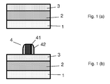
- a first preferred embodiment of the present disclosure is illustrated by means of figures 1 (a) to 1 (g) .
- a strained buffer layer 2 is epitaxially grown on a silicon substrate 1, a strained buffer layer 2 is epitaxially grown.
- the strained buffer layer 2 can comprise or consist for instance of SiGe or Si:C.
- a channel layer 3 is epitaxially grown on top of the strained buffer layer 2 ( Fig. 1(a) ).
- the channel layer 3 can for instance comprise or consist of Si or SiGe.
- a dummy gate structure 4 is provided on top of the channel layer 3 ( Fig. 1(b) ).
- the dummy gate structure can comprise for instance a silicon dummy gate 41 and a set of spacers 42. Dummy gate structures, their materials and methods to form them are known in the art.
- the dummy gate structure 4 is then used as an etching mask, for a selective etching process, as illustrated in Fig. 1(c) .
- a selective etching process is performed etching the channel layer 3 and at least part of the strained buffer layer 2.
- the etching process should hereby not or only to a very limited extend affect the dummy gate structure.
- spaces 50 are created above an exposed upper surface of the strained layer, abutting the sidewalls of a protrusion 6 formed by the etching process, which extends from the substrate 1.
- This protrusion thus comprises a portion of the channel layer 3 and at least an upper portion of the epitaxially grown strained layer 2.
- the sidewalls of the protrusion 6 can be straight, i.e.
- the profile of the sidewalls can have a curvature c for example can be inwardly curved, or can be outwardly curved. This nature of this curvature c can be predetermined by selecting appropriate etching chemistries and materials for the layer stack. The skilled person is aware of options for these etching chemistries and processes.
- source and drain structures 5 are grown epitaxially directly adjacent to the protrusion 6, at opposite sides thereof, on the sidewalls of the protrusion 6 as well as on the exposed upper surface of the strained layer 2, as illustrated in Fig.1(f) for instance.
- These structures can for instance comprise SiGe or Si:C.
- a physical interface between the source and drain regions and the protrusion's sidewalls is hereby created.
- the source and drain structures may further introduce stress in the channel layer 3.
- the overall introduced stress in the channel layer 3 can be controlled, and may be predetermined by an appropriate selection of materials and process conditions.
- the dummy gate structure 4 can now be replaced by a final gate structure 7.
- the dummy gate 41 is selectively removed and replaced by a final gate stack comprising at least a dielectric layer 73 and a metal layer or layer stack 74 ( Fig. 1(g) ).
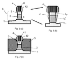
- a similar method is performed, with the difference that the selective etching step, which may comprise a sequence of different etching processes, is performed completely through the strained layer 2 ( Fig 2(a) ) and partially into the underlying substrate 1, creating spaces above an exposed upper surface of the the substrate, abutting the sidewalls of a protrusion 6 formed by the etching process.
- the protrusion 6 then also comprises an upper portion of the underlying substrate 1.
- the upper portion of the substrate is now also able to contribute in the stress redistribution.
- curvature c* (curvature c1* for portion of substrate 1, curvature c2* for portion of layer 2 and c 3 * for portion of layer 3) after elastic relaxation of the layers.
- source and drain structures 5 are grown epitaxially directly adjacent to the protrusion 6 , at opposite sides thereof, on the sidewalls of the protrusion as well as on the exposed upper surface of the substrate, as illustrated in Fig.2(c) , similar as in the first embodiment.
- a physical interface between the source and drain regions and the protrusion's sidewalls is hereby created.
- the dummy gate structure 4 is then replaced by a final gate structure 7.
- the dummy gate 41 is selectively removed and replaced by a final gate stack comprising at least a dielectric layer 73 and a metal layer or layer stack 74 ( Fig. 2(d) and (e) ).
- a third embodiment of the present disclosure is disclosed in Fig. 3(a) to (c) , which is similar to the first embodiment, but instead of providing a dummy gate structure 4 and replacing it with a final gate structure later on in the process flow, a final gate structure 7 is provided directly.
- An etching step is performed etching selectively into the channel layer and partially in the epitaxially grown strained layer, thereby using the final gate structure 7 as a mask ( Fig. 3 (a) and (b) ), and thereby creating a protrusion 6 extending from the substrate 1, the protrusion 6 comprising a portion of the channel layer 3 and at least an upper portion of the epitaxially grown strained layer 2, allowing elastic relaxation in these portions.
- the selective etching step which may comprise a sequence of different etching processes, is performed completely through the strained layer 2 and partially into the underlying substrate 1, similar as to what is described for the second embodiment of the present disclosure.
- source and drain structures 5 are grown epitaxially directly adjacent to the protrusion 6, at opposite sides thereof, on the sidewalls of the protrusion as well as on the exposed upper surface of the underlying layer, for instance the strained layer or substrate, as illustrated in Fig.3(c) , similar as in the first and second embodiments.
- a physical interface between the source and drain regions and the protrusion's sidewalls is hereby created.
- the transistor device is of the nFET type, wherein the epitaxially grown strained layer comprises SiGe with a germanium concentration in between 20 and 60%, wherein the channel layer comprises Silicon, and wherein the source and drain structures comprise Si:C, with a concentration of C being in between 0 and 5%.
- the transistor device is of the pFET type, wherein the epitaxially grown strained layer comprises Si:C, with a concentration of C being in between 0 and 5%, wherein the channel layer comprises Silicon, and where the source and drain structures comprise SiGe with a germanium concentration in between 20 and 60%.
- the transistor device is of the pFET type, wherein the epitaxially grown strained layer comprises SiGe with a Germanium concentration of about 25%, wherein the channel layer comprises SiGe with a Germanium concentration higher than 30 % (e.g. about 50%), and where the source and drain structures comprise SiGe with a germanium concentration in between 20 and 60%.
- the transistor device is of the nFET type, wherein the epitaxially grown strained layer comprises InAs, wherein the channel layer comprises InGaAs, comprising about 53% In, and about 47% Ga, and wherein the source and drain structures comprise InGaAs, comprising about 30% In, and about 70% Ga.
- the transistor device is of the nFET type, wherein the epitaxially grown strained layer comprises In y Ga 1-y As, wherein the channel layer comprises In x Ga 1-x As, with y>x, and wherein the source and drain structures comprise In z Ga 1-z As, with z ⁇ y, and x,y and z being values in the range of [0,1].
- the transistor device is of the nFET type, wherein the epitaxially grown strained layer comprises InGaAs, comprising about 70% In, and about 30% Ga, wherein the channel layer comprises InGaAs, comprising about 53% In, and about 47% Ga, and wherein the source and drain structures comprise InGaAs, comprising about 30% In, and about 70% Ga.
Landscapes
- Insulated Gate Type Field-Effect Transistor (AREA)
- Physics & Mathematics (AREA)
- Engineering & Computer Science (AREA)
- Plasma & Fusion (AREA)
- Chemical & Material Sciences (AREA)
- Crystallography & Structural Chemistry (AREA)
- Junction Field-Effect Transistors (AREA)
- Semiconductor Memories (AREA)
Priority Applications (1)
| Application Number | Priority Date | Filing Date | Title |
|---|---|---|---|
| EP15159942.0A EP2930752A3 (de) | 2014-04-08 | 2015-03-19 | Verfahren zur herstellung einer transistorvorrichtung. |
Applications Claiming Priority (2)
| Application Number | Priority Date | Filing Date | Title |
|---|---|---|---|
| EP14163805 | 2014-04-08 | ||
| EP15159942.0A EP2930752A3 (de) | 2014-04-08 | 2015-03-19 | Verfahren zur herstellung einer transistorvorrichtung. |
Publications (2)
| Publication Number | Publication Date |
|---|---|
| EP2930752A2 true EP2930752A2 (de) | 2015-10-14 |
| EP2930752A3 EP2930752A3 (de) | 2016-01-20 |
Family
ID=50439278
Family Applications (1)
| Application Number | Title | Priority Date | Filing Date |
|---|---|---|---|
| EP15159942.0A Withdrawn EP2930752A3 (de) | 2014-04-08 | 2015-03-19 | Verfahren zur herstellung einer transistorvorrichtung. |
Country Status (3)
| Country | Link |
|---|---|
| US (1) | US9406777B2 (de) |
| EP (1) | EP2930752A3 (de) |
| KR (1) | KR102284651B1 (de) |
Cited By (1)
| Publication number | Priority date | Publication date | Assignee | Title |
|---|---|---|---|---|
| CN107230701A (zh) * | 2016-03-25 | 2017-10-03 | 台湾积体电路制造股份有限公司 | 半导体器件及其制造方法 |
Families Citing this family (8)
| Publication number | Priority date | Publication date | Assignee | Title |
|---|---|---|---|---|
| US9972711B2 (en) * | 2015-06-03 | 2018-05-15 | International Business Machines Corporation | Reduced resistance short-channel InGaAs planar MOSFET |
| EP3437137A4 (de) * | 2016-04-01 | 2019-11-27 | INTEL Corporation | Indiumhaltige flosse eines transistors mit einem indiumreichen kern |
| CN107403835B (zh) * | 2016-05-19 | 2021-12-14 | 联芯集成电路制造(厦门)有限公司 | 半导体装置及其制作工艺 |
| US10134902B2 (en) * | 2016-12-15 | 2018-11-20 | Taiwan Semiconductor Manufacturing Company, Ltd. | PMOS FinFET |
| US10020398B1 (en) * | 2017-01-11 | 2018-07-10 | International Business Machines Corporation | Stress induction in 3D device channel using elastic relaxation of high stress material |
| KR102391512B1 (ko) | 2017-08-17 | 2022-04-27 | 삼성전자주식회사 | 반도체 소자 |
| KR102501097B1 (ko) * | 2018-06-21 | 2023-02-16 | 삼성전자주식회사 | 반도체 장치 및 반도체 장치의 제조 방법 |
| CN116646401B (zh) * | 2023-07-19 | 2024-01-23 | 成都蓉矽半导体有限公司 | 一种碳化硅异质结的共源共栅mosfet器件 |
Family Cites Families (14)
| Publication number | Priority date | Publication date | Assignee | Title |
|---|---|---|---|---|
| JPH07226501A (ja) | 1993-11-22 | 1995-08-22 | Lg Semicon Co Ltd | Mosトランジスタの製造方法 |
| US6963078B2 (en) | 2003-03-15 | 2005-11-08 | International Business Machines Corporation | Dual strain-state SiGe layers for microelectronics |
| US7019326B2 (en) * | 2003-11-14 | 2006-03-28 | Intel Corporation | Transistor with strain-inducing structure in channel |
| EP1638149B1 (de) * | 2004-09-15 | 2011-11-23 | STMicroelectronics (Crolles 2) SAS | Verfahren zur Herstellung eines Feldefekttransistors mit isoliertem Gatter und Heterostruktur-Kanal |
| US20060151787A1 (en) | 2005-01-12 | 2006-07-13 | International Business Machines Corporation | LOW CONCENTRATION SiGe BUFFER DURING STRAINED Si GROWTH OF SSGOI MATERIAL FOR DOPANT DIFFUSION CONTROL AND DEFECT REDUCTION |
| JP2007288165A (ja) | 2006-03-20 | 2007-11-01 | Goto Ikueikai | 歪み緩和バッファー層の製造方法及び歪み緩和バッファー層を備えた積層体 |
| US7608489B2 (en) * | 2006-04-28 | 2009-10-27 | International Business Machines Corporation | High performance stress-enhance MOSFET and method of manufacture |
| US7560326B2 (en) * | 2006-05-05 | 2009-07-14 | International Business Machines Corporation | Silicon/silcion germaninum/silicon body device with embedded carbon dopant |
| US7648853B2 (en) | 2006-07-11 | 2010-01-19 | Asm America, Inc. | Dual channel heterostructure |
| JP2010171337A (ja) * | 2009-01-26 | 2010-08-05 | Toshiba Corp | 電界効果トランジスタ |
| US8962400B2 (en) * | 2011-07-07 | 2015-02-24 | Taiwan Semiconductor Manufacturing Company, Ltd. | In-situ doping of arsenic for source and drain epitaxy |
| WO2013154574A1 (en) | 2012-04-13 | 2013-10-17 | Intel Corporation | Conversion of strain-inducing buffer to electrical insulator |
| CN104517847B (zh) * | 2013-09-29 | 2017-07-14 | 中芯国际集成电路制造(上海)有限公司 | 无结晶体管及其形成方法 |
| US9184290B2 (en) * | 2014-04-02 | 2015-11-10 | International Business Machines Corporation | Method of forming well-controlled extension profile in MOSFET by silicon germanium based sacrificial layer |
-
2015
- 2015-03-19 EP EP15159942.0A patent/EP2930752A3/de not_active Withdrawn
- 2015-03-23 KR KR1020150040204A patent/KR102284651B1/ko active Active
- 2015-03-24 US US14/667,376 patent/US9406777B2/en active Active
Non-Patent Citations (1)
| Title |
|---|
| None |
Cited By (2)
| Publication number | Priority date | Publication date | Assignee | Title |
|---|---|---|---|---|
| CN107230701A (zh) * | 2016-03-25 | 2017-10-03 | 台湾积体电路制造股份有限公司 | 半导体器件及其制造方法 |
| CN107230701B (zh) * | 2016-03-25 | 2021-10-15 | 台湾积体电路制造股份有限公司 | 半导体器件及其制造方法 |
Also Published As
| Publication number | Publication date |
|---|---|
| KR20150116771A (ko) | 2015-10-16 |
| US9406777B2 (en) | 2016-08-02 |
| EP2930752A3 (de) | 2016-01-20 |
| US20150287807A1 (en) | 2015-10-08 |
| KR102284651B1 (ko) | 2021-08-03 |
Similar Documents
| Publication | Publication Date | Title |
|---|---|---|
| US9406777B2 (en) | Method for manufacturing a transistor device | |
| KR101115091B1 (ko) | 상이한 격자 상수를 갖는 재료들을 구비한 반도체 구조체및 그 형성 방법 | |
| US20160190304A1 (en) | Defect-free strain relaxed buffer layer | |
| KR101865754B1 (ko) | 반도체 장치 및 그 제조 방법 | |
| US20160005657A1 (en) | Semiconductor structure with increased space and volume between shaped epitaxial structures | |
| KR20150059633A (ko) | 누설이 감소된 cmos 디바이스 및 그 형성 방법 | |
| US8552503B2 (en) | Strained silicon structure | |
| US9633891B2 (en) | Method for forming a transistor structure comprising a fin-shaped channel structure | |
| US9117777B2 (en) | Methods for manufacturing semiconductor devices | |
| US20170062215A1 (en) | Contact structure and extension formation for iii-v nfet | |
| US9349594B1 (en) | Non-planar semiconductor device with aspect ratio trapping | |
| KR102142587B1 (ko) | 응력 변형된 반도체 구조물 형성 방법 | |
| US20210013112A1 (en) | Vertical field-effect transistor (vfet) devices and methods of forming the same | |
| US20150162435A1 (en) | Asymmetric channel growth of a cladding layer over fins of a field effect transistor (finfet) device | |
| US20150311120A1 (en) | Fabricating field effect transistor(s) with stressed channel region(s) and low-resistance source/drain regions | |
| US20060081876A1 (en) | Process for fabricating a heterostructure-channel insulated-gate field-effect transistor, and the corresponding transistor | |
| US20170263495A1 (en) | Co-manufacturing method of zones with different uniaxial stresses | |
| US10615178B2 (en) | Dual-material mandrel for epitaxial crystal growth on silicon | |
| KR101587430B1 (ko) | 실리콘(001) 기판 상에 반도체 에피층 성장방법 | |
| KR101556090B1 (ko) | 실리콘(001) 기판 상에 다종의 반도체 에피층 성장방법 | |
| US8329551B2 (en) | Semiconductor device substrate with embedded stress region, and related fabrication methods | |
| KR20150059351A (ko) | Ge 및/또는 III-V족 화합물 반도체를 이용한 반도체 소자 및 그 제조방법 | |
| Wang et al. | Integration of Selective Epitaxial Growth of SiGe/Ge Layers in 14nm Node FinFETs | |
| EP2693462B1 (de) | Herstellungsverfahren für Halbleitervorrichtungen | |
| JP5711805B1 (ja) | 半導体デバイスの製造方法 |
Legal Events
| Date | Code | Title | Description |
|---|---|---|---|
| PUAI | Public reference made under article 153(3) epc to a published international application that has entered the european phase |
Free format text: ORIGINAL CODE: 0009012 |
|
| AK | Designated contracting states |
Kind code of ref document: A2 Designated state(s): AL AT BE BG CH CY CZ DE DK EE ES FI FR GB GR HR HU IE IS IT LI LT LU LV MC MK MT NL NO PL PT RO RS SE SI SK SM TR |
|
| AX | Request for extension of the european patent |
Extension state: BA ME |
|
| PUAL | Search report despatched |
Free format text: ORIGINAL CODE: 0009013 |
|
| AK | Designated contracting states |
Kind code of ref document: A3 Designated state(s): AL AT BE BG CH CY CZ DE DK EE ES FI FR GB GR HR HU IE IS IT LI LT LU LV MC MK MT NL NO PL PT RO RS SE SI SK SM TR |
|
| AX | Request for extension of the european patent |
Extension state: BA ME |
|
| RIC1 | Information provided on ipc code assigned before grant |
Ipc: H01L 29/10 20060101AFI20151215BHEP Ipc: H01L 29/66 20060101ALI20151215BHEP Ipc: H01L 29/78 20060101ALI20151215BHEP |
|
| STAA | Information on the status of an ep patent application or granted ep patent |
Free format text: STATUS: THE APPLICATION IS DEEMED TO BE WITHDRAWN |
|
| 18D | Application deemed to be withdrawn |
Effective date: 20160721 |