EP2922192A1 - Power converter, power generating system, apparatus for controlling power converter, and method for controlling power converter - Google Patents
Power converter, power generating system, apparatus for controlling power converter, and method for controlling power converter Download PDFInfo
- Publication number
- EP2922192A1 EP2922192A1 EP15152604.3A EP15152604A EP2922192A1 EP 2922192 A1 EP2922192 A1 EP 2922192A1 EP 15152604 A EP15152604 A EP 15152604A EP 2922192 A1 EP2922192 A1 EP 2922192A1
- Authority
- EP
- European Patent Office
- Prior art keywords
- voltage
- output
- boost circuit
- unit
- phase inverter
- Prior art date
- Legal status (The legal status is an assumption and is not a legal conclusion. Google has not performed a legal analysis and makes no representation as to the accuracy of the status listed.)
- Withdrawn
Links
Images


Classifications
-
- H—ELECTRICITY
- H02—GENERATION; CONVERSION OR DISTRIBUTION OF ELECTRIC POWER
- H02M—APPARATUS FOR CONVERSION BETWEEN AC AND AC, BETWEEN AC AND DC, OR BETWEEN DC AND DC, AND FOR USE WITH MAINS OR SIMILAR POWER SUPPLY SYSTEMS; CONVERSION OF DC OR AC INPUT POWER INTO SURGE OUTPUT POWER; CONTROL OR REGULATION THEREOF
- H02M7/00—Conversion of AC power input into DC power output; Conversion of DC power input into AC power output
- H02M7/42—Conversion of DC power input into AC power output without possibility of reversal
- H02M7/44—Conversion of DC power input into AC power output without possibility of reversal by static converters
- H02M7/48—Conversion of DC power input into AC power output without possibility of reversal by static converters using discharge tubes with control electrode or semiconductor devices with control electrode
- H02M7/53—Conversion of DC power input into AC power output without possibility of reversal by static converters using discharge tubes with control electrode or semiconductor devices with control electrode using devices of a triode or transistor type requiring continuous application of a control signal
- H02M7/537—Conversion of DC power input into AC power output without possibility of reversal by static converters using discharge tubes with control electrode or semiconductor devices with control electrode using devices of a triode or transistor type requiring continuous application of a control signal using semiconductor devices only, e.g. single switched pulse inverters
- H02M7/5387—Conversion of DC power input into AC power output without possibility of reversal by static converters using discharge tubes with control electrode or semiconductor devices with control electrode using devices of a triode or transistor type requiring continuous application of a control signal using semiconductor devices only, e.g. single switched pulse inverters in a bridge configuration
- H02M7/53871—Conversion of DC power input into AC power output without possibility of reversal by static converters using discharge tubes with control electrode or semiconductor devices with control electrode using devices of a triode or transistor type requiring continuous application of a control signal using semiconductor devices only, e.g. single switched pulse inverters in a bridge configuration with automatic control of output voltage or current
-
- H—ELECTRICITY
- H02—GENERATION; CONVERSION OR DISTRIBUTION OF ELECTRIC POWER
- H02M—APPARATUS FOR CONVERSION BETWEEN AC AND AC, BETWEEN AC AND DC, OR BETWEEN DC AND DC, AND FOR USE WITH MAINS OR SIMILAR POWER SUPPLY SYSTEMS; CONVERSION OF DC OR AC INPUT POWER INTO SURGE OUTPUT POWER; CONTROL OR REGULATION THEREOF
- H02M7/00—Conversion of AC power input into DC power output; Conversion of DC power input into AC power output
- H02M7/42—Conversion of DC power input into AC power output without possibility of reversal
- H02M7/44—Conversion of DC power input into AC power output without possibility of reversal by static converters
- H02M7/48—Conversion of DC power input into AC power output without possibility of reversal by static converters using discharge tubes with control electrode or semiconductor devices with control electrode
- H02M7/53—Conversion of DC power input into AC power output without possibility of reversal by static converters using discharge tubes with control electrode or semiconductor devices with control electrode using devices of a triode or transistor type requiring continuous application of a control signal
- H02M7/537—Conversion of DC power input into AC power output without possibility of reversal by static converters using discharge tubes with control electrode or semiconductor devices with control electrode using devices of a triode or transistor type requiring continuous application of a control signal using semiconductor devices only, e.g. single switched pulse inverters
- H02M7/5387—Conversion of DC power input into AC power output without possibility of reversal by static converters using discharge tubes with control electrode or semiconductor devices with control electrode using devices of a triode or transistor type requiring continuous application of a control signal using semiconductor devices only, e.g. single switched pulse inverters in a bridge configuration
-
- G—PHYSICS
- G05—CONTROLLING; REGULATING
- G05F—SYSTEMS FOR REGULATING ELECTRIC OR MAGNETIC VARIABLES
- G05F1/00—Automatic systems in which deviations of an electric quantity from one or more predetermined values are detected at the output of the system and fed back to a device within the system to restore the detected quantity to its predetermined value or values, i.e. retroactive systems
- G05F1/10—Regulating voltage or current
- G05F1/46—Regulating voltage or current wherein the variable actually regulated by the final control device is DC
- G05F1/56—Regulating voltage or current wherein the variable actually regulated by the final control device is DC using semiconductor devices in series with the load as final control devices
- G05F1/563—Regulating voltage or current wherein the variable actually regulated by the final control device is DC using semiconductor devices in series with the load as final control devices including two stages of regulation at least one of which is output level responsive, e.g. coarse and fine regulation
-
- G—PHYSICS
- G05—CONTROLLING; REGULATING
- G05F—SYSTEMS FOR REGULATING ELECTRIC OR MAGNETIC VARIABLES
- G05F1/00—Automatic systems in which deviations of an electric quantity from one or more predetermined values are detected at the output of the system and fed back to a device within the system to restore the detected quantity to its predetermined value or values, i.e. retroactive systems
- G05F1/10—Regulating voltage or current
- G05F1/46—Regulating voltage or current wherein the variable actually regulated by the final control device is DC
- G05F1/607—Regulating voltage or current wherein the variable actually regulated by the final control device is DC using discharge tubes in parallel with the load as final control devices
- G05F1/61—Regulating voltage or current wherein the variable actually regulated by the final control device is DC using discharge tubes in parallel with the load as final control devices including two stages of regulation, at least one of which is output level responsive
-
- H—ELECTRICITY
- H02—GENERATION; CONVERSION OR DISTRIBUTION OF ELECTRIC POWER
- H02M—APPARATUS FOR CONVERSION BETWEEN AC AND AC, BETWEEN AC AND DC, OR BETWEEN DC AND DC, AND FOR USE WITH MAINS OR SIMILAR POWER SUPPLY SYSTEMS; CONVERSION OF DC OR AC INPUT POWER INTO SURGE OUTPUT POWER; CONTROL OR REGULATION THEREOF
- H02M1/00—Details of apparatus for conversion
- H02M1/08—Circuits specially adapted for the generation of control voltages for semiconductor devices incorporated in static converters
-
- H—ELECTRICITY
- H02—GENERATION; CONVERSION OR DISTRIBUTION OF ELECTRIC POWER
- H02M—APPARATUS FOR CONVERSION BETWEEN AC AND AC, BETWEEN AC AND DC, OR BETWEEN DC AND DC, AND FOR USE WITH MAINS OR SIMILAR POWER SUPPLY SYSTEMS; CONVERSION OF DC OR AC INPUT POWER INTO SURGE OUTPUT POWER; CONTROL OR REGULATION THEREOF
- H02M1/00—Details of apparatus for conversion
- H02M1/12—Arrangements for reducing harmonics from AC input or output
- H02M1/126—Arrangements for reducing harmonics from AC input or output using passive filters
-
- H—ELECTRICITY
- H02—GENERATION; CONVERSION OR DISTRIBUTION OF ELECTRIC POWER
- H02M—APPARATUS FOR CONVERSION BETWEEN AC AND AC, BETWEEN AC AND DC, OR BETWEEN DC AND DC, AND FOR USE WITH MAINS OR SIMILAR POWER SUPPLY SYSTEMS; CONVERSION OF DC OR AC INPUT POWER INTO SURGE OUTPUT POWER; CONTROL OR REGULATION THEREOF
- H02M3/00—Conversion of DC power input into DC power output
- H02M3/02—Conversion of DC power input into DC power output without intermediate conversion into AC
- H02M3/04—Conversion of DC power input into DC power output without intermediate conversion into AC by static converters
- H02M3/10—Conversion of DC power input into DC power output without intermediate conversion into AC by static converters using discharge tubes with control electrode or semiconductor devices with control electrode
- H02M3/145—Conversion of DC power input into DC power output without intermediate conversion into AC by static converters using discharge tubes with control electrode or semiconductor devices with control electrode using devices of a triode or transistor type requiring continuous application of a control signal
- H02M3/155—Conversion of DC power input into DC power output without intermediate conversion into AC by static converters using discharge tubes with control electrode or semiconductor devices with control electrode using devices of a triode or transistor type requiring continuous application of a control signal using semiconductor devices only
- H02M3/156—Conversion of DC power input into DC power output without intermediate conversion into AC by static converters using discharge tubes with control electrode or semiconductor devices with control electrode using devices of a triode or transistor type requiring continuous application of a control signal using semiconductor devices only with automatic control of output voltage or current, e.g. switching regulators
- H02M3/158—Conversion of DC power input into DC power output without intermediate conversion into AC by static converters using discharge tubes with control electrode or semiconductor devices with control electrode using devices of a triode or transistor type requiring continuous application of a control signal using semiconductor devices only with automatic control of output voltage or current, e.g. switching regulators including plural semiconductor devices as final control devices for a single load
-
- H—ELECTRICITY
- H02—GENERATION; CONVERSION OR DISTRIBUTION OF ELECTRIC POWER
- H02M—APPARATUS FOR CONVERSION BETWEEN AC AND AC, BETWEEN AC AND DC, OR BETWEEN DC AND DC, AND FOR USE WITH MAINS OR SIMILAR POWER SUPPLY SYSTEMS; CONVERSION OF DC OR AC INPUT POWER INTO SURGE OUTPUT POWER; CONTROL OR REGULATION THEREOF
- H02M1/00—Details of apparatus for conversion
- H02M1/0048—Circuits or arrangements for reducing losses
- H02M1/0054—Transistor switching losses
-
- H—ELECTRICITY
- H02—GENERATION; CONVERSION OR DISTRIBUTION OF ELECTRIC POWER
- H02M—APPARATUS FOR CONVERSION BETWEEN AC AND AC, BETWEEN AC AND DC, OR BETWEEN DC AND DC, AND FOR USE WITH MAINS OR SIMILAR POWER SUPPLY SYSTEMS; CONVERSION OF DC OR AC INPUT POWER INTO SURGE OUTPUT POWER; CONTROL OR REGULATION THEREOF
- H02M1/00—Details of apparatus for conversion
- H02M1/0067—Converter structures employing plural converter units, other than for parallel operation of the units on a single load
- H02M1/007—Plural converter units in cascade
-
- Y—GENERAL TAGGING OF NEW TECHNOLOGICAL DEVELOPMENTS; GENERAL TAGGING OF CROSS-SECTIONAL TECHNOLOGIES SPANNING OVER SEVERAL SECTIONS OF THE IPC; TECHNICAL SUBJECTS COVERED BY FORMER USPC CROSS-REFERENCE ART COLLECTIONS [XRACs] AND DIGESTS
- Y02—TECHNOLOGIES OR APPLICATIONS FOR MITIGATION OR ADAPTATION AGAINST CLIMATE CHANGE
- Y02B—CLIMATE CHANGE MITIGATION TECHNOLOGIES RELATED TO BUILDINGS, e.g. HOUSING, HOUSE APPLIANCES OR RELATED END-USER APPLICATIONS
- Y02B70/00—Technologies for an efficient end-user side electric power management and consumption
- Y02B70/10—Technologies improving the efficiency by using switched-mode power supplies [SMPS], i.e. efficient power electronics conversion e.g. power factor correction or reduction of losses in power supplies or efficient standby modes
Definitions
- the embodiments discussed herein are directed to a power converter, a power generating system, an apparatus for controlling a power converter, and a method for controlling a power converter.
- power converters that include a boost circuit and a single-phase inverter, and in which the single-phase inverter outputs an alternating-current (AC) voltage with a higher amplitude than that of a direct-current (DC) power source, by causing the boost circuit to boost the voltage of the DC power source.
- AC alternating-current
- DC direct-current
- Such a power converter causes the single-phase inverter to generate a part of the AC voltage waveform in which the absolute value of the voltage is lower than the DC power source voltage, and causes the boost circuit to generate a part of the AC voltage waveform in which the absolute value of the voltage is higher than the DC power source voltage (see International Publication WO 2013/069326 , for example).
- One aspect of embodiments is made in consideration of the above, and an object of the embodiment is to provide a power converter, a power generating system, an apparatus for controlling a power converter, and a method for controlling a power converter capable of suppressing the distortion in the AC voltage output from the single-phase inverter when switching is performed from the boosting operation in the boost circuit to the PWM operation in the single-phase inverter.
- a power converter includes a boost circuit, a single-phase inverter, and a controller.
- the boost circuit boosts a voltage of a direct-current (DC) power source.
- the single-phase inverter converts a voltage output from the boost circuit into an alternating-current (AC) voltage, and outputs the AC voltage.
- the controller includes a voltage detection filter and a detected voltage modifying unit. The voltage detection filter removes a noise component from a detection result of a voltage detector which detects the output voltage of the boost circuit.
- the detected voltage modifying unit modifies an output from the voltage detection filter based on a delay compensating value for compensating a detection delay introduced by the voltage detection filter, when switching is performed from the boosting operation in the boost circuit to the PWM operation in the single-phase inverter.
- An object of an aspect of embodiments is to provide a power converter, a power generating system, an apparatus for controlling a power converter, and a method for controlling a power converter capable of suppressing the distortion in the AC voltage output from the single-phase inverter when switching is performed from the boosting operation in the boost circuit to the PWM operation in the single-phase inverter.
- a solar cell is used as an example of a direct-current (DC) power source and a power generator, but the DC power source and the power generator may be a DC power generator or a fuel cell, without limitation to a solar cell.
- the DC power source may be, for example, an alternating-current (AC) power source (including an AC power generator) provided with a converter, and in which the converter converts the AC power from the AC power source into a DC power and outputs the DC power.
- AC alternating-current
- FIG. 1 is a schematic illustrating an example of a configuration of a power generating system according to a first embodiment.
- the power generating system 1 according to the first embodiment includes a power converter 2 and a solar cell 3.
- the power converter 2 converts the DC power generated by the solar cell 3 into AC power, and outputs the AC power to an electrical grid 4.
- the power converter 2 is connected to the electrical grid 4, but the power converter 2 may be connected to any load, without limitation to the electrical grid 4, e.g., a device operating with the AC power.
- the power converter 2 includes input terminals Tp and Tn, output terminals T1 and T2, a boost circuit 10, a single-phase inverter 11, an output filter 12, a power source current detector 13, a power source voltage detector 14, an output current detector 15, an output voltage detector 16, a bus voltage detector 17, and a controller 20 (an example of a controller and an apparatus for controlling a power converter).
- the input terminal Tp is connected to the cathode of the solar cell 3, and the input terminal Tn is connected to the anode of the solar cell 3.
- the output terminals T1 and T2 are connected to the electrical grid 4.
- the boost circuit 10 and the single-phase inverter 11 convert the DC voltage input from the solar cell 3, being input via the input terminals Tp and Tn, into an AC voltage, and the AC voltage after the conversion is output from the output terminals T1, T2 to the electrical grid 4.
- the boost circuit 10 includes switching elements Q5 and Q6, diodes D5 and D6, a reactor L1, and capacitors C1 and C2. One end of the reactor L1 is connected to the solar cell 3.
- the switching element Q5 is connected in parallel between the cathode and the anode of the solar cell 3, via the reactor L1.
- the diode D5 is connected in anti-parallel with the switching element Q5.
- One end of the switching element Q6 is connected to the connection point between the reactor L1 and the switching element Q5, and the other end is connected to the single-phase inverter 11.
- the diode D6 is connected in anti-parallel with the switching element Q6.
- the capacitor C1 is connected between the cathode and the anode of the solar cell 3, and controls the voltage fluctuation between the input terminals Tp and Tn.
- a capacitor C2 is connected to the output end of the boost circuit 10, and smoothes out the voltage boosted by the reactor L1 and the switching element Q5.
- the boost circuit 10 outputs a boosted voltage from the switching element Q6 by controlling to switch ON and OFF the switching elements Q5 and Q6 alternatingly, boosting the DC voltage input from the solar cell 3 via the input terminals Tp and Tn thereby.
- the boost circuit 10 outputs the DC voltage input from the solar cell 3 via the input terminals Tp and Tn from the switching element Q6, by controlling to switch OFF the switching element Q5 and to switch ON the switching element Q6.
- the boost circuit 10 is capable of boosting the DC voltage output from the solar cell 3, and of outputting the DC voltage output from the solar cell 3 without boosting.
- the voltage at the connection point between the boost circuit 10 and the single-phase inverter 11, that is, the voltage output from the boost circuit 10 and input to the single-phase inverter 11 is referred to as a bus voltage Vpn.
- the single-phase inverter 11 includes switching elements Q1 to Q4 that are bridge-connected, and switching elements Q1 to Q4 connected in anti-parallel with the respective diodes D1 to D4.
- the single-phase inverter 11 converts the bus voltage Vpn to a positive AC voltage by controlling to switch ON and OFF the switching element Q1 and Q4, and converts the bus voltage Vpn to a negative AC voltage by controlling to switch ON and OFF the switching elements Q2 and Q3.
- the single-phase inverter 11 outputs the bus voltage Vpn as a positive voltage by controlling to switch ON the switching elements Q1 and Q4, and outputs the bus voltage Vpn as a negative voltage by controlling to switch ON the switching elements Q2 and Q3.
- the single-phase inverter 11 is capable of converting the bus voltage Vpn into an AC voltage, and of outputting the bus voltage Vpn without converting.
- the switching elements Q1 to Q6 are made of a wide-bandgap semiconductor containing gallium nitride (GaN) or silicon carbide (SiC), for example.
- the switching elements Q1 to Q6 may also be metal-oxide-semiconductor field-effect transistors (MOSFETs) or insulated gate bipolar transistors (IGBTs).
- MOSFETs metal-oxide-semiconductor field-effect transistors
- IGBTs insulated gate bipolar transistors
- the output filter 12 is a LC filter including a reactor L2 and capacitor C3, for example, and is provided between the single-phase inverter 11 and the electrical grid 4.
- the output filter 12 removes the switching noise introduced by the switching elements Q1 to Q4 in the single-phase inverter 11.
- the power source current detector 13 detects an instantaneous current Iin of the DC supplied from the solar cell 3 to the boost circuit 10 (hereinafter, sometimes referred to as a power source current Iin).
- the power source voltage detector 14 detects the instantaneous value Vin of the DC voltage supplied from the solar cell 3 (hereinafter, sometimes referred to as a power source voltage Vin).
- the power source current detector 13 uses a Hall element, for example, that is a magneto-electric transducer in detecting the current.
- the output current detector 15 detects an instantaneous value ig of the AC supplied from the power converter 2 to the electrical grid 4 (hereinafter, sometimes referred to as an output current ig).
- the output voltage detector 16 detects an instantaneous value ug of the AC voltage supplied from the power converter 2 to the electrical grid 4 (hereinafter, sometimes referred to as an output voltage ug).
- the output current detector 15 uses a Hall element, for example, that is a magneto-electric transducer in detecting the current.
- the bus voltage detector 17 detects an instantaneous value of the bus voltage Vpn (hereinafter, sometimes referred to as bus voltage Vpn1) output from the boost circuit 10 to the single-phase inverter 11.
- the controller 20 outputs gate signals S1 to S6 for controlling the boost circuit 10 and the single-phase inverter 11 based on the power source voltage Vin, the power source current Iin, the output current ig, the output voltage ug, and the bus voltage Vpn1.
- the gate signals S1 to S6 are input to the gates of the respective switching elements Q1 to Q6, to control the switching elements Q1 to Q6, respectively.
- the controller 20 includes a microcomputer and various circuits, including a central processing unit (CPU), a read-only memory (ROM), a random access memory (RAM), and an input/output port, for example.
- the CPU in the microcomputer included in the controller 20 implements the control to be described later by reading the computer program stored in the ROM and executing the computer program, for example.
- a specific example of a configuration of the controller 20 will now be explained with reference to some drawings.
- FIG. 2 is a schematic illustrating an example of a configuration of the controller 20.
- the controller 20 includes a reference generating unit 21, a voltage detection filter 22, an inverter controlling unit 23, a boosting controlling unit 24, and a detected voltage modifying unit 25.
- the functions of the reference generating unit 21, the voltage detection filter 22, the inverter controlling unit 23, the boosting controlling unit 24, and the detected voltage modifying unit 25 are implemented by causing the CPU to read and to execute a computer program, for example.
- At least some or all of the reference generating unit 21, the voltage detection filter 22, the inverter controlling unit 23, the boosting controlling unit 24, and the detected voltage modifying unit 25 may be implemented as an integrated circuit such as an application specific integrated circuit (ASIC) or a field programmable gate array (FPGA).
- ASIC application specific integrated circuit
- FPGA field programmable gate array
- the reference generating unit 21 generates an AC voltage reference Ug* for maximizing the power supplied from the solar cell 3 to the boost circuit 10, based on the power source current Iin received from the power source current detector 13 and the power source voltage Vin received from the power source voltage detector 14. To maximize the power, the reference generating unit 21 outputs the AC voltage reference Ug* to the inverter controlling unit 23 or to the boosting controlling unit 24 based on a relation between the AC voltage reference Ug* and the power source voltage Vin.
- the reference generating unit 21 When the absolute value of the AC voltage reference Ug* is equal to or lower than the power source voltage Vin, the reference generating unit 21 outputs the AC voltage reference Ug* to the inverter controlling unit 23. When the absolute value of the AC voltage reference Ug* is higher than the power source voltage Vin, the reference generating unit 21 outputs the AC voltage reference Ug* to the boosting controlling unit 24.
- the reference generating unit 21 includes a phase detector 30, a coordinate converter 31, a dq converter 32, a current reference generator 33, subtractors 34 and 35, a q-axis current controller 36, a d-axis current controller 37, an AC voltage reference generator 38, a switching determining unit 39, and a switching unit 40.
- the phase detector 30 detects a phase ⁇ of the output voltage ug to be supplied from the power converter 2 to the electrical grid 4 (hereinafter, referred to as an output voltage phase ⁇ ).
- the phase detector 30 is configured as a phase locked loop (PLL), for example.
- PLL phase locked loop
- the output voltage ug corresponds to the voltage of the electrical grid 4.
- the coordinate converter 31 converts the output current ig to be supplied from the single-phase inverter 11 to the electrical grid 4 into a pair of signals orthogonally intersecting with each other in an orthogonal coordinate system. For example, the coordinate converter 31 generates a first signal synchronized with the phase of the output current ig, and a second signal delayed by 90 degrees with respect to the phase of the output current ig, based on the output current ig.
- the dq converter 32 performs a coordinate conversion of the first and the second signals generated by the coordinate converter 31, into dq components in a dq coordinate system, based on the output voltage phase ⁇ . As a result of this process, the dq converter 32 obtains a current Id of the d-axis component (hereinafter, referred to as a d-axis current Id) and a current Iq of the q-axis component (hereinafter, referred to as a q-axis current Iq).
- the q-axis current Iq corresponds to an active component of the output current ig
- the d-axis current Id corresponds to a reactive component of the output current ig.
- the current reference generator 33 generates a current reference i* for maximizing the power supplied from the solar cell 3 to the boost circuit 10 based on the power source voltage Vin and the power source current Iin.
- the current reference i* has a q-axis current reference Iq* as a q-axis component, and has a d-axis current reference Id* as a d-axis component.
- the q-axis current reference Iq* is a reference corresponding to the active component of the output current ig
- the d-axis current reference Id* is a reference corresponding to the reactive component of the output current ig.
- the subtractor 34 subtracts the q-axis current Iq from the q-axis current reference Iq* to obtain a q-axis current deviation Iqdiff, and outputs the q-axis current deviation Iqdiff to the q-axis current controller 36.
- the q-axis current controller 36 adjusts a q-axis AC voltage reference Uq* in such a manner that the q-axis current deviation Iqdiff becomes zero, by performing proportional-integral (PI) control, for example, and outputs the q-axis AC voltage reference Uq* to the AC voltage reference generator 38.
- PI proportional-integral
- the subtractor 35 subtracts the d-axis current Id from the d-axis current reference Id* to obtain a d-axis current deviation Iddiff, and outputs the d-axis current deviation Iddiff to the d-axis current controller 37.
- the d-axis current controller 37 adjusts a d-axis AC voltage reference Ud* in such a manner that the d-axis current deviation Iddiff becomes zero, by performing PI control, for example, and outputs the d-axis AC voltage reference Ud to the AC voltage reference generator 38.
- the switching determining unit 39 determines if the absolute value of the AC voltage reference Ug* is equal to or lower than the power source voltage Vin. If the switching determining unit 39 determines that the absolute value of the AC voltage reference Ug* is equal to or lower than the power source voltage Vin, the switching determining unit 39 outputs a Low-level switching signal Sw. If the switching determining unit 39 determines that the absolute value of the AC voltage reference Ug* is higher than the power source voltage Vin, the switching determining unit 39 outputs a High-level switching signal Sw.
- the switching unit 40 outputs the AC voltage reference Ug* either to the inverter controlling unit 23 or to the boosting controlling unit 24 based on the switching signal Sw. If the switching signal Sw is set to the Low level, the switching unit 40 outputs the AC voltage reference Ug* to the inverter controlling unit 23. If the switching signal Sw is set to the High level, the switching unit 40 outputs the AC voltage reference Ug* to the boosting controlling unit 24.
- the switching determining unit 39 may have any other configuration without limitation to the configuration illustrated in FIG. 2 .
- the switching unit 40 may not be provided, and the AC voltage reference Ug* may be input to the inverter controlling unit 23 and to the boosting controlling unit 24.
- the switching determining unit 39 may then select which one of the inverter controlling unit 23 and the boosting controlling unit 24 to operate.
- the inverter controlling unit 23 performs the control for the PWM operation in the single-phase inverter 11 if the switching signal Sw is set to the Low level, and does not perform the control for the PWM operation in the single-phase inverter 11 if the switching signal Sw is set to the High level.
- the boosting controlling unit 24 does not perform the control for the boosting operation in the boost circuit 10 if the switching signal Sw is set to the Low level, and performs the controls for the boosting operation in the boost circuit 10 if the switching signal Sw is set to the High level.
- the reference generating unit 21 may also have any other configuration without limitation to the configuration illustrated in FIG. 2 .
- the reference generating unit 21 may be provided with a reference generating unit for generating the AC voltage reference Ug* for the inverter controlling unit 23, and another reference generating unit for generating the AC voltage reference Ug* for the boosting controlling unit 24, separately.
- the voltage detection filter 22 removes a noise component from the bus voltage Vpn1 that is the detection result from the bus voltage detector 17 (see FIG. 1 ).
- the voltage detection filter 22 is a low-pass filter, for example.
- the voltage detection filter 22 removes a noise component (e.g., the frequency component equal to or higher than 100 hertz) from the bus voltage Vpn1.
- the bus voltage Vpn1 having a noise removed by the voltage detection filter 22 is referred to as a bus voltage Vpn2.
- the inverter controlling unit 23 generates gate signals S1 to S4 based on the bus voltage Vpn2, the power source voltage Vin, and the AC voltage reference Ug*.
- the inverter controlling unit 23 includes a voltage correcting unit 51 and a carrier comparing unit 52, as illustrated in FIG. 2 .
- the voltage correcting unit 51 obtains a modulation factor ⁇ 1 by correcting the AC voltage reference Ug* based on a reference voltage Vref and the bus voltage Vpn2.
- the voltage correcting unit 51 obtains the modulation factor ⁇ 1 by, for example, performing the operation of following Equation (3).
- the reference voltage Vref is parameter set to the voltage correcting unit 51 in advance.
- ⁇ ⁇ 1 Ug * ⁇ Vref Vpn ⁇ 2
- the carrier comparing unit 52 If the absolute value of the AC voltage reference Ug* is equal to or lower than the power source voltage Vin, the carrier comparing unit 52 generates a PWM signal by comparing the modulation factor ⁇ 1 with a carrier signal. If the AC voltage reference Ug* has a positive polarity, the carrier comparing unit 52 outputs the generated PWM signal as gate signals S1 and S4. If the AC voltage reference Ug* has a negative polarity, the carrier comparing unit 52 outputs the generated PWM signal as gate signals S2 and S3.
- the carrier comparing unit 52 outputs the gate signals S1 to S4 based on the polarity of the AC voltage reference Ug*. For example, if the AC voltage reference Ug* has a positive polarity, the carrier comparing unit 52 sets the gate signals S1 and S4 to the High level, and sets the gate signals S2 and S3 to the Low level. As a result, the single-phase inverter 11 is caused to output a positive voltage. If the AC voltage reference Ug* has a negative polarity, the carrier comparing unit 52 sets the gate signals S2 and S3 to the High level, and sets the gate signals S1 and S4 to the Low level. As a result, the single-phase inverter 11 is caused to output a negative voltage.
- the boosting controlling unit 24 If the absolute value of the AC voltage reference Ug* is equal to or lower than the power source voltage Vin, the boosting controlling unit 24 outputs a Low-level gate signal S5 and a High-level gate signal S6.
- the gate signal S5 switches OFF the switching element Q5, and the gate signal S6 switches ON the switching element Q6.
- the power source voltage Vin is therefore output to the single-phase inverter 11 via the reactor L1 and the switching element Q6.
- the boosting controlling unit 24 controls the boost circuit 10 to switch ON the switching elements Q5 and Q6 alternatingly during a period in which generated is a portion (an example of a first portion) of the output voltage ug of which the absolute value is higher than the power source voltage Vin. In this manner, even if the load on the power converter 2 becomes low or absent during the period in which generated is a portion of the output voltage ug of which the absolute value is higher than the power source voltage Vin, the charge at the capacitor C1 bringing up the bus voltage Vpn unnecessarily high can be released to the side of the solar cell 3 via the switching element Q6 and the reactor L1.
- FIG. 3 is a schematic illustrating an example of a relation between the gate signals S1 to S6 output from the inverter controlling unit 23 and the boosting controlling unit 24, the output voltage ug, and the bus voltage Vpn.
- the power converter 2 if the absolute value of the AC voltage reference Ug* is equal to or lower than the power source voltage Vin, the power converter 2 outputs a voltage based on the AC voltage reference Ug*, by not causing the boost circuit 10 to perform the boosting operation, but by causing the single-phase inverter 11 to perform the PWM operation.
- the inverter controlling unit 23 causes the single-phase inverter 11 to output a positive voltage by switching ON one of the switching elements Q1 and Q4, and switching ON and OFF the other.
- the inverter controlling unit 23 causes the single-phase inverter 11 to output a negative voltage by switching ON one of the switching elements Q2 and Q3, and switching ON and OFF the other. In this manner, the portion (an example of a second portion) of the output voltage ug of which the absolute value is lower than the power source voltage Vin is generated.
- the power converter 2 causes the boost circuit 10 to perform the boosting operation, and does not cause the single-phase inverter 11 to perform the PWM operation.
- This boosting operation allows the power converter 2 to output a bus voltage Vpn based on the AC voltage reference Ug* to the electrical grid 4 via the single-phase inverter 11. In this manner, the portion of the output voltage ug of which the absolute value of the AC voltage reference Ug* is higher than the power source voltage Vin is generated.
- the detected voltage modifying unit 25 modifies the output from the voltage detection filter 22 based on a delay compensating value Vcmp for compensating a detection delay in the voltage detection filter 22. In this manner, a distortion in the output voltage ug to be output from the single-phase inverter 11 can be suppressed, the distortion being a result of switching the control from the boosting operation to the inverter operation.
- FIG. 4 is a schematic illustrating a detection delay in the voltage detection filter 22.
- FIG. 5 is a schematic illustrating a distortion in the output voltage resulting from the detection delay.
- the boost circuit 10 is used to generate a part of the AC output voltage ug in which the absolute value of the AC voltage reference Ug* is higher than the power source voltage Vin.
- the voltage detection filter 22 has some detection delay. Therefore, if there is a change in the bus voltage Vpn during the period of the boosting control, a change in the bus voltage Vpn2 is delayed as well, as illustrated in FIG. 4 . As a result, when the control is switched from the boosting operation in the boost circuit 10 to the PWM operation in the single-phase inverter 11, the bus voltage Vpn2 output from the voltage detection filter 22 includes some error ⁇ Vpn.
- the inverter controlling unit 23 performs the PWM control based on the bus voltage Vpn2
- the output voltage ug changes abruptly due to the error ⁇ Vpn, as illustrated in FIG. 5
- the output voltage ug becomes distorted.
- the bus voltage Vpn2 would still have the error ⁇ Vpn.
- the resultant output voltage ug therefore becomes distorted as well, in the same manner as when the filtering function of the voltage detection filter 22 is always kept ON.
- the detected voltage modifying unit 25 modifies the output from the voltage detection filter 22 based on the delay compensating value Vcmp for compensating the detection delay in the voltage detection filter 22, when the control is switched from the boosting operation in the boost circuit 10 to the PWM operation in the single-phase inverter 11.
- the detected voltage modifying unit 25 calculates an estimated bus voltage Vpn ⁇ by estimating a voltage drop ⁇ V in the boost circuit 10 based on the power source current Iin, for example, and adding the voltage drop ⁇ V to the power source voltage Vin.
- the detected voltage modifying unit 25 outputs the estimated bus voltage Vpn ⁇ as the delay compensating value Vcmp.
- the detected voltage modifying unit 25 includes a bus voltage estimating unit 61 and a replacing unit 62.
- the bus voltage estimating unit 61 obtains the estimated bus voltage Vpn ⁇ by estimating the voltage drop ⁇ V based on the output voltage ug, the power source voltage Vin, and the like.
- Equation (6) the voltage drop ⁇ V in the boost circuit 10 can be expressed as following Equation (6).
- R L denotes the resistance component of the reactor L1
- R SW denotes the ON resistance of the switching element Q6.
- ⁇ V Iin ⁇ R L + R SW
- Equation (7) the voltage drop ⁇ V in the boost circuit 10 can be expressed as following Equation (7).
- ⁇ V R L + R SW ⁇ ug ⁇ ig / Vin
- the bus voltage Vpn is a voltage resulting from adding the voltage drop ⁇ V to the power source voltage Vin, as indicated by following Equation (8), the bus voltage Vpn can be estimated from the power source voltage Vin and the voltage drop ⁇ V.
- Vpn Vin + ⁇ V
- the bus voltage estimating unit 61 stores therein the resistance component R L of the reactor L1 and the ON resistance R SW of the switching element Q6 as parameters.
- the bus voltage estimating unit 61 estimates the voltage drop ⁇ V by performing the operation of Equation (7) using these parameters, and obtains the estimated bus voltage Vpn ⁇ by adding the estimated voltage drop ⁇ V to the power source voltage Vin.
- FIG. 6 is a schematic illustrating an example of a configuration of the bus voltage estimating unit 61.
- the bus voltage estimating unit 61 includes a voltage drop estimating unit 71 and an adder 72.
- the voltage drop estimating unit 71 obtains an estimated voltage drop ⁇ V ⁇ that is an estimation of the voltage drop ⁇ V by performing the operation of Equation (7) above based on the power source voltage Vin, the output voltage ug, and the output current ig.
- the adder 72 obtains the estimated bus voltage Vpn ⁇ by adding the estimated voltage drop ⁇ V ⁇ to the power source voltage Vin.
- the bus voltage estimating unit 61 may also obtain the estimated voltage drop ⁇ V ⁇ by performing the operation of Equation (6) above using the parameters mentioned above, and obtain the estimated bus voltage Vpn ⁇ by adding the estimated voltage drop ⁇ V ⁇ to the power source voltage Vin.
- the replacing unit 62 outputs the estimated bus voltage Vpn ⁇ calculated by the bus voltage estimating unit 61 to the voltage detection filter 22 as the delay compensating value Vcmp at the timing at which the switching signal Sw is switched from the High level to the Low level. In this manner, the output from the voltage detection filter 22 is modified based on the estimated bus voltage Vpn ⁇ .
- the voltage detection filter 22 is a first-order digital low-pass filter.
- a relation between the bus voltage Vpn1 and the bus voltage Vpn2 that are respectively the input to and the output from the voltage detection filter 22 can be expressed as following Equation (9).
- Vpn ⁇ 2 1 / 1 + Ts ⁇ Vpn ⁇ 1
- Equation (9) can be expressed as following Equation (10) .
- Vpn ⁇ 2 k ts / ts + T ⁇ Vpn ⁇ 1 k - Vpn ⁇ 2 ⁇ k - 1 ⁇ Vpn ⁇ 2 ⁇ k - 1
- the bus voltage Vpn remains constant. After the switching signal Sw is switched from the High level to the Low level, therefore, the bus voltage Vpn1 output from the bus voltage detector 17 remains constant.
- the replacing unit 62 therefore replaces the previous output voltage Vpn2(k - 1) from the voltage detection filter 22 with the delay compensating value Vcmp, at the timing at which the switching signal Sw is switched from the High level to the Low level.
- the bus voltage Vpn2 output from the voltage detection filter 22 is modified as a voltage corresponding to the estimated bus voltage Vpn ⁇ , and the inverter controlling unit 23 can control the single-phase inverter 11 based on the bus voltage Vpn2 having corrected with the detection delay. It is therefore possible to suppress the distortion in the output voltage ug from the single-phase inverter 11, when the control is switched from the boosting operation in the boost circuit 10 to the PWM operation in the single-phase inverter 11.
- the voltage detection filter 22 is not limited to a first-order digital low-pass filter.
- the voltage detection filter 22 may be an n-th order digital low-pass filter (where n is an integer equal to or larger than two), or any other digital filter.
- the replacing unit 62 is explained to replace the previous output voltage Vpn2(k - 1) with the delay compensating value Vcmp, as an internal value of the voltage detection filter 22, but the internal value used in the replacement is not limited to the previous output voltage Vpn2(k - 1).
- the replacing unit 62 may have a function or a configuration for modifying any internal value of the voltage detection filter 22, the internal value being capable of compensating the detection delay, based on the delay compensating value Vcmp.
- FIG. 7 is a flowchart of an example of the control process performed by the controller 20.
- the controller 20 repeats the control process illustrated in FIG. 7 at a given cycle.
- the controller 20 generates the AC voltage reference Ug* (Step 10), and obtains the detected power source voltage Vin from the output voltage detector 16 (Step 11).
- the controller 20 determines if the absolute value of the AC voltage reference Ug* is equal to or lower than the power source voltage Vin (Step 12). If the absolute value of the AC voltage reference Ug* is determined to be equal to or lower than the power source voltage Vin (Yes at Step 12), the controller 20 further determines if timing for compensating a delay has arrived (Step 13).
- the controller 20 determines that the timing for compensating a delay has arrived at Step 13. If the controller 20 determines that the timing for compensating a delay has arrived (Yes at Step 13), the controller 20 generates the delay compensating value Vcmp, and modifies the bus voltage Vpn2 based on the delay compensating value Vcmp (Step 14).
- the controller 20 If the process at Step 14 is completed, or if the controller 20 determines that the timing for compensating a delay has not arrived yet (No at Step 13), the controller 20 generates the gate signals S1 to S4 based on the bus voltage Vpn2 and the AC voltage reference Ug*, and performs the control for the PWM operation in the single-phase inverter 11 (Step 15).
- the controller 20 determines that the absolute value of the AC voltage reference Ug* is not equal to or lower than the power source voltage Vin at Step 12 (No at Step 12), the controller 20 generates the gate signals S5 and S6 based on the AC voltage reference Ug*, and performs the control for the boosting operation in the boost circuit 10 (Step 16).
- the power converter 2 modifies the output from the voltage detection filter 22, based on the delay compensating value Vcmp for compensating the detection delay in the voltage detection filter 22, at the timing at which the control is switched from the boosting operation in the boost circuit 10 to the PWM operation in the single-phase inverter 11.
- This configuration enables a distortion in the output voltage ug output from the single-phase inverter 11 to be suppressed even in a circuitry performing the control for the boosting operation in the boost circuit 10 and for the PWM-operation in the single-phase inverter 11 alternatingly so that the single-phase inverter 11 outputs an AC voltage.
- the power generating system according to the second embodiment has the same configuration as that of the power generating system 1 except for the configuration of the detected voltage modifying unit. Therefore, illustrations and explanations thereof are omitted herein, and the elements having the same function as those in the power converter 2 are assigned with the same reference numerals, and redundant explanations thereof are omitted herein.
- FIG. 8 is a schematic illustrating a configuration of the detected voltage modifying unit according to the second embodiment. As illustrated in FIG. 8 , this detected voltage modifying unit 25A includes a storage unit 64 and a replacing unit 65.
- the storage unit 64 (an example of a retaining unit) stores therein to retain the bus voltage Vpn2 output from the voltage detection filter 22 immediately before the switching signal Sw is switched from the Low level to the High level, and outputs the stored bus voltage Vpn2 to the replacing unit 65 as the delay compensating value Vcmp.
- the replacing unit 65 replaces the previous output voltage Vpn2(k - 1) from the voltage detection filter 22 with the delay compensating value Vcmp, at the timing at which the switching signal Sw is switched from the High level to the Low level.
- the bus voltage Vpn is a stable DC voltage, and the bus voltage Vpn2 output from the voltage detection filter 22 has noise removed by the voltage detection filter 22.
- the bus voltage Vpn2 to be stored in the storage unit 64 does not need to be the bus voltage Vpn2 immediately before the switching signal Sw is switched from the Low level to the High level.
- the storage unit 64 may store therein the bus voltage Vpn2 output from the voltage detection filter 22 at the timing at which a predetermined period has elapsed from when the switching signal Sw is switched from the High level to the Low level, for example.
- the timing at which the storage unit 64 stores therein the bus voltage Vpn2 can be specified as a parameter.
- the power generating system according to the third embodiment has the same configuration as that of the power generating system 1 except for the configuration of the detected voltage modifying unit. Therefore, illustrations and explanations thereof are omitted herein, and the elements having the same function as those in the power converter 2 are assigned with the same reference numerals, and redundant explanations thereof are omitted herein.
- FIG. 9 is a schematic illustrating a configuration of the detected voltage modifying unit according to the third embodiment. As illustrated in FIG. 9 , this detected voltage modifying unit 25B includes the bus voltage estimating unit 61 and a replacing unit 62B.
- the replacing unit 62B If the switching signal Sw is set to the High level, the replacing unit 62B outputs the bus voltage Vpn2 received from the voltage detection filter 22 to the inverter controlling unit 23. In a period until a predetermined condition is satisfied from the timing at which the switching signal Sw is switched from the High level to the Low level, the replacing unit 62B outputs the estimated bus voltage Vpn ⁇ estimated by the bus voltage estimating unit 61 to the inverter controlling unit 23 as the delay compensating value Vcmp. As a result, the output from the voltage detection filter 22 is modified based on the estimated bus voltage Vpn ⁇ .
- the period for which the replacing unit 62B keeps outputting the delay compensating value Vcmp to the inverter controlling unit 23 is a predetermined period, and is set to a period equal to or longer than the period in which the bus voltage Vpn2 becomes substantially equal to the bus voltage Vpn, for example. Given such a condition, when the predetermined period elapses, the replacing unit 62B switches the output to the inverter controlling unit 23 from the delay compensating value Vcmp to the bus voltage Vpn2.
- the period for which the replacing unit 62B keeps outputting the delay compensating value Vcmp to the inverter controlling unit 23 may also be specified as a period until the amount of change in the output from the voltage detection filter 22 becomes equal to or smaller than a predetermined amount.
- the replacing unit 62B calculates the amount of change in the bus voltage Vpn2, for example, and switches the output to the inverter controlling unit 23 from the delay compensating value Vcmp to the bus voltage Vpn2 when the amount of change becomes equal to or smaller than the predetermined amount.
- the period for which the replacing unit 62B keeps outputting the delay compensating value Vcmp to the inverter controlling unit 23 may also be specified as a period until the difference between the bus voltage Vpn2 and the estimated bus voltage Vpn ⁇ becomes equal to or smaller than a predetermined value.
- the replacing unit 62B calculates the difference between the bus voltage Vpn2 and the estimated bus voltage Vpn ⁇ , for example, and switches the output to the inverter controlling unit 23 from the delay compensating value Vcmp to the bus voltage Vpn2 when the difference becomes equal to or smaller than the predetermined value.
- the power converter according to the third embodiment keeps the bus voltage Vpn2 replaced with the delay compensating value Vcmp for the period until a given condition is satisfied from when the control is switched from the boosting operation in the boost circuit 10 to the PWM operation in the single-phase inverter 11. In this manner, the distortion in the output voltage ug can be suppressed.
- the voltage detection filter 22 is not limited to a digital filter.
- the voltage detection filter 22 may also be an analog low-pass filter, for example.
- the power generating system according to the fourth embodiment has the same configuration as that of the power generating system 1 except for the configuration of the detected voltage modifying unit. Therefore, illustrations and explanations thereof are omitted herein, and the elements having the same function as those in the power converter 2 are assigned with the same reference numerals, and redundant explanations thereof are omitted herein.
- FIG. 10 is a schematic illustrating a configuration of the detected voltage modifying unit according to the fourth embodiment. As illustrated in FIG. 10 , this detected voltage modifying unit 25C includes a switching determining unit 60, the bus voltage estimating unit 61, and a replacing unit 62C.
- the switching determining unit 60 outputs a High-level switching signal Sw1 when the difference between the bus voltage Vpn2 and the estimated bus voltage Vpn ⁇ is equal to or smaller than a predetermined value, and outputs a Low-level switching signal Sw1 when the difference between the bus voltage Vpn2 and the estimated bus voltage Vpn ⁇ is larger than the predetermined value.
- the replacing unit 62C If the switching signal Sw1 output from the switching determining unit 60 is set to the High level, the replacing unit 62C outputs the bus voltage Vpn2 to the inverter controlling unit 23. If the switching signal Sw1 output from the switching determining unit 60 is set to the Low level, the replacing unit 62C outputs the estimated bus voltage Vpn ⁇ estimated by the bus voltage estimating unit 61 to the inverter controlling unit 23 as the delay compensating value Vcmp.
- the voltage detection filter 22 is not limited to a digital filter.
- the voltage detection filter 22 may also be an analog low-pass filter, for example.
- the power generating system according to the fifth embodiment has the same configuration as that of the power generating system 1 except for the configuration of the detected voltage modifying unit. Therefore, illustrations and explanations thereof are omitted herein, and the elements having the same function as those in the power converter 2 are assigned with the same reference numerals, and redundant explanations thereof are omitted herein.
- FIG. 11 is a schematic illustrating a configuration of the detected voltage modifying unit according to the fifth embodiment. As illustrated in FIG. 11 , this detected voltage modifying unit 25D includes a storage unit 64D and a replacing unit 65D.
- the storage unit 64D (an example of the retaining unit) stores therein to retain the bus voltage Vpn2 output from the voltage detection filter 22 immediately before the switching signal Sw is switched from the Low level to the High level.
- the storage unit 64D outputs the stored bus voltage Vpn2 to the replacing unit 65D as the delay compensating value Vcmp.
- the replacing unit 65D outputs the bus voltage Vpn2 received from the voltage detection filter 22 to the inverter controlling unit 23 when the switching signal Sw is set to the High level.
- the replacing unit 65D outputs the delay compensating value Vcmp received from the storage unit 64D to the inverter controlling unit 23 during the period until a predetermined condition is satisfied from the timing at which the switching signal Sw is switched from the High level to the Low level. "The period until a predetermined condition is satisfied" is the same as that in the detected voltage modifying unit 25C according to the third embodiment, for example.
- the power converter according to the fifth embodiment replaces the bus voltage Vpn2 with the delay compensating value Vcmp during the period until a given condition is satisfied from when the control is switched from the boosting operation in the boost circuit 10 to the PWM operation in the single-phase inverter 11. In this manner, the distortion in the output voltage ug can be suppressed.
- the voltage detection filter 22 is not limited to a digital filter.
- the voltage detection filter 22 may also be an analog low-pass filter, for example.
- the power converter according to the sixth embodiment has the same configuration as the power converter according to any one of the first to the fifth embodiment except for the configuration of the reference generating unit. Therefore, illustrations and explanations thereof are partially omitted, and the elements having the same function as those in the power converter according to the first to the fifth embodiments are assigned with the same reference numerals, and redundant explanations thereof are omitted herein.
- an AC motor is connected, as another example, instead of the electrical grid 4.
- FIG. 12 is a schematic of a configuration of the reference generating unit according to the sixth embodiment.
- this reference generating unit 21E includes a phase detector 30, the switching determining unit 39, the switching unit 40, an effective voltage amplitude calculating unit 81, a voltage reference output unit 82, a subtractor 83, and an AC voltage reference generator 84.
- the effective voltage amplitude calculating unit 81 calculates the effective amplitude Ug of the output voltage ug.
- the effective voltage amplitude calculating unit 81 obtains the effective amplitude Ug of the output voltage ug by, for example, calculating the amplitude of the output voltage ug, and multiplying 1/ ⁇ 2 to the amplitude.
- the voltage reference output unit 82 outputs a voltage reference Ug1* to the subtractor 83.
- the subtractor 83 calculates a deviation between the voltage reference Ug1* and the effective amplitude Ug of the output voltage ug, and outputs the deviation to the AC voltage reference generator.
- the AC voltage reference generator 84 generates the AC voltage reference Ug* in such a manner that the deviation between the voltage reference Ug1* and the effective amplitude Ug becomes zero.
- the AC voltage reference generator 84 includes, for example, a PI controller, and obtains the amplitude M of the AC voltage reference Ug* making the deviation between the voltage reference Ug1* and the effective amplitude Ug zero.
- the AC voltage reference generator 84 outputs the generated AC voltage reference Ug* to the switching unit 40 or to the switching determining unit 39.
- the power converter according to the sixth embodiment can generate the AC voltage reference Ug* based on the voltage reference Ug1*, and is capable of operating autonomously. Therefore, even when an AC motor is connected to the single-phase inverter 11, a power converter capable of suppressing the distortion in the output voltage ug can be provided.
- the process of generating the AC voltage reference Ug* can be performed easily because the voltage reference can be generated using scalar quantities of the d-axis component and the q-axis component.
- the AC voltage reference Ug* may also be generated using vector quantities only.
- the control may be switched between the boosting operation in the boost circuit 10 and the PWM operation in the single-phase inverter 11 based on whether the AC voltage reference Ug* is equal to or lower than a predetermined voltage Vsw ( ⁇ Vin).
- the predetermined voltage Vsw is, for example, Vin + ⁇ V.
- the boosting operation in the boost circuit 10 and the PWM operation in the single-phase inverter 11 may be performed simultaneously.
- the bus voltage detector 17 is explained to detect the instantaneous value of the bus voltage Vpn, but the bus voltage detector 17 may also use a voltage divider to step-down the bus voltage Vpn at a predetermined ratio, and output the resultant voltage, for example.
- the voltage detection filter 22 converts the voltage output from the bus voltage detector 17 into a digital signal using an analog-to-digital (A/D) converter, and removes the noise from the digital signal with a filter.
- A/D analog-to-digital
- the switching elements Q1 to Q4, the switching elements Q5 and Q6, or both sets are made of a wide-bandgap semiconductor containing gallium nitride (GaN) or silicon carbide (SiC). Therefore, changes in the grid impedance or in the load connected to the output of the power converter 2 can be actively compensated.
- GaN gallium nitride
- SiC silicon carbide
- the voltage detection filter 17 is used as an example of means for processing (hereinafter, referred to as processing means) the detection result from the bus voltage detector 17.
- the processing means is not limited to the voltage detection filter 17, and may be any means for processing the detection result and introducing a delay.
- the detected voltage modifying units 25, 25A, 25B, 25C, 25D are used as examples of means for suppressing (hereinafter, referred to as suppressing means) the distortion in the AC voltage resulting from the processing of the processing means.
- the suppressing means is not limited to the detected voltage modifying units 25, 25A, 25B, 25C, 25D, and may be any means for suppressing the distortion in the AC voltage resulting from the processing by the suppressing means.
Landscapes
- Engineering & Computer Science (AREA)
- Power Engineering (AREA)
- Physics & Mathematics (AREA)
- Electromagnetism (AREA)
- General Physics & Mathematics (AREA)
- Radar, Positioning & Navigation (AREA)
- Automation & Control Theory (AREA)
- Inverter Devices (AREA)
Abstract
Description
- The embodiments discussed herein are directed to a power converter, a power generating system, an apparatus for controlling a power converter, and a method for controlling a power converter.
- Conventionally known are power converters that include a boost circuit and a single-phase inverter, and in which the single-phase inverter outputs an alternating-current (AC) voltage with a higher amplitude than that of a direct-current (DC) power source, by causing the boost circuit to boost the voltage of the DC power source.
- Disclosed for such a power converter is a technology that performs the control for the boosting operation in the boost circuit and the control for the pulse-width modulation (PWM) in the single-phase inverter alternatingly, so as to cause the single-phase inverter to output an AC voltage. Such a power converter causes the single-phase inverter to generate a part of the AC voltage waveform in which the absolute value of the voltage is lower than the DC power source voltage, and causes the boost circuit to generate a part of the AC voltage waveform in which the absolute value of the voltage is higher than the DC power source voltage (see International Publication
WO 2013/069326 , for example). - In such a power converter, however, there are some cases in which the PWM in the single-phase inverter is controlled based on the voltage output from the boost circuit to the single-phase inverter. In such a case, if there is a delay in the detection of the output voltage, the AC voltage output from the single-phase inverter may become distorted at the timing at which the control is switched from the boosting operation in the boost circuit to the PWM operation in the single-phase inverter.
- One aspect of embodiments is made in consideration of the above, and an object of the embodiment is to provide a power converter, a power generating system, an apparatus for controlling a power converter, and a method for controlling a power converter capable of suppressing the distortion in the AC voltage output from the single-phase inverter when switching is performed from the boosting operation in the boost circuit to the PWM operation in the single-phase inverter.
- A power converter according to an aspect of embodiments includes a boost circuit, a single-phase inverter, and a controller. The boost circuit boosts a voltage of a direct-current (DC) power source. The single-phase inverter converts a voltage output from the boost circuit into an alternating-current (AC) voltage, and outputs the AC voltage. The controller includes a voltage detection filter and a detected voltage modifying unit.
The voltage detection filter removes a noise component from a detection result of a voltage detector which detects the output voltage of the boost circuit. The detected voltage modifying unit modifies an output from the voltage detection filter based on a delay compensating value for compensating a detection delay introduced by the voltage detection filter, when switching is performed from the boosting operation in the boost circuit to the PWM operation in the single-phase inverter. - An object of an aspect of embodiments is to provide a power converter, a power generating system, an apparatus for controlling a power converter, and a method for controlling a power converter capable of suppressing the distortion in the AC voltage output from the single-phase inverter when switching is performed from the boosting operation in the boost circuit to the PWM operation in the single-phase inverter.
- The following description with reference to the accompanying drawings will assist in a comprehensive understanding of exemplary embodiments and their advantages.
-
FIG. 1 is a schematic illustrating an example of a configuration of a power generating system according to a first embodiment; -
FIG. 2 is a schematic illustrating an example of a configuration of a controller included in the power converter; -
FIG. 3 is a schematic illustrating an example of a relation between gate signals output from the controller in the power converter, and an output voltage, and a bus voltage; -
FIG. 4 is a schematic illustrating a detection delay introduced in a voltage detection filter; -
FIG. 5 is a schematic illustrating a distortion in the output voltage resulting from the detection delay; -
FIG. 6 is a schematic illustrating an example of a configuration of a bus voltage estimating unit; -
FIG. 7 is a flowchart of an example of a control process performed by the controller; -
FIG. 8 is a schematic illustrating an example of a configuration of a detected voltage modifying unit according to a second embodiment; -
FIG. 9 is a schematic illustrating an example of a configuration of a detected voltage modifying unit according to a third embodiment; -
FIG. 10 is a schematic illustrating a configuration of a detected voltage modifying unit according to a fourth embodiment; -
FIG. 11 is a schematic of a configuration of a detected voltage modifying unit according to a fifth embodiment; and -
FIG. 12 is a schematic of a configuration of a reference generating unit according to a sixth embodiment. - Some embodiments of a power converter, a power generating system, an apparatus for controlling a power converter, and a method for controlling a power converter will now be explained in detail with reference to the appended drawings. The embodiments described below are not intended to limit the scope of the present invention in any way. For example, in the description below, a solar cell is used as an example of a direct-current (DC) power source and a power generator, but the DC power source and the power generator may be a DC power generator or a fuel cell, without limitation to a solar cell. Furthermore, the DC power source may be, for example, an alternating-current (AC) power source (including an AC power generator) provided with a converter, and in which the converter converts the AC power from the AC power source into a DC power and outputs the DC power.
-
FIG. 1 is a schematic illustrating an example of a configuration of a power generating system according to a first embodiment. As illustrated inFIG. 1 , thepower generating system 1 according to the first embodiment includes apower converter 2 and a solar cell 3. Thepower converter 2 converts the DC power generated by the solar cell 3 into AC power, and outputs the AC power to an electrical grid 4. In the example illustrated inFIG. 1 , thepower converter 2 is connected to the electrical grid 4, but thepower converter 2 may be connected to any load, without limitation to the electrical grid 4, e.g., a device operating with the AC power. - The
power converter 2 includes input terminals Tp and Tn, output terminals T1 and T2, aboost circuit 10, a single-phase inverter 11, anoutput filter 12, a power source current detector 13, a powersource voltage detector 14, anoutput current detector 15, anoutput voltage detector 16, abus voltage detector 17, and a controller 20 (an example of a controller and an apparatus for controlling a power converter). - The input terminal Tp is connected to the cathode of the solar cell 3, and the input terminal Tn is connected to the anode of the solar cell 3. The output terminals T1 and T2 are connected to the electrical grid 4. The
boost circuit 10 and the single-phase inverter 11 convert the DC voltage input from the solar cell 3, being input via the input terminals Tp and Tn, into an AC voltage, and the AC voltage after the conversion is output from the output terminals T1, T2 to the electrical grid 4. - The
boost circuit 10 includes switching elements Q5 and Q6, diodes D5 and D6, a reactor L1, and capacitors C1 and C2. One end of the reactor L1 is connected to the solar cell 3. - The switching element Q5 is connected in parallel between the cathode and the anode of the solar cell 3, via the reactor L1. The diode D5 is connected in anti-parallel with the switching element Q5. One end of the switching element Q6 is connected to the connection point between the reactor L1 and the switching element Q5, and the other end is connected to the single-
phase inverter 11. The diode D6 is connected in anti-parallel with the switching element Q6. - The capacitor C1 is connected between the cathode and the anode of the solar cell 3, and controls the voltage fluctuation between the input terminals Tp and Tn. A capacitor C2 is connected to the output end of the
boost circuit 10, and smoothes out the voltage boosted by the reactor L1 and the switching element Q5. - The
boost circuit 10 outputs a boosted voltage from the switching element Q6 by controlling to switch ON and OFF the switching elements Q5 and Q6 alternatingly, boosting the DC voltage input from the solar cell 3 via the input terminals Tp and Tn thereby. Theboost circuit 10 outputs the DC voltage input from the solar cell 3 via the input terminals Tp and Tn from the switching element Q6, by controlling to switch OFF the switching element Q5 and to switch ON the switching element Q6. - In the manner described above, the
boost circuit 10 is capable of boosting the DC voltage output from the solar cell 3, and of outputting the DC voltage output from the solar cell 3 without boosting. In the explanation hereunder, the voltage at the connection point between theboost circuit 10 and the single-phase inverter 11, that is, the voltage output from theboost circuit 10 and input to the single-phase inverter 11 is referred to as a bus voltage Vpn. - The single-
phase inverter 11 includes switching elements Q1 to Q4 that are bridge-connected, and switching elements Q1 to Q4 connected in anti-parallel with the respective diodes D1 to D4. The single-phase inverter 11 converts the bus voltage Vpn to a positive AC voltage by controlling to switch ON and OFF the switching element Q1 and Q4, and converts the bus voltage Vpn to a negative AC voltage by controlling to switch ON and OFF the switching elements Q2 and Q3. - The single-
phase inverter 11 outputs the bus voltage Vpn as a positive voltage by controlling to switch ON the switching elements Q1 and Q4, and outputs the bus voltage Vpn as a negative voltage by controlling to switch ON the switching elements Q2 and Q3. In the manner described above, the single-phase inverter 11 is capable of converting the bus voltage Vpn into an AC voltage, and of outputting the bus voltage Vpn without converting. - The switching elements Q1 to Q6 are made of a wide-bandgap semiconductor containing gallium nitride (GaN) or silicon carbide (SiC), for example. The switching elements Q1 to Q6 may also be metal-oxide-semiconductor field-effect transistors (MOSFETs) or insulated gate bipolar transistors (IGBTs).
- The
output filter 12 is a LC filter including a reactor L2 and capacitor C3, for example, and is provided between the single-phase inverter 11 and the electrical grid 4. Theoutput filter 12 removes the switching noise introduced by the switching elements Q1 to Q4 in the single-phase inverter 11. - The power source current detector 13 detects an instantaneous current Iin of the DC supplied from the solar cell 3 to the boost circuit 10 (hereinafter, sometimes referred to as a power source current Iin). The power
source voltage detector 14 detects the instantaneous value Vin of the DC voltage supplied from the solar cell 3 (hereinafter, sometimes referred to as a power source voltage Vin). The power source current detector 13 uses a Hall element, for example, that is a magneto-electric transducer in detecting the current. - The output
current detector 15 detects an instantaneous value ig of the AC supplied from thepower converter 2 to the electrical grid 4 (hereinafter, sometimes referred to as an output current ig). Theoutput voltage detector 16 detects an instantaneous value ug of the AC voltage supplied from thepower converter 2 to the electrical grid 4 (hereinafter, sometimes referred to as an output voltage ug). The outputcurrent detector 15 uses a Hall element, for example, that is a magneto-electric transducer in detecting the current. - The
bus voltage detector 17 detects an instantaneous value of the bus voltage Vpn (hereinafter, sometimes referred to as bus voltage Vpn1) output from theboost circuit 10 to the single-phase inverter 11. - The
controller 20 outputs gate signals S1 to S6 for controlling theboost circuit 10 and the single-phase inverter 11 based on the power source voltage Vin, the power source current Iin, the output current ig, the output voltage ug, and the bus voltage Vpn1. The gate signals S1 to S6 are input to the gates of the respective switching elements Q1 to Q6, to control the switching elements Q1 to Q6, respectively. - The
controller 20 includes a microcomputer and various circuits, including a central processing unit (CPU), a read-only memory (ROM), a random access memory (RAM), and an input/output port, for example. The CPU in the microcomputer included in thecontroller 20 implements the control to be described later by reading the computer program stored in the ROM and executing the computer program, for example. A specific example of a configuration of thecontroller 20 will now be explained with reference to some drawings. -
FIG. 2 is a schematic illustrating an example of a configuration of thecontroller 20. As illustrated inFIG. 2 , thecontroller 20 includes areference generating unit 21, avoltage detection filter 22, aninverter controlling unit 23, a boosting controllingunit 24, and a detectedvoltage modifying unit 25. The functions of thereference generating unit 21, thevoltage detection filter 22, theinverter controlling unit 23, the boosting controllingunit 24, and the detectedvoltage modifying unit 25 are implemented by causing the CPU to read and to execute a computer program, for example. - At least some or all of the
reference generating unit 21, thevoltage detection filter 22, theinverter controlling unit 23, the boosting controllingunit 24, and the detectedvoltage modifying unit 25 may be implemented as an integrated circuit such as an application specific integrated circuit (ASIC) or a field programmable gate array (FPGA). - The
reference generating unit 21 generates an AC voltage reference Ug* for maximizing the power supplied from the solar cell 3 to theboost circuit 10, based on the power source current Iin received from the power source current detector 13 and the power source voltage Vin received from the powersource voltage detector 14. To maximize the power, thereference generating unit 21 outputs the AC voltage reference Ug* to theinverter controlling unit 23 or to the boosting controllingunit 24 based on a relation between the AC voltage reference Ug* and the power source voltage Vin. - When the absolute value of the AC voltage reference Ug* is equal to or lower than the power source voltage Vin, the
reference generating unit 21 outputs the AC voltage reference Ug* to theinverter controlling unit 23. When the absolute value of the AC voltage reference Ug* is higher than the power source voltage Vin, thereference generating unit 21 outputs the AC voltage reference Ug* to the boosting controllingunit 24. - The
reference generating unit 21 includes aphase detector 30, a coordinateconverter 31, adq converter 32, acurrent reference generator 33, subtractors 34 and 35, a q-axiscurrent controller 36, a d-axiscurrent controller 37, an ACvoltage reference generator 38, aswitching determining unit 39, and aswitching unit 40. - The
phase detector 30 detects a phase θ of the output voltage ug to be supplied from thepower converter 2 to the electrical grid 4 (hereinafter, referred to as an output voltage phase θ). Thephase detector 30 is configured as a phase locked loop (PLL), for example. The output voltage ug corresponds to the voltage of the electrical grid 4. - The coordinate
converter 31 converts the output current ig to be supplied from the single-phase inverter 11 to the electrical grid 4 into a pair of signals orthogonally intersecting with each other in an orthogonal coordinate system. For example, the coordinateconverter 31 generates a first signal synchronized with the phase of the output current ig, and a second signal delayed by 90 degrees with respect to the phase of the output current ig, based on the output current ig. - The
dq converter 32 performs a coordinate conversion of the first and the second signals generated by the coordinateconverter 31, into dq components in a dq coordinate system, based on the output voltage phase θ. As a result of this process, thedq converter 32 obtains a current Id of the d-axis component (hereinafter, referred to as a d-axis current Id) and a current Iq of the q-axis component (hereinafter, referred to as a q-axis current Iq). The q-axis current Iq corresponds to an active component of the output current ig, and the d-axis current Id corresponds to a reactive component of the output current ig. - The
current reference generator 33 generates a current reference i* for maximizing the power supplied from the solar cell 3 to theboost circuit 10 based on the power source voltage Vin and the power source current Iin. The current reference i* has a q-axis current reference Iq* as a q-axis component, and has a d-axis current reference Id* as a d-axis component. The q-axis current reference Iq* is a reference corresponding to the active component of the output current ig, and the d-axis current reference Id* is a reference corresponding to the reactive component of the output current ig. - The
subtractor 34 subtracts the q-axis current Iq from the q-axis current reference Iq* to obtain a q-axis current deviation Iqdiff, and outputs the q-axis current deviation Iqdiff to the q-axiscurrent controller 36. The q-axiscurrent controller 36 adjusts a q-axis AC voltage reference Uq* in such a manner that the q-axis current deviation Iqdiff becomes zero, by performing proportional-integral (PI) control, for example, and outputs the q-axis AC voltage reference Uq* to the ACvoltage reference generator 38. - The
subtractor 35 subtracts the d-axis current Id from the d-axis current reference Id* to obtain a d-axis current deviation Iddiff, and outputs the d-axis current deviation Iddiff to the d-axiscurrent controller 37. The d-axiscurrent controller 37 adjusts a d-axis AC voltage reference Ud* in such a manner that the d-axis current deviation Iddiff becomes zero, by performing PI control, for example, and outputs the d-axis AC voltage reference Ud to the ACvoltage reference generator 38. - The AC
voltage reference generator 38 generates the AC voltage reference Ug* based on the q-axis AC voltage reference Uq*, the d-axis AC voltage reference Ud*, and the output voltage phase θ. For example, the ACvoltage reference generator 38 calculates an amplitude M of the AC voltage reference Ug* using following Equation (1), and calculates a phase θa using following Equation (2). The ACvoltage reference generator 38 then calculates a phase θv of the AC voltage reference Ug* by adding the phase θa to the output voltage phase θ, for example. The ACvoltage reference generator 38 generates the AC voltage reference Ug*(= M x sinθv) by calculating M x sinθv, for example.

- The
switching determining unit 39 determines if the absolute value of the AC voltage reference Ug* is equal to or lower than the power source voltage Vin. If theswitching determining unit 39 determines that the absolute value of the AC voltage reference Ug* is equal to or lower than the power source voltage Vin, theswitching determining unit 39 outputs a Low-level switching signal Sw. If theswitching determining unit 39 determines that the absolute value of the AC voltage reference Ug* is higher than the power source voltage Vin, theswitching determining unit 39 outputs a High-level switching signal Sw. - The switching
unit 40 outputs the AC voltage reference Ug* either to theinverter controlling unit 23 or to the boosting controllingunit 24 based on the switching signal Sw. If the switching signal Sw is set to the Low level, the switchingunit 40 outputs the AC voltage reference Ug* to theinverter controlling unit 23. If the switching signal Sw is set to the High level, the switchingunit 40 outputs the AC voltage reference Ug* to the boosting controllingunit 24. - The
switching determining unit 39 may have any other configuration without limitation to the configuration illustrated inFIG. 2 . For example, the switchingunit 40 may not be provided, and the AC voltage reference Ug* may be input to theinverter controlling unit 23 and to the boosting controllingunit 24. Theswitching determining unit 39 may then select which one of theinverter controlling unit 23 and the boosting controllingunit 24 to operate. - In such a configuration, the
inverter controlling unit 23 performs the control for the PWM operation in the single-phase inverter 11 if the switching signal Sw is set to the Low level, and does not perform the control for the PWM operation in the single-phase inverter 11 if the switching signal Sw is set to the High level. The boosting controllingunit 24 does not perform the control for the boosting operation in theboost circuit 10 if the switching signal Sw is set to the Low level, and performs the controls for the boosting operation in theboost circuit 10 if the switching signal Sw is set to the High level. - The
reference generating unit 21 may also have any other configuration without limitation to the configuration illustrated inFIG. 2 . For example, thereference generating unit 21 may be provided with a reference generating unit for generating the AC voltage reference Ug* for theinverter controlling unit 23, and another reference generating unit for generating the AC voltage reference Ug* for the boosting controllingunit 24, separately. - The
voltage detection filter 22 removes a noise component from the bus voltage Vpn1 that is the detection result from the bus voltage detector 17 (seeFIG. 1 ). Thevoltage detection filter 22 is a low-pass filter, for example. When the frequency of the AC voltage reference Ug* is 50 hertz or 60 hertz, for example, thevoltage detection filter 22 removes a noise component (e.g., the frequency component equal to or higher than 100 hertz) from the bus voltage Vpn1. Hereinafter, the bus voltage Vpn1 having a noise removed by thevoltage detection filter 22 is referred to as a bus voltage Vpn2. - The
inverter controlling unit 23 generates gate signals S1 to S4 based on the bus voltage Vpn2, the power source voltage Vin, and the AC voltage reference Ug*. Theinverter controlling unit 23 includes avoltage correcting unit 51 and acarrier comparing unit 52, as illustrated inFIG. 2 . - The
voltage correcting unit 51 obtains a modulation factor α1 by correcting the AC voltage reference Ug* based on a reference voltage Vref and the bus voltage Vpn2. Thevoltage correcting unit 51 obtains the modulation factor α1 by, for example, performing the operation of following Equation (3). The reference voltage Vref is parameter set to thevoltage correcting unit 51 in advance.
- If the absolute value of the AC voltage reference Ug* is equal to or lower than the power source voltage Vin, the
carrier comparing unit 52 generates a PWM signal by comparing the modulation factor α1 with a carrier signal. If the AC voltage reference Ug* has a positive polarity, thecarrier comparing unit 52 outputs the generated PWM signal as gate signals S1 and S4. If the AC voltage reference Ug* has a negative polarity, thecarrier comparing unit 52 outputs the generated PWM signal as gate signals S2 and S3. - If the absolute value of the AC voltage reference Ug* is higher than the power source voltage Vin, the
carrier comparing unit 52 outputs the gate signals S1 to S4 based on the polarity of the AC voltage reference Ug*. For example, if the AC voltage reference Ug* has a positive polarity, thecarrier comparing unit 52 sets the gate signals S1 and S4 to the High level, and sets the gate signals S2 and S3 to the Low level. As a result, the single-phase inverter 11 is caused to output a positive voltage. If the AC voltage reference Ug* has a negative polarity, thecarrier comparing unit 52 sets the gate signals S2 and S3 to the High level, and sets the gate signals S1 and S4 to the Low level. As a result, the single-phase inverter 11 is caused to output a negative voltage. - If the absolute value of the AC voltage reference Ug* is equal to or lower than the power source voltage Vin, the boosting controlling
unit 24 outputs a Low-level gate signal S5 and a High-level gate signal S6. The gate signal S5 switches OFF the switching element Q5, and the gate signal S6 switches ON the switching element Q6. The power source voltage Vin is therefore output to the single-phase inverter 11 via the reactor L1 and the switching element Q6. - If the absolute value of the AC voltage reference Ug* is higher than the power source voltage Vin, the boosting controlling
unit 24 outputs such gate signals S5 and S6 that the bus voltage Vpn is adjusted based on the AC voltage reference Ug*. For example, the boosting controllingunit 24 generates a pair of PWM signals that are set to the High level and the Low level reversely to each other, based on the power source voltage Vin and the AC voltage reference Ug*. For example, the boosting controllingunit 24 generates PWM signals with a modulation factor α2 (= |Ug*|-Vin) /|Ug*|). The boosting controllingunit 24 outputs the generated pair of PWM signals as a pair of gate signals S5 and S6. - The boosting controlling
unit 24 controls theboost circuit 10 to switch ON the switching elements Q5 and Q6 alternatingly during a period in which generated is a portion (an example of a first portion) of the output voltage ug of which the absolute value is higher than the power source voltage Vin. In this manner, even if the load on thepower converter 2 becomes low or absent during the period in which generated is a portion of the output voltage ug of which the absolute value is higher than the power source voltage Vin, the charge at the capacitor C1 bringing up the bus voltage Vpn unnecessarily high can be released to the side of the solar cell 3 via the switching element Q6 and the reactor L1. -
FIG. 3 is a schematic illustrating an example of a relation between the gate signals S1 to S6 output from theinverter controlling unit 23 and the boosting controllingunit 24, the output voltage ug, and the bus voltage Vpn. As illustrated inFIG. 3 , if the absolute value of the AC voltage reference Ug* is equal to or lower than the power source voltage Vin, thepower converter 2 outputs a voltage based on the AC voltage reference Ug*, by not causing theboost circuit 10 to perform the boosting operation, but by causing the single-phase inverter 11 to perform the PWM operation. For example, theinverter controlling unit 23 causes the single-phase inverter 11 to output a positive voltage by switching ON one of the switching elements Q1 and Q4, and switching ON and OFF the other. Theinverter controlling unit 23 causes the single-phase inverter 11 to output a negative voltage by switching ON one of the switching elements Q2 and Q3, and switching ON and OFF the other. In this manner, the portion (an example of a second portion) of the output voltage ug of which the absolute value is lower than the power source voltage Vin is generated. - If the absolute value of the AC voltage reference Ug* is higher than the power source voltage Vin, the
power converter 2 causes theboost circuit 10 to perform the boosting operation, and does not cause the single-phase inverter 11 to perform the PWM operation. This boosting operation allows thepower converter 2 to output a bus voltage Vpn based on the AC voltage reference Ug* to the electrical grid 4 via the single-phase inverter 11. In this manner, the portion of the output voltage ug of which the absolute value of the AC voltage reference Ug* is higher than the power source voltage Vin is generated. - When the control is switched from the boosting operation in the
boost circuit 10 to the PWM operation in the single-phase inverter 11, the detectedvoltage modifying unit 25 modifies the output from thevoltage detection filter 22 based on a delay compensating value Vcmp for compensating a detection delay in thevoltage detection filter 22. In this manner, a distortion in the output voltage ug to be output from the single-phase inverter 11 can be suppressed, the distortion being a result of switching the control from the boosting operation to the inverter operation. - The detected
voltage modifying unit 25 will now be explained specifically.FIG. 4 is a schematic illustrating a detection delay in thevoltage detection filter 22.FIG. 5 is a schematic illustrating a distortion in the output voltage resulting from the detection delay. - If the boosted voltage from the
boost circuit 10 is constant, the bus voltage Vpn is then a DC voltage, so the output voltage is not affected very much by the detection delay in thevoltage detection filter 22. In thepower converter 2 according to the embodiment, however, theboost circuit 10 is used to generate a part of the AC output voltage ug in which the absolute value of the AC voltage reference Ug* is higher than the power source voltage Vin. - The
voltage detection filter 22 has some detection delay. Therefore, if there is a change in the bus voltage Vpn during the period of the boosting control, a change in the bus voltage Vpn2 is delayed as well, as illustrated inFIG. 4 . As a result, when the control is switched from the boosting operation in theboost circuit 10 to the PWM operation in the single-phase inverter 11, the bus voltage Vpn2 output from thevoltage detection filter 22 includes some error ΔVpn. - Because the
inverter controlling unit 23 performs the PWM control based on the bus voltage Vpn2, when the control is switched from the boosting operation in theboost circuit 10 to the PWM operation in the single-phase inverter 11, the output voltage ug changes abruptly due to the error ΔVpn, as illustrated inFIG. 5 , and the output voltage ug becomes distorted. While it may be possible to switch ON the filtering function of thevoltage detection filter 22 only in the period of the PWM operation in the single-phase inverter 11, the bus voltage Vpn2 would still have the error ΔVpn. The resultant output voltage ug therefore becomes distorted as well, in the same manner as when the filtering function of thevoltage detection filter 22 is always kept ON. - To address this issue, the detected
voltage modifying unit 25 modifies the output from thevoltage detection filter 22 based on the delay compensating value Vcmp for compensating the detection delay in thevoltage detection filter 22, when the control is switched from the boosting operation in theboost circuit 10 to the PWM operation in the single-phase inverter 11. - The detected
voltage modifying unit 25 calculates an estimated bus voltage Vpn^ by estimating a voltage drop ΔV in theboost circuit 10 based on the power source current Iin, for example, and adding the voltage drop ΔV to the power source voltage Vin. The detectedvoltage modifying unit 25 outputs the estimated bus voltage Vpn^ as the delay compensating value Vcmp. - As illustrated in
FIG. 2 , the detectedvoltage modifying unit 25 includes a busvoltage estimating unit 61 and a replacingunit 62. The busvoltage estimating unit 61 obtains the estimated bus voltage Vpn^ by estimating the voltage drop ΔV based on the output voltage ug, the power source voltage Vin, and the like. - Assuming that the input power and the output power are equal, a relation between the power source voltage Vin and the power source current Iin, and the output voltage ug and the output current ig can be expressed as following Equation (4).
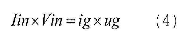
- Based on Equation (4), following Equation (5) is established.

- In the period in which the boosting operation is not performed by the
boost circuit 10, the voltage drop ΔV in theboost circuit 10 can be expressed as following Equation (6). In following Equation (6), "RL" denotes the resistance component of the reactor L1, and "RSW" denotes the ON resistance of the switching element Q6.
- Based on Equations (5) and (6) above, the voltage drop ΔV in the
boost circuit 10 can be expressed as following Equation (7).
- Because the bus voltage Vpn is a voltage resulting from adding the voltage drop ΔV to the power source voltage Vin, as indicated by following Equation (8), the bus voltage Vpn can be estimated from the power source voltage Vin and the voltage drop ΔV.

- The bus
voltage estimating unit 61 stores therein the resistance component RL of the reactor L1 and the ON resistance RSW of the switching element Q6 as parameters. The busvoltage estimating unit 61 estimates the voltage drop ΔV by performing the operation of Equation (7) using these parameters, and obtains the estimated bus voltage Vpn^ by adding the estimated voltage drop ΔV to the power source voltage Vin. -
FIG. 6 is a schematic illustrating an example of a configuration of the busvoltage estimating unit 61. As illustrated inFIG. 6 , the busvoltage estimating unit 61 includes a voltagedrop estimating unit 71 and anadder 72. The voltagedrop estimating unit 71 obtains an estimated voltage drop ΔV^ that is an estimation of the voltage drop ΔV by performing the operation of Equation (7) above based on the power source voltage Vin, the output voltage ug, and the output current ig. Theadder 72 obtains the estimated bus voltage Vpn^ by adding the estimated voltage drop ΔV^ to the power source voltage Vin. - The bus
voltage estimating unit 61 may also obtain the estimated voltage drop ΔV^ by performing the operation of Equation (6) above using the parameters mentioned above, and obtain the estimated bus voltage Vpn^ by adding the estimated voltage drop ΔV^ to the power source voltage Vin. - The replacing
unit 62 outputs the estimated bus voltage Vpn^ calculated by the busvoltage estimating unit 61 to thevoltage detection filter 22 as the delay compensating value Vcmp at the timing at which the switching signal Sw is switched from the High level to the Low level. In this manner, the output from thevoltage detection filter 22 is modified based on the estimated bus voltage Vpn^. - Let us assume herein that, as an example, the
voltage detection filter 22 is a first-order digital low-pass filter. In such a case, a relation between the bus voltage Vpn1 and the bus voltage Vpn2 that are respectively the input to and the output from thevoltage detection filter 22 can be expressed as following Equation (9).
- Discretizing Equation (9) above with s = (1 - Z-1)/ts, Equation (9) can be expressed as following Equation (10) .

- As one can see from Equation (10), assuming that the latest input voltage Vpn1(k) is equal to a previous output voltage Vpn2(k - 1), Vpn2(k) = Vpn2(k - 1) is established. The latest output voltage Vpn2(k), therefore, converges into the previous output voltage Vpn2(k - 1).
- As illustrated in
FIG. 3 , in the period in which the PWM operation is performed in the single-phase inverter 11, the bus voltage Vpn remains constant. After the switching signal Sw is switched from the High level to the Low level, therefore, the bus voltage Vpn1 output from thebus voltage detector 17 remains constant. - The replacing
unit 62 therefore replaces the previous output voltage Vpn2(k - 1) from thevoltage detection filter 22 with the delay compensating value Vcmp, at the timing at which the switching signal Sw is switched from the High level to the Low level. - In this manner, the bus voltage Vpn2 output from the
voltage detection filter 22 is modified as a voltage corresponding to the estimated bus voltage Vpn^, and theinverter controlling unit 23 can control the single-phase inverter 11 based on the bus voltage Vpn2 having corrected with the detection delay. It is therefore possible to suppress the distortion in the output voltage ug from the single-phase inverter 11, when the control is switched from the boosting operation in theboost circuit 10 to the PWM operation in the single-phase inverter 11. - The
voltage detection filter 22 is not limited to a first-order digital low-pass filter. For example, thevoltage detection filter 22 may be an n-th order digital low-pass filter (where n is an integer equal to or larger than two), or any other digital filter. - The replacing
unit 62 is explained to replace the previous output voltage Vpn2(k - 1) with the delay compensating value Vcmp, as an internal value of thevoltage detection filter 22, but the internal value used in the replacement is not limited to the previous output voltage Vpn2(k - 1). For example, the replacingunit 62 may have a function or a configuration for modifying any internal value of thevoltage detection filter 22, the internal value being capable of compensating the detection delay, based on the delay compensating value Vcmp. -
FIG. 7 is a flowchart of an example of the control process performed by thecontroller 20. Thecontroller 20 repeats the control process illustrated inFIG. 7 at a given cycle. - As illustrated in
FIG. 7 , thecontroller 20 generates the AC voltage reference Ug* (Step 10), and obtains the detected power source voltage Vin from the output voltage detector 16 (Step 11). - The
controller 20 then determines if the absolute value of the AC voltage reference Ug* is equal to or lower than the power source voltage Vin (Step 12). If the absolute value of the AC voltage reference Ug* is determined to be equal to or lower than the power source voltage Vin (Yes at Step 12), thecontroller 20 further determines if timing for compensating a delay has arrived (Step 13). - At the timing when the absolute value of the AC voltage reference Ug* switches from a value higher than the power source voltage Vin to a value equal to or lower than the power source voltage Vin, the
controller 20 determines that the timing for compensating a delay has arrived at Step 13. If thecontroller 20 determines that the timing for compensating a delay has arrived (Yes at Step 13), thecontroller 20 generates the delay compensating value Vcmp, and modifies the bus voltage Vpn2 based on the delay compensating value Vcmp (Step 14). - If the process at
Step 14 is completed, or if thecontroller 20 determines that the timing for compensating a delay has not arrived yet (No at Step 13), thecontroller 20 generates the gate signals S1 to S4 based on the bus voltage Vpn2 and the AC voltage reference Ug*, and performs the control for the PWM operation in the single-phase inverter 11 (Step 15). - If the
controller 20 determines that the absolute value of the AC voltage reference Ug* is not equal to or lower than the power source voltage Vin at Step 12 (No at Step 12), thecontroller 20 generates the gate signals S5 and S6 based on the AC voltage reference Ug*, and performs the control for the boosting operation in the boost circuit 10 (Step 16). - In the manner described above, the
power converter 2 according to the first embodiment modifies the output from thevoltage detection filter 22, based on the delay compensating value Vcmp for compensating the detection delay in thevoltage detection filter 22, at the timing at which the control is switched from the boosting operation in theboost circuit 10 to the PWM operation in the single-phase inverter 11. This configuration enables a distortion in the output voltage ug output from the single-phase inverter 11 to be suppressed even in a circuitry performing the control for the boosting operation in theboost circuit 10 and for the PWM-operation in the single-phase inverter 11 alternatingly so that the single-phase inverter 11 outputs an AC voltage. - A power converter in a power generating system according to a second embodiment will now be explained. The power generating system according to the second embodiment has the same configuration as that of the
power generating system 1 except for the configuration of the detected voltage modifying unit. Therefore, illustrations and explanations thereof are omitted herein, and the elements having the same function as those in thepower converter 2 are assigned with the same reference numerals, and redundant explanations thereof are omitted herein. -
FIG. 8 is a schematic illustrating a configuration of the detected voltage modifying unit according to the second embodiment. As illustrated inFIG. 8 , this detectedvoltage modifying unit 25A includes astorage unit 64 and a replacingunit 65. - The storage unit 64 (an example of a retaining unit) stores therein to retain the bus voltage Vpn2 output from the
voltage detection filter 22 immediately before the switching signal Sw is switched from the Low level to the High level, and outputs the stored bus voltage Vpn2 to the replacingunit 65 as the delay compensating value Vcmp. - The replacing
unit 65 replaces the previous output voltage Vpn2(k - 1) from thevoltage detection filter 22 with the delay compensating value Vcmp, at the timing at which the switching signal Sw is switched from the High level to the Low level. - Immediately before the switching signal Sw is switched from the Low level to the High level, the bus voltage Vpn is a stable DC voltage, and the bus voltage Vpn2 output from the
voltage detection filter 22 has noise removed by thevoltage detection filter 22. - Therefore, by replacing the previous output voltage Vpn2(k - 1) from the
voltage detection filter 22 with the delay compensating value Vcmp, using the bus voltage Vpn2 immediately before the switching signal Sw is switched from the Low level to the High level as the delay compensating value Vcmp, a distortion in the output voltage ug can be suppressed accurately. - In the period in which the bus voltage Vpn is a stable DC voltage, the bus voltage Vpn2 to be stored in the
storage unit 64 does not need to be the bus voltage Vpn2 immediately before the switching signal Sw is switched from the Low level to the High level. Thestorage unit 64 may store therein the bus voltage Vpn2 output from thevoltage detection filter 22 at the timing at which a predetermined period has elapsed from when the switching signal Sw is switched from the High level to the Low level, for example. The timing at which thestorage unit 64 stores therein the bus voltage Vpn2 can be specified as a parameter. - A power converter in a power generating system according to a third embodiment will now be explained. The power generating system according to the third embodiment has the same configuration as that of the
power generating system 1 except for the configuration of the detected voltage modifying unit. Therefore, illustrations and explanations thereof are omitted herein, and the elements having the same function as those in thepower converter 2 are assigned with the same reference numerals, and redundant explanations thereof are omitted herein. -
FIG. 9 is a schematic illustrating a configuration of the detected voltage modifying unit according to the third embodiment. As illustrated inFIG. 9 , this detectedvoltage modifying unit 25B includes the busvoltage estimating unit 61 and a replacingunit 62B. - If the switching signal Sw is set to the High level, the replacing
unit 62B outputs the bus voltage Vpn2 received from thevoltage detection filter 22 to theinverter controlling unit 23. In a period until a predetermined condition is satisfied from the timing at which the switching signal Sw is switched from the High level to the Low level, the replacingunit 62B outputs the estimated bus voltage Vpn^ estimated by the busvoltage estimating unit 61 to theinverter controlling unit 23 as the delay compensating value Vcmp. As a result, the output from thevoltage detection filter 22 is modified based on the estimated bus voltage Vpn^. - The period for which the replacing
unit 62B keeps outputting the delay compensating value Vcmp to theinverter controlling unit 23 is a predetermined period, and is set to a period equal to or longer than the period in which the bus voltage Vpn2 becomes substantially equal to the bus voltage Vpn, for example. Given such a condition, when the predetermined period elapses, the replacingunit 62B switches the output to theinverter controlling unit 23 from the delay compensating value Vcmp to the bus voltage Vpn2. - As another example, the period for which the replacing
unit 62B keeps outputting the delay compensating value Vcmp to theinverter controlling unit 23 may also be specified as a period until the amount of change in the output from thevoltage detection filter 22 becomes equal to or smaller than a predetermined amount. Given such a condition, the replacingunit 62B calculates the amount of change in the bus voltage Vpn2, for example, and switches the output to theinverter controlling unit 23 from the delay compensating value Vcmp to the bus voltage Vpn2 when the amount of change becomes equal to or smaller than the predetermined amount. - As another example, the period for which the replacing
unit 62B keeps outputting the delay compensating value Vcmp to theinverter controlling unit 23 may also be specified as a period until the difference between the bus voltage Vpn2 and the estimated bus voltage Vpn^ becomes equal to or smaller than a predetermined value. Given such a condition, the replacingunit 62B calculates the difference between the bus voltage Vpn2 and the estimated bus voltage Vpn^, for example, and switches the output to theinverter controlling unit 23 from the delay compensating value Vcmp to the bus voltage Vpn2 when the difference becomes equal to or smaller than the predetermined value. - In the manner described above, the power converter according to the third embodiment keeps the bus voltage Vpn2 replaced with the delay compensating value Vcmp for the period until a given condition is satisfied from when the control is switched from the boosting operation in the
boost circuit 10 to the PWM operation in the single-phase inverter 11. In this manner, the distortion in the output voltage ug can be suppressed. Thevoltage detection filter 22 is not limited to a digital filter. Thevoltage detection filter 22 may also be an analog low-pass filter, for example. - A power converter in a power generating system according to a fourth embodiment will now be explained. The power generating system according to the fourth embodiment has the same configuration as that of the
power generating system 1 except for the configuration of the detected voltage modifying unit. Therefore, illustrations and explanations thereof are omitted herein, and the elements having the same function as those in thepower converter 2 are assigned with the same reference numerals, and redundant explanations thereof are omitted herein. -
FIG. 10 is a schematic illustrating a configuration of the detected voltage modifying unit according to the fourth embodiment. As illustrated inFIG. 10 , this detectedvoltage modifying unit 25C includes aswitching determining unit 60, the busvoltage estimating unit 61, and a replacingunit 62C. - The
switching determining unit 60 outputs a High-level switching signal Sw1 when the difference between the bus voltage Vpn2 and the estimated bus voltage Vpn^ is equal to or smaller than a predetermined value, and outputs a Low-level switching signal Sw1 when the difference between the bus voltage Vpn2 and the estimated bus voltage Vpn^ is larger than the predetermined value. - If the switching signal Sw1 output from the
switching determining unit 60 is set to the High level, the replacingunit 62C outputs the bus voltage Vpn2 to theinverter controlling unit 23. If the switching signal Sw1 output from theswitching determining unit 60 is set to the Low level, the replacingunit 62C outputs the estimated bus voltage Vpn^ estimated by the busvoltage estimating unit 61 to theinverter controlling unit 23 as the delay compensating value Vcmp. - At the timing at which the control is switched from the boosting operation in the
boost circuit 10 to the PWM operation in the single-phase inverter 11, the difference between the bus voltage Vpn2 and the estimated bus voltage Vpn^ becomes larger than a predetermined value. Therefore, by causing the replacingunit 62C to replace the bus voltage Vpn2 with the delay compensating value Vcmp at the timing at which the control is switched from the boosting operation in theboost circuit 10 to the PWM operation in the single-phase inverter 11, the distortion in the output voltage ug can be suppressed. Thevoltage detection filter 22 is not limited to a digital filter.
Thevoltage detection filter 22 may also be an analog low-pass filter, for example. - A power converter in a power generating system according to a fifth embodiment will now be explained. The power generating system according to the fifth embodiment has the same configuration as that of the
power generating system 1 except for the configuration of the detected voltage modifying unit. Therefore, illustrations and explanations thereof are omitted herein, and the elements having the same function as those in thepower converter 2 are assigned with the same reference numerals, and redundant explanations thereof are omitted herein. -
FIG. 11 is a schematic illustrating a configuration of the detected voltage modifying unit according to the fifth embodiment. As illustrated inFIG. 11 , this detectedvoltage modifying unit 25D includes astorage unit 64D and a replacingunit 65D. - The
storage unit 64D (an example of the retaining unit) stores therein to retain the bus voltage Vpn2 output from thevoltage detection filter 22 immediately before the switching signal Sw is switched from the Low level to the High level. Thestorage unit 64D outputs the stored bus voltage Vpn2 to the replacingunit 65D as the delay compensating value Vcmp. - The replacing
unit 65D outputs the bus voltage Vpn2 received from thevoltage detection filter 22 to theinverter controlling unit 23 when the switching signal Sw is set to the High level. The replacingunit 65D outputs the delay compensating value Vcmp received from thestorage unit 64D to theinverter controlling unit 23 during the period until a predetermined condition is satisfied from the timing at which the switching signal Sw is switched from the High level to the Low level. "The period until a predetermined condition is satisfied" is the same as that in the detectedvoltage modifying unit 25C according to the third embodiment, for example. - In the manner described above, the power converter according to the fifth embodiment replaces the bus voltage Vpn2 with the delay compensating value Vcmp during the period until a given condition is satisfied from when the control is switched from the boosting operation in the
boost circuit 10 to the PWM operation in the single-phase inverter 11. In this manner, the distortion in the output voltage ug can be suppressed. Thevoltage detection filter 22 is not limited to a digital filter. Thevoltage detection filter 22 may also be an analog low-pass filter, for example. - A power converter according to a sixth embodiment will now be explained. The power converter according to the sixth embodiment has the same configuration as the power converter according to any one of the first to the fifth embodiment except for the configuration of the reference generating unit. Therefore, illustrations and explanations thereof are partially omitted, and the elements having the same function as those in the power converter according to the first to the fifth embodiments are assigned with the same reference numerals, and redundant explanations thereof are omitted herein. To the single-
phase inverter 11 in the power converter according to the sixth embodiment, an AC motor is connected, as another example, instead of the electrical grid 4. -
FIG. 12 is a schematic of a configuration of the reference generating unit according to the sixth embodiment. As illustrated inFIG. 12 , thisreference generating unit 21E includes aphase detector 30, theswitching determining unit 39, the switchingunit 40, an effective voltageamplitude calculating unit 81, a voltagereference output unit 82, asubtractor 83, and an ACvoltage reference generator 84. - The effective voltage
amplitude calculating unit 81 calculates the effective amplitude Ug of the output voltage ug. The effective voltageamplitude calculating unit 81 obtains the effective amplitude Ug of the output voltage ug by, for example, calculating the amplitude of the output voltage ug, and multiplying 1/√2 to the amplitude. - The voltage
reference output unit 82 outputs a voltage reference Ug1* to thesubtractor 83. Thesubtractor 83 calculates a deviation between the voltage reference Ug1* and the effective amplitude Ug of the output voltage ug, and outputs the deviation to the AC voltage reference generator. - The AC
voltage reference generator 84 generates the AC voltage reference Ug* in such a manner that the deviation between the voltage reference Ug1* and the effective amplitude Ug becomes zero. For example, the ACvoltage reference generator 84 includes, for example, a PI controller, and obtains the amplitude M of the AC voltage reference Ug* making the deviation between the voltage reference Ug1* and the effective amplitude Ug zero. The ACvoltage reference generator 84 generates the AC voltage reference Ug* (= M × sinθ) based on the amplitude M and the output voltage phase θ. The ACvoltage reference generator 84 outputs the generated AC voltage reference Ug* to theswitching unit 40 or to theswitching determining unit 39. - In the manner described above, the power converter according to the sixth embodiment can generate the AC voltage reference Ug* based on the voltage reference Ug1*, and is capable of operating autonomously. Therefore, even when an AC motor is connected to the single-
phase inverter 11, a power converter capable of suppressing the distortion in the output voltage ug can be provided. - In the first to the fifth embodiments described above, the process of generating the AC voltage reference Ug* can be performed easily because the voltage reference can be generated using scalar quantities of the d-axis component and the q-axis component. However, the AC voltage reference Ug* may also be generated using vector quantities only.
- Furthermore, explained in the embodiments described above is an example in which the control is switched between the boosting operation in the
boost circuit 10 and the PWM operation in the single-phase inverter 11 based on whether the absolute value of the AC voltage reference Ug* is equal to or lower than the power source voltage Vin. However, the condition for switching the control between the boosting operation in theboost circuit 10 and the PWM operation in the single-phase inverter 11 is not limited to the example described above. - For example, considering the voltage drop ΔV resulting from the resistance component of the reactor L1 and the ON resistance of the switching element Q6, the control may be switched between the boosting operation in the
boost circuit 10 and the PWM operation in the single-phase inverter 11 based on whether the AC voltage reference Ug* is equal to or lower than a predetermined voltage Vsw (< Vin). The predetermined voltage Vsw is, for example, Vin + ΔV. In the period in which Vsw1 (< Vin) < Ug* < Vsw2 (> Vin), the boosting operation in theboost circuit 10 and the PWM operation in the single-phase inverter 11 may be performed simultaneously. - In the embodiments described above, the
bus voltage detector 17 is explained to detect the instantaneous value of the bus voltage Vpn, but thebus voltage detector 17 may also use a voltage divider to step-down the bus voltage Vpn at a predetermined ratio, and output the resultant voltage, for example. Given such a detector, thevoltage detection filter 22 converts the voltage output from thebus voltage detector 17 into a digital signal using an analog-to-digital (A/D) converter, and removes the noise from the digital signal with a filter. - Furthermore, in the embodiments described above, the switching elements Q1 to Q4, the switching elements Q5 and Q6, or both sets are made of a wide-bandgap semiconductor containing gallium nitride (GaN) or silicon carbide (SiC). Therefore, changes in the grid impedance or in the load connected to the output of the
power converter 2 can be actively compensated. - In the embodiments described above, the
voltage detection filter 17 is used as an example of means for processing (hereinafter, referred to as processing means) the detection result from thebus voltage detector 17. However, the processing means is not limited to thevoltage detection filter 17, and may be any means for processing the detection result and introducing a delay. Furthermore, in the embodiments described above, the detectedvoltage modifying units voltage modifying units
Claims (11)
- A power converter (2) comprising:a boost circuit (10) that boosts a voltage of a direct-current (DC) power source (3);a single-phase inverter (11) that converts a voltage output from the boost circuit (10) into an alternating-current (AC) voltage; anda controller (20) that switches between a boosting operation in the boost circuit (10) and a pulse-width modulation (PWM) operation in the single-phase inverter (11),the controller (20) includes:a voltage detection filter (22) that removes a noise component from a detection result of a voltage detector (17) detecting the output voltage of the boost circuit (10); anda detected voltage modifying unit (25, 25A, 25B, 25C, 25D) that modifies an output from the voltage detection filter (22) based on a delay compensating value for compensating a detection delay introduced by the voltage detection filter (22), when switching is performed from the boosting operation in the boost circuit (10) to the PWM operation in the single-phase inverter (11).
- The power converter (2) according to claim 1, wherein the controller (20) further includes:a reference generating unit (21, 21E) that generates an AC voltage reference for an AC voltage output from the single-phase inverter (11) to a load (4);a boosting controlling unit (24) that performs, when an absolute value of the AC voltage reference is higher than the voltage of the DC power source (3), control for the boosting operation in the boost circuit (10) to generate a first portion of the AC voltage, the first portion corresponding to the AC voltage reference of which the absolute value is higher than the voltage of the DC power source (3); andan inverter controlling unit (23) that performs, when the absolute value of the AC voltage reference is lower than the voltage of the DC power source (3), control for the PWM operation in the single-phase inverter (11) to generate a second portion of the AC voltage based on the output of the voltage detection filter (22) and the AC voltage reference, the second portion corresponding to the AC voltage reference of which the absolute value is lower than the voltage of the DC power source (3).
- The power converter (2) according to claim 1 or 2, wherein the detected voltage modifying unit (25, 25B, 25C) includes:an estimating unit (61) that estimates the output voltage of the boost circuit (10) as the delay compensating value; anda replacing unit (62, 62B, 62C) that replaces the output of the voltage detection filter (22) or an internal value of the voltage detection filter (22) with the delay compensating value, when switching is performed from the boosting operation in the boost circuit (10) to the PWM operation in the single-phase inverter (11).
- The power converter (2) according to claim 3, wherein the estimating unit (61) estimates the output voltage of the boost circuit (10) based on a voltage and a current output from the single-phase inverter (11), and the voltage of the DC power source (3).
- The power converter (2) according to claim 1 or 2, wherein the detected voltage modifying unit (25A, 25D) includes:a storage unit (64, 64D) that stores, as the delay compensating value, an output from the voltage detection filter (22) before switching is performed from the PWM operation in the single-phase inverter (11) to the boosting operation in the boost circuit (10) ; anda replacing unit (65, 65D) that replaces the output of the voltage detection filter (22) or an internal value of the voltage detection filter (22) with the delay compensating value stored in the storage unit (64, 64D), when switching is performed from the boosting operation in the boost circuit (10) to the PWM operation in the single-phase inverter (11).
- The power converter (2) according to any one of claims 3 to 5, wherein
the voltage detection filter (22) is a digital filter that removes a noise component from a detection result of the voltage detector (17) based on the detection result of the voltage detector (17) and a previous output from the voltage detection filter (22), and
the replacing unit (62, 62B, 62C, 65, 65D) replaces the previous output with the delay compensating value to modify the output of the voltage detection filter (22). - The power converter (2) according to any one of claims 3 to 5, wherein the replacing unit (62, 62B, 62C, 65, 65D) continuously replaces the output of the voltage detection filter (22) with the delay compensating value until an amount of change of the output from the voltage detection filter (22) becomes equal to or smaller than a predetermined amount, or until a predetermined period elapses from when switching is performed from the boosting operation in the boost circuit (10) to the PWM operation in the single-phase inverter (11).
- The power converter (2) according to any one of claims 1 to 7, wherein one set of switching elements (Q5, Q6) of the boost circuit (10), one set of switching elements (Q1 to Q4) of the single-phase inverter (11), or both the sets are made of a wide-bandgap semiconductor containing gallium nitride (GaN) or silicon carbide (SiC).
- A power generating system (1) comprising:the power converter (2) according to any one of claims 1 to 8; anda power generator (3) that supplies DC power to the power converter (2).
- An apparatus (20) for controlling a power converter (2), the apparatus (20) comprising:a voltage detection filter (22) that removes a noise component from a detection result of a voltage at a connection point between a boost circuit (10) boosting a voltage of a direct-current (DC) power source (3) and a single-phase inverter (11) converting a voltage output from the boost circuit (10) into an alternating-current (AC) voltage; anda detected voltage modifying unit (25, 25A, 25B, 25C, 25D) that modifies an output from the voltage detection filter (22) based on a delay compensating value for compensating a detection delay introduced by the voltage detection filter (22), when switching is performed from a boosting operation in the boost circuit (10) to a pulse-width modulation (PWM) operation in the single-phase inverter (11).
- A method for controlling a power converter (2), the method comprising:detecting a voltage at a connection point between a boost circuit (10) and a single-phase inverter (11), the boost circuit (10) boosting a voltage of a direct-current (DC) power source (3) and the single-phase inverter (11) converting a voltage output from the boost circuit (10) into an alternating-current (AC) voltage;removing a noise component from the detected voltage with a voltage detection filter (22); andmodifying an output from the voltage detection filter (22) based on a delay compensating value for compensating a detection delay introduced by the voltage detection filter (22), when switching is performed from a boosting operation in the boost circuit (10) to a pulse-width modulation (PWM) operation in the single-phase inverter (11).
Applications Claiming Priority (1)
| Application Number | Priority Date | Filing Date | Title |
|---|---|---|---|
| JP2014055400A JP6086085B2 (en) | 2014-03-18 | 2014-03-18 | Power conversion device, power generation system, control device for power conversion device, and control method for power conversion device |
Publications (1)
| Publication Number | Publication Date |
|---|---|
| EP2922192A1 true EP2922192A1 (en) | 2015-09-23 |
Family
ID=52394183
Family Applications (1)
| Application Number | Title | Priority Date | Filing Date |
|---|---|---|---|
| EP15152604.3A Withdrawn EP2922192A1 (en) | 2014-03-18 | 2015-01-27 | Power converter, power generating system, apparatus for controlling power converter, and method for controlling power converter |
Country Status (4)
| Country | Link |
|---|---|
| US (1) | US9484839B2 (en) |
| EP (1) | EP2922192A1 (en) |
| JP (1) | JP6086085B2 (en) |
| CN (1) | CN104935200A (en) |
Cited By (4)
| Publication number | Priority date | Publication date | Assignee | Title |
|---|---|---|---|---|
| EP3065285A1 (en) * | 2015-03-06 | 2016-09-07 | Sumitomo Electric Industries, Ltd. | Reversible dc-ac converter |
| EP3407479A4 (en) * | 2016-01-18 | 2019-09-11 | Sumitomo Electric Industries, Ltd. | POWER CONVERSION SYSTEM AND ITS CONTROL METHOD |
| AT521314A1 (en) * | 2018-08-23 | 2019-12-15 | Avl List Gmbh | Fuel cell system and method for voltage regulation in the fuel cell system |
| EP4175164A1 (en) * | 2021-10-28 | 2023-05-03 | Carrier Corporation | Boost converter state control |
Families Citing this family (24)
| Publication number | Priority date | Publication date | Assignee | Title |
|---|---|---|---|---|
| US9742286B2 (en) * | 2011-06-08 | 2017-08-22 | L-3 Communications Magnet-Motor Gmbh | Method of controlling a DC/AC converter |
| WO2014192373A1 (en) * | 2013-05-27 | 2014-12-04 | 株式会社東芝 | Power conversion device, power conversion device control method, rotation sensorless control device, and rotation sensorless control device control method |
| TW201513541A (en) * | 2013-09-26 | 2015-04-01 | 台達電子工業股份有限公司 | Micro inverter of solar power generation system and operation method thereof |
| JP6485251B2 (en) * | 2015-06-29 | 2019-03-20 | 住友電気工業株式会社 | Conversion device and control method thereof |
| JP6419977B2 (en) * | 2015-09-03 | 2018-11-14 | 株式会社東芝 | Voltage fluctuation suppressing apparatus and method |
| JP6601125B2 (en) * | 2015-10-07 | 2019-11-06 | 住友電気工業株式会社 | Power conversion apparatus and control method thereof |
| US10749348B2 (en) * | 2015-10-28 | 2020-08-18 | Kyocera Corporation | Power control apparatus, control method for power control apparatus, power control system, and control method for power control system |
| JP6776695B2 (en) * | 2016-07-26 | 2020-10-28 | 株式会社明電舎 | Power converter |
| JP6952245B2 (en) * | 2016-09-30 | 2021-10-20 | パナソニックIpマネジメント株式会社 | Power conversion system |
| US10153691B2 (en) * | 2016-10-07 | 2018-12-11 | Laszlo Keszthelyi | Photovoltaic panel power output booster and method |
| KR101904101B1 (en) * | 2016-12-26 | 2018-10-05 | 효성중공업 주식회사 | Method for removing DC component of MMC converter output |
| US12225657B2 (en) * | 2017-01-03 | 2025-02-11 | Transportation Ip Holdings, Llc | Power system and method for controlling power modules |
| US20180191336A1 (en) * | 2017-01-03 | 2018-07-05 | General Electric Company | Systems and methods for power modules |
| US12249925B2 (en) * | 2017-06-23 | 2025-03-11 | En2Core Technology, Inc. | Power supply and method of supplying power to load |
| KR102012743B1 (en) | 2017-06-23 | 2019-08-21 | 인투코어테크놀로지 주식회사 | Power supply supporting device and method of supporting power supply to load |
| CN109387701B (en) * | 2017-08-02 | 2021-03-19 | 台达电子工业股份有限公司 | Three-phase converter device and capacitance estimation method |
| CN109494706A (en) * | 2017-09-11 | 2019-03-19 | 台达电子工业股份有限公司 | Integrated power supply system |
| JP7086741B2 (en) * | 2018-06-18 | 2022-06-20 | 新電元工業株式会社 | Grid interconnection inverter device and stabilization control method |
| US20200148064A1 (en) * | 2018-11-13 | 2020-05-14 | Ford Global Technologies, Llc | Power supply device |
| EP4029139A4 (en) * | 2019-09-13 | 2023-09-27 | Milwaukee Electric Tool Corporation | Power converters with wide bandgap semiconductors |
| CN114764259A (en) * | 2021-01-11 | 2022-07-19 | 台达电子企业管理(上海)有限公司 | Current control device and power conversion system using the same |
| CN112366970B (en) * | 2021-01-14 | 2021-04-02 | 深圳市正浩创新科技有限公司 | Inversion system, inversion system control method and parallel inversion system |
| JP7439003B2 (en) * | 2021-02-24 | 2024-02-27 | 日立Astemo株式会社 | Inverter control device, electric vehicle system |
| CN114865709B (en) * | 2022-07-07 | 2022-09-30 | 浙江日风电气股份有限公司 | Bus voltage control method, device and medium for single-phase photovoltaic inverter |
Citations (3)
| Publication number | Priority date | Publication date | Assignee | Title |
|---|---|---|---|---|
| JP2000152661A (en) * | 1998-11-10 | 2000-05-30 | Matsushita Electric Ind Co Ltd | Grid-connected inverter device |
| US20120201064A1 (en) * | 2011-02-03 | 2012-08-09 | Denso Corporation | Power converter |
| WO2013069326A1 (en) | 2011-11-07 | 2013-05-16 | 三菱電機株式会社 | Electrical power conversion device |
Family Cites Families (11)
| Publication number | Priority date | Publication date | Assignee | Title |
|---|---|---|---|---|
| JP4195948B2 (en) * | 1998-11-05 | 2008-12-17 | パナソニック株式会社 | Grid interconnection inverter |
| US7221121B2 (en) * | 2001-11-23 | 2007-05-22 | Danfoss Drives A/S | Frequency converter for different mains voltages |
| CN101529709B (en) * | 2006-10-19 | 2012-06-27 | 三菱电机株式会社 | Power conversion device |
| MX2010008059A (en) * | 2008-02-13 | 2010-08-18 | Mitsubishi Electric Corp | Power converting device. |
| JP2010250728A (en) * | 2009-04-20 | 2010-11-04 | Panasonic Corp | Inverter device |
| DE112010002360T5 (en) * | 2009-06-09 | 2012-08-30 | Honda Motor Co., Ltd. | Control device for load drive system |
| JP2011036040A (en) * | 2009-07-31 | 2011-02-17 | Renesas Electronics Corp | System interconnection system and system interconnection method |
| JP5178670B2 (en) * | 2009-09-17 | 2013-04-10 | 三菱電機株式会社 | Power converter |
| JPWO2011090210A1 (en) * | 2010-01-25 | 2013-05-23 | 三洋電機株式会社 | Power conversion device, grid interconnection device, and grid interconnection system |
| US8767421B2 (en) * | 2011-06-16 | 2014-07-01 | Solarbridge Technologies, Inc. | Power converter bus control method, system, and article of manufacture |
| JP5880289B2 (en) * | 2012-05-31 | 2016-03-08 | 三菱電機株式会社 | Power converter |
-
2014
- 2014-03-18 JP JP2014055400A patent/JP6086085B2/en active Active
-
2015
- 2015-01-27 EP EP15152604.3A patent/EP2922192A1/en not_active Withdrawn
- 2015-01-29 US US14/608,190 patent/US9484839B2/en active Active
- 2015-03-12 CN CN201510110083.4A patent/CN104935200A/en active Pending
Patent Citations (3)
| Publication number | Priority date | Publication date | Assignee | Title |
|---|---|---|---|---|
| JP2000152661A (en) * | 1998-11-10 | 2000-05-30 | Matsushita Electric Ind Co Ltd | Grid-connected inverter device |
| US20120201064A1 (en) * | 2011-02-03 | 2012-08-09 | Denso Corporation | Power converter |
| WO2013069326A1 (en) | 2011-11-07 | 2013-05-16 | 三菱電機株式会社 | Electrical power conversion device |
Non-Patent Citations (1)
| Title |
|---|
| AHMED N A ET AL: "Dual-mode time-sharing one-stage single-phase power conditioner using sinewave tracked soft switching PWM boost chopper", CONFERENCE RECORD OF THE 2005 IEEE INDUSTRY APPLICATIONS CONFERENCE FORTIETH IAS ANNUAL MEETING 2-6 OCT. 2005 KOWLOON, HONG KONG, CHINA, IEEE, CONFERENCE RECORD OF THE 2005 IEEE INDUSTRY APPLICATIONS CONFERENCE FORTIETH IAS ANNUAL MEETING (IEEE CAT., vol. 3, 2 October 2005 (2005-10-02), pages 1612 - 1617, XP010842610, ISBN: 978-0-7803-9208-3, DOI: 10.1109/IAS.2005.1518662 * |
Cited By (10)
| Publication number | Priority date | Publication date | Assignee | Title |
|---|---|---|---|---|
| EP3065285A1 (en) * | 2015-03-06 | 2016-09-07 | Sumitomo Electric Industries, Ltd. | Reversible dc-ac converter |
| CN105939128A (en) * | 2015-03-06 | 2016-09-14 | 住友电气工业株式会社 | Conversion device |
| US9800177B2 (en) | 2015-03-06 | 2017-10-24 | Sumitomo Electric Industries, Ltd. | Conversion device |
| CN105939128B (en) * | 2015-03-06 | 2020-07-03 | 住友电气工业株式会社 | Conversion device |
| EP3407479A4 (en) * | 2016-01-18 | 2019-09-11 | Sumitomo Electric Industries, Ltd. | POWER CONVERSION SYSTEM AND ITS CONTROL METHOD |
| TWI701898B (en) * | 2016-01-18 | 2020-08-11 | 日商住友電氣工業股份有限公司 | Power conversion system and its control method |
| US11139657B2 (en) | 2016-01-18 | 2021-10-05 | Sumitomo Electric Industries, Ltd. | Power conversion system and control method therefor |
| AT521314A1 (en) * | 2018-08-23 | 2019-12-15 | Avl List Gmbh | Fuel cell system and method for voltage regulation in the fuel cell system |
| EP4175164A1 (en) * | 2021-10-28 | 2023-05-03 | Carrier Corporation | Boost converter state control |
| US12328080B2 (en) | 2021-10-28 | 2025-06-10 | Carrier Corporation | Boost converter state control |
Also Published As
| Publication number | Publication date |
|---|---|
| US9484839B2 (en) | 2016-11-01 |
| US20150270787A1 (en) | 2015-09-24 |
| CN104935200A (en) | 2015-09-23 |
| JP6086085B2 (en) | 2017-03-01 |
| JP2015180120A (en) | 2015-10-08 |
Similar Documents
| Publication | Publication Date | Title |
|---|---|---|
| US9484839B2 (en) | Power converter, power generating system, apparatus for controlling power converter, and method for controlling power converter | |
| US9509229B2 (en) | Power supply apparatus including power conversion circuit controlled by PWM control circuit | |
| US10666163B2 (en) | Electric-power conversion apparatus | |
| US9509233B2 (en) | Power converter, power generation system, control apparatus, and power conversion method | |
| EP2408100B1 (en) | Power conversion device, and method for controlling thereof | |
| US9013906B2 (en) | Power system-interconnected inverter device | |
| EP1921740B1 (en) | Power converter control | |
| US10541638B2 (en) | Control apparatus and control method | |
| JP6103155B2 (en) | Power converter, power generation system, and current control method | |
| US10411615B2 (en) | Power converter | |
| JP6399239B2 (en) | Power converter | |
| KR20120139517A (en) | Control device of ac motor and refrigerating air conditioner using the same | |
| US20150188454A1 (en) | Inverter device, control circuit for inverter device, and method for controlling inverter device | |
| EP3316471B1 (en) | Conversion device and method for controlling the same | |
| KR101848265B1 (en) | System and Method for Controlling Grid Connected Inverter Using Disturbance Observer | |
| US10666131B2 (en) | Dead-time voltage compensation apparatus and dead-time voltage compensation method | |
| JP2004201440A (en) | Pulse width modulation method and apparatus, power conversion method and power converter | |
| Somkun et al. | Fast DC bus voltage control of single-phase PWM rectifiers using a ripple voltage estimator | |
| Kukkola et al. | A voltage-sensorless controller for grid converters | |
| JP6837576B2 (en) | Power converter | |
| CN103930844B (en) | For correcting control method and the system of the voltage of electric loading to be put on | |
| JP2020115719A (en) | Power control method and power controller | |
| EP3471258A1 (en) | Power converter | |
| JP2007006700A (en) | Power converter |
Legal Events
| Date | Code | Title | Description |
|---|---|---|---|
| PUAI | Public reference made under article 153(3) epc to a published international application that has entered the european phase |
Free format text: ORIGINAL CODE: 0009012 |
|
| AK | Designated contracting states |
Kind code of ref document: A1 Designated state(s): AL AT BE BG CH CY CZ DE DK EE ES FI FR GB GR HR HU IE IS IT LI LT LU LV MC MK MT NL NO PL PT RO RS SE SI SK SM TR |
|
| AX | Request for extension of the european patent |
Extension state: BA ME |
|
| 17P | Request for examination filed |
Effective date: 20160323 |
|
| RBV | Designated contracting states (corrected) |
Designated state(s): AL AT BE BG CH CY CZ DE DK EE ES FI FR GB GR HR HU IE IS IT LI LT LU LV MC MK MT NL NO PL PT RO RS SE SI SK SM TR |
|
| STAA | Information on the status of an ep patent application or granted ep patent |
Free format text: STATUS: THE APPLICATION HAS BEEN WITHDRAWN |
|
| 18W | Application withdrawn |
Effective date: 20160718 |