EP1921740B1 - Power converter control - Google Patents
Power converter control Download PDFInfo
- Publication number
- EP1921740B1 EP1921740B1 EP07119903.8A EP07119903A EP1921740B1 EP 1921740 B1 EP1921740 B1 EP 1921740B1 EP 07119903 A EP07119903 A EP 07119903A EP 1921740 B1 EP1921740 B1 EP 1921740B1
- Authority
- EP
- European Patent Office
- Prior art keywords
- carrier wave
- voltage
- frequency
- command value
- dead
- Prior art date
- Legal status (The legal status is an assumption and is not a legal conclusion. Google has not performed a legal analysis and makes no representation as to the accuracy of the status listed.)
- Active
Links
- 230000008859 change Effects 0.000 claims description 60
- 230000001360 synchronised effect Effects 0.000 claims description 29
- 238000000034 method Methods 0.000 claims description 11
- 230000002265 prevention Effects 0.000 claims description 11
- 230000004044 response Effects 0.000 claims description 6
- 230000000737 periodic effect Effects 0.000 claims description 3
- 230000002123 temporal effect Effects 0.000 description 25
- 238000010586 diagram Methods 0.000 description 8
- 230000001747 exhibiting effect Effects 0.000 description 4
- 230000003595 spectral effect Effects 0.000 description 4
- 238000006243 chemical reaction Methods 0.000 description 2
- 230000006870 function Effects 0.000 description 2
- 230000002401 inhibitory effect Effects 0.000 description 2
- 239000003990 capacitor Substances 0.000 description 1
- 230000003111 delayed effect Effects 0.000 description 1
- 238000005516 engineering process Methods 0.000 description 1
- 238000012986 modification Methods 0.000 description 1
- 230000004048 modification Effects 0.000 description 1
- 239000004065 semiconductor Substances 0.000 description 1
Images


Classifications
-
- H—ELECTRICITY
- H02—GENERATION; CONVERSION OR DISTRIBUTION OF ELECTRIC POWER
- H02P—CONTROL OR REGULATION OF ELECTRIC MOTORS, ELECTRIC GENERATORS OR DYNAMO-ELECTRIC CONVERTERS; CONTROLLING TRANSFORMERS, REACTORS OR CHOKE COILS
- H02P6/00—Arrangements for controlling synchronous motors or other dynamo-electric motors using electronic commutation dependent on the rotor position; Electronic commutators therefor
- H02P6/14—Electronic commutators
-
- H—ELECTRICITY
- H02—GENERATION; CONVERSION OR DISTRIBUTION OF ELECTRIC POWER
- H02M—APPARATUS FOR CONVERSION BETWEEN AC AND AC, BETWEEN AC AND DC, OR BETWEEN DC AND DC, AND FOR USE WITH MAINS OR SIMILAR POWER SUPPLY SYSTEMS; CONVERSION OF DC OR AC INPUT POWER INTO SURGE OUTPUT POWER; CONTROL OR REGULATION THEREOF
- H02M7/00—Conversion of ac power input into dc power output; Conversion of dc power input into ac power output
- H02M7/42—Conversion of dc power input into ac power output without possibility of reversal
- H02M7/44—Conversion of dc power input into ac power output without possibility of reversal by static converters
- H02M7/48—Conversion of dc power input into ac power output without possibility of reversal by static converters using discharge tubes with control electrode or semiconductor devices with control electrode
Definitions
- the invention relates generally to power converter control and particularly, but not exclusively, to power converter control for converting an output from a direct current (DC) power supply into alternating current (AC) power and for supplying the converted AC power to loads.
- DC direct current
- AC alternating current
- aspects of the invention relate to an apparatus, to a control unit and to a method.
- the base unit of a power converter for converting DC power into three-phase AC power is an arm including series-connected upper and lower switching devices, and the upper and lower switching devices are alternately turned ON and OFF.
- a short-circuit prevention time (also referred to as a "dead time") for which the upper and lower switching devices are simultaneously turned OFF when they are switched from the ON state to the OFF state and vice versa is provided.
- an error may occur between a voltage command value output from a control unit and an actual output voltage (hereinafter such an error is referred to as an "error voltage"), which may cause distortion in the output voltage.
- an error voltage which is a constant value, is added to a voltage command value so that an error voltage can be compensated for.
- JP 2006-217776 A discloses a PWM inverter and it's control method, whereby a carrier frequency is changed over time so as to form a periodic waveform, whereby the carrier frequency and a control frequency become an arbitrary ratio, and whereby an electric current command is corrected according to the carrier frequency using dead-time correction within the current control means.
- Embodiments of the invention provide a power control unit and method wherein a command value is compensated in response to a change in the frequency of a carrier wave so that output fluctuations caused by error voltages can be suppressed.
- a power converter control unit for a power converter including an inverter configured to convert a direct current voltage into an alternating current voltage by controlling switching devices to be turned ON or OFF based on a control signal and to output the alternating current voltage to a load, the control unit comprising a command value output unit configured to output the command value, a carrier wave output unit configured to output a carrier wave, a frequency changing unit configured to change a frequency of the carrier wave, a compensator configured to compensate the command value in accordance with a change in the frequency of the carrier wave changed by the frequency changing unit and to output a command value signal and a control signal generator configured to compare the command value signal with the carrier wave and to generate the control signal based on a comparison result.
- the compensator is further configured to compensate the command value in synchronization with a change in the frequency of the carrier wave.
- the command value signal indicates a voltage and the compensator comprises a compensated voltage generator configured to generate a compensated voltage having a constant value to compensate the command value, a carrier wave corrected voltage generator configured to generate a carrier wave corrected voltage in response to the change in the frequency of the carrier wave and an adder configured to add the compensated voltage to the carrier wave corrected voltage to generate a compensation corrected voltage as the command value signal.
- the carrier wave corrected voltage generator is further configured to synchronize the carrier wave corrected voltage with a change in the frequency of the carrier wave.
- the command value signal output from the compensator indicates a voltage
- the compensator comprises a compensated voltage generator configured to generate a compensated voltage having a constant value to compensate the command value, a carrier wave corrected voltage generator configured to generate a carrier wave corrected voltage in response to the change in the frequency of the carrier wave and an adder configured to add the compensated voltage to the carrier wave corrected voltage to generate a compensation corrected voltage as the command value signal.
- the carrier wave corrected voltage generator is further configured to synchronize the carrier wave corrected voltage with a change in the frequency of the carrier wave.
- ⁇ Td ⁇ Vdc , or ⁇ ⁇ V t
- the load is a synchronous motor and the compensator is further configured to compensate a q-axis voltage of the synchronous motor
- the power converter further comprising a position detector configured to detect a position of a magnetic pole of the synchronous motor and a coordinate transformer configured to transform coordinates between a two-phase value and a three-phase value of the synchronous motor based on the position of the magnetic pole.
- ⁇ Td ⁇ Vdc , or ⁇ ⁇ Vq t ⁇ 3 / 2 ⁇
- the frequency changing unit is further configured to change the frequency of the carrier wave in a constant cycle.
- the control unit may comprise a current detector configured to detect a current from the inverter and a current polarity determination unit configured to determine a polarity of the current, wherein the compensator is further configured to compensate the command value in accordance with the change in the frequency of the carrier wave and the polarity of the current.
- the compensator is further configured to compensate the command value using a carrier wave corrected voltage wherein the carrier wave corrected voltage, when the polarity is positive, changes at a same rate as a rate of the change of the frequency of the carrier wave; and the carrier wave corrected voltage, when the polarity is negative, changes at a rate whose numerical value is the same as a rate of the change of the frequency of the carrier wave and whose sign is opposite to a sign of the carrier wave.
- a power converter control unit for a power converter, the power converter including an inverter configured to convert a direct current voltage into an alternating current voltage by controlling switching devices to be turned ON or OFF based on a control signal to supply the alternating current voltage to a load, the control unit comprising means for outputting a command value, means for outputting a carrier wave, means for changing a frequency of the carrier wave, means for compensating the command value in accordance with a change in the frequency of the carrier wave and for outputting a command value signal and means for comparing the command value signal with the carrier wave to generate the control signal.
- a power conversion method for a power converter comprising comparing a frequency of a carrier wave changing over time with a command value compensated in accordance with a change in the frequency of the carrier wave, converting a direct current voltage into an alternating current voltage by controlling switching devices to be turned ON and OFF based on a control signal generated based on a result of the comparing and outputting the alternative current voltage.
- the method may comprise compensating the command value in synchronization with the change in the frequency of the carrier wave.
- the method comprises changing the frequency of the carrier wave in a constant cycle.
- a power converter may include an inverter configured to convert a direct current voltage into an alternating current voltage by controlling switching devices to be turned ON or OFF based on a control signal and to output the alternating current voltage to a load
- a power converter control unit comprises a command value output unit configured to output the command value, a carrier wave output unit configured to output a carrier wave, a frequency changing unit configured to change a frequency of the carrier wave, a compensator configured to compensate the command value in accordance with a change in the frequency of the carrier wave changed by the frequency changing unit and to output a command value signal and a control signal generator configured to compare the command value signal with the carrier wave and to generate the control signal based on a comparison result.
- a control unit may comprise means for outputting a command value, means for outputting a carrier wave, means for changing a frequency of the carrier wave, means for compensating the command value in accordance with a change in the frequency of the carrier wave and for outputting a command value signal and means for comparing the command value signal with the carrier wave to generate the control signal.
- a power conversion method may comprise comparing a frequency of a carrier wave changing over time with a command value compensated in accordance with a change in the frequency of the carrier wave, converting a direct current voltage into an alternating current voltage by controlling switching devices to be turned ON and OFF based on a control signal generated based on a result of the comparing, and outputting the alternative current voltage.
- a power converter configured in accordance with a first embodiment of the invention is described below with reference to FIGS. 1 through 10 .
- the power converter shown in FIG. 1 includes a DC-power chargeable/dischargeable battery (DC power) 1, an inverter 2 that converts DC power stored in the battery 1 into AC power and outputs the converted AC power to a motor 6, a current detector 3 that detects an output current I of the AC power output from the inverter 2 to the motor 6 as a detected current value, and a control unit 4 that controls the inverter 2 based on the detected current value detected by the current detector 3 and a current command value output from a current command generator 5.
- DC power DC-power chargeable/dischargeable battery
- control unit 4 and the current command generator 5 are separately shown, they may be integrated into one controller. In FIG. 1 , they are shown as different elements for the sake of description.
- control unit 4 and/or the current command generator 5 can be, for example, a microcomputer including a random access memory (RAM), a read-only memory (ROM) and a central processing unit (CPU) in addition to various input and output connections.
- RAM random access memory
- ROM read-only memory
- CPU central processing unit
- the functions described herein for these components are performed by execution by the CPU of one or more programs stored in ROM.
- the parts of the control unit 4 and current command generator 5 shown in the figures and described below represent functional components of the one or more programs. Of course, some or all of the functions described can also be implemented in whole or in part by hardware.
- the inverter 2 includes six transistors Tu+, Tu-, Tv+, Tv-, Tw+ and Tw- and six diodes, each diode and the corresponding transistor forming a parallel circuit.
- the transistors Tu+, Tu-, Tv+, Tv-, Tw+ and Tw- are formed by semiconductor devices, such as insulated gate bipolar transistors (IGBTs).
- the current detector 3 includes three current sensors 3a, 3b and 3c that detect output currents Iu, Iv and Iw having u, v and w phases, respectively, output from the inverter 2 as detected current values.
- the current detector 3 outputs the detected current values to the control unit 4.
- the current sensors 3a, 3b and 3c are hereinafter simply referred to as the "current detector 3" unless they have to be distinguished from each other.
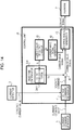
- the control unit 4 includes, as shown in FIG. 3 , the following elements.
- a voltage command generator 41 generates a voltage command based on a current command value output from the current command generator 5 and a detected current value output from the current detector 3.
- a carrier wave signal generator 42 generates a carrier wave signal.
- a dead-time compensator 44 outputs a dead-time compensation corrected voltage ⁇ V, which is described below.
- An adder 46 adds the dead-time compensation corrected voltage ⁇ V to the voltage command to generate a command value signal.
- a control signal generator 43 compares (e.g., using PWM comparison) the command value signal with the carrier wave signal and generates a control signal for turning ON or OFF the transistors of the inverter 2.
- a carrier wave frequency changer 45 changes the frequency fc of the carrier wave signal.
- the carrier wave signal generator 42 performs frequency modulation on the carrier wave signal on the basis of the carrier wave frequency fc output from the carrier wave frequency changer 45 and outputs the resulting carrier wave signal.
- the control signal generator 43 compares the command value signal output from the adder 46 with the carrier wave signal by the use of a comparator to generate a pulsating control signal. The control signal generator 43 then outputs this control signal to the inverter 2.
- the dead-time compensator 44 includes, as shown in FIG. 4 , the following elements.
- a dead-time compensated voltage generator 441 generates a dead-time compensated voltage ⁇ V1, which is a constant voltage.
- a carrier wave corrected voltage generator 442 generates a carrier wave corrected voltage ⁇ V2 in synchronization with the carrier wave frequency fc output from the carrier wave frequency changer 45. That is, the frequency of the carrier wave corrected voltage ⁇ V2 and that of the carrier wave frequency fc coincide.
- An adder 443 adds the carrier wave corrected voltage ⁇ V2 to the dead-time compensated voltage ⁇ V1 and outputs the resulting dead-time compensation corrected voltage ⁇ V to the adder 46.
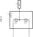
- FIG. 5 illustrates the inverter 2 in a simplified form.
- the battery 1 supplies the DC voltages V+ and V- to the inverter 2.
- a control signal generated by the control signal generator 43 (see FIG. 3 ) is input into the gate terminals of the transistors Tu+ and Tu-.
- the control signal is an ON/OFF pulse signal generated by the control signal generator 43 based on a result of comparing (e.g., by PWM comparison) the command value signal with the carrier wave signal by the control signal generator 43. Based on this control signal, the transistors Tu+ and Tu- are turned ON or OFF to allow power to be supplied from the inverter 2 to the motor 6.
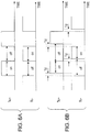
- FIGS. 6A and 6B are time charts illustrating control signals input into the gate terminals of the transistors Tu+ and Tu- shown in FIG. 5 .
- FIG. 6A is a time chart illustrating a control signal input into the gate terminals of the ideal transistors Tu+ and Tu- assuming that there is no delay. However, the actual transistors Tu+ and Tu- have a delay. Accordingly, if the transistors Tu+ and Tu- are turned ON or OFF, as shown in FIG. 6A , they may be simultaneously turned ON when they are switched from the ON state to the OFF state and vice versa.
- the power supply is short-circuited, which may destroy the transistors Tu+ and Tu-.
- the times at which the transistors Tu+ and Tu- are turned ON are delayed as shown in FIG. 6B from the times shown in FIG. 6A by several ⁇ seconds, thereby preventing the transistors Tu+ and Tu- from being simultaneously turned ON.
- the time delay on the order of several ⁇ seconds is set to be the dead time Td, which is a short-circuit prevention time.
- the dead-time compensated voltage generator 441 is provided for the dead-time compensator 44.
- FIGS. 7A and 7B illustrate output voltages and dead-time compensated voltage ⁇ V1, respectively, when the carrier wave frequency fc is constant. More specifically, FIG. 7A illustrates the output voltage for one cycle of a carrier wave signal when the dead time Td was provided and dead-time compensation was performed, and when the dead time Td was provided and dead-time compensation was not performed.
- line A represents the command value
- line B designates the output voltage when dead-time compensation was not performed
- line C indicates the output voltage when dead-time compensation was performed.
- FIG. 7B illustrates the dead-time compensated voltage ⁇ V1 when dead-time compensation was performed. It should be noted that the dead-time compensated voltage ⁇ V1 is constant.
- FIG. 7A shows that the output voltage when dead-time compensation was not performed is lower than the command value and that the output voltage when dead-time compensation was performed is substantially equal to the command value.
- FIGS. 8A and 8B illustrate carrier wave signals output from the carrier wave signal generator 42 and carrier wave frequency fc output from the carrier wave frequency generator 45, respectively (see FIG. 3 ).
- FIG. 8A illustrates a carrier wave signal indicated by the broken lines when the carrier wave frequency fc is constant and a carrier wave signal indicated by the solid lines when the carrier wave frequency fc is changed over time.
- FIG. 8B illustrates a temporal change in the carrier wave frequency fc of the carrier wave signal indicated by the solid lines in FIG. 8A . It should be noted that FIGS. 8A and 8B illustrate the waveforms for one cycle of the carrier wave frequency fc.
- FIG. 9A illustrates a temporal change in the carrier wave frequency fc output from the carrier wave frequency changer 45 of FIG. 3 .
- FIG. 9B illustrates the constant dead-time compensated voltage ⁇ V1 generated from the dead-time compensated voltage generator 441
- FIG. 9C illustrates the carrier wave corrected voltage ⁇ V2 generated from the carrier wave corrected voltage generator 442 (see FIG. 4 ).
- the carrier wave corrected voltage ⁇ V2 is synchronized, as shown in FIG. 9C , with the carrier wave frequency fc output from the carrier wave frequency changer 45.
- the dead-time compensation corrected voltage ⁇ V(t) which is the output from the adder 443 as a result of adding the carrier wave corrected voltage ⁇ V2 output from the carrier wave corrected voltage generator 442 to the dead-time compensated voltage ⁇ V1 from the dead-time compensated voltage generator 441, is the output signal from the dead-time compensator 44.
- the dead-time compensation corrected voltage ⁇ V(t) is proportional to the carrier wave frequency fc(t). Accordingly, even if the carrier wave frequency fc(t) is changed over time, the dead-time compensator 44 can output the dead-time compensation corrected voltage ⁇ V(t) in accordance with a temporal change in the carrier wave frequency fc(t).
- FIG. 10 illustrates the waveforms of the output current I output from the inverter 2 shown in FIG. 2 .
- the waveform D indicates the ideal output current waveform based on the command value.
- the waveform E represents the output current waveform when the carrier wave frequency fc is changed over time and when the dead-time compensation corrected voltage ⁇ V is set to be the dead-time compensated voltage ⁇ V1, which is a constant voltage.
- the waveform F designates the output current waveform when the dead-time compensation corrected voltage ⁇ V is changed in accordance with a temporal change in the carrier wave frequency fc.
- the latter is smaller than the former by about 10%.
- the magnitude of the ripples of the waveform F is smaller than that of the waveform E.
- the adder 443 adds the carrier wave corrected voltage ⁇ V2, which is synchronized with the carrier wave frequency fc that changes over time and is generated from the carrier wave corrected voltage generator 442, to the dead-time compensated voltage ⁇ V1 generated from the dead-time compensated voltage generator 441. Then, the resulting dead-time compensation corrected voltage ⁇ V(t) is output from the dead-time compensator 44.
- the adder 46 adds the dead-time compensation corrected voltage ⁇ V(t) to the command voltage output from the command voltage generator 41, and the resulting command value signal is output to the control signal generator 43.
- the control signal generator 43 compares the command value signal with the carrier wave signal output from the carrier wave signal generator 42 to generate a control signal.
- This control signal is output to the gate terminals of the transistors Tu+, Tu-, Tv+, Tv-, Tw+ and Tw- of the inverter 2.
- the dead-time compensation corrected voltage ⁇ V in response to a temporal change in the carrier wave frequency fc, errors of the actual output current I supplied from the inverter 2 to the motor 6 deviated from the ideal output current I reflecting the command value can be reduced. Also, changing the carrier wave frequency fc can reduce switching noise having spectral components exhibiting a high noise level for the carrier wave frequency fc and n-order higher harmonic frequencies of the carrier wave frequency fc.
- a power converter configured in accordance with a second embodiment of the invention is described below with reference to FIGS. 11 through 13E .
- elements similar to those in the first embodiment are designated with like reference numerals.
- the power converter of the second embodiment is different from the counterpart of the first embodiment in the dead-time compensator of the control unit. Details of the configuration of the dead-time compensator in the second embodiment are given below.
- FIG. 11 illustrates a control unit 14 of the power converter of the second embodiment.
- the control unit 14 includes a voltage command generator 41 that generates a voltage command based on a current command value output from the current command generator 5 and a detected current value output from the current detector 3.
- a carrier wave signal generator 42 generates a carrier wave signal.
- a dead-time compensator 144 outputs a dead-time compensation corrected voltage ⁇ V.
- An adder 46 adds the dead-time compensation corrected voltage ⁇ V to the voltage command to generate a command value signal.
- a control signal generator 43 compares (e.g., through PWM comparison) the command value signal with the carrier wave signal and generates a control signal for turning ON or OFF the transistors of the inverter 2.
- a carrier wave frequency changer 45 changes the frequency fc of the carrier wave signal.
- the detected current value output from the current detector 3 is supplied not only to the voltage command generator 41 but also to the dead-time compensator 144.
- the dead-time compensator 144 includes, as shown in FIG. 12 , the following elements.
- a current polarity determination portion 1444 determines the polarity of the output current I based on the detected current value output from the current detector 3.
- a dead-time compensated voltage generator 1441 generates a dead-time compensated voltage ⁇ V1.
- a carrier wave corrected voltage generator 1442 generates a carrier wave corrected voltage ⁇ V2 in synchronization with the carrier wave frequency fc output from the carrier wave frequency changer 45.
- An adder 443 adds the carrier wave corrected voltage ⁇ V2 to the dead-time compensated voltage ⁇ V1 and outputs the resulting dead-time compensation corrected voltage ⁇ V to the adder 46.
- the current polarity determination portion 1444 determines the polarity of the output current I by using the detected current value output from the current detector 3, and outputs the resulting current polarity signal to the dead-time compensated voltage generator 1441 and the carrier wave corrected voltage generator 1442.
- the dead-time compensated voltage generator 1441 If the polarity of the current polarity signal output from the current polarity determination portion 1444 is positive, the dead-time compensated voltage generator 1441 generates a constant positive value as the dead-time compensated voltage ⁇ V1. If the polarity of the current polarity signal output from the current polarity determination portion 1444 is negative, the dead-time compensated voltage generator 1441 generates a constant negative value as the dead-time compensated voltage ⁇ V1.
- the carrier wave corrected voltage generator 1442 If the polarity of the current polarity signal output from the current polarity determination portion 1444 is positive, the carrier wave corrected voltage generator 1442 generates a carrier wave corrected voltage ⁇ V2 that changes over time at the same rate of change as that of the carrier wave frequency fc. If the polarity of the current polarity signal output from the current polarity determination portion 1444 is negative, the carrier wave corrected voltage generator 1442 generates a carrier wave corrected voltage ⁇ V2 that changes over time at a rate whose numerical value is the same as the rate at which the carrier wave frequency fc changes and whose sign is opposite to the rate of the carrier wave frequency fc.
- FIGS. 13A through 13E illustrate variables relevant to the dead-time compensation corrected voltage ⁇ V with reference to FIG. 12 . More specifically, FIG. 13A illustrates a temporal change in the detected current value output from the current detector 3. FIG. 13B illustrates the dead-time compensated voltage ⁇ V1. FIG. 13C illustrates a temporal change in the carrier wave frequency fc. FIG. 13D illustrates the carrier wave corrected voltage ⁇ V2. FIG. 13E illustrates the dead-time compensation corrected voltage ⁇ V. FIGS. 13A through 13E illustrate the waveforms for one cycle of the detected current value.
- the dead-time compensated voltage generator 1441 when the current polarity determination portion 1444 determines from the detected current value output from the current detector 3 that the polarity of the current polarity signal is positive ( FIG. 13A ), the dead-time compensated voltage generator 1441 generates the dead-time compensated voltage ⁇ V1 with a constant positive value ( FIG. 13B ), and the carrier wave corrected voltage generator 1442 generates the carrier wave corrected voltage ⁇ V2 ( FIG. 13D ) that changes over time at the same rate as the carrier wave frequency fc ( FIG. 13C ).
- the dead-time compensated voltage generator 1441 when the current polarity determination portion 1444 determines from the detected current value output from the current detector 3 that the polarity of the current polarity signal is negative ( FIG. 13A ), the dead-time compensated voltage generator 1441 generates the dead-time compensated voltage ⁇ V1 with a constant negative value ( FIG. 13B ), and the carrier wave corrected voltage generator 1442 generates the carrier wave corrected voltage ⁇ V2 ( FIG. 13D ) that changes over time at a rate whose numerical value is the same as that of the rate of change of the carrier wave frequency fc and whose sign is opposite to the carrier wave frequency fc ( FIG. 13C ).
- the adder 443 adds the carrier wave corrected voltage ⁇ V2 to the dead-time compensated voltage ⁇ V1 and outputs the resulting dead-time compensation corrected voltage ⁇ V shown in FIG. 13E to the adder 46.
- the adder 46 adds the dead-time compensation corrected voltage ⁇ V to the voltage command and outputs the resulting command value signal to the control signal generator 43.
- the control signal generator 43 then generates a control signal from the command value signal and the carrier wave signal output from the carrier wave signal generator 42, and outputs the control signal to the gate terminals of the transistors Tu+, Tu-, Tv+, Tv-, Tw+ and Tw- of the inverter 2.
- the dead-time compensator 144 includes a current polarity determination portion 1444 that determines the polarity of the output current I from the detected current value output from the current detector 3 and that outputs a current polarity signal indicating the polarity of the detected current value to the dead-time compensated voltage generator 1441 and the carrier wave corrected voltage generator 1442. If the polarity of the detected current value is positive, the dead-time compensated voltage generator 1441 generates the dead-time compensated voltage ⁇ V1 having a constant positive value, and the carrier wave corrected voltage generator 1442 generates the carrier wave corrected voltage ⁇ V2 that changes over time at the same rate as that of the carrier wave frequency fc.
- the dead-time compensated voltage generator 1441 generates the dead-time compensated voltage ⁇ V1 having a constant negative value
- the carrier wave corrected voltage generator 1442 generates the carrier wave corrected voltage ⁇ V2 that changes over time at a rate whose numerical value is the same as that of the rate of change of the carrier wave frequency fc and whose sign is opposite to the carrier wave frequency fc.
- a power converter configured in accordance with a third embodiment of the invention is described below with reference to FIGS. 14 through 16B .
- elements similar to those in the first embodiment are designated with like reference numerals.
- the power converter of the third embodiment is different from the first embodiment in the dead-time compensator of the control unit. Details of the configuration of the dead-time compensator in the third embodiment are discussed below.
- FIG. 14 illustrates a control unit 24 of the power converter of the third embodiment.
- the control unit 24 includes the following elements.
- a voltage command generator 41 generates a voltage command based on a current command value output from the current command generator 5 and a detected current value output from the current detector 3.
- a carrier wave signal generator 42 generates a carrier wave signal.
- a dead-time compensator 244 outputs a dead-time compensation corrected voltage ⁇ V.
- An adder 46 adds the dead-time compensation corrected voltage ⁇ V to the voltage command to generate a command value signal.
- a control signal generator 43 compares (e.g., by PWM comparison) the command value signal with the carrier wave signal and generates a control signal for turning ON or OFF the transistors of the inverter 2.
- a carrier wave frequency changer 45 changes the carrier wave frequency fc.
- the dead-time compensator 244 includes a voltage compensation portion 2441 that generates the dead-time compensation corrected voltage ⁇ V in synchronization with the carrier wave frequency fc output from the carrier wave frequency changer 45.
- FIG. 15A illustrates a temporal change in the carrier wave frequency fc output from the carrier wave frequency changer 45 in the third embodiment.
- FIG. 15B illustrates the dead-time compensation corrected voltage ⁇ V generated from the voltage compensation portion 2441 shown in FIG. 14 .
- the dead-time compensation corrected voltage ⁇ V is synchronized with the carrier wave frequency fc output from the carrier wave frequency changer 45.
- ⁇ Td ⁇ Vdc ; or ⁇ ⁇ V t
- the dead-time compensation corrected voltage ⁇ V(t) calculated from equation (5) is used.
- equation (4) may be used for calculating the dead-time compensation corrected voltage ⁇ V(t).
- the dead-time compensation corrected voltage ⁇ V(t) is synchronized, as shown in FIG. 15B , with the carrier wave frequency fc(t). Accordingly, even if the carrier wave frequency fc(t) changes over time, the voltage compensation portion 2441 can output the dead-time compensation corrected voltage ⁇ V(t) that is synchronized with a temporal change in the carrier wave frequency fc(t).
- FIG. 16A illustrates a temporal change in the carrier wave frequency fc that is output from the carrier wave frequency changer 45 in the third embodiment.
- FIG. 16B illustrates the voltage waveforms output from the inverter 2 in the third embodiment.
- the waveform G represents the voltage waveform when the carrier wave frequency fc is changed over time, as shown in FIG. 16A , but the dead-time compensation voltage is constant.
- the waveform H represents the voltage waveform when the dead-time compensation corrected voltage ⁇ V output from the voltage compensation portion 2441 is changed in accordance with a temporal change in the carrier wave frequency fc as shown in FIG. 15B .
- FIG. 16B shows that, upon comparing the waveform G with the waveform H, voltage ripples synchronizing with a temporal change in the carrier wave frequency fc can be observed in the waveform G.
- changing the dead-time compensation corrected voltage ⁇ V in accordance with a temporal change in the carrier wave frequency fc can suppress ripples in the output voltage caused by a temporal change in the carrier wave frequency fc, as is evident from waveform H. That is, even if the carrier wave frequency changes, the output voltage can be maintained at substantially a constant value.
- the dead-time compensator 244 in the third embodiment changes the dead-time compensation corrected voltage ⁇ V based on the maximum value fc2 or the minimum value fc1 of the carrier wave frequency fc so that the error voltage can be maintained at substantially a constant value. That is, the dead-time compensator 244 (and more specifically, the voltage compensation portion 2441) outputs the dead-time compensation corrected voltage ⁇ V(t) that synchronizes with a temporal change in the carrier wave frequency fc(t). Accordingly, an output error of the inverter 2 caused by fluctuations in the carrier wave frequency fc, i.e., the occurrence of voltage (and hence, current) ripples, can be suppressed. Additionally, as in the first embodiment, changing the carrier wave frequency fc can reduce switching noise having spectral components exhibiting a high noise level for the carrier wave frequency fc and n-order higher harmonic frequencies of the carrier wave frequency fc.
- a power converter in accordance with a fourth embodiment of the invention is described below with reference to FIGS. 17 and 18A-18C .
- elements similar to those in the third embodiment are designated with like reference numerals.
- the power converter of the fourth embodiment is different from that of the third embodiment in the dead-time compensator of the control unit. Details of the configuration of the dead-time compensator in the fourth embodiment are given below.
- FIG. 17 illustrates a control unit 34 of the power converter of the fourth embodiment.
- a voltage command generator 41 generates a voltage command based on a current command value output from the current command generator 5 and a detected current value output from the current detector 3.
- a carrier wave signal generator 42 generates a carrier wave signal.
- a dead-time compensator 344 outputs a dead-time compensation corrected voltage ⁇ V.
- An adder 46 adds the dead-time compensation corrected voltage ⁇ V to the voltage command to generate a command value signal.
- a control signal generator 43 generates a control signal from the command value signal and the carrier wave signal.
- a carrier wave frequency changer 45 changes the carrier wave frequency fc.
- the dead-time compensator 344 includes, as shown in FIG. 17 , a current polarity determination portion 3441 that determines the polarity of the detected current value output from the current detector 3 based on the detected current value and a voltage compensation portion 3442 that generates the dead-time compensation corrected voltage ⁇ V in synchronization with the carrier wave frequency fc output from the carrier wave frequency changer 45.
- the current polarity determination portion 3441 determines the polarity of the detected current value output from the current detector 3 and outputs the resulting current polarity signal to the voltage compensation portion 3442. If the polarity of the current polarity signal output from the current polarity determination portion 3441 is positive, the voltage compensation portion 3442 generates the dead-time compensation corrected voltage ⁇ V that changes over time at the same rate as the carrier wave frequency fc.
- the voltage compensation portion 3442 If the polarity of the current polarity signal output from the current polarity determination portion 3441 is negative, the voltage compensation portion 3442 generates the dead-time compensation corrected voltage ⁇ V that changes over time at a rate whose numerical value is the same as the rate of change of the carrier wave frequency fc and whose sign is opposite to the rate of change of the carrier wave frequency fc.
- FIG. 18A illustrates a temporal change in the detected current value output from the current detector 3.
- FIG. 18B illustrates a temporal change in the carrier wave frequency fc.
- FIG. 18C illustrates the dead-time compensation corrected voltage ⁇ V.
- FIGS. 18A through 18C illustrate the waveforms for one cycle of the detected current value.
- the voltage compensation portion 3442 when the current polarity determination portion 3441 determines that the polarity of the detected current value is positive ( FIG. 18A ), the voltage compensation portion 3442 generates the dead-time compensation corrected voltage ⁇ V ( FIG. 18C ) that changes over time at the same rate as the carrier wave frequency fc changes ( FIG. 18B ).
- the voltage compensation portion 3442 when the current polarity determination portion 3441 determines that the polarity of the detected current value is negative ( FIG. 18A ), the voltage compensation portion 3442 generates the dead-time compensation corrected voltage ⁇ V ( FIG. 18C ) that changes over time at a rate whose numerical value is the same as the rate of change of the carrier wave frequency fc and whose sign is opposite to the rate of change of the carrier wave frequency fc ( FIG. 18B ).
- is expressed by the equation:
- the dead-time compensation corrected voltage ⁇ V(t) calculated from equation (6) is used.
- equation (7) may be used for calculating the dead-time compensation corrected voltage ⁇ V(t).
- the dead-time compensation corrected voltage ⁇ V(t) is synchronized with the carrier wave frequency fc(t). Accordingly, even if the carrier wave frequency fc(t) changes over time, the voltage compensation portion 3442 can output the dead-time compensation corrected voltage ⁇ V(t) that is synchronized with a temporal change in the carrier wave frequency fc(t). That is, even if an error voltage is contained in the output voltage, the error voltage can be maintained at substantially a constant value.
- the dead-time compensator 344 in the fourth embodiment changes the dead-time compensation corrected voltage ⁇ V based on the maximum value fc2 or the minimum value fc1 of the carrier wave frequency fc so that the error voltage can be maintained at substantially a constant value. That is, the dead-time compensator 344 outputs the dead-time compensation corrected voltage ⁇ V(t) that synchronizes with a temporal change in the carrier wave frequency fc(t). Accordingly, as in the third embodiment, output errors of the inverter 2 caused by fluctuations in the carrier wave frequency fc, i.e., the occurrence of voltage (and, hence, current) ripples, can be suppressed.
- the dead-time compensator 344 changes the polarity of the dead-time compensation corrected voltage ⁇ V(t) based on the polarity of the output current I obtained from the current polarity determination portion 3441.
- the occurrence of output errors, i.e., the occurrence of output ripples, of the inverter 2 caused by fluctuations of the carrier wave frequency fc can be reduced.
- changing the carrier wave frequency fc can reduce switching noise having spectral components exhibiting a high noise level for the carrier wave frequency fc and n-order higher harmonic frequencies of the carrier wave frequency fc.
- a power converter configured in accordance with a fifth embodiment of the invention is described below with reference to FIGS. 19 through 23B .
- elements similar to those of the fourth embodiment are designated with like reference numerals.
- the power converter of the fifth embodiment is different from that of the fourth embodiment in the following points.
- a synchronous motor 16 is used instead of a general motor 6.
- the synchronous motor 16 includes a position detector 8, and the current detector 3 is not disposed between an inverter 12 and the synchronous motor 16.
- FIG. 20 illustrates the inverter 12 in the fifth embodiment.
- the inverter 12 includes a shunt resistor unit 7 and a current estimation unit 9.
- the shunt resistor unit 7 includes shunt resistors 7a, 7b and 7c connected in series to the negative terminals of the transistors Tu-, Tv- and Tw-, respectively.
- the current estimation unit 9 estimates the output current I of the inverter 12 based on the terminal voltage of the shunt resistors 7a, 7b and 7c. Additionally, since a control signal supplied to the inverter 12 is changed in accordance with a change in the carrier wave frequency fc, a control unit 54 supplies carrier wave information concerning the carrier wave frequency fc output from a carrier wave frequency changer 45 to the current estimation unit 9.
- FIGS. 21A through 21C illustrate the relationship between the terminal voltage of the shunt resistor unit 7 shown in FIG. 20 and the carrier wave signal.
- FIG. 21A illustrates a carrier wave signal for generating a control signal used for turning ON or OFF the transistors Tu+, Tu-, Tv+, Tv-, Tw+ and Tw- of the inverter 12.
- FIG. 21B illustrates one terminal voltage among the terminal voltages (i.e., one of three phases) of the shunt resistors 7a, 7b and 7c.
- FIG. 21C illustrates the output current I of the inverter 12.
- the current estimation unit 9 estimates the output current I shown in FIG. 21C from the terminal voltage of the shunt resistors 7a, 7b and 7c.
- the current estimation unit 9 detects the terminal voltage of the shunt resistors 7a, 7b and 7c at the peak of the carrier wave signal, as indicated by the broken lines in FIGS. 21A and 21B . Even if the carrier wave frequency fc changes, the current estimation unit 9 can always detect the terminal voltage of the shunt resistors 7a, 7b and 7c at the peak of the carrier wave signal by using the carrier wave information concerning the carrier wave frequency fc output from the carrier wave frequency changer 45, which is discussed below.
- FIG. 22 illustrates the control unit 54 in the fifth embodiment.
- a coordinate transformer 5401 transforms a three-phase current command value output from the current command generator 5 into a two-phase current command value by using a detected position value output from the position detector 8. coordinates.
- a coordinate transformer 5402 transforms a three-phase current estimation value output from the current estimation unit 9 into a two-phase current estimation value by using a detected position value output from the position detector 8.
- a voltage command generator 5404 generates a voltage command by using q-axis components transformed by the coordinate transformers 5401 and 5402.
- a carrier wave signal generator 42 generates a carrier wave signal.
- a dead-time compensator 544 outputs the dead-time compensation corrected voltage ⁇ Vq, which is described below.
- the dead-time compensator 544 From among the direct-quadrature (d-q-axes) components of the synchronous motor 16 shown in FIG. 19 , the dead-time compensator 544 outputs the dead-time compensation corrected voltage ⁇ Vq of the q-axis voltage that compensates the voltage command of the q-axis component.
- An adder 46 adds the dead-time compensation corrected voltage ⁇ Vq to the voltage command to output the resulting command value signal.
- a coordinate transformer 5403 transforms the two-phase command value signal output from the adder 46 into a three-phase command value signal.
- a control signal generator 43 generates a control signal based on the command value signal output from the coordinate transformer 5403 and the carrier wave signal output from the carrier wave signal generator 42.
- the carrier wave frequency changer 45 changes the carrier wave frequency fc.
- the position detector 8 detects the position of the magnetic pole of the synchronous motor 16, which is a permanent magnet synchronous motor, by using an encoder and outputs the detected position value.
- the dead-time compensator 544 includes a voltage compensation portion 5441 that generates the dead-time compensation corrected voltage ⁇ Vq in synchronization with the carrier wave frequency fc output from the carrier wave frequency changer 45.
- the carrier wave frequency changer 45 outputs the carrier wave frequency fc to the current estimation unit 9 as carrier wave information.
- FIG. 23A illustrates a temporal change in the carrier wave frequency fc output from the carrier wave frequency changer 45 shown in FIG. 22 .
- FIG. 23B illustrates the dead-time compensation corrected voltage ⁇ Vq(t) generated from the voltage compensation portion 5441 shown in FIG. 22 .
- the dead-time compensation corrected voltage ⁇ Vq(t) is synchronized with the carrier wave frequency fc output from the carrier wave frequency changer 45.
- ⁇ Td ⁇ Vdc , or ⁇ ⁇ Vq t ⁇ 3 / 2 ⁇
- the dead-time compensation corrected voltage ⁇ Vq(t) calculated from equation (9) is used.
- equation (8) may be used for calculating the dead-time compensation corrected voltage ⁇ Vq(t).
- the dead-time compensation corrected voltage ⁇ Vq(t) is synchronized with the carrier wave frequency fc(t). Accordingly, even if the carrier wave frequency fc(t) changes over time, the voltage compensation portion 5441 can output the dead-time compensation corrected voltage ⁇ Vq(t) synchronized with a temporal change in the carrier wave frequency fc(t). That is, even if an error voltage is contained in the output voltage, the error voltage can be maintained at substantially a constant value.
- the dead-time compensator 544 in the fifth embodiment changes the dead-time compensation corrected voltage ⁇ Vq based on the maximum value fc2 or the minimum value fc1 of the carrier wave frequency fc so that the error voltage can be maintained at substantially a constant value. That is, the dead-time compensator 544 outputs the dead-time compensation corrected voltage ⁇ Vq(t) synchronized with a temporal change in the carrier wave frequency fc(t). Accordingly, as in the fourth embodiment, output errors of the inverter 12 caused by fluctuations in the carrier wave frequency fc, i.e., the occurrence of voltage (and, hence, current) ripples, can be suppressed. Additionally, in the fifth embodiment, the synchronous motor 16 is used.
- the occurrence of voltage (current) ripples can be suppressed without the need to add the current polarity determination portion 3441 even if the carrier wave frequency fc changes.
- changing the carrier wave frequency fc can reduce switching noise having spectral components exhibiting a high noise level for the carrier wave frequency fc and n-order higher harmonic frequencies of the carrier wave frequency fc.
- the battery 1 is used as the DC power supply.
- a converter circuit that rectifies an AC voltage supplied from a commercial power supply to a DC voltage may be used.
- the motor 6 is used as a load, other types of loads may be used.
- a voltage command generated from the voltage command generator 41 or 5404 of the control unit 4, 14, 24, 34 or 54 is output to the adder 46.
- a voltage command may be input from an external source.
- control signal generator 43 compares the level of the command value signal output from the adder 46 with that of the carrier wave signal by the use of a comparator. Alternatively, comparison may be made by computation. Similarly, in the fifth embodiment, the control signal generator 43 compares the level of the command value signal output from the coordinate transformer 5403 with that of the carrier wave signal by the use of a comparator. However, comparison may be made by computation.
- the carrier wave signal generator 42 performs frequency modulation on the carrier wave frequency fc output from the carrier wave frequency changer 45 to generate a carrier wave signal.
- a carrier wave signal may be generated from a voltage waveform output from the carrier wave frequency changer 45 by the use of a voltage-controlled oscillator (VOC).
- VOC voltage-controlled oscillator
- the current sensors 3a, 3b and 3c are disposed as the current detector 3 between the inverter 2 and the motor 6.
- shunt resistors may be disposed between the inverter 2 and the motor 6 to detect a current.
- the current sensors 3a, 3b and 3c are provided for the corresponding phases of the output current, only two current sensors may be provided for two phases, and the remaining phase may be determined by computation.
- the shunt resistors 7a, 7b and 7c are connected as the shunt resistor unit 7 in series to the transistors Tu-, Tv- and Tw-, respectively, of the inverter 12, and the current estimation unit 9 detects the voltage terminal of the shunt resistors 7a, 7b and 7c to estimate the output current I of the inverter 12.
- the invention is not restricted to this configuration, and the current detector 3 may be disposed between the inverter 2 and the synchronous motor 16, as in the first through fourth embodiments.
- the position detector 8 detects the position of the magnetic pole of the synchronous motor 16 by the use of an encoder, a resolver may be used instead.
- the carrier wave frequency fc is changed over time in a triangular form, it may be randomly changed over time.
- the dead-time compensation corrected voltage ⁇ V or ⁇ Vq is calculated by mathematical equations.
- a predetermined map may be read into a microcomputer, and the microcomputer may control the dead-time compensation corrected voltage ⁇ V or ⁇ Vq based on the map.
- a reactor L and a capacitor C may be provided for the inverter 2 or 12 in the first through fifth embodiments.
Description
- The invention relates generally to power converter control and particularly, but not exclusively, to power converter control for converting an output from a direct current (DC) power supply into alternating current (AC) power and for supplying the converted AC power to loads. Aspects of the invention relate to an apparatus, to a control unit and to a method.
- The base unit of a power converter for converting DC power into three-phase AC power is an arm including series-connected upper and lower switching devices, and the upper and lower switching devices are alternately turned ON and OFF.
- In known power converters, to prevent short-circuiting of the upper and lower switching devices by the devices being simultaneously turned ON, a short-circuit prevention time (also referred to as a "dead time") for which the upper and lower switching devices are simultaneously turned OFF when they are switched from the ON state to the OFF state and vice versa is provided.
- However, because of the provision of this dead time, an error may occur between a voltage command value output from a control unit and an actual output voltage (hereinafter such an error is referred to as an "error voltage"), which may cause distortion in the output voltage. Accordingly, a compensation voltage, which is a constant value, is added to a voltage command value so that an error voltage can be compensated for. Such a technique is disclosed in, for example, Japanese Unexamined Patent Application Publication No.
2002-95262 JP 2006-217776 A - In such known power converters in which a carrier wave frequency is changed, if the technique of adding a compensation voltage to the command value so that an error voltage can be compensated for is applied, an error voltage cannot be sufficiently compensated. Ripples appear in a current to be supplied to a load, causing fluctuations in the output of the load.
- It is an aim of the invention to address this issue and to improve upon known technology. Embodiments of the invention provide a power control unit and method wherein a command value is compensated in response to a change in the frequency of a carrier wave so that output fluctuations caused by error voltages can be suppressed. Other aims and advantages of the invention will become apparent from the following description, claims and drawings.
- Aspects of the invention therefore provide an apparatus and a method as claimed in the appended claims.
- According to another aspect of the invention for which protection is sought there is provided a power converter control unit for a power converter including an inverter configured to convert a direct current voltage into an alternating current voltage by controlling switching devices to be turned ON or OFF based on a control signal and to output the alternating current voltage to a load, the control unit comprising a command value output unit configured to output the command value, a carrier wave output unit configured to output a carrier wave, a frequency changing unit configured to change a frequency of the carrier wave, a compensator configured to compensate the command value in accordance with a change in the frequency of the carrier wave changed by the frequency changing unit and to output a command value signal and a control signal generator configured to compare the command value signal with the carrier wave and to generate the control signal based on a comparison result.
- In an embodiment, the compensator is further configured to compensate the command value in synchronization with a change in the frequency of the carrier wave.
- According to the invention, the command value signal indicates a voltage and the compensator comprises a compensated voltage generator configured to generate a compensated voltage having a constant value to compensate the command value, a carrier wave corrected voltage generator configured to generate a carrier wave corrected voltage in response to the change in the frequency of the carrier wave and an adder configured to add the compensated voltage to the carrier wave corrected voltage to generate a compensation corrected voltage as the command value signal. In an embodiment, the carrier wave corrected voltage generator is further configured to synchronize the carrier wave corrected voltage with a change in the frequency of the carrier wave.
- According to the invention, the command value signal output from the compensator indicates a voltage; and wherein the compensator comprises a compensated voltage generator configured to generate a compensated voltage having a constant value to compensate the command value, a carrier wave corrected voltage generator configured to generate a carrier wave corrected voltage in response to the change in the frequency of the carrier wave and an adder configured to add the compensated voltage to the carrier wave corrected voltage to generate a compensation corrected voltage as the command value signal.
- In an embodiment, the carrier wave corrected voltage generator is further configured to synchronize the carrier wave corrected voltage with a change in the frequency of the carrier wave.
- In an embodiment, the switching devices are connected in series; and wherein the compensation corrected voltage ΔV(t) is expressed by:

- fc(t) is the change in the frequency of the carrier wave;
- Td is a short-circuit prevention time set for controlling the switching devices to be simultaneously turned OFF; and
- Vdc is the direct current voltage.
- In an embodiment, the carrier wave corrected voltage ΔV2(t) is expressed by:

- fa is an average of the frequencies of the carrier wave;
- fc(t) is the change in the frequency of the carrier wave;
- Td is a short-circuit prevention time set for controlling the switching devices to be simultaneously turned OFF; and
- Vdc is the direct current voltage.
- In an embodiment, the compensated voltage ΔV1 is expressed by:

- fs is an average of the frequencies of the carrier wave;
- Td is a short-circuit prevention time set for controlling the switching devices to be simultaneously turned OFF; and
- Vdc is the direct current voltage.
- In an embodiment, the compensation corrected voltage ΔV(t) is expressed by:


- fc(t) is the change in the frequency of the carrier wave;
- fc1 is a minimum value of frequencies of the carrier wave;
- fc2 is a maximum value of the frequencies of the carrier wave;
- Td is a short-circuit prevention time set for controlling the switching devices to be simultaneously turned OFF; and
- Vdc is the direct current voltage.
- In an embodiment, the load is a synchronous motor and the compensator is further configured to compensate a q-axis voltage of the synchronous motor, the power converter further comprising a position detector configured to detect a position of a magnetic pole of the synchronous motor and a coordinate transformer configured to transform coordinates between a two-phase value and a three-phase value of the synchronous motor based on the position of the magnetic pole.
- In an embodiment, the compensation corrected voltage for compensating the q-axis voltage ΔVq(t) is expressed by:


- fc(t) is the change in the frequency of the carrier wave;
- fc1 is a minimum value of frequencies of the carrier wave;
- fc2 is a maximum value of the frequencies of the carrier wave;
- Td is a short-circuit prevention time set for controlling the switching devices to be simultaneously turned OFF; and
- Vdc is the direct current voltage.
- According to the invention, the frequency changing unit is further configured to change the frequency of the carrier wave in a constant cycle.
- The control unit may comprise a current detector configured to detect a current from the inverter and a current polarity determination unit configured to determine a polarity of the current, wherein the compensator is further configured to compensate the command value in accordance with the change in the frequency of the carrier wave and the polarity of the current.
- In an embodiment, the compensator is further configured to compensate the command value using a carrier wave corrected voltage wherein the carrier wave corrected voltage, when the polarity is positive, changes at a same rate as a rate of the change of the frequency of the carrier wave; and the the carrier wave corrected voltage, when the polarity is negative, changes at a rate whose numerical value is the same as a rate of the change of the frequency of the carrier wave and whose sign is opposite to a sign of the carrier wave.
- According to a further aspect there is provided a power converter control unit for a power converter, the power converter including an inverter configured to convert a direct current voltage into an alternating current voltage by controlling switching devices to be turned ON or OFF based on a control signal to supply the alternating current voltage to a load, the control unit comprising means for outputting a command value, means for outputting a carrier wave, means for changing a frequency of the carrier wave, means for compensating the command value in accordance with a change in the frequency of the carrier wave and for outputting a command value signal and means for comparing the command value signal with the carrier wave to generate the control signal.
- According to a still further aspect of the invention for which protection is sought there is provided a power conversion method for a power converter, comprising comparing a frequency of a carrier wave changing over time with a command value compensated in accordance with a change in the frequency of the carrier wave, converting a direct current voltage into an alternating current voltage by controlling switching devices to be turned ON and OFF based on a control signal generated based on a result of the comparing and outputting the alternative current voltage. The method may comprise compensating the command value in synchronization with the change in the frequency of the carrier wave.
- The method comprises changing the frequency of the carrier wave in a constant cycle.
- Taught herein are improvements to control of a power converter. For example, a power converter may include an inverter configured to convert a direct current voltage into an alternating current voltage by controlling switching devices to be turned ON or OFF based on a control signal and to output the alternating current voltage to a load, a power converter control unit comprises a command value output unit configured to output the command value, a carrier wave output unit configured to output a carrier wave, a frequency changing unit configured to change a frequency of the carrier wave, a compensator configured to compensate the command value in accordance with a change in the frequency of the carrier wave changed by the frequency changing unit and to output a command value signal and a control signal generator configured to compare the command value signal with the carrier wave and to generate the control signal based on a comparison result.
- In another example, a control unit may comprise means for outputting a command value, means for outputting a carrier wave, means for changing a frequency of the carrier wave, means for compensating the command value in accordance with a change in the frequency of the carrier wave and for outputting a command value signal and means for comparing the command value signal with the carrier wave to generate the control signal.
- A power conversion method may comprise comparing a frequency of a carrier wave changing over time with a command value compensated in accordance with a change in the frequency of the carrier wave, converting a direct current voltage into an alternating current voltage by controlling switching devices to be turned ON and OFF based on a control signal generated based on a result of the comparing, and outputting the alternative current voltage.
- The present invention will now be described, by way of example only, with reference to the accompanying drawings in which:
-
FIG. 1 is a block diagram illustrating a power converter configured in accordance with a first embodiment of the invention; -
FIG. 2 illustrates an inverter shown inFIG. 1 ; -
FIG. 3 is a block diagram illustrating a control unit shown inFIG. 1 ; -
FIG. 4 is a block diagram illustrating a dead-time compensator shown inFIG. 3 ; -
FIG. 5 illustrates the inverter shown inFIG. 2 in a simplified form; -
FIGS. 6A and 6B are time charts illustrating control signals input into transistors shown inFIG. 5 ; -
FIGS. 7A and 7B illustrate an output voltage and a dead-time compensated voltage, respectively, when the carrier wave frequency is constant; -
FIGS. 8A and 8B illustrate a carrier wave signal output from a carrier wave signal generator shown inFIG. 3 and a carrier wave frequency of the carrier wave signal, respectively; -
FIGS. 9A, 9B and 9C illustrate a carrier wave frequency, a dead-time compensated voltage and a carrier wave corrected voltage, respectively, of the dead-time compensator shown inFIG. 4 ; -
FIG. 10 illustrates the waveforms of output currents supplied from the inverter shown inFIG. 2 ; -
FIG. 11 is a block diagram illustrating a control unit of a power converter configured in accordance with a second embodiment of the invention; -
FIG. 12 is a block diagram illustrating a dead-time compensator shown inFIG. 11 ; -
FIGS. 13A through 13E illustrate, respectively, a detected current value, a dead-time compensated voltage, a carrier wave frequency, a carrier wave corrected voltage and a dead-time compensation corrected voltage output of the dead-time compensator shown inFIG. 12 ; -
FIG. 14 is a block diagram illustrating a control unit of a power converter configured in accordance with a third embodiment of the invention; -
FIGS. 15A and 15B illustrate a carrier wave frequency and a dead-time compensation corrected voltage, respectively, of the control unit shown inFIG. 14 ; -
FIGS. 16A and 16B illustrate, respectively, a carrier wave frequency and output voltages output from the inverter shown inFIG. 14 ; -
FIG. 17 is a block diagram illustrating a control unit of a power converter configured in accordance with a fourth embodiment of the invention; -
FIGS. 18A, 18B and 18C illustrate a detected current value, a carrier wave frequency and a dead-time compensation corrected voltage, respectively, of the control unit shown inFIG. 17 ; -
FIG. 19 is a block diagram illustrating a power converter configured in accordance with a fifth embodiment of the invention; -
FIG. 20 illustrates an inverter shown inFIG. 19 ; -
FIGS. 21A, 21B and 21C illustrate the relationship between the terminal voltage of a shunt resistor unit shown inFIG. 20 and a carrier wave signal; -
FIG. 22 illustrates a control unit shown inFIG. 19 ; and -
FIGS. 23A and 23B respectively illustrate a carrier wave frequency and a dead-time compensation corrected voltage of the control unit shown inFIG. 22 . - Power converters configured in accordance with first through fifth embodiments of the invention are described below with reference to
FIGS. 1 through 23 . - A power converter configured in accordance with a first embodiment of the invention is described below with reference to
FIGS. 1 through 10 . - The power converter shown in
FIG. 1 includes a DC-power chargeable/dischargeable battery (DC power) 1, aninverter 2 that converts DC power stored in thebattery 1 into AC power and outputs the converted AC power to amotor 6, acurrent detector 3 that detects an output current I of the AC power output from theinverter 2 to themotor 6 as a detected current value, and acontrol unit 4 that controls theinverter 2 based on the detected current value detected by thecurrent detector 3 and a current command value output from acurrent command generator 5. - In the power converter shown in
FIG. 1 , although thecontrol unit 4 and thecurrent command generator 5 are separately shown, they may be integrated into one controller. InFIG. 1 , they are shown as different elements for the sake of description. In addition, thecontrol unit 4 and/or thecurrent command generator 5 can be, for example, a microcomputer including a random access memory (RAM), a read-only memory (ROM) and a central processing unit (CPU) in addition to various input and output connections. Generally the functions described herein for these components are performed by execution by the CPU of one or more programs stored in ROM. The parts of thecontrol unit 4 andcurrent command generator 5 shown in the figures and described below represent functional components of the one or more programs. Of course, some or all of the functions described can also be implemented in whole or in part by hardware. - DC voltages V+ and V- are supplied, as shown in
FIG. 2 , from thebattery 1 to theinverter 2. Theinverter 2 includes six transistors Tu+, Tu-, Tv+, Tv-, Tw+ and Tw- and six diodes, each diode and the corresponding transistor forming a parallel circuit. The transistors Tu+, Tu-, Tv+, Tv-, Tw+ and Tw- are formed by semiconductor devices, such as insulated gate bipolar transistors (IGBTs). - The
current detector 3 includes threecurrent sensors inverter 2 as detected current values. Thecurrent detector 3 outputs the detected current values to thecontrol unit 4. Thecurrent sensors current detector 3" unless they have to be distinguished from each other. - The
control unit 4 includes, as shown inFIG. 3 , the following elements. Avoltage command generator 41 generates a voltage command based on a current command value output from thecurrent command generator 5 and a detected current value output from thecurrent detector 3. A carrierwave signal generator 42 generates a carrier wave signal. A dead-time compensator 44 outputs a dead-time compensation corrected voltage ΔV, which is described below. Anadder 46 adds the dead-time compensation corrected voltage ΔV to the voltage command to generate a command value signal. Acontrol signal generator 43 compares (e.g., using PWM comparison) the command value signal with the carrier wave signal and generates a control signal for turning ON or OFF the transistors of theinverter 2. A carrierwave frequency changer 45 changes the frequency fc of the carrier wave signal. - The carrier
wave signal generator 42 performs frequency modulation on the carrier wave signal on the basis of the carrier wave frequency fc output from the carrierwave frequency changer 45 and outputs the resulting carrier wave signal. - The
control signal generator 43 compares the command value signal output from theadder 46 with the carrier wave signal by the use of a comparator to generate a pulsating control signal. Thecontrol signal generator 43 then outputs this control signal to theinverter 2. - The dead-
time compensator 44 includes, as shown inFIG. 4 , the following elements. A dead-time compensatedvoltage generator 441 generates a dead-time compensated voltage ΔV1, which is a constant voltage. A carrier wave correctedvoltage generator 442 generates a carrier wave corrected voltage ΔV2 in synchronization with the carrier wave frequency fc output from the carrierwave frequency changer 45. That is, the frequency of the carrier wave corrected voltage ΔV2 and that of the carrier wave frequency fc coincide. Anadder 443 adds the carrier wave corrected voltage ΔV2 to the dead-time compensated voltage ΔV1 and outputs the resulting dead-time compensation corrected voltage ΔV to theadder 46. - The reason for providing the dead-
time compensator 44 in thecontrol unit 4 is discussed below with reference toFIGS. 5 through 7 .FIG. 5 illustrates theinverter 2 in a simplified form. As stated above, thebattery 1 supplies the DC voltages V+ and V- to theinverter 2. A control signal generated by the control signal generator 43 (seeFIG. 3 ) is input into the gate terminals of the transistors Tu+ and Tu-. - The control signal is an ON/OFF pulse signal generated by the
control signal generator 43 based on a result of comparing (e.g., by PWM comparison) the command value signal with the carrier wave signal by thecontrol signal generator 43. Based on this control signal, the transistors Tu+ and Tu- are turned ON or OFF to allow power to be supplied from theinverter 2 to themotor 6. -
FIGS. 6A and 6B are time charts illustrating control signals input into the gate terminals of the transistors Tu+ and Tu- shown inFIG. 5 .FIG. 6A is a time chart illustrating a control signal input into the gate terminals of the ideal transistors Tu+ and Tu- assuming that there is no delay. However, the actual transistors Tu+ and Tu- have a delay. Accordingly, if the transistors Tu+ and Tu- are turned ON or OFF, as shown inFIG. 6A , they may be simultaneously turned ON when they are switched from the ON state to the OFF state and vice versa. - If transistors Tu+ and Tu- are simultaneously turned ON, the power supply is short-circuited, which may destroy the transistors Tu+ and Tu-. To prevent such a short-circuit state, the times at which the transistors Tu+ and Tu- are turned ON are delayed as shown in
FIG. 6B from the times shown inFIG. 6A by several µseconds, thereby preventing the transistors Tu+ and Tu- from being simultaneously turned ON. The time delay on the order of several µseconds is set to be the dead time Td, which is a short-circuit prevention time. - During the dead time Td, since both the transistors Tu+ and Tu- are turned OFF, the output voltage of the
inverter 2 is in an uncontrollable state, and accordingly, the voltage output from theinverter 2 results in the voltage determined only by the direction of the output current I. Thus, the output voltage of theinverter 2 during the dead time Td acts as an error voltage. To set a command value by taking the error voltage into consideration to eliminate the error voltage, the dead-time compensatedvoltage generator 441 is provided for the dead-time compensator 44. -
FIGS. 7A and 7B illustrate output voltages and dead-time compensated voltage ΔV1, respectively, when the carrier wave frequency fc is constant. More specifically,FIG. 7A illustrates the output voltage for one cycle of a carrier wave signal when the dead time Td was provided and dead-time compensation was performed, and when the dead time Td was provided and dead-time compensation was not performed. InFIG. 7A , line A represents the command value, line B designates the output voltage when dead-time compensation was not performed, and line C indicates the output voltage when dead-time compensation was performed.FIG. 7B illustrates the dead-time compensated voltage ΔV1 when dead-time compensation was performed. It should be noted that the dead-time compensated voltage ΔV1 is constant. -
FIG. 7A shows that the output voltage when dead-time compensation was not performed is lower than the command value and that the output voltage when dead-time compensation was performed is substantially equal to the command value. - If, however, the carrier wave frequency fc is changed over time, ripples appear in the output current I of the
inverter 2 even if dead-time compensation is performed. In particular, if themotor 6 is operated at low speed with a light load, the output of themotor 6 becomes more fluctuating and the operation of themotor 6 becomes less regular due to the occurrence of ripples. Accordingly, in the first embodiment, a further correction is made to the dead-time compensated voltage ΔV1 shown inFIG. 7B to suppress the occurrence of ripples and the output fluctuations and operation irregularities of a load caused by the occurrence of ripples. -
FIGS. 8A and 8B illustrate carrier wave signals output from the carrierwave signal generator 42 and carrier wave frequency fc output from the carrierwave frequency generator 45, respectively (seeFIG. 3 ).FIG. 8A illustrates a carrier wave signal indicated by the broken lines when the carrier wave frequency fc is constant and a carrier wave signal indicated by the solid lines when the carrier wave frequency fc is changed over time.FIG. 8B illustrates a temporal change in the carrier wave frequency fc of the carrier wave signal indicated by the solid lines inFIG. 8A . It should be noted thatFIGS. 8A and 8B illustrate the waveforms for one cycle of the carrier wave frequency fc. - Regarding
FIGS. 9A, 9B, and 9C, FIG. 9A illustrates a temporal change in the carrier wave frequency fc output from the carrierwave frequency changer 45 ofFIG. 3 .FIG. 9B illustrates the constant dead-time compensated voltage ΔV1 generated from the dead-time compensatedvoltage generator 441, andFIG. 9C illustrates the carrier wave corrected voltage ΔV2 generated from the carrier wave corrected voltage generator 442 (seeFIG. 4 ). The carrier wave corrected voltage ΔV2 is synchronized, as shown inFIG. 9C , with the carrier wave frequency fc output from the carrierwave frequency changer 45. The dead-time compensated voltage ΔV1, the carrier wave corrected voltage ΔV2 and the dead-time compensation corrected voltage ΔV(t) are expressed by the following equations (1), (2) and (3), respectively:


- fc(t) indicates the carrier wave frequency;
- Vdc represents the power supply voltage; and
- fa designates the average of the carrier wave frequencies fc(t).
- The dead-time compensation corrected voltage ΔV(t), which is the output from the
adder 443 as a result of adding the carrier wave corrected voltage ΔV2 output from the carrier wave correctedvoltage generator 442 to the dead-time compensated voltage ΔV1 from the dead-time compensatedvoltage generator 441, is the output signal from the dead-time compensator 44. - That is, the dead-time compensation corrected voltage ΔV(t) is proportional to the carrier wave frequency fc(t). Accordingly, even if the carrier wave frequency fc(t) is changed over time, the dead-
time compensator 44 can output the dead-time compensation corrected voltage ΔV(t) in accordance with a temporal change in the carrier wave frequency fc(t). -
FIG. 10 illustrates the waveforms of the output current I output from theinverter 2 shown inFIG. 2 . The waveform D indicates the ideal output current waveform based on the command value. The waveform E represents the output current waveform when the carrier wave frequency fc is changed over time and when the dead-time compensation corrected voltage ΔV is set to be the dead-time compensated voltage ΔV1, which is a constant voltage. The waveform F designates the output current waveform when the dead-time compensation corrected voltage ΔV is changed in accordance with a temporal change in the carrier wave frequency fc. Upon comparing the error between the waveform D and the waveform E with the error between the waveform D and the waveform F, the latter is smaller than the former by about 10%. Additionally, the magnitude of the ripples of the waveform F is smaller than that of the waveform E. - As discussed above, the
adder 443 adds the carrier wave corrected voltage ΔV2, which is synchronized with the carrier wave frequency fc that changes over time and is generated from the carrier wave correctedvoltage generator 442, to the dead-time compensated voltage ΔV1 generated from the dead-time compensatedvoltage generator 441. Then, the resulting dead-time compensation corrected voltage ΔV(t) is output from the dead-time compensator 44. Theadder 46 adds the dead-time compensation corrected voltage ΔV(t) to the command voltage output from thecommand voltage generator 41, and the resulting command value signal is output to thecontrol signal generator 43. Thecontrol signal generator 43 compares the command value signal with the carrier wave signal output from the carrierwave signal generator 42 to generate a control signal. This control signal is output to the gate terminals of the transistors Tu+, Tu-, Tv+, Tv-, Tw+ and Tw- of theinverter 2. Thus, even if the carrier wave frequency fc is changed over time, the occurrence of ripples and the output fluctuations and operation irregularities of a load caused by the occurrence of ripples can be suppressed while inhibiting the occurrence of error voltages. - Additionally, by changing the dead-time compensation corrected voltage ΔV in response to a temporal change in the carrier wave frequency fc, errors of the actual output current I supplied from the
inverter 2 to themotor 6 deviated from the ideal output current I reflecting the command value can be reduced. Also, changing the carrier wave frequency fc can reduce switching noise having spectral components exhibiting a high noise level for the carrier wave frequency fc and n-order higher harmonic frequencies of the carrier wave frequency fc. - A power converter configured in accordance with a second embodiment of the invention is described below with reference to
FIGS. 11 through 13E . In the second embodiment, elements similar to those in the first embodiment are designated with like reference numerals. - The power converter of the second embodiment is different from the counterpart of the first embodiment in the dead-time compensator of the control unit. Details of the configuration of the dead-time compensator in the second embodiment are given below.
-
FIG. 11 illustrates acontrol unit 14 of the power converter of the second embodiment. Thecontrol unit 14 includes avoltage command generator 41 that generates a voltage command based on a current command value output from thecurrent command generator 5 and a detected current value output from thecurrent detector 3. A carrierwave signal generator 42 generates a carrier wave signal. A dead-time compensator 144 outputs a dead-time compensation corrected voltage ΔV. Anadder 46 adds the dead-time compensation corrected voltage ΔV to the voltage command to generate a command value signal. Acontrol signal generator 43 compares (e.g., through PWM comparison) the command value signal with the carrier wave signal and generates a control signal for turning ON or OFF the transistors of theinverter 2. A carrierwave frequency changer 45 changes the frequency fc of the carrier wave signal. Unlike the first embodiment, the detected current value output from thecurrent detector 3 is supplied not only to thevoltage command generator 41 but also to the dead-time compensator 144. - The dead-
time compensator 144 includes, as shown inFIG. 12 , the following elements. A currentpolarity determination portion 1444 determines the polarity of the output current I based on the detected current value output from thecurrent detector 3. A dead-time compensatedvoltage generator 1441 generates a dead-time compensated voltage ΔV1. A carrier wave correctedvoltage generator 1442 generates a carrier wave corrected voltage ΔV2 in synchronization with the carrier wave frequency fc output from the carrierwave frequency changer 45. Anadder 443 adds the carrier wave corrected voltage ΔV2 to the dead-time compensated voltage ΔV1 and outputs the resulting dead-time compensation corrected voltage ΔV to theadder 46. - The current
polarity determination portion 1444 determines the polarity of the output current I by using the detected current value output from thecurrent detector 3, and outputs the resulting current polarity signal to the dead-time compensatedvoltage generator 1441 and the carrier wave correctedvoltage generator 1442. - If the polarity of the current polarity signal output from the current
polarity determination portion 1444 is positive, the dead-time compensatedvoltage generator 1441 generates a constant positive value as the dead-time compensated voltage ΔV1. If the polarity of the current polarity signal output from the currentpolarity determination portion 1444 is negative, the dead-time compensatedvoltage generator 1441 generates a constant negative value as the dead-time compensated voltage ΔV1. - If the polarity of the current polarity signal output from the current
polarity determination portion 1444 is positive, the carrier wave correctedvoltage generator 1442 generates a carrier wave corrected voltage ΔV2 that changes over time at the same rate of change as that of the carrier wave frequency fc. If the polarity of the current polarity signal output from the currentpolarity determination portion 1444 is negative, the carrier wave correctedvoltage generator 1442 generates a carrier wave corrected voltage ΔV2 that changes over time at a rate whose numerical value is the same as the rate at which the carrier wave frequency fc changes and whose sign is opposite to the rate of the carrier wave frequency fc. -
FIGS. 13A through 13E illustrate variables relevant to the dead-time compensation corrected voltage ΔV with reference toFIG. 12 . More specifically,FIG. 13A illustrates a temporal change in the detected current value output from thecurrent detector 3.FIG. 13B illustrates the dead-time compensated voltage ΔV1.FIG. 13C illustrates a temporal change in the carrier wave frequency fc.FIG. 13D illustrates the carrier wave corrected voltage ΔV2.FIG. 13E illustrates the dead-time compensation corrected voltage ΔV.FIGS. 13A through 13E illustrate the waveforms for one cycle of the detected current value. - As illustrated on the right half of
FIGS. 13A through 13E , when the currentpolarity determination portion 1444 determines from the detected current value output from thecurrent detector 3 that the polarity of the current polarity signal is positive (FIG. 13A ), the dead-time compensatedvoltage generator 1441 generates the dead-time compensated voltage ΔV1 with a constant positive value (FIG. 13B ), and the carrier wave correctedvoltage generator 1442 generates the carrier wave corrected voltage ΔV2 (FIG. 13D ) that changes over time at the same rate as the carrier wave frequency fc (FIG. 13C ). - In contrast, as illustrated on the left half of
FIGS. 13A through 13E , when the currentpolarity determination portion 1444 determines from the detected current value output from thecurrent detector 3 that the polarity of the current polarity signal is negative (FIG. 13A ), the dead-time compensatedvoltage generator 1441 generates the dead-time compensated voltage ΔV1 with a constant negative value (FIG. 13B ), and the carrier wave correctedvoltage generator 1442 generates the carrier wave corrected voltage ΔV2 (FIG. 13D ) that changes over time at a rate whose numerical value is the same as that of the rate of change of the carrier wave frequency fc and whose sign is opposite to the carrier wave frequency fc (FIG. 13C ). - The
adder 443 adds the carrier wave corrected voltage ΔV2 to the dead-time compensated voltage ΔV1 and outputs the resulting dead-time compensation corrected voltage ΔV shown inFIG. 13E to theadder 46. As in the first embodiment, theadder 46 adds the dead-time compensation corrected voltage ΔV to the voltage command and outputs the resulting command value signal to thecontrol signal generator 43. Thecontrol signal generator 43 then generates a control signal from the command value signal and the carrier wave signal output from the carrierwave signal generator 42, and outputs the control signal to the gate terminals of the transistors Tu+, Tu-, Tv+, Tv-, Tw+ and Tw- of theinverter 2. - As discussed above, in the
control unit 14 of the power converter of the second embodiment, the dead-time compensator 144 includes a currentpolarity determination portion 1444 that determines the polarity of the output current I from the detected current value output from thecurrent detector 3 and that outputs a current polarity signal indicating the polarity of the detected current value to the dead-time compensatedvoltage generator 1441 and the carrier wave correctedvoltage generator 1442. If the polarity of the detected current value is positive, the dead-time compensatedvoltage generator 1441 generates the dead-time compensated voltage ΔV1 having a constant positive value, and the carrier wave correctedvoltage generator 1442 generates the carrier wave corrected voltage ΔV2 that changes over time at the same rate as that of the carrier wave frequency fc. In contrast, if the polarity of the detected current value is negative, the dead-time compensatedvoltage generator 1441 generates the dead-time compensated voltage ΔV1 having a constant negative value, and the carrier wave correctedvoltage generator 1442 generates the carrier wave corrected voltage ΔV2 that changes over time at a rate whose numerical value is the same as that of the rate of change of the carrier wave frequency fc and whose sign is opposite to the carrier wave frequency fc. Thus, as in the first embodiment, even if the carrier wave frequency fc changes over time, the occurrence of ripples and the output fluctuations and operation irregularities of a load caused by the occurrence of ripples can be suppressed while inhibiting the occurrence of error voltages. - A power converter configured in accordance with a third embodiment of the invention is described below with reference to
FIGS. 14 through 16B . In the third embodiment, elements similar to those in the first embodiment are designated with like reference numerals. The power converter of the third embodiment is different from the first embodiment in the dead-time compensator of the control unit. Details of the configuration of the dead-time compensator in the third embodiment are discussed below. -
FIG. 14 illustrates acontrol unit 24 of the power converter of the third embodiment. Thecontrol unit 24 includes the following elements. Avoltage command generator 41 generates a voltage command based on a current command value output from thecurrent command generator 5 and a detected current value output from thecurrent detector 3. A carrierwave signal generator 42 generates a carrier wave signal. A dead-time compensator 244 outputs a dead-time compensation corrected voltage ΔV. Anadder 46 adds the dead-time compensation corrected voltage ΔV to the voltage command to generate a command value signal. Acontrol signal generator 43 compares (e.g., by PWM comparison) the command value signal with the carrier wave signal and generates a control signal for turning ON or OFF the transistors of theinverter 2. A carrierwave frequency changer 45 changes the carrier wave frequency fc. The dead-time compensator 244 includes avoltage compensation portion 2441 that generates the dead-time compensation corrected voltage ΔV in synchronization with the carrier wave frequency fc output from the carrierwave frequency changer 45. -
FIG. 15A illustrates a temporal change in the carrier wave frequency fc output from the carrierwave frequency changer 45 in the third embodiment.FIG. 15B illustrates the dead-time compensation corrected voltage ΔV generated from thevoltage compensation portion 2441 shown inFIG. 14 . The dead-time compensation corrected voltage ΔV is synchronized with the carrier wave frequency fc output from the carrierwave frequency changer 45. The dead-time compensation corrected voltage ΔV(t) is expressed by the equation:

- fc(t) represents a temporal change in the carrier wave frequency;
- fc1 and fc2 designate the minimum value and the maximum value of the carrier wave frequency fc;
- Td indicates the dead time; and
- Vdc represents the power supply voltage. It should be noted that the dead time Td is constant.
- In the third embodiment, as shown in
FIG. 15B , the dead-time compensation corrected voltage ΔV(t) calculated from equation (5) is used. However, equation (4) may be used for calculating the dead-time compensation corrected voltage ΔV(t). The dead-time compensation corrected voltage ΔV(t) is synchronized, as shown inFIG. 15B , with the carrier wave frequency fc(t). Accordingly, even if the carrier wave frequency fc(t) changes over time, thevoltage compensation portion 2441 can output the dead-time compensation corrected voltage ΔV(t) that is synchronized with a temporal change in the carrier wave frequency fc(t). -
FIG. 16A illustrates a temporal change in the carrier wave frequency fc that is output from the carrierwave frequency changer 45 in the third embodiment.FIG. 16B illustrates the voltage waveforms output from theinverter 2 in the third embodiment. InFIG. 16B , the waveform G represents the voltage waveform when the carrier wave frequency fc is changed over time, as shown inFIG. 16A , but the dead-time compensation voltage is constant. In contrast, the waveform H represents the voltage waveform when the dead-time compensation corrected voltage ΔV output from thevoltage compensation portion 2441 is changed in accordance with a temporal change in the carrier wave frequency fc as shown inFIG. 15B .FIG. 16B shows that, upon comparing the waveform G with the waveform H, voltage ripples synchronizing with a temporal change in the carrier wave frequency fc can be observed in the waveform G. - However, changing the dead-time compensation corrected voltage ΔV in accordance with a temporal change in the carrier wave frequency fc can suppress ripples in the output voltage caused by a temporal change in the carrier wave frequency fc, as is evident from waveform H. That is, even if the carrier wave frequency changes, the output voltage can be maintained at substantially a constant value.
- As described above, the dead-
time compensator 244 in the third embodiment changes the dead-time compensation corrected voltage ΔV based on the maximum value fc2 or the minimum value fc1 of the carrier wave frequency fc so that the error voltage can be maintained at substantially a constant value. That is, the dead-time compensator 244 (and more specifically, the voltage compensation portion 2441) outputs the dead-time compensation corrected voltage ΔV(t) that synchronizes with a temporal change in the carrier wave frequency fc(t). Accordingly, an output error of theinverter 2 caused by fluctuations in the carrier wave frequency fc, i.e., the occurrence of voltage (and hence, current) ripples, can be suppressed. Additionally, as in the first embodiment, changing the carrier wave frequency fc can reduce switching noise having spectral components exhibiting a high noise level for the carrier wave frequency fc and n-order higher harmonic frequencies of the carrier wave frequency fc. - A power converter in accordance with a fourth embodiment of the invention is described below with reference to
FIGS. 17 and18A-18C . In the fourth embodiment, elements similar to those in the third embodiment are designated with like reference numerals. The power converter of the fourth embodiment is different from that of the third embodiment in the dead-time compensator of the control unit. Details of the configuration of the dead-time compensator in the fourth embodiment are given below. -
FIG. 17 illustrates acontrol unit 34 of the power converter of the fourth embodiment. In thecontrol unit 34, avoltage command generator 41 generates a voltage command based on a current command value output from thecurrent command generator 5 and a detected current value output from thecurrent detector 3. A carrierwave signal generator 42 generates a carrier wave signal. A dead-time compensator 344 outputs a dead-time compensation corrected voltage ΔV. Anadder 46 adds the dead-time compensation corrected voltage ΔV to the voltage command to generate a command value signal. Acontrol signal generator 43 generates a control signal from the command value signal and the carrier wave signal. A carrierwave frequency changer 45 changes the carrier wave frequency fc. - The dead-
time compensator 344 includes, as shown inFIG. 17 , a currentpolarity determination portion 3441 that determines the polarity of the detected current value output from thecurrent detector 3 based on the detected current value and avoltage compensation portion 3442 that generates the dead-time compensation corrected voltage ΔV in synchronization with the carrier wave frequency fc output from the carrierwave frequency changer 45. - The current
polarity determination portion 3441 determines the polarity of the detected current value output from thecurrent detector 3 and outputs the resulting current polarity signal to thevoltage compensation portion 3442. If the polarity of the current polarity signal output from the currentpolarity determination portion 3441 is positive, thevoltage compensation portion 3442 generates the dead-time compensation corrected voltage ΔV that changes over time at the same rate as the carrier wave frequency fc. If the polarity of the current polarity signal output from the currentpolarity determination portion 3441 is negative, thevoltage compensation portion 3442 generates the dead-time compensation corrected voltage ΔV that changes over time at a rate whose numerical value is the same as the rate of change of the carrier wave frequency fc and whose sign is opposite to the rate of change of the carrier wave frequency fc. -
FIG. 18A illustrates a temporal change in the detected current value output from thecurrent detector 3.FIG. 18B illustrates a temporal change in the carrier wave frequency fc.FIG. 18C illustrates the dead-time compensation corrected voltage ΔV.FIGS. 18A through 18C illustrate the waveforms for one cycle of the detected current value. - As illustrated by the left half of
FIGS. 18A-18C , when the currentpolarity determination portion 3441 determines that the polarity of the detected current value is positive (FIG. 18A ), thevoltage compensation portion 3442 generates the dead-time compensation corrected voltage ΔV (FIG. 18C ) that changes over time at the same rate as the carrier wave frequency fc changes (FIG. 18B ). On the other hand, as illustrated by the right half ofFIGS. 18A-18C , when the currentpolarity determination portion 3441 determines that the polarity of the detected current value is negative (FIG. 18A ), thevoltage compensation portion 3442 generates the dead-time compensation corrected voltage ΔV (FIG. 18C ) that changes over time at a rate whose numerical value is the same as the rate of change of the carrier wave frequency fc and whose sign is opposite to the rate of change of the carrier wave frequency fc (FIG. 18B ). - The dead-time compensation corrected voltage |ΔV(t)| is expressed by the equation:


- fc(t) represents a temporal change in the carrier wave frequency;
- fc1 and fc2 designate the minimum value and the maximum value, respectively, of the carrier wave frequency fc;
- Td indicates the dead time; and
- Vdc represents the power supply voltage. It should be noted that the dead time Td is constant.
- In the fourth embodiment, as shown in
FIG. 18C , the dead-time compensation corrected voltage ΔV(t) calculated from equation (6) is used. However, equation (7) may be used for calculating the dead-time compensation corrected voltage ΔV(t). The dead-time compensation corrected voltage ΔV(t) is synchronized with the carrier wave frequency fc(t). Accordingly, even if the carrier wave frequency fc(t) changes over time, thevoltage compensation portion 3442 can output the dead-time compensation corrected voltage ΔV(t) that is synchronized with a temporal change in the carrier wave frequency fc(t). That is, even if an error voltage is contained in the output voltage, the error voltage can be maintained at substantially a constant value. - As described above, the dead-
time compensator 344 in the fourth embodiment changes the dead-time compensation corrected voltage ΔV based on the maximum value fc2 or the minimum value fc1 of the carrier wave frequency fc so that the error voltage can be maintained at substantially a constant value. That is, the dead-time compensator 344 outputs the dead-time compensation corrected voltage ΔV(t) that synchronizes with a temporal change in the carrier wave frequency fc(t). Accordingly, as in the third embodiment, output errors of theinverter 2 caused by fluctuations in the carrier wave frequency fc, i.e., the occurrence of voltage (and, hence, current) ripples, can be suppressed. Additionally, the dead-time compensator 344 changes the polarity of the dead-time compensation corrected voltage ΔV(t) based on the polarity of the output current I obtained from the currentpolarity determination portion 3441. Thus, even if the polarity of the detected current value output from thecurrent detector 3 is changed, the occurrence of output errors, i.e., the occurrence of output ripples, of theinverter 2 caused by fluctuations of the carrier wave frequency fc can be reduced. - Additionally, as in the third embodiment, changing the carrier wave frequency fc can reduce switching noise having spectral components exhibiting a high noise level for the carrier wave frequency fc and n-order higher harmonic frequencies of the carrier wave frequency fc.
- A power converter configured in accordance with a fifth embodiment of the invention is described below with reference to
FIGS. 19 through 23B . In the fifth embodiment, elements similar to those of the fourth embodiment are designated with like reference numerals. The power converter of the fifth embodiment is different from that of the fourth embodiment in the following points. First, asynchronous motor 16 is used instead of ageneral motor 6. Thesynchronous motor 16 includes aposition detector 8, and thecurrent detector 3 is not disposed between aninverter 12 and thesynchronous motor 16. -
FIG. 20 illustrates theinverter 12 in the fifth embodiment. Theinverter 12 includes ashunt resistor unit 7 and acurrent estimation unit 9. - The
shunt resistor unit 7 includesshunt resistors - The
current estimation unit 9 estimates the output current I of theinverter 12 based on the terminal voltage of theshunt resistors inverter 12 is changed in accordance with a change in the carrier wave frequency fc, acontrol unit 54 supplies carrier wave information concerning the carrier wave frequency fc output from a carrierwave frequency changer 45 to thecurrent estimation unit 9. -
FIGS. 21A through 21C illustrate the relationship between the terminal voltage of theshunt resistor unit 7 shown inFIG. 20 and the carrier wave signal.FIG. 21A illustrates a carrier wave signal for generating a control signal used for turning ON or OFF the transistors Tu+, Tu-, Tv+, Tv-, Tw+ and Tw- of theinverter 12.FIG. 21B illustrates one terminal voltage among the terminal voltages (i.e., one of three phases) of theshunt resistors FIG. 21C illustrates the output current I of theinverter 12. - The
current estimation unit 9 estimates the output current I shown inFIG. 21C from the terminal voltage of theshunt resistors current estimation unit 9 detects the terminal voltage of theshunt resistors FIGS. 21A and 21B . Even if the carrier wave frequency fc changes, thecurrent estimation unit 9 can always detect the terminal voltage of theshunt resistors wave frequency changer 45, which is discussed below. -
FIG. 22 illustrates thecontrol unit 54 in the fifth embodiment. In thecontrol unit 54, a coordinatetransformer 5401 transforms a three-phase current command value output from thecurrent command generator 5 into a two-phase current command value by using a detected position value output from theposition detector 8. coordinates. - A coordinate
transformer 5402 transforms a three-phase current estimation value output from thecurrent estimation unit 9 into a two-phase current estimation value by using a detected position value output from theposition detector 8. - A
voltage command generator 5404 generates a voltage command by using q-axis components transformed by the coordinatetransformers wave signal generator 42 generates a carrier wave signal. A dead-time compensator 544 outputs the dead-time compensation corrected voltage ΔVq, which is described below. - From among the direct-quadrature (d-q-axes) components of the
synchronous motor 16 shown inFIG. 19 , the dead-time compensator 544 outputs the dead-time compensation corrected voltage ΔVq of the q-axis voltage that compensates the voltage command of the q-axis component. - An
adder 46 adds the dead-time compensation corrected voltage ΔVq to the voltage command to output the resulting command value signal. A coordinatetransformer 5403 transforms the two-phase command value signal output from theadder 46 into a three-phase command value signal. - A
control signal generator 43 generates a control signal based on the command value signal output from the coordinatetransformer 5403 and the carrier wave signal output from the carrierwave signal generator 42. The carrierwave frequency changer 45 changes the carrier wave frequency fc. Theposition detector 8 detects the position of the magnetic pole of thesynchronous motor 16, which is a permanent magnet synchronous motor, by using an encoder and outputs the detected position value. The dead-time compensator 544 includes avoltage compensation portion 5441 that generates the dead-time compensation corrected voltage ΔVq in synchronization with the carrier wave frequency fc output from the carrierwave frequency changer 45. The carrierwave frequency changer 45 outputs the carrier wave frequency fc to thecurrent estimation unit 9 as carrier wave information. - Finally,
FIG. 23A illustrates a temporal change in the carrier wave frequency fc output from the carrierwave frequency changer 45 shown inFIG. 22 .FIG. 23B illustrates the dead-time compensation corrected voltage ΔVq(t) generated from thevoltage compensation portion 5441 shown inFIG. 22 . The dead-time compensation corrected voltage ΔVq(t) is synchronized with the carrier wave frequency fc output from the carrierwave frequency changer 45. - The dead-time compensation corrected voltage ΔVq(t) is expressed by the equation:


- fc(t) represents a temporal change in the carrier wave frequency fc;
- fc1 and fc2 designate the minimum value and the maximum value, respectively, of the carrier wave frequency fc;
- Td indicates the dead time; and
- Vdc represents the power supply voltage. It should be noted that the dead time Td is constant. Also, the
synchronous motor 16 corrects only the q-axis voltage. - In the fifth embodiment, as shown in
FIG. 23B , the dead-time compensation corrected voltage ΔVq(t) calculated from equation (9) is used. However, equation (8) may be used for calculating the dead-time compensation corrected voltage ΔVq(t). - As also shown in
FIG. 23B , the dead-time compensation corrected voltage ΔVq(t) is synchronized with the carrier wave frequency fc(t). Accordingly, even if the carrier wave frequency fc(t) changes over time, thevoltage compensation portion 5441 can output the dead-time compensation corrected voltage ΔVq(t) synchronized with a temporal change in the carrier wave frequency fc(t). That is, even if an error voltage is contained in the output voltage, the error voltage can be maintained at substantially a constant value. - As described above, the dead-
time compensator 544 in the fifth embodiment changes the dead-time compensation corrected voltage ΔVq based on the maximum value fc2 or the minimum value fc1 of the carrier wave frequency fc so that the error voltage can be maintained at substantially a constant value. That is, the dead-time compensator 544 outputs the dead-time compensation corrected voltage ΔVq(t) synchronized with a temporal change in the carrier wave frequency fc(t). Accordingly, as in the fourth embodiment, output errors of theinverter 12 caused by fluctuations in the carrier wave frequency fc, i.e., the occurrence of voltage (and, hence, current) ripples, can be suppressed. Additionally, in the fifth embodiment, thesynchronous motor 16 is used. Accordingly, by merely compensating the q-axis voltage, the occurrence of voltage (current) ripples can be suppressed without the need to add the currentpolarity determination portion 3441 even if the carrier wave frequency fc changes. Additionally, as in the fourth embodiment, changing the carrier wave frequency fc can reduce switching noise having spectral components exhibiting a high noise level for the carrier wave frequency fc and n-order higher harmonic frequencies of the carrier wave frequency fc. - While the invention has been described with reference to certain specific embodiments, it is to be understood that the invention is not limited to these embodiments. The invention is applicable to various other embodiments.
- For example, in the first through fifth embodiments, the
battery 1 is used as the DC power supply. However, instead of the use of a battery, a converter circuit that rectifies an AC voltage supplied from a commercial power supply to a DC voltage may be used. - Although in the first through fifth embodiments the
motor 6 is used as a load, other types of loads may be used. - In the first through fifth embodiments, a voltage command generated from the
voltage command generator control unit adder 46. Alternatively, a voltage command may be input from an external source. - In the first through fourth embodiments, the
control signal generator 43 compares the level of the command value signal output from theadder 46 with that of the carrier wave signal by the use of a comparator. Alternatively, comparison may be made by computation. Similarly, in the fifth embodiment, thecontrol signal generator 43 compares the level of the command value signal output from the coordinatetransformer 5403 with that of the carrier wave signal by the use of a comparator. However, comparison may be made by computation. - In the first through fifth embodiments, the carrier
wave signal generator 42 performs frequency modulation on the carrier wave frequency fc output from the carrierwave frequency changer 45 to generate a carrier wave signal. However, a carrier wave signal may be generated from a voltage waveform output from the carrierwave frequency changer 45 by the use of a voltage-controlled oscillator (VOC). - In the first through fourth embodiments, the
current sensors current detector 3 between theinverter 2 and themotor 6. Alternatively, shunt resistors may be disposed between theinverter 2 and themotor 6 to detect a current. Although thecurrent sensors - In the fifth embodiment, the
shunt resistors shunt resistor unit 7 in series to the transistors Tu-, Tv- and Tw-, respectively, of theinverter 12, and thecurrent estimation unit 9 detects the voltage terminal of theshunt resistors inverter 12. The invention is not restricted to this configuration, and thecurrent detector 3 may be disposed between theinverter 2 and thesynchronous motor 16, as in the first through fourth embodiments. - Although in the fifth embodiment the
position detector 8 detects the position of the magnetic pole of thesynchronous motor 16 by the use of an encoder, a resolver may be used instead. - Although in the first through fifth embodiments the carrier wave frequency fc is changed over time in a triangular form, it may be randomly changed over time.
- In the first through fifth embodiments, the dead-time compensation corrected voltage ΔV or ΔVq is calculated by mathematical equations. Alternatively, a predetermined map may be read into a microcomputer, and the microcomputer may control the dead-time compensation corrected voltage ΔV or ΔVq based on the map.
- A reactor L and a capacitor C may be provided for the
inverter - Accordingly, the above-described embodiments have been described in order to allow easy understanding of the invention and do not limit the invention. On the contrary, the invention is intended to cover various modifications and equivalent arrangements included within the scope of the appended claims.
Claims (11)
- An apparatus for controlling a power converter including an inverter (2) configured to convert a direct current voltage into an alternating current voltage by controlling switching devices (Tu+, Tu-, Tv+, Tv-, Tw+, Tw-) to be turned ON or OFF based on a control signal to supply the alternating current voltage to a load (6), the apparatus comprising a voltage command generator (41) arranged to output a command value; and a carrier wave signal generator (42) arranged to output a carrier wave having a frequency; and a control signal generator (43) arranged to compare a command value signal with the carrier wave and to generate the control signal based on a comparison result
a frequency changing unit (45) arranged to output the frequency to the carrier wave signal generator (42), the frequency changing over time so as to form a periodic waveform; characterized by a compensator (44, 144, 244, 344, 544, 46) connected to the frequency changing unit (45) to receive the frequency of the carrier wave from the frequency changing unit (45), to compensate the command value in accordance with a maximum value of the frequencies of the carrier wave, a minimum value of the frequencies of the carrier wave and/or an average of the frequencies of the carrier wave to obtain the command value signal and to output the command value signal;
wherein the command value signal output from the compensator (44, 144, 46) indicates a voltage and wherein the compensator (44, 144, 46) comprises:a compensated voltage generator (441) arranged to generate a compensated voltage having a constant value to compensate the command value;a carrier wave corrected voltage generator (442) arranged to generate a carrier wave corrected voltage in response to the frequency of the carrier wave; andan adder (443) arranged to add the compensated voltage to the carrier wave corrected voltage to generate a compensation corrected voltage to compensate the command value. - An apparatus as claimed in claim 1, wherein the compensator (44, 144, 244, 344, 544, 46) is arranged to compensate the command value in synchronization with a change in the frequency of the carrier wave.
- An apparatus as claimed in claim 1, wherein the carrier wave corrected voltage generator (442) is arranged to synchronize the carrier wave corrected voltage with a change in the frequency of the carrier wave.
- An apparatus as claimed in claim 1 or claim 3, wherein the carrier wave corrected voltage ΔV2(t) is expressed by:
 fa is an average of the frequencies of the carrier wave;fc(t) is the frequency of the carrier wave;Td is a short-circuit prevention time set for controlling the switching devices (Tu+, Tu-, Tv+, Tv-, Tw+, Tw-) to be simultaneously turned OFF; andVdc is the direct current voltage.
 - An apparatus as claimed in any of claims 1 , 3 or 4, wherein the compensated voltage ΔV1 is expressed by:
 fa is an average of the frequencies of the carrier wave;Td is a short-circuit prevention time set for controlling the switching devices (Tu+, Tu-, Tv+, Tv-, Tw+, Tw-) to be simultaneously turned OFF; andVdc is the direct current voltage.
 - An apparatus as claimed in claim 1 or claim 2, wherein the compensator (244, 46) calculates a compensation corrected voltage ΔV(t) to compensate the command voltage and wherein the compensation corrected voltage ΔV(t) is expressed by:

 fc(t) is the frequency of the carrier wave;fc1 is a minimum value of frequencies of the carrier wave;fc2 is a maximum value of the frequencies of the carrier wave;Td is a short-circuit prevention time set for controlling the switching devices (Tu+, Tu-, Tv+, Tv-, Tw+, Tw-) to be simultaneously turned OFF; andVdc is the direct current voltage.
 - An apparatus as claimed in claim 1 or claim 2, wherein the load (6) is a synchronous motor (6) and the compensator (544, 46) is arranged to compensate a q-axis voltage of the synchronous motor (6), the power converter comprising:a position detector (8) arranged to detect a position of a magnetic pole of the synchronous motor (6); anda coordinate transformer (5401) arranged to transform coordinates between a two-phase value and a three-phase value of the synchronous motor (6) based on the position of the magnetic pole.
- An apparatus as claimed in claim 7, wherein the compensation corrected voltage for compensating the q-axis voltage ΔVq(t) is expressed by:

 fc(t) is the frequency of the carrier wave;fc1 is a minimum value of frequencies of the carrier wave;fc2 is a maximum value of the frequencies of the carrier wave;Td is a short-circuit prevention time set for controlling the switching devices (Tu+, Tu-, Tv+, Tv-, Tw+, Tw-) to be simultaneously turned OFF; andVdc is the direct current voltage.
 - An apparatus as claimed in any of claims 1 to 8, comprising:a current detector (3) configured to detect a current from the inverter (2); anda current polarity determination unit (1444) configured to determine a polarity of the current;wherein the compensator (144, 46) is arranged to compensate the command value in accordance with the polarity of the current.
- An apparatus as claimed in claim 9, wherein the compensator (144, 46) is arranged to compensate the command value using a carrier wave corrected voltage wherein the carrier wave corrected voltage, when the polarity is positive, changes at a same rate as a rate of change of the frequency of the carrier wave; and the carrier wave corrected voltage, when the polarity is negative, changes at a rate whose numerical value is the same as a rate of change of the frequency of the carrier wave and whose sign is opposite to a sign of the carrier wave.
- A method, comprising generating a command value by a voltage command generator (41) and generating a carrier wave having a frequency, by a carrier wave signal generator (42); and changing the frequency of the carrier wave over time so as to form a periodic waveform; characterized by compensating the command value in accordance with a maximum value of the frequencies of the carrier wave, a minimum value of the frequencies of the carrier wave and/or an average of the frequencies of the carrier wave to obtain a command value signal and outputting the command value signal;
comparing the frequency of the carrier wave changing over time with the command value signal;
converting a direct current voltage into an alternating current voltage by controlling switching devices to be turned ON and OFF based on a result of the comparing; and
outputting the alternating current voltage,wherein the command value signal indicates a voltage and wherein compensating the command value comprises:generating a compensated voltage having a constant value to compensate the command value;generating a carrier wave corrected voltage in response to the frequency of the carrier wave; andadding the compensated voltage to the carrier wave corrected voltage to generate a compensation corrected voltage to compensate the command value.
Applications Claiming Priority (2)
| Application Number | Priority Date | Filing Date | Title |
|---|---|---|---|
| JP2006301767 | 2006-11-07 | ||
| JP2007182377A JP5104083B2 (en) | 2006-11-07 | 2007-07-11 | Power conversion device and power conversion method |
Publications (3)
| Publication Number | Publication Date |
|---|---|
| EP1921740A2 EP1921740A2 (en) | 2008-05-14 |
| EP1921740A3 EP1921740A3 (en) | 2010-12-22 |
| EP1921740B1 true EP1921740B1 (en) | 2019-05-22 |
Family
ID=39046840
Family Applications (1)
| Application Number | Title | Priority Date | Filing Date |
|---|---|---|---|
| EP07119903.8A Active EP1921740B1 (en) | 2006-11-07 | 2007-11-02 | Power converter control |
Country Status (2)
| Country | Link |
|---|---|
| US (1) | US7782005B2 (en) |
| EP (1) | EP1921740B1 (en) |
Families Citing this family (12)
| Publication number | Priority date | Publication date | Assignee | Title |
|---|---|---|---|---|
| JP5050395B2 (en) * | 2006-04-24 | 2012-10-17 | 日産自動車株式会社 | Power control apparatus and power control method |
| JP4270316B2 (en) * | 2007-10-24 | 2009-05-27 | ダイキン工業株式会社 | Power converter |
| JP5446627B2 (en) * | 2009-09-08 | 2014-03-19 | 株式会社安川電機 | Elevator control device and control method thereof |
| EP2566034A4 (en) * | 2010-04-28 | 2014-12-24 | Honda Motor Co Ltd | Switching circuit |
| KR101684706B1 (en) * | 2010-05-06 | 2016-12-08 | 엘에스산전 주식회사 | Compensation Apparatus and Method for output current distortion of inverter |
| TWI462458B (en) * | 2011-09-09 | 2014-11-21 | Delta Electronics Inc | Driver having dead-time compensation function |
| CN103001577B (en) * | 2011-09-09 | 2015-03-25 | 台达电子工业股份有限公司 | Driver with dead time open circuit compensation function |
| CN107710585B (en) * | 2015-07-14 | 2019-08-13 | 三菱电机株式会社 | Power-converting device |
| DE102018124480B4 (en) * | 2018-10-04 | 2020-12-10 | Infineon Technologies Ag | COMMUNICATION DEVICE AND METHOD OF OPERATING AN ANTENNA TURN CIRCUIT |
| JP7136314B2 (en) | 2019-02-18 | 2022-09-13 | 日産自動車株式会社 | Power control method and power control device |
| CN112701950B (en) * | 2020-12-30 | 2021-11-12 | 苏州伟创电气科技股份有限公司 | Dead-zone clamping compensation method and compensation system for frequency converter |
| CN112803843A (en) * | 2021-01-29 | 2021-05-14 | 广东威灵电机制造有限公司 | Motor starting control method, device, equipment and storage medium |
Citations (1)
| Publication number | Priority date | Publication date | Assignee | Title |
|---|---|---|---|---|
| GB2421090A (en) * | 2003-08-18 | 2006-06-14 | Yaskawa Denki Seisakusho Kk | Voltage source inverter control method |
Family Cites Families (32)
| Publication number | Priority date | Publication date | Assignee | Title |
|---|---|---|---|---|
| US3662247A (en) * | 1970-10-01 | 1972-05-09 | Reliance Electric Co | Pulse width modulated inverter adaptive logic |
| US4050006A (en) * | 1976-11-22 | 1977-09-20 | Allis-Chalmers Corporation | Inverter having constant frequency chopper synchronized to modulation frequency |
| US4320331A (en) * | 1979-10-01 | 1982-03-16 | General Electric Company | Transistorized current controlled pulse width modulated inverter machine drive system |
| EP0163746B1 (en) | 1983-11-28 | 1997-04-23 | Matsushita Electric Industrial Co., Ltd. | Pwm inverter apparatus |
| US4587605A (en) | 1984-01-19 | 1986-05-06 | Matsushita Electric Industrial Co., Ltd. | Inverter-drive controlling apparatus |
| JPS6373898A (en) | 1986-09-12 | 1988-04-04 | Matsushita Electric Ind Co Ltd | Inverter |
| JPS6413386A (en) | 1987-07-06 | 1989-01-18 | Mitsubishi Electric Corp | Controller for ac elevator |
| JPH0382396A (en) | 1989-08-23 | 1991-04-08 | Mitsubishi Electric Corp | Pulse width modulation type inverter apparatus |
| JP2566021B2 (en) | 1989-11-22 | 1996-12-25 | 三菱電機株式会社 | Operating method of inverter device |
| JP3005804B2 (en) | 1990-01-22 | 2000-02-07 | 株式会社日立製作所 | Power converter and uninterruptible power supply |
| JP2814837B2 (en) | 1992-06-04 | 1998-10-27 | 株式会社日立製作所 | Power converter |
| KR100187211B1 (en) | 1992-10-22 | 1999-05-15 | 윤종용 | A speed control apparatus of a single phase induction motor |
| JP2888104B2 (en) | 1993-09-01 | 1999-05-10 | 株式会社日立製作所 | Power converter |
| JPH0799795A (en) | 1993-09-28 | 1995-04-11 | Fujitsu Ten Ltd | Controlling device for stepping motor |
| JP3287186B2 (en) * | 1995-09-14 | 2002-05-27 | 三菱電機株式会社 | PWM control inverter device and PWM control method |
| JP3233005B2 (en) * | 1996-03-01 | 2001-11-26 | 株式会社日立製作所 | PWM controller |
| JP4599694B2 (en) | 2000-09-13 | 2010-12-15 | 富士電機システムズ株式会社 | Voltage type PWM inverter dead time compensation method |
| JP3658310B2 (en) * | 2000-11-16 | 2005-06-08 | 東芝テック株式会社 | PWM control circuit, electric blower and vacuum cleaner |
| JP3692993B2 (en) | 2001-10-04 | 2005-09-07 | トヨタ自動車株式会社 | DRIVE DEVICE AND POWER OUTPUT DEVICE |
| JP3864308B2 (en) | 2002-06-12 | 2006-12-27 | 株式会社安川電機 | PWM inverter control method |
| JP2004112879A (en) * | 2002-09-17 | 2004-04-08 | Yaskawa Electric Corp | Ac motor driver |
| US20070237218A1 (en) * | 2002-10-22 | 2007-10-11 | Walker Harold R | Apparatus and method for ultra narrow band communications |
| US6819077B1 (en) * | 2003-05-21 | 2004-11-16 | Rockwell Automation Technologies, Inc. | Method and apparatus for reducing sampling related errors in a modulating waveform generator used with a PWM controller |
| JP4391314B2 (en) | 2004-05-10 | 2009-12-24 | パナソニック株式会社 | High frequency heating device |
| JP4677764B2 (en) | 2004-11-08 | 2011-04-27 | 日産自動車株式会社 | Control device for pulse width modulation signal driving device |
| JP5071608B2 (en) * | 2005-02-07 | 2012-11-14 | 株式会社安川電機 | PWM inverter device and control method thereof |
| US7106025B1 (en) | 2005-02-28 | 2006-09-12 | Rockwell Automation Technologies, Inc. | Cancellation of dead time effects for reducing common mode voltages |
| US7548439B2 (en) | 2005-03-30 | 2009-06-16 | Hitachi, Ltd. | Electric power converter for reducing generated high frequency components |
| JP5050395B2 (en) | 2006-04-24 | 2012-10-17 | 日産自動車株式会社 | Power control apparatus and power control method |
| JP4811102B2 (en) | 2006-04-26 | 2011-11-09 | 日産自動車株式会社 | Control device and control method for power conversion device |
| JP5239235B2 (en) | 2006-10-13 | 2013-07-17 | 日産自動車株式会社 | Power conversion device and power conversion method |
| JP5239234B2 (en) * | 2006-10-16 | 2013-07-17 | 日産自動車株式会社 | Power conversion device and power conversion method |
-
2007
- 2007-09-26 US US11/861,593 patent/US7782005B2/en active Active
- 2007-11-02 EP EP07119903.8A patent/EP1921740B1/en active Active
Patent Citations (1)
| Publication number | Priority date | Publication date | Assignee | Title |
|---|---|---|---|---|
| GB2421090A (en) * | 2003-08-18 | 2006-06-14 | Yaskawa Denki Seisakusho Kk | Voltage source inverter control method |
Non-Patent Citations (1)
| Title |
|---|
| TSE K K ET AL: "A Comparative Study of Carrier-Frequency Modulation Techniques for Conducted EMI Suppression in PWM Converters", IEEE TRANSACTIONS ON INDUSTRIAL ELECTRONICS, IEEE SERVICE CENTER, PISCATAWAY, NJ, USA, vol. 49, no. 3, 1 June 2002 (2002-06-01), XP011073727, ISSN: 0278-0046 * |
Also Published As
| Publication number | Publication date |
|---|---|
| US7782005B2 (en) | 2010-08-24 |
| US20080106919A1 (en) | 2008-05-08 |
| EP1921740A3 (en) | 2010-12-22 |
| EP1921740A2 (en) | 2008-05-14 |
Similar Documents
| Publication | Publication Date | Title |
|---|---|---|
| EP1921740B1 (en) | Power converter control | |
| US9509229B2 (en) | Power supply apparatus including power conversion circuit controlled by PWM control circuit | |
| JP6735827B2 (en) | Power converter | |
| US8710781B2 (en) | Power conversion device and method for controlling thereof | |
| US7768803B2 (en) | Control device for power converter | |
| EP3522363B1 (en) | Control device for power converter | |
| US10148195B2 (en) | Power converter for outputting three-phase alternating-current voltages to a power system | |
| US11218079B2 (en) | Power conversion device | |
| JP5104083B2 (en) | Power conversion device and power conversion method | |
| JP5521291B2 (en) | Control device and control method for power conversion device | |
| US8749184B2 (en) | Control apparatus for electric motor | |
| JP2006020384A (en) | Controller of power converter | |
| JPH09154280A (en) | Pwm converter controller | |
| WO2018179234A1 (en) | H-bridge converter and power conditioner | |
| JP2702936B2 (en) | Method and apparatus for controlling voltage source inverter | |
| JP4448294B2 (en) | Power converter | |
| JP2011172387A (en) | Power conversion controller, converter control circuit, power conversion control method, power conversion control program and recording medium | |
| JPH0731156A (en) | Controller for three-phase inverter | |
| WO2022130480A1 (en) | Power conversion device | |
| JP4411848B2 (en) | PWM converter in consideration of input filter, control method thereof, and harmonic suppression device | |
| JP2009089555A (en) | Ac-dc converter | |
| JPH01298959A (en) | Pwm converter | |
| JP2002051567A (en) | Power converter | |
| JPH01321867A (en) | Inverter device | |
| JP2007043796A (en) | Output voltage compensating circuit in inverter |
Legal Events
| Date | Code | Title | Description |
|---|---|---|---|
| PUAI | Public reference made under article 153(3) epc to a published international application that has entered the european phase |
Free format text: ORIGINAL CODE: 0009012 |
|
| AK | Designated contracting states |
Kind code of ref document: A2 Designated state(s): AT BE BG CH CY CZ DE DK EE ES FI FR GB GR HU IE IS IT LI LT LU LV MC MT NL PL PT RO SE SI SK TR |
|
| AX | Request for extension of the european patent |
Extension state: AL BA HR MK RS |
|
| PUAL | Search report despatched |
Free format text: ORIGINAL CODE: 0009013 |
|
| AK | Designated contracting states |
Kind code of ref document: A3 Designated state(s): AT BE BG CH CY CZ DE DK EE ES FI FR GB GR HU IE IS IT LI LT LU LV MC MT NL PL PT RO SE SI SK TR |
|
| AX | Request for extension of the european patent |
Extension state: AL BA HR MK RS |
|
| 17P | Request for examination filed |
Effective date: 20110615 |
|
| AKX | Designation fees paid |
Designated state(s): DE FR GB |
|
| 17Q | First examination report despatched |
Effective date: 20170125 |
|
| GRAP | Despatch of communication of intention to grant a patent |
Free format text: ORIGINAL CODE: EPIDOSNIGR1 |
|
| RIC1 | Information provided on ipc code assigned before grant |
Ipc: H02P 6/14 20160101ALI20190131BHEP Ipc: H02M 7/48 20070101AFI20190131BHEP |
|
| INTG | Intention to grant announced |
Effective date: 20190220 |
|
| RIN1 | Information on inventor provided before grant (corrected) |
Inventor name: THRONGNUMCHAI, KRAISORN Inventor name: HAYAMI, YASUAKI Inventor name: SHIN, KENTARO Inventor name: KAI, TOSHIHIRO |
|
| GRAS | Grant fee paid |
Free format text: ORIGINAL CODE: EPIDOSNIGR3 |
|
| GRAA | (expected) grant |
Free format text: ORIGINAL CODE: 0009210 |
|
| RAP1 | Party data changed (applicant data changed or rights of an application transferred) |
Owner name: NISSAN MOTOR CO., LTD. |
|
| AK | Designated contracting states |
Kind code of ref document: B1 Designated state(s): DE FR GB |
|
| REG | Reference to a national code |
Ref country code: GB Ref legal event code: FG4D |
|
| REG | Reference to a national code |
Ref country code: DE Ref legal event code: R096 Ref document number: 602007058419 Country of ref document: DE |
|
| REG | Reference to a national code |
Ref country code: DE Ref legal event code: R097 Ref document number: 602007058419 Country of ref document: DE |
|
| PLBE | No opposition filed within time limit |
Free format text: ORIGINAL CODE: 0009261 |
|
| STAA | Information on the status of an ep patent application or granted ep patent |
Free format text: STATUS: NO OPPOSITION FILED WITHIN TIME LIMIT |
|
| 26N | No opposition filed |
Effective date: 20200225 |
|
| PGFP | Annual fee paid to national office [announced via postgrant information from national office to epo] |
Ref country code: GB Payment date: 20231019 Year of fee payment: 17 |
|
| PGFP | Annual fee paid to national office [announced via postgrant information from national office to epo] |
Ref country code: FR Payment date: 20231019 Year of fee payment: 17 Ref country code: DE Payment date: 20231019 Year of fee payment: 17 |