EP2922143B1 - Antenna device - Google Patents
Antenna device Download PDFInfo
- Publication number
- EP2922143B1 EP2922143B1 EP15159932.1A EP15159932A EP2922143B1 EP 2922143 B1 EP2922143 B1 EP 2922143B1 EP 15159932 A EP15159932 A EP 15159932A EP 2922143 B1 EP2922143 B1 EP 2922143B1
- Authority
- EP
- European Patent Office
- Prior art keywords
- antenna
- antenna element
- conductor
- curve
- artificial magnetic
- Prior art date
- Legal status (The legal status is an assumption and is not a legal conclusion. Google has not performed a legal analysis and makes no representation as to the accuracy of the status listed.)
- Active
Links
- 239000004020 conductor Substances 0.000 claims description 60
- 239000011159 matrix material Substances 0.000 claims description 8
- 239000000758 substrate Substances 0.000 description 22
- 230000005855 radiation Effects 0.000 description 18
- 230000000694 effects Effects 0.000 description 16
- 230000009977 dual effect Effects 0.000 description 13
- 238000010586 diagram Methods 0.000 description 12
- 230000000737 periodic effect Effects 0.000 description 5
- 235000001674 Agaricus brunnescens Nutrition 0.000 description 4
- 230000015556 catabolic process Effects 0.000 description 4
- 238000006731 degradation reaction Methods 0.000 description 4
- 230000001747 exhibiting effect Effects 0.000 description 4
- 238000004088 simulation Methods 0.000 description 4
- 239000002184 metal Substances 0.000 description 2
- 238000000034 method Methods 0.000 description 2
- 230000000903 blocking effect Effects 0.000 description 1
- 238000012986 modification Methods 0.000 description 1
- 230000004048 modification Effects 0.000 description 1
Images


Classifications
-
- H—ELECTRICITY
- H01—ELECTRIC ELEMENTS
- H01Q—ANTENNAS, i.e. RADIO AERIALS
- H01Q15/00—Devices for reflection, refraction, diffraction or polarisation of waves radiated from an antenna, e.g. quasi-optical devices
- H01Q15/0006—Devices acting selectively as reflecting surface, as diffracting or as refracting device, e.g. frequency filtering or angular spatial filtering devices
- H01Q15/0013—Devices acting selectively as reflecting surface, as diffracting or as refracting device, e.g. frequency filtering or angular spatial filtering devices said selective devices working as frequency-selective reflecting surfaces, e.g. FSS, dichroic plates, surfaces being partly transmissive and reflective
-
- H—ELECTRICITY
- H01—ELECTRIC ELEMENTS
- H01Q—ANTENNAS, i.e. RADIO AERIALS
- H01Q1/00—Details of, or arrangements associated with, antennas
- H01Q1/36—Structural form of radiating elements, e.g. cone, spiral, umbrella; Particular materials used therewith
-
- H—ELECTRICITY
- H01—ELECTRIC ELEMENTS
- H01Q—ANTENNAS, i.e. RADIO AERIALS
- H01Q15/00—Devices for reflection, refraction, diffraction or polarisation of waves radiated from an antenna, e.g. quasi-optical devices
- H01Q15/0006—Devices acting selectively as reflecting surface, as diffracting or as refracting device, e.g. frequency filtering or angular spatial filtering devices
- H01Q15/006—Selective devices having photonic band gap materials or materials of which the material properties are frequency dependent, e.g. perforated substrates, high-impedance surfaces
- H01Q15/008—Selective devices having photonic band gap materials or materials of which the material properties are frequency dependent, e.g. perforated substrates, high-impedance surfaces said selective devices having Sievenpipers' mushroom elements
-
- H—ELECTRICITY
- H01—ELECTRIC ELEMENTS
- H01Q—ANTENNAS, i.e. RADIO AERIALS
- H01Q21/00—Antenna arrays or systems
- H01Q21/24—Combinations of antenna units polarised in different directions for transmitting or receiving circularly and elliptically polarised waves or waves linearly polarised in any direction
-
- H—ELECTRICITY
- H01—ELECTRIC ELEMENTS
- H01Q—ANTENNAS, i.e. RADIO AERIALS
- H01Q21/00—Antenna arrays or systems
- H01Q21/30—Combinations of separate antenna units operating in different wavebands and connected to a common feeder system
-
- H—ELECTRICITY
- H01—ELECTRIC ELEMENTS
- H01Q—ANTENNAS, i.e. RADIO AERIALS
- H01Q5/00—Arrangements for simultaneous operation of antennas on two or more different wavebands, e.g. dual-band or multi-band arrangements
- H01Q5/30—Arrangements for providing operation on different wavebands
- H01Q5/378—Combination of fed elements with parasitic elements
- H01Q5/385—Two or more parasitic elements
-
- H—ELECTRICITY
- H01—ELECTRIC ELEMENTS
- H01Q—ANTENNAS, i.e. RADIO AERIALS
- H01Q9/00—Electrically-short antennas having dimensions not more than twice the operating wavelength and consisting of conductive active radiating elements
- H01Q9/04—Resonant antennas
- H01Q9/16—Resonant antennas with feed intermediate between the extremities of the antenna, e.g. centre-fed dipole
Definitions
- the present invention relates to an antenna device.
- the present invention relates to a planar structure having a high surface impedance, and an antenna device employing this planar structure.
- EBG structure electromagnetic band gap structure
- One conceivable EBG structure has a structure in which rectangular patch conductors are arranged in a matrix in the same plane with a constant gap interval, and conductive vias from the patch conductors are connected to ground conductors arranged parallel to the patch conductors.
- the set of one patch conductor, one ground conductor, and one conductive via is called a mushroom structure due to its shape.
- this EBG structure also exhibits an effect of a artificial magnetic conductor that has a high surface impedance in a specific frequency bandwidth.
- the document JP 2005 094360 A discloses an antenna device comprising a cell structure including a plurality of cells arranged in a matrix wherein each cell comprising a rectangular patch conductor.
- the present invention has been achieved in light of the above-described circumstances, and provides a low-dimensioned antenna that can operate at multiple resonance frequencies.
- the present invention in a first aspect provides an antenna device as specified in claims 1 to 6.
- the surface provided with the periodic structure is a structure having a high surface impedance and realizes in-phase reflection in a specific frequency bandwidth.
- a metamaterial artificial magnetic conductor that has a periodic structure made up of repeating unit cell structures, a structure having different artificial magnetic conductor characteristics in two directions can be realized by setting asymmetric conditions for the unit cell structure and periodic structure. For example, in a artificial magnetic conductor having a mushroom structure made up of a patch conductor having different dimensions in the vertical and horizontal directions, artificial magnetic conductor effects corresponding to two different frequency bandwidths are obtained.
- antenna elements that operate in two frequency bands are arranged such that their structures have different resonance directions, and a periodic structure having artificial magnetic conductor structures exhibiting effects in the two operating bands of the antennas is arranged below the antenna elements, it is possible to realize a low-dimensioned dual band antenna in which influence from the GND conductor on the underside has been mitigated. Two examples will be described below.
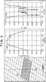
- FIG. 1 is an overall schematic diagram showing a dual band low-dimensioned antenna 101 according to the first example which does not form part of the claimed invention.
- the dual band low-dimensioned antenna 101 includes a substrate on which EBG structure unit cells 102 are arranged in an 8 ⁇ 8 matrix, and a dual frequency orthogonal dipole antenna 103 is arranged parallel to the substrate in the central region thereof.
- the unit cells 102 each have a mushroom structure with a rectangular shape of approximately 10 ⁇ 15 mm, and are arranged periodically in a matrix such that the effect of a artificial magnetic conductor is exhibited.
- FIG. 2 is a model diagram in the case of performing simulation analysis on the EBG structure unit cells 102.
- Each unit cell 102 is constituted by an upper rectangular patch conductor 201, a dielectric layer 202, a lower GND conductor 203, and a connection via 204 that connects these conductors of the multilayer structure.
- An electromagnetic wave incidence surface 205 is set for analysis in order to observe the artificial magnetic conductor characteristics of the unit cell 102.
- the phase of reflected waves in the EBG structure is analyzed at the electromagnetic wave incidence surface 205 with respect to electromagnetic waves in the direction of an arrow 206 and electromagnetic waves in the direction of an arrow 207.
- a surface 208 is a surface forming a boundary of the periodic structure, and the analysis space is set as the period structure including repeating unit cell structures at four surfaces in the horizontal direction.
- FIG. 3 is a graph showing the results of analyzing the model shown in FIG. 2 .
- the horizontal axis indicates the frequency
- the vertical axis indicates the reflected wave phase.
- a curve 301 indicates change in the reflected wave phase relative to electromagnetic waves in the direction of the arrow 206 in FIG. 2
- a curve 302 indicates change in the reflected wave phase relative to electromagnetic waves in the direction of the arrow 207 in FIG. 2 .
- a range 303 of approximately 45° to 135° is assumed to be the section corresponding to effective operation as a artificial magnetic conductor.
- the curve 301 and the curve 302 indicate effective operation as a artificial magnetic conductor from 4.1 GHz to 5.7 GHz and from 3.4 GHz to 4.1 GHz respectively. Note that although a similar artificial magnetic conductor effect can be expected in the section in which the reflected wave phase is approximately -45° to -135° as well, this region is higher than the frequency range, and therefore the frequency range in the reflection coefficient range 303 from 45° to 135° is used.
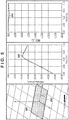
- FIG. 4 shows results confirmed in a simulation of the case where antenna radiation characteristics were ensured by the artificial magnetic conductor effect.
- a substrate 401 is an FR4 substrate in which EBG structure unit cells 102 are arranged in an 8 ⁇ 8 matrix, and a dipole antenna 402 is arranged in the central region thereof.
- the dipole antenna 402 resonates at approximately 5 GHz and is fixed at a height of 1.2 mm from the substrate 401.
- a curve 403 indicates the antenna radiation efficiency
- a curve 404 indicates the antenna S11 reflection characteristic (antenna reflection loss).
- FIG. 5 shows the characteristics of an antenna 502 in the case where conductors not exhibiting the artificial magnetic conductor effect are arranged uniformly.
- the conductors are arranged uniformly on the surface of a substrate 501, and the antenna reflection characteristic is in an approximately total reflection state.
- a curve 503 indicates the antenna radiation efficiency
- a curve 504 indicates the antenna S11 reflection characteristic (antenna reflection loss).
- the curve 503 indicates a 10 dB to 20 dB reduction in radiation efficiency in the vicinity of 5 GHz.
- the curve 504 indicates a 10 dB to 20 dB reduction in the S11 reflection characteristic in the vicinity of 5 GHz.
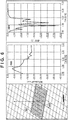
- FIG. 6 shows results confirmed in a simulation of the case where antenna radiation characteristics at a different frequency from FIG. 4 were ensured by the artificial magnetic conductor effect in a different direction.
- a substrate 601 is an FR4 substrate in which EBG structure unit cells 102 are arranged in an 8 ⁇ 8 matrix, and a dipole antenna 602 is arranged in the central region thereof.
- the dipole antenna 602 resonates at approximately 3.7 GHz and is fixed at a height of 1.5 mm from the substrate 601, in a direction orthogonal to the direction of the dipole antenna 402 in FIG. 4 .
- a curve 603 indicates the antenna radiation efficiency
- a curve 604 indicates the antenna S11 reflection characteristic.
- FIG. 7 shows the characteristics of an antenna 702 in the case where conductors not exhibiting the artificial magnetic conductor effect are arranged uniformly instead of a artificial magnetic conductor.
- the conductors are arranged uniformly on the surface of a substrate 701, and the antenna reflection characteristic is in an approximately total reflection state.
- a curve 703 indicates the antenna radiation efficiency
- a curve 704 indicates the antenna S11 reflection characteristic (antenna reflection loss). In comparison with the curve 603 in FIG. 6 , it can be confirmed that the curve
- the curve 703 indicates a 10 dB to 20 dB reduction in radiation efficiency in the vicinity of 3.7 GHz. Also, in comparison with the curve 604 in FIG. 6 , it can be confirmed that the curve 704 indicates a 10 dB to 20 dB reduction in the S11 reflection characteristic in the vicinity of 3.7 GHz.
- a multiband antenna As described above by arranging multiple antenna elements in multiple directions for exhibiting desired artificial magnetic conductor effects on the surface of an EBG structure, it is possible to realize dimension lowering in a multiband antenna. Specifically it is possible to configure a dual band low-dimensioned antenna by arranging a dipole antenna at the short distance of 1.2 to 1.5 mm from an EBG substrate having a GND layer on the underside as shown in FIG. 1 . This distance of 1.2 to 1.5 mm is shorter than 1/4 the wavelength of the resonance frequency band. Also, when designing the arrangement of a built-in antenna in a product, it is possible to realize an antenna arrangement that does not allow radiation characteristic degradation even in the vicinity of a member that causes antenna operation degradation such as a circuit substrate or a metal frame.
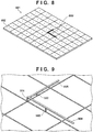
- FIG. 8 is an overall schematic diagram showing a dual band low-dimensioned antenna 801 according to the present embodiment.
- the dual band low-dimensioned antenna 801 according to the present embodiment includes a substrate on which EBG structure unit cells 802 are arranged in an 8 ⁇ 8 matrix, and a dual frequency orthogonal inverted F antenna 803 is arranged parallel to the substrate in the central region thereof.
- the EBG structure made up of the unit cells 802 has a configuration similar to the configuration described in the first embodiment, and exhibits a artificial magnetic conductor effect.
- FIG. 9 shows the configuration of the dual frequency orthogonal inverted F antenna.
- a supply line 901 is a signal line that transmits wireless signals from a circuit portion arranged on the underside of the substrate constituting the EBG structure, for example.
- Elements 902 and 903 are GND elements of two inverted F antenna element conductors 904 and 905, are connected to a GND conductor on the underside of the substrate constituting the EBG structure, and perform impedance matching for the inverted F antennas.
- the antenna element conductor 904 and the antenna element conductor 905 can be arranged at mutually different distances from the substrate.
- the inverted F antenna element conductors 904 and 905 are arranged in the top layer, the patch conductor layer of the EBG structure made up of unit cells 802 is arranged in the second layer, and the GND layer is arranged in the bottom layer.
- the vias constituting the EBG structure, the supply line 901, and the GND elements 902 and 903 of the two inverted F antennas are integrated.
- the circuit substrate layer below the GND layer it is possible to also configure a substrate integrated with a wireless circuit.
- the present embodiment it is possible to realize dimension lowering in a multiband antenna similarly to the first example. Also, when designing the arrangement of a built-in antenna in a product, it is possible to realize an antenna arrangement that does not allow radiation characteristic degradation even in the case of mounting in the vicinity of a member that causes antenna operation degradation such as a metal frame or the substrate for circuitry other than the wireless portion.
- EBG structure having a mushroom structure with rectangular patches is used in the above-described embodiments, there is no limitation to this.
- the directions of the artificial magnetic conductors are set to orthogonal directions in the above-described embodiments, there is no limitation to this. For example, even with directions set to 45° angles or other angles, with any structure in which artificial magnetic conductor effects as components are observed, by aligning the resonance directions of the antenna elements with the directions of the artificial magnetic conductor components, similar effects can be exhibited.
Landscapes
- Physics & Mathematics (AREA)
- Optics & Photonics (AREA)
- Details Of Aerials (AREA)
- Aerials With Secondary Devices (AREA)
- Variable-Direction Aerials And Aerial Arrays (AREA)
Description
- The present invention relates to an antenna device. In particular, the present invention relates to a planar structure having a high surface impedance, and an antenna device employing this planar structure.
- In recent years, research has been conducted on technology related to an electromagnetic band gap structure (hereinafter "EBG structure") that blocks the propagation of electromagnetic waves in a specific frequency bandwidth. One conceivable EBG structure has a structure in which rectangular patch conductors are arranged in a matrix in the same plane with a constant gap interval, and conductive vias from the patch conductors are connected to ground conductors arranged parallel to the patch conductors. In this structure, the set of one patch conductor, one ground conductor, and one conductive via is called a mushroom structure due to its shape. Besides blocking electromagnetic waves, this EBG structure also exhibits an effect of a artificial magnetic conductor that has a high surface impedance in a specific frequency bandwidth. By focusing on this artificial magnetic conductor characteristic and using the EBG structure for antenna dimension lowering, there is expectation for realizing an effective artificial magnetic conductor type low-dimensioned antenna.
- With conventional artificial magnetic conductor type low-dimensioned antennas that employ an EBG structure, it has only been possible to realize a structure in which one EBG structure is provided for one antenna element, and therefore it has been difficult to achieve dimension lowering in a multiband antenna.
- The document
JP 2005 094360 A - The present invention has been achieved in light of the above-described circumstances, and provides a low-dimensioned antenna that can operate at multiple resonance frequencies.
- The present invention in a first aspect provides an antenna device as specified in claims 1 to 6.
- Further features of the present invention will become apparent from the following description of exemplary embodiments with reference to the attached drawings.
-
-
FIG. 1 is a diagram showing a configuration of a dual band low-dimensioned antenna according to a first example not forming part of the claimed invention. -
FIG. 2 is a model diagram in the case of performing simulation analysis on unit cells of an EBG structure. -
FIG. 3 is a diagram showing results of analysis on the dual band low-dimensioned antenna according to the first example. -
FIG. 4 is a diagram showing antenna radiation characteristics according to the first example. -
FIG. 5 is a diagram showing antenna radiation characteristics according to a conventional example. -
FIG. 6 is another diagram showing antenna radiation characteristics according to the first example. -
FIG. 7 is another diagram showing antenna radiation characteristics according to the conventional example. -
FIG. 8 is a schematic diagram of a dual band low-dimensioned antenna according to a first embodiment. -
FIG. 9 is a diagram showing a configuration of a dual frequency orthogonal inverted F antenna. - One feature of a metamaterial structure is the artificial magnetic conductor effect. The surface provided with the periodic structure is a structure having a high surface impedance and realizes in-phase reflection in a specific frequency bandwidth. With a metamaterial artificial magnetic conductor that has a periodic structure made up of repeating unit cell structures, a structure having different artificial magnetic conductor characteristics in two directions can be realized by setting asymmetric conditions for the unit cell structure and periodic structure. For example, in a artificial magnetic conductor having a mushroom structure made up of a patch conductor having different dimensions in the vertical and horizontal directions, artificial magnetic conductor effects corresponding to two different frequency bandwidths are obtained. If antenna elements that operate in two frequency bands are arranged such that their structures have different resonance directions, and a periodic structure having artificial magnetic conductor structures exhibiting effects in the two operating bands of the antennas is arranged below the antenna elements, it is possible to realize a low-dimensioned dual band antenna in which influence from the GND conductor on the underside has been mitigated. Two examples will be described below.
-
FIG. 1 is an overall schematic diagram showing a dual band low-dimensioned antenna 101 according to the first example which does not form part of the claimed invention. The dual band low-dimensioned antenna 101 includes a substrate on which EBGstructure unit cells 102 are arranged in an 8×8 matrix, and a dual frequencyorthogonal dipole antenna 103 is arranged parallel to the substrate in the central region thereof. Theunit cells 102 each have a mushroom structure with a rectangular shape of approximately 10×15 mm, and are arranged periodically in a matrix such that the effect of a artificial magnetic conductor is exhibited. -
FIG. 2 is a model diagram in the case of performing simulation analysis on the EBGstructure unit cells 102. Eachunit cell 102 is constituted by an upperrectangular patch conductor 201, adielectric layer 202, alower GND conductor 203, and a connection via 204 that connects these conductors of the multilayer structure. An electromagneticwave incidence surface 205 is set for analysis in order to observe the artificial magnetic conductor characteristics of theunit cell 102. The phase of reflected waves in the EBG structure is analyzed at the electromagneticwave incidence surface 205 with respect to electromagnetic waves in the direction of anarrow 206 and electromagnetic waves in the direction of anarrow 207. Asurface 208 is a surface forming a boundary of the periodic structure, and the analysis space is set as the period structure including repeating unit cell structures at four surfaces in the horizontal direction. -
FIG. 3 is a graph showing the results of analyzing the model shown inFIG. 2 . InFIG. 3 , the horizontal axis indicates the frequency, and the vertical axis indicates the reflected wave phase. Acurve 301 indicates change in the reflected wave phase relative to electromagnetic waves in the direction of thearrow 206 inFIG. 2 , and acurve 302 indicates change in the reflected wave phase relative to electromagnetic waves in the direction of thearrow 207 inFIG. 2 . Within the range in which the reflected wave phase is not ±180°, arange 303 of approximately 45° to 135° is assumed to be the section corresponding to effective operation as a artificial magnetic conductor. In this case, it can be said that thecurve 301 and thecurve 302 indicate effective operation as a artificial magnetic conductor from 4.1 GHz to 5.7 GHz and from 3.4 GHz to 4.1 GHz respectively. Note that although a similar artificial magnetic conductor effect can be expected in the section in which the reflected wave phase is approximately -45° to -135° as well, this region is higher than the frequency range, and therefore the frequency range in thereflection coefficient range 303 from 45° to 135° is used. -
FIG. 4 shows results confirmed in a simulation of the case where antenna radiation characteristics were ensured by the artificial magnetic conductor effect. Asubstrate 401 is an FR4 substrate in which EBGstructure unit cells 102 are arranged in an 8×8 matrix, and adipole antenna 402 is arranged in the central region thereof. Thedipole antenna 402 resonates at approximately 5 GHz and is fixed at a height of 1.2 mm from thesubstrate 401. Acurve 403 indicates the antenna radiation efficiency, and acurve 404 indicates the antenna S11 reflection characteristic (antenna reflection loss). It can be understood from the features of thecurve 403 that the radiation efficiency is high in the vicinity of 5 GHz, and it can be understood from the features of thecurve 404 that the S11 reflection characteristic is suppressed to a low level in the vicinity of 5 GHz. In other words, it can be understood from these curves that electromagnetic wave radiation is not inhibited by the artificial magnetic conductor effect at the resonance frequency of the dipole antenna. - For comparison,
FIG. 5 shows the characteristics of anantenna 502 in the case where conductors not exhibiting the artificial magnetic conductor effect are arranged uniformly. The conductors are arranged uniformly on the surface of asubstrate 501, and the antenna reflection characteristic is in an approximately total reflection state. Acurve 503 indicates the antenna radiation efficiency, and acurve 504 indicates the antenna S11 reflection characteristic (antenna reflection loss). In comparison with thecurve 403 inFIG. 4 , it can be confirmed that thecurve 503 indicates a 10 dB to 20 dB reduction in radiation efficiency in the vicinity of 5 GHz. Also, in comparison with thecurve 404 inFIG. 4 , it can be confirmed that thecurve 504 indicates a 10 dB to 20 dB reduction in the S11 reflection characteristic in the vicinity of 5 GHz. -
FIG. 6 shows results confirmed in a simulation of the case where antenna radiation characteristics at a different frequency fromFIG. 4 were ensured by the artificial magnetic conductor effect in a different direction. Similarly toFIG. 4 , asubstrate 601 is an FR4 substrate in which EBGstructure unit cells 102 are arranged in an 8×8 matrix, and adipole antenna 602 is arranged in the central region thereof. Thedipole antenna 602 resonates at approximately 3.7 GHz and is fixed at a height of 1.5 mm from thesubstrate 601, in a direction orthogonal to the direction of thedipole antenna 402 inFIG. 4 . Acurve 603 indicates the antenna radiation efficiency, and acurve 604 indicates the antenna S11 reflection characteristic. It can be understood from the features of thecurve 603 that the radiation efficiency is high in the vicinity of 3.7 GHz, and it can be understood from the features of thecurve 604 that the S11 reflection characteristic is suppressed to a low level in the vicinity of 3.7 GHz. In other words, it can be understood from these curves that electromagnetic wave radiation is not inhibited by the artificial magnetic conductor effect at the resonance frequency of thedipole antenna 602. - For comparison,
FIG. 7 shows the characteristics of anantenna 702 in the case where conductors not exhibiting the artificial magnetic conductor effect are arranged uniformly instead of a artificial magnetic conductor. The conductors are arranged uniformly on the surface of asubstrate 701, and the antenna reflection characteristic is in an approximately total reflection state. Acurve 703 indicates the antenna radiation efficiency, and acurve 704 indicates the antenna S11 reflection characteristic (antenna reflection loss). In comparison with thecurve 603 inFIG. 6 , it can be confirmed that the curve - 703 indicates a 10 dB to 20 dB reduction in radiation efficiency in the vicinity of 3.7 GHz. Also, in comparison with the
curve 604 inFIG. 6 , it can be confirmed that thecurve 704 indicates a 10 dB to 20 dB reduction in the S11 reflection characteristic in the vicinity of 3.7 GHz. - As described above by arranging multiple antenna elements in multiple directions for exhibiting desired artificial magnetic conductor effects on the surface of an EBG structure, it is possible to realize dimension lowering in a multiband antenna. Specifically it is possible to configure a dual band low-dimensioned antenna by arranging a dipole antenna at the short distance of 1.2 to 1.5 mm from an EBG substrate having a GND layer on the underside as shown in
FIG. 1 . This distance of 1.2 to 1.5 mm is shorter than 1/4 the wavelength of the resonance frequency band. Also, when designing the arrangement of a built-in antenna in a product, it is possible to realize an antenna arrangement that does not allow radiation characteristic degradation even in the vicinity of a member that causes antenna operation degradation such as a circuit substrate or a metal frame. -
FIG. 8 is an overall schematic diagram showing a dual band low-dimensionedantenna 801 according to the present embodiment. The dual band low-dimensionedantenna 801 according to the present embodiment includes a substrate on which EBGstructure unit cells 802 are arranged in an 8×8 matrix, and a dual frequency orthogonalinverted F antenna 803 is arranged parallel to the substrate in the central region thereof. The EBG structure made up of theunit cells 802 has a configuration similar to the configuration described in the first embodiment, and exhibits a artificial magnetic conductor effect. -
FIG. 9 shows the configuration of the dual frequency orthogonal inverted F antenna. Asupply line 901 is a signal line that transmits wireless signals from a circuit portion arranged on the underside of the substrate constituting the EBG structure, for example.Elements antenna element conductors antenna element conductor 904 and theantenna element conductor 905 can be arranged at mutually different distances from the substrate. - In the present embodiment, the inverted F
antenna element conductors unit cells 802 is arranged in the second layer, and the GND layer is arranged in the bottom layer. Using vias connecting the layers, it is possible to configure a multilayer substrate in which the vias constituting the EBG structure, thesupply line 901, and theGND elements antenna 801 of the present embodiment on one FR4 substrate. Furthermore, by arranging the circuit substrate layer below the GND layer, it is possible to also configure a substrate integrated with a wireless circuit. - As described above, according to the present embodiment, it is possible to realize dimension lowering in a multiband antenna similarly to the first example. Also, when designing the arrangement of a built-in antenna in a product, it is possible to realize an antenna arrangement that does not allow radiation characteristic degradation even in the case of mounting in the vicinity of a member that causes antenna operation degradation such as a metal frame or the substrate for circuitry other than the wireless portion.
- Although an EBG structure having a mushroom structure with rectangular patches is used in the above-described embodiments, there is no limitation to this. There are other techniques for realizing a structure that exhibits artificial magnetic conductor characteristics in multiple directions, and effects similar to the above embodiments can be exhibited with these other techniques as well. Also, although the directions of the artificial magnetic conductors are set to orthogonal directions in the above-described embodiments, there is no limitation to this. For example, even with directions set to 45° angles or other angles, with any structure in which artificial magnetic conductor effects as components are observed, by aligning the resonance directions of the antenna elements with the directions of the artificial magnetic conductor components, similar effects can be exhibited.
- While the present invention has been described with reference to exemplary embodiments, it is to be understood that the invention is not limited to the disclosed exemplary embodiments. The scope of the following claims is to be accorded the broadest interpretation so as to encompass all such modifications and functions.
Claims (6)
- An antenna device (801) comprising a cell structure including a plurality of cells (802) arranged in a matrix, each cell comprising a rectangular patch conductor (201), a GND conductor (203), and a connection via (204) that connects the patch conductor and the GND conductor, and further comprising a first antenna element and a second antenna element (803) arranged over the cell structure, characterized in that the first and second antenna elements are inverted F antenna element conductors (904,905), and the first antenna element and the second antenna element are connected to a supply line (901) which is arranged in parallel with the connection via, and are connected to the GND conductor by GND elements (902, 903) which are arranged in parallel with the connection via, respectively, and
the first antenna element is arranged parallel with a long side of the patch conductor, and the second antenna element is arranged parallel with a short side of the patch conductor. - The antenna device according to claim 1, wherein the first antenna element exhibits resonance in a direction parallel with a long side of the patch conductor, and the second antenna element exhibits resonance in a direction parallel with a short side of the patch conductor.
- The antenna device according to any one of claims 1 or 2,
wherein the first antenna element is arranged such that a distance from the cell structure is shorter than 1/4 a wavelength of a frequency at which the first antenna element exhibits resonance, and
the second antenna element is arranged such that a distance from the cell structure is shorter than 1/4 a wavelength of a frequency at which the second antenna element exhibits resonance. - The antenna device according to any one of claims 1 to 3, wherein the first antenna element and the second antenna element are arranged at mutually different distances from the cell structure.
- The antenna device according to any one of claims 1 to 4, wherein the first antenna element and the second antenna element are arranged so as to exhibit resonance in orthogonal directions.
- The antenna device according to any one of claims 1 to 5, wherein the cell structure is an electromagnetic band gap, EBG, structure.
Applications Claiming Priority (1)
| Application Number | Priority Date | Filing Date | Title |
|---|---|---|---|
| JP2014059076A JP2015185946A (en) | 2014-03-20 | 2014-03-20 | antenna device |
Publications (2)
| Publication Number | Publication Date |
|---|---|
| EP2922143A1 EP2922143A1 (en) | 2015-09-23 |
| EP2922143B1 true EP2922143B1 (en) | 2020-02-12 |
Family
ID=52684165
Family Applications (1)
| Application Number | Title | Priority Date | Filing Date |
|---|---|---|---|
| EP15159932.1A Active EP2922143B1 (en) | 2014-03-20 | 2015-03-19 | Antenna device |
Country Status (4)
| Country | Link |
|---|---|
| US (1) | US9825369B2 (en) |
| EP (1) | EP2922143B1 (en) |
| JP (1) | JP2015185946A (en) |
| KR (1) | KR20150110373A (en) |
Families Citing this family (67)
| Publication number | Priority date | Publication date | Assignee | Title |
|---|---|---|---|---|
| US12057715B2 (en) | 2012-07-06 | 2024-08-06 | Energous Corporation | Systems and methods of wirelessly delivering power to a wireless-power receiver device in response to a change of orientation of the wireless-power receiver device |
| US10256657B2 (en) | 2015-12-24 | 2019-04-09 | Energous Corporation | Antenna having coaxial structure for near field wireless power charging |
| US9876394B1 (en) | 2014-05-07 | 2018-01-23 | Energous Corporation | Boost-charger-boost system for enhanced power delivery |
| US10312715B2 (en) | 2015-09-16 | 2019-06-04 | Energous Corporation | Systems and methods for wireless power charging |
| US10992187B2 (en) | 2012-07-06 | 2021-04-27 | Energous Corporation | System and methods of using electromagnetic waves to wirelessly deliver power to electronic devices |
| US10965164B2 (en) | 2012-07-06 | 2021-03-30 | Energous Corporation | Systems and methods of wirelessly delivering power to a receiver device |
| US9787103B1 (en) | 2013-08-06 | 2017-10-10 | Energous Corporation | Systems and methods for wirelessly delivering power to electronic devices that are unable to communicate with a transmitter |
| US9867062B1 (en) | 2014-07-21 | 2018-01-09 | Energous Corporation | System and methods for using a remote server to authorize a receiving device that has requested wireless power and to determine whether another receiving device should request wireless power in a wireless power transmission system |
| US10992185B2 (en) | 2012-07-06 | 2021-04-27 | Energous Corporation | Systems and methods of using electromagnetic waves to wirelessly deliver power to game controllers |
| US10063105B2 (en) | 2013-07-11 | 2018-08-28 | Energous Corporation | Proximity transmitters for wireless power charging systems |
| US10439448B2 (en) | 2014-08-21 | 2019-10-08 | Energous Corporation | Systems and methods for automatically testing the communication between wireless power transmitter and wireless power receiver |
| US10381880B2 (en) | 2014-07-21 | 2019-08-13 | Energous Corporation | Integrated antenna structure arrays for wireless power transmission |
| US11502551B2 (en) | 2012-07-06 | 2022-11-15 | Energous Corporation | Wirelessly charging multiple wireless-power receivers using different subsets of an antenna array to focus energy at different locations |
| US10158257B2 (en) | 2014-05-01 | 2018-12-18 | Energous Corporation | System and methods for using sound waves to wirelessly deliver power to electronic devices |
| US10068703B1 (en) | 2014-07-21 | 2018-09-04 | Energous Corporation | Integrated miniature PIFA with artificial magnetic conductor metamaterials |
| US10068181B1 (en) | 2015-04-27 | 2018-09-04 | Rigetti & Co, Inc. | Microwave integrated quantum circuits with cap wafer and methods for making the same |
| US10523033B2 (en) | 2015-09-15 | 2019-12-31 | Energous Corporation | Receiver devices configured to determine location within a transmission field |
| US10778041B2 (en) | 2015-09-16 | 2020-09-15 | Energous Corporation | Systems and methods for generating power waves in a wireless power transmission system |
| US11710321B2 (en) | 2015-09-16 | 2023-07-25 | Energous Corporation | Systems and methods of object detection in wireless power charging systems |
| US10734717B2 (en) | 2015-10-13 | 2020-08-04 | Energous Corporation | 3D ceramic mold antenna |
| KR101698131B1 (en) * | 2015-10-22 | 2017-01-19 | 아주대학교 산학협력단 | Broadband circularly polarized antenna using with metasurface |
| US10027180B1 (en) | 2015-11-02 | 2018-07-17 | Energous Corporation | 3D triple linear antenna that acts as heat sink |
| US10063108B1 (en) | 2015-11-02 | 2018-08-28 | Energous Corporation | Stamped three-dimensional antenna |
| US11863001B2 (en) | 2015-12-24 | 2024-01-02 | Energous Corporation | Near-field antenna for wireless power transmission with antenna elements that follow meandering patterns |
| US10038332B1 (en) | 2015-12-24 | 2018-07-31 | Energous Corporation | Systems and methods of wireless power charging through multiple receiving devices |
| US10027159B2 (en) * | 2015-12-24 | 2018-07-17 | Energous Corporation | Antenna for transmitting wireless power signals |
| US10079515B2 (en) | 2016-12-12 | 2018-09-18 | Energous Corporation | Near-field RF charging pad with multi-band antenna element with adaptive loading to efficiently charge an electronic device at any position on the pad |
| US20170270624A1 (en) * | 2016-03-15 | 2017-09-21 | Waterfind USA, Inc. | Systems and Methods for Imputing Groundwater Usage in a Groundwater Basin |
| FR3052617B1 (en) * | 2016-06-14 | 2019-04-05 | Parrot Drones | COMPACT WIFI ANTENNA WITH METAMATERIAL REFLECTOR |
| JP6742666B2 (en) * | 2016-08-17 | 2020-08-19 | 日本アンテナ株式会社 | Planar antenna |
| JP6710437B2 (en) * | 2016-10-09 | 2020-06-17 | 華為技術有限公司Huawei Technologies Co.,Ltd. | Frequency selective surface |
| US10923954B2 (en) | 2016-11-03 | 2021-02-16 | Energous Corporation | Wireless power receiver with a synchronous rectifier |
| CN110535252A (en) | 2016-12-12 | 2019-12-03 | 艾诺格思公司 | For managing the integrated circuit and radio frequency emitting devices of the operation of transmitting equipment |
| US10680319B2 (en) | 2017-01-06 | 2020-06-09 | Energous Corporation | Devices and methods for reducing mutual coupling effects in wireless power transmission systems |
| US10439442B2 (en) | 2017-01-24 | 2019-10-08 | Energous Corporation | Microstrip antennas for wireless power transmitters |
| CN106911001B (en) * | 2017-02-09 | 2019-10-22 | 南京邮电大学 | A kind of dynamic multi-frequency multi-beam space arbitrary scan reflective array |
| US10862198B2 (en) | 2017-03-14 | 2020-12-08 | R.A. Miller Industries, Inc. | Wideband, low profile, small area, circular polarized uhf antenna |
| US11011942B2 (en) | 2017-03-30 | 2021-05-18 | Energous Corporation | Flat antennas having two or more resonant frequencies for use in wireless power transmission systems |
| US10594387B2 (en) | 2017-04-18 | 2020-03-17 | Ajou University Industry-Academic Cooperation Foundation | Solar cell integrated with radio wave transceiving apparatus |
| US10511097B2 (en) | 2017-05-12 | 2019-12-17 | Energous Corporation | Near-field antennas for accumulating energy at a near-field distance with minimal far-field gain |
| US12074452B2 (en) | 2017-05-16 | 2024-08-27 | Wireless Electrical Grid Lan, Wigl Inc. | Networked wireless charging system |
| US11462949B2 (en) | 2017-05-16 | 2022-10-04 | Wireless electrical Grid LAN, WiGL Inc | Wireless charging method and system |
| US12074460B2 (en) | 2017-05-16 | 2024-08-27 | Wireless Electrical Grid Lan, Wigl Inc. | Rechargeable wireless power bank and method of using |
| GB201708242D0 (en) * | 2017-05-23 | 2017-07-05 | Univ Bradford | Radiation shield |
| US11276727B1 (en) | 2017-06-19 | 2022-03-15 | Rigetti & Co, Llc | Superconducting vias for routing electrical signals through substrates and their methods of manufacture |
| US11121301B1 (en) | 2017-06-19 | 2021-09-14 | Rigetti & Co, Inc. | Microwave integrated quantum circuits with cap wafers and their methods of manufacture |
| US10848853B2 (en) | 2017-06-23 | 2020-11-24 | Energous Corporation | Systems, methods, and devices for utilizing a wire of a sound-producing device as an antenna for receipt of wirelessly delivered power |
| KR101895723B1 (en) * | 2017-07-11 | 2018-09-05 | 홍익대학교 산학협력단 | Directional monopole array antenna using hybrid type ground plane |
| US11342798B2 (en) | 2017-10-30 | 2022-05-24 | Energous Corporation | Systems and methods for managing coexistence of wireless-power signals and data signals operating in a same frequency band |
| CN109841941B (en) * | 2017-11-29 | 2021-06-04 | 华为技术有限公司 | Dual-band antenna and wireless communication device |
| US10615647B2 (en) | 2018-02-02 | 2020-04-07 | Energous Corporation | Systems and methods for detecting wireless power receivers and other objects at a near-field charging pad |
| US11159057B2 (en) | 2018-03-14 | 2021-10-26 | Energous Corporation | Loop antennas with selectively-activated feeds to control propagation patterns of wireless power signals |
| US11515732B2 (en) | 2018-06-25 | 2022-11-29 | Energous Corporation | Power wave transmission techniques to focus wirelessly delivered power at a receiving device |
| US11437735B2 (en) | 2018-11-14 | 2022-09-06 | Energous Corporation | Systems for receiving electromagnetic energy using antennas that are minimally affected by the presence of the human body |
| JP2022523022A (en) | 2019-01-28 | 2022-04-21 | エナージャス コーポレイション | Systems and methods for small antennas for wireless power transfer |
| KR20210123329A (en) | 2019-02-06 | 2021-10-13 | 에너저스 코포레이션 | System and method for estimating optimal phase for use with individual antennas in an antenna array |
| CN114731061A (en) | 2019-09-20 | 2022-07-08 | 艾诺格思公司 | Classifying and detecting foreign objects using a power amplifier controller integrated circuit in a wireless power transmission system |
| CN115104234A (en) | 2019-09-20 | 2022-09-23 | 艾诺格思公司 | System and method for protecting a wireless power receiver using multiple rectifiers and establishing in-band communication using multiple rectifiers |
| WO2021055898A1 (en) | 2019-09-20 | 2021-03-25 | Energous Corporation | Systems and methods for machine learning based foreign object detection for wireless power transmission |
| US11381118B2 (en) | 2019-09-20 | 2022-07-05 | Energous Corporation | Systems and methods for machine learning based foreign object detection for wireless power transmission |
| US11355966B2 (en) | 2019-12-13 | 2022-06-07 | Energous Corporation | Charging pad with guiding contours to align an electronic device on the charging pad and efficiently transfer near-field radio-frequency energy to the electronic device |
| US10985617B1 (en) | 2019-12-31 | 2021-04-20 | Energous Corporation | System for wirelessly transmitting energy at a near-field distance without using beam-forming control |
| US11799324B2 (en) | 2020-04-13 | 2023-10-24 | Energous Corporation | Wireless-power transmitting device for creating a uniform near-field charging area |
| JP7182137B2 (en) * | 2020-07-31 | 2022-12-02 | パナソニックIpマネジメント株式会社 | Antenna device and communication device |
| US11735819B2 (en) * | 2020-10-20 | 2023-08-22 | Qualcomm Incorporated | Compact patch and dipole interleaved array antenna |
| CN113036442B (en) * | 2021-03-04 | 2024-05-14 | 齐齐哈尔大学 | Multifunctional digital super-surface for four-channel wave front regulation and control |
| US11916398B2 (en) | 2021-12-29 | 2024-02-27 | Energous Corporation | Small form-factor devices with integrated and modular harvesting receivers, and shelving-mounted wireless-power transmitters for use therewith |
Family Cites Families (21)
| Publication number | Priority date | Publication date | Assignee | Title |
|---|---|---|---|---|
| JP3297580B2 (en) | 1996-02-26 | 2002-07-02 | キヤノン株式会社 | Spread spectrum communication equipment |
| US6707841B1 (en) | 1999-05-27 | 2004-03-16 | Canon Kabushiki Kaisha | Spreading code generator |
| US6483481B1 (en) | 2000-11-14 | 2002-11-19 | Hrl Laboratories, Llc | Textured surface having high electromagnetic impedance in multiple frequency bands |
| US6545647B1 (en) * | 2001-07-13 | 2003-04-08 | Hrl Laboratories, Llc | Antenna system for communicating simultaneously with a satellite and a terrestrial system |
| US6657592B2 (en) * | 2002-04-26 | 2003-12-02 | Rf Micro Devices, Inc. | Patch antenna |
| JP2003338783A (en) * | 2002-05-21 | 2003-11-28 | Matsushita Electric Ind Co Ltd | Antenna assembly |
| JP2005094360A (en) * | 2003-09-17 | 2005-04-07 | Kyocera Corp | Antenna device and radio communication apparatus |
| US7145518B2 (en) | 2003-09-30 | 2006-12-05 | Denso Corporation | Multiple-frequency common antenna |
| US7079079B2 (en) * | 2004-06-30 | 2006-07-18 | Skycross, Inc. | Low profile compact multi-band meanderline loaded antenna |
| WO2008050441A1 (en) | 2006-10-26 | 2008-05-02 | Panasonic Corporation | Antenna device |
| KR100859718B1 (en) | 2006-12-04 | 2008-09-23 | 한국전자통신연구원 | Dipole tag antenna mountable on metallic objects using artificial magnetic conductorAMC for wireless identification and wireless identification system using the same dipole tag antenna |
| JP5023853B2 (en) | 2007-07-13 | 2012-09-12 | パナソニック株式会社 | Speaker diaphragm, speaker using the same, and electronic device and apparatus using the speaker |
| US8406452B2 (en) | 2007-07-13 | 2013-03-26 | Panasonic Corporation | Diaphragm for speaker, speaker using the diaphragm, and system using the speaker |
| JP5307610B2 (en) | 2009-04-17 | 2013-10-02 | キヤノン株式会社 | Wireless communication system and communication method |
| JP2011055036A (en) * | 2009-08-31 | 2011-03-17 | Kumamoto Univ | Planar antenna and polarization system of planar antenna |
| JP5723218B2 (en) | 2010-07-13 | 2015-05-27 | キヤノン株式会社 | Loop antenna |
| US9431709B2 (en) * | 2012-04-03 | 2016-08-30 | Wemtec, Inc. | Artificial magnetic conductor antennas with shielded feedlines |
| JP2013243428A (en) | 2012-05-17 | 2013-12-05 | Canon Inc | Structure |
| JP5969821B2 (en) | 2012-05-25 | 2016-08-17 | キヤノン株式会社 | Antenna device |
| JP6204747B2 (en) | 2013-08-21 | 2017-09-27 | キヤノン株式会社 | Electromagnetic band gap device and electronic circuit |
| JP2015043526A (en) * | 2013-08-26 | 2015-03-05 | 株式会社国際電気通信基礎技術研究所 | Antenna apparatus and electromagnetic wave energy recovery apparatus |
-
2014
- 2014-03-20 JP JP2014059076A patent/JP2015185946A/en active Pending
-
2015
- 2015-03-11 US US14/644,459 patent/US9825369B2/en active Active
- 2015-03-19 KR KR1020150038126A patent/KR20150110373A/en not_active Application Discontinuation
- 2015-03-19 EP EP15159932.1A patent/EP2922143B1/en active Active
Non-Patent Citations (1)
| Title |
|---|
| None * |
Also Published As
| Publication number | Publication date |
|---|---|
| KR20150110373A (en) | 2015-10-02 |
| US9825369B2 (en) | 2017-11-21 |
| EP2922143A1 (en) | 2015-09-23 |
| JP2015185946A (en) | 2015-10-22 |
| US20150270622A1 (en) | 2015-09-24 |
Similar Documents
| Publication | Publication Date | Title |
|---|---|---|
| EP2922143B1 (en) | Antenna device | |
| US11362441B2 (en) | Ultra compact ultra broad band dual polarized base station antenna | |
| US10490346B2 (en) | Antenna structures having planar inverted F-antenna that surrounds an artificial magnetic conductor cell | |
| US9871301B2 (en) | Integrated miniature PIFA with artificial magnetic conductor metamaterials | |
| EP3320580B1 (en) | Metamaterial-based transmitarray for multi-beam antenna array assemblies | |
| CN105322291B (en) | Micro-strip array antenna | |
| JP2018164149A (en) | Antenna device | |
| US10923811B2 (en) | Integrated filtering for band rejection in an antenna element | |
| WO2008128582A1 (en) | Electrical connection elements provided in the amc structure of an antenna arrangement | |
| JP5542902B2 (en) | antenna | |
| CN108429009B (en) | Dual-polarized array antenna structure | |
| JP2014003436A (en) | Antenna device using ebg structure | |
| US20180145417A1 (en) | Reconfigurable compact antenna device | |
| KR20130070332A (en) | Resonance antenna and base-station antenna system having resonance array antenna | |
| JP2012049654A (en) | Ebg structure by divided substrate | |
| US20110240744A1 (en) | Antenna substrate and rfid tag | |
| CN107425269B (en) | Multi-frequency common-caliber broadband radiator | |
| US20190379127A1 (en) | Terminal Antenna and Terminal | |
| Gupta et al. | A broadband dipole on a double layered via-less high impedance surface | |
| Ghaloua et al. | Miniaturization and reduction of mutual coupling for four arrays antennas using new structure of EBG | |
| Karkare et al. | Design of a Rectangular Microstrip Antenna with Artificial Magnetic Conductor Ground Plane | |
| Rajesh et al. | A study of CSRR loaded microstrip antenna for multiband applications | |
| US20170054202A1 (en) | Antenna | |
| Li et al. | A low-profile wideband phased array antenna using ebg structures in p-band | |
| Choi et al. | Isolation enhancement between microstrip patch antennas using dual-band EBG structure without common ground plane |
Legal Events
| Date | Code | Title | Description |
|---|---|---|---|
| PUAI | Public reference made under article 153(3) epc to a published international application that has entered the european phase |
Free format text: ORIGINAL CODE: 0009012 |
|
| AK | Designated contracting states |
Kind code of ref document: A1 Designated state(s): AL AT BE BG CH CY CZ DE DK EE ES FI FR GB GR HR HU IE IS IT LI LT LU LV MC MK MT NL NO PL PT RO RS SE SI SK SM TR |
|
| AX | Request for extension of the european patent |
Extension state: BA ME |
|
| 17P | Request for examination filed |
Effective date: 20160323 |
|
| RBV | Designated contracting states (corrected) |
Designated state(s): AL AT BE BG CH CY CZ DE DK EE ES FI FR GB GR HR HU IE IS IT LI LT LU LV MC MK MT NL NO PL PT RO RS SE SI SK SM TR |
|
| GRAP | Despatch of communication of intention to grant a patent |
Free format text: ORIGINAL CODE: EPIDOSNIGR1 |
|
| STAA | Information on the status of an ep patent application or granted ep patent |
Free format text: STATUS: GRANT OF PATENT IS INTENDED |
|
| RIC1 | Information provided on ipc code assigned before grant |
Ipc: H01Q 21/30 20060101ALI20190729BHEP Ipc: H01Q 15/00 20060101AFI20190729BHEP Ipc: H01Q 9/16 20060101ALI20190729BHEP Ipc: H01Q 5/385 20150101ALI20190729BHEP Ipc: H01Q 21/24 20060101ALI20190729BHEP Ipc: H01Q 1/36 20060101ALI20190729BHEP |
|
| INTG | Intention to grant announced |
Effective date: 20190828 |
|
| GRAS | Grant fee paid |
Free format text: ORIGINAL CODE: EPIDOSNIGR3 |
|
| GRAA | (expected) grant |
Free format text: ORIGINAL CODE: 0009210 |
|
| STAA | Information on the status of an ep patent application or granted ep patent |
Free format text: STATUS: THE PATENT HAS BEEN GRANTED |
|
| AK | Designated contracting states |
Kind code of ref document: B1 Designated state(s): AL AT BE BG CH CY CZ DE DK EE ES FI FR GB GR HR HU IE IS IT LI LT LU LV MC MK MT NL NO PL PT RO RS SE SI SK SM TR |
|
| REG | Reference to a national code |
Ref country code: GB Ref legal event code: FG4D |
|
| REG | Reference to a national code |
Ref country code: CH Ref legal event code: EP |
|
| REG | Reference to a national code |
Ref country code: AT Ref legal event code: REF Ref document number: 1233325 Country of ref document: AT Kind code of ref document: T Effective date: 20200215 |
|
| REG | Reference to a national code |
Ref country code: IE Ref legal event code: FG4D |
|
| REG | Reference to a national code |
Ref country code: DE Ref legal event code: R096 Ref document number: 602015046648 Country of ref document: DE |
|
| PG25 | Lapsed in a contracting state [announced via postgrant information from national office to epo] |
Ref country code: NO Free format text: LAPSE BECAUSE OF FAILURE TO SUBMIT A TRANSLATION OF THE DESCRIPTION OR TO PAY THE FEE WITHIN THE PRESCRIBED TIME-LIMIT Effective date: 20200512 Ref country code: RS Free format text: LAPSE BECAUSE OF FAILURE TO SUBMIT A TRANSLATION OF THE DESCRIPTION OR TO PAY THE FEE WITHIN THE PRESCRIBED TIME-LIMIT Effective date: 20200212 Ref country code: FI Free format text: LAPSE BECAUSE OF FAILURE TO SUBMIT A TRANSLATION OF THE DESCRIPTION OR TO PAY THE FEE WITHIN THE PRESCRIBED TIME-LIMIT Effective date: 20200212 |
|
| REG | Reference to a national code |
Ref country code: LT Ref legal event code: MG4D |
|
| REG | Reference to a national code |
Ref country code: NL Ref legal event code: MP Effective date: 20200212 |
|
| PG25 | Lapsed in a contracting state [announced via postgrant information from national office to epo] |
Ref country code: GR Free format text: LAPSE BECAUSE OF FAILURE TO SUBMIT A TRANSLATION OF THE DESCRIPTION OR TO PAY THE FEE WITHIN THE PRESCRIBED TIME-LIMIT Effective date: 20200513 Ref country code: IS Free format text: LAPSE BECAUSE OF FAILURE TO SUBMIT A TRANSLATION OF THE DESCRIPTION OR TO PAY THE FEE WITHIN THE PRESCRIBED TIME-LIMIT Effective date: 20200612 Ref country code: HR Free format text: LAPSE BECAUSE OF FAILURE TO SUBMIT A TRANSLATION OF THE DESCRIPTION OR TO PAY THE FEE WITHIN THE PRESCRIBED TIME-LIMIT Effective date: 20200212 Ref country code: SE Free format text: LAPSE BECAUSE OF FAILURE TO SUBMIT A TRANSLATION OF THE DESCRIPTION OR TO PAY THE FEE WITHIN THE PRESCRIBED TIME-LIMIT Effective date: 20200212 Ref country code: LV Free format text: LAPSE BECAUSE OF FAILURE TO SUBMIT A TRANSLATION OF THE DESCRIPTION OR TO PAY THE FEE WITHIN THE PRESCRIBED TIME-LIMIT Effective date: 20200212 Ref country code: BG Free format text: LAPSE BECAUSE OF FAILURE TO SUBMIT A TRANSLATION OF THE DESCRIPTION OR TO PAY THE FEE WITHIN THE PRESCRIBED TIME-LIMIT Effective date: 20200512 |
|
| PG25 | Lapsed in a contracting state [announced via postgrant information from national office to epo] |
Ref country code: NL Free format text: LAPSE BECAUSE OF FAILURE TO SUBMIT A TRANSLATION OF THE DESCRIPTION OR TO PAY THE FEE WITHIN THE PRESCRIBED TIME-LIMIT Effective date: 20200212 |
|
| REG | Reference to a national code |
Ref country code: DE Ref legal event code: R119 Ref document number: 602015046648 Country of ref document: DE |
|
| PG25 | Lapsed in a contracting state [announced via postgrant information from national office to epo] |
Ref country code: ES Free format text: LAPSE BECAUSE OF FAILURE TO SUBMIT A TRANSLATION OF THE DESCRIPTION OR TO PAY THE FEE WITHIN THE PRESCRIBED TIME-LIMIT Effective date: 20200212 Ref country code: LT Free format text: LAPSE BECAUSE OF FAILURE TO SUBMIT A TRANSLATION OF THE DESCRIPTION OR TO PAY THE FEE WITHIN THE PRESCRIBED TIME-LIMIT Effective date: 20200212 Ref country code: PT Free format text: LAPSE BECAUSE OF FAILURE TO SUBMIT A TRANSLATION OF THE DESCRIPTION OR TO PAY THE FEE WITHIN THE PRESCRIBED TIME-LIMIT Effective date: 20200705 Ref country code: RO Free format text: LAPSE BECAUSE OF FAILURE TO SUBMIT A TRANSLATION OF THE DESCRIPTION OR TO PAY THE FEE WITHIN THE PRESCRIBED TIME-LIMIT Effective date: 20200212 Ref country code: CZ Free format text: LAPSE BECAUSE OF FAILURE TO SUBMIT A TRANSLATION OF THE DESCRIPTION OR TO PAY THE FEE WITHIN THE PRESCRIBED TIME-LIMIT Effective date: 20200212 Ref country code: EE Free format text: LAPSE BECAUSE OF FAILURE TO SUBMIT A TRANSLATION OF THE DESCRIPTION OR TO PAY THE FEE WITHIN THE PRESCRIBED TIME-LIMIT Effective date: 20200212 Ref country code: SK Free format text: LAPSE BECAUSE OF FAILURE TO SUBMIT A TRANSLATION OF THE DESCRIPTION OR TO PAY THE FEE WITHIN THE PRESCRIBED TIME-LIMIT Effective date: 20200212 Ref country code: SM Free format text: LAPSE BECAUSE OF FAILURE TO SUBMIT A TRANSLATION OF THE DESCRIPTION OR TO PAY THE FEE WITHIN THE PRESCRIBED TIME-LIMIT Effective date: 20200212 Ref country code: DK Free format text: LAPSE BECAUSE OF FAILURE TO SUBMIT A TRANSLATION OF THE DESCRIPTION OR TO PAY THE FEE WITHIN THE PRESCRIBED TIME-LIMIT Effective date: 20200212 |
|
| REG | Reference to a national code |
Ref country code: CH Ref legal event code: PL |
|
| REG | Reference to a national code |
Ref country code: AT Ref legal event code: MK05 Ref document number: 1233325 Country of ref document: AT Kind code of ref document: T Effective date: 20200212 |
|
| PG25 | Lapsed in a contracting state [announced via postgrant information from national office to epo] |
Ref country code: MC Free format text: LAPSE BECAUSE OF FAILURE TO SUBMIT A TRANSLATION OF THE DESCRIPTION OR TO PAY THE FEE WITHIN THE PRESCRIBED TIME-LIMIT Effective date: 20200212 |
|
| PLBE | No opposition filed within time limit |
Free format text: ORIGINAL CODE: 0009261 |
|
| STAA | Information on the status of an ep patent application or granted ep patent |
Free format text: STATUS: NO OPPOSITION FILED WITHIN TIME LIMIT |
|
| REG | Reference to a national code |
Ref country code: BE Ref legal event code: MM Effective date: 20200331 |
|
| PG25 | Lapsed in a contracting state [announced via postgrant information from national office to epo] |
Ref country code: LU Free format text: LAPSE BECAUSE OF NON-PAYMENT OF DUE FEES Effective date: 20200319 |
|
| 26N | No opposition filed |
Effective date: 20201113 |
|
| PG25 | Lapsed in a contracting state [announced via postgrant information from national office to epo] |
Ref country code: LI Free format text: LAPSE BECAUSE OF NON-PAYMENT OF DUE FEES Effective date: 20200331 Ref country code: FR Free format text: LAPSE BECAUSE OF NON-PAYMENT OF DUE FEES Effective date: 20200412 Ref country code: DE Free format text: LAPSE BECAUSE OF NON-PAYMENT OF DUE FEES Effective date: 20201001 Ref country code: CH Free format text: LAPSE BECAUSE OF NON-PAYMENT OF DUE FEES Effective date: 20200331 Ref country code: IT Free format text: LAPSE BECAUSE OF FAILURE TO SUBMIT A TRANSLATION OF THE DESCRIPTION OR TO PAY THE FEE WITHIN THE PRESCRIBED TIME-LIMIT Effective date: 20200212 Ref country code: AT Free format text: LAPSE BECAUSE OF FAILURE TO SUBMIT A TRANSLATION OF THE DESCRIPTION OR TO PAY THE FEE WITHIN THE PRESCRIBED TIME-LIMIT Effective date: 20200212 Ref country code: IE Free format text: LAPSE BECAUSE OF NON-PAYMENT OF DUE FEES Effective date: 20200319 |
|
| PG25 | Lapsed in a contracting state [announced via postgrant information from national office to epo] |
Ref country code: SI Free format text: LAPSE BECAUSE OF FAILURE TO SUBMIT A TRANSLATION OF THE DESCRIPTION OR TO PAY THE FEE WITHIN THE PRESCRIBED TIME-LIMIT Effective date: 20200212 Ref country code: BE Free format text: LAPSE BECAUSE OF NON-PAYMENT OF DUE FEES Effective date: 20200331 Ref country code: PL Free format text: LAPSE BECAUSE OF FAILURE TO SUBMIT A TRANSLATION OF THE DESCRIPTION OR TO PAY THE FEE WITHIN THE PRESCRIBED TIME-LIMIT Effective date: 20200212 |
|
| PG25 | Lapsed in a contracting state [announced via postgrant information from national office to epo] |
Ref country code: TR Free format text: LAPSE BECAUSE OF FAILURE TO SUBMIT A TRANSLATION OF THE DESCRIPTION OR TO PAY THE FEE WITHIN THE PRESCRIBED TIME-LIMIT Effective date: 20200212 Ref country code: MT Free format text: LAPSE BECAUSE OF FAILURE TO SUBMIT A TRANSLATION OF THE DESCRIPTION OR TO PAY THE FEE WITHIN THE PRESCRIBED TIME-LIMIT Effective date: 20200212 Ref country code: CY Free format text: LAPSE BECAUSE OF FAILURE TO SUBMIT A TRANSLATION OF THE DESCRIPTION OR TO PAY THE FEE WITHIN THE PRESCRIBED TIME-LIMIT Effective date: 20200212 |
|
| PG25 | Lapsed in a contracting state [announced via postgrant information from national office to epo] |
Ref country code: MK Free format text: LAPSE BECAUSE OF FAILURE TO SUBMIT A TRANSLATION OF THE DESCRIPTION OR TO PAY THE FEE WITHIN THE PRESCRIBED TIME-LIMIT Effective date: 20200212 Ref country code: AL Free format text: LAPSE BECAUSE OF FAILURE TO SUBMIT A TRANSLATION OF THE DESCRIPTION OR TO PAY THE FEE WITHIN THE PRESCRIBED TIME-LIMIT Effective date: 20200212 |
|
| PGFP | Annual fee paid to national office [announced via postgrant information from national office to epo] |
Ref country code: GB Payment date: 20240220 Year of fee payment: 10 |