JP5969821B2 - Antenna device - Google Patents
Antenna device Download PDFInfo
- Publication number
- JP5969821B2 JP5969821B2 JP2012120139A JP2012120139A JP5969821B2 JP 5969821 B2 JP5969821 B2 JP 5969821B2 JP 2012120139 A JP2012120139 A JP 2012120139A JP 2012120139 A JP2012120139 A JP 2012120139A JP 5969821 B2 JP5969821 B2 JP 5969821B2
- Authority
- JP
- Japan
- Prior art keywords
- conductor plate
- antenna
- additional conductor
- additional
- frequency
- Prior art date
- Legal status (The legal status is an assumption and is not a legal conclusion. Google has not performed a legal analysis and makes no representation as to the accuracy of the status listed.)
- Active
Links
Images


Classifications
-
- H—ELECTRICITY
- H01—ELECTRIC ELEMENTS
- H01Q—ANTENNAS, i.e. RADIO AERIALS
- H01Q9/00—Electrically-short antennas having dimensions not more than twice the operating wavelength and consisting of conductive active radiating elements
- H01Q9/04—Resonant antennas
- H01Q9/0407—Substantially flat resonant element parallel to ground plane, e.g. patch antenna
-
- H—ELECTRICITY
- H01—ELECTRIC ELEMENTS
- H01Q—ANTENNAS, i.e. RADIO AERIALS
- H01Q1/00—Details of, or arrangements associated with, antennas
- H01Q1/48—Earthing means; Earth screens; Counterpoises
Landscapes
- Waveguide Aerials (AREA)
- Details Of Aerials (AREA)
Description
本発明はアンテナ装置に関する。 The present invention relates to an antenna device.
近年、無線LANやBluetooth(登録商標)等の無線通信機能を備えたパーソナルコンピュータをはじめとする小型の電子機器が普及してきている。無線LANやBluetoothなどの無線通信には、例えば2.4GHz帯や5GHz帯の電波が使用される。無線通信機能を備えたパーソナルコンピュータでは、無線通信用のアンテナを内蔵しており、そのアンテナの形式として、例えばモノポールアンテナ、ヘリカルアンテナ、逆Fアンテナ、パッチアンテナなど、種々のアンテナが採用されている。 In recent years, small electronic devices such as personal computers equipped with a wireless communication function such as a wireless LAN and Bluetooth (registered trademark) have become widespread. For wireless communication such as wireless LAN and Bluetooth, for example, 2.4 GHz band and 5 GHz band radio waves are used. A personal computer equipped with a wireless communication function has a built-in antenna for wireless communication, and various antennas such as a monopole antenna, a helical antenna, an inverted F antenna, and a patch antenna are adopted as the antenna format. Yes.
これらの各種アンテナは、電子機器の小型化やデザイン性の向上を目的として機器内の限られた空間への実装を余儀なくされると共に、コストの低減も要求されている。このデザイン性の向上と低コスト化のため、アンテナは、単独で製品筐体から突出する形で実装されずに、例えば無線モジュールチップと同一の基板上に部品として実装され、外観からはアンテナと判断できない様に製品筐体の内部に配置されることが多い。しかし、小型電子機器においてアンテナを内蔵した場合、アンテナの周囲に十分な空間を確保できないため、アンテナに近接配置された部材によってアンテナの共振状態が変化し、アンテナ単体での周波数特性と実装時の特性が異なってしまうという問題があった。すなわち、アンテナの周辺に金属部品が存在すると、例えば、アンテナからの電磁波でその金属部品に電流が誘起されることや、周辺の金属部品との間で余計な静電容量などが発生することにより、アンテナの共振特性が変化してしまうという問題があった。 These various antennas are required to be mounted in a limited space in the device for the purpose of downsizing the electronic device and improving the design, and cost reduction is also required. In order to improve the design and reduce the cost, the antenna is not mounted in a form that protrudes from the product housing alone, but is mounted as a component on the same substrate as the wireless module chip, for example. It is often placed inside the product housing so that it cannot be determined. However, when an antenna is built in a small electronic device, a sufficient space around the antenna cannot be secured. Therefore, the resonance state of the antenna changes depending on the member arranged close to the antenna. There was a problem that the characteristics were different. That is, if there is a metal part around the antenna, for example, an electric current is induced in the metal part due to electromagnetic waves from the antenna, or extra capacitance is generated between the metal part and the surrounding metal part. There is a problem that the resonance characteristic of the antenna changes.
一般に、無線機器は、使用に際しては電波法に定められた試験を受験し、許認可を受ける必要がある。しかしながら、実装環境による特性変動は製品ごとに異なる事が多いため、機能部品としての無線モジュールを異なるメカ構成の製品に順次搭載する場合は、上述のような理由ではじめに最適化した特定の製品以外では性能が低下する場合があった。 In general, when using a wireless device, it is necessary to take a test prescribed in the Radio Law and obtain permission. However, the characteristic variation due to the mounting environment is often different for each product, so when mounting wireless modules as functional parts sequentially on products with different mechanical configurations, it is not the specific product that was first optimized for the reasons described above. In some cases, performance deteriorated.
パッチアンテナは、このような周辺環境からの影響でもアンテナ特性が比較的変動し難いが、それでも変動しないわけではない。このため、複数製品で共用する場合には、やはり各製品の実装環境に合わせた調整を行うことが要求される。このような、搭載製品ごとの特性調整を複数周波数で行う方法として、特許文献1には、パッチアンテナの給電ピンの構造をねじ式にする事で給電点での容量成分を調整可能とし、機器実装後の特性変動を後から調整可能とする技術が記載されている。
Although the antenna characteristics of the patch antenna are relatively unaffected by the influence of the surrounding environment, it is not necessarily unaffected. For this reason, when sharing with a plurality of products, it is still required to make adjustments according to the mounting environment of each product. As a method of performing characteristic adjustment for each mounted product at a plurality of frequencies,
しかし、特許文献1に記載の技術は、整合回路の容量成分の調整を後から可能とする構成ではあるが、パッチアンテナ素子を構成する給電線路自体の構造を変更してしまう。したがって、このようなアンテナを複数製品へ搭載する場合には、個別調整を盛り込んだ個別のパッチアンテナ素子を用意しなければならないという問題があった。本発明は上記課題に鑑みなされたものであり、異なる製品に対して同一のアンテナ素子及び無線部を使用可能とする技術を提供することを目的とする。
However, although the technology described in
上記目的を達成するため、本発明によるアンテナ装置は、導体板と、前記導体板の一方の面に所定の間隔を空けて対向して設けられる接地導体板と、前記導体板へ給電する給電点とを有し、金属が近接していない条件において第1の共振周波数で動作するパッチアンテナ素子と、前記接地導体板に高周波結合されると共に、前記導体板の中心と前記給電点とを結ぶ直線に直交する方向に延びる形状を有する少なくとも1つの付加導体板と、を有し、金属が近接している第1の実装条件において、前記パッチアンテナ素子と、長さと幅と位置との少なくとも何れかを第1の値にした前記付加導体板とを用いて第1の共振周波数で動作し、前記第1の実装条件とは異なる、金属が近接している第2の実装条件において、前記パッチアンテナ素子と、長さと幅と位置との少なくとも何れかを第2の値にした前記付加導体板とを用いて第1の共振周波数で動作する、ことを特徴とする。
In order to achieve the above object, an antenna device according to the present invention includes a conductor plate, a ground conductor plate provided opposite to one surface of the conductor plate at a predetermined interval, and a feeding point for feeding power to the conductor plate. possess the door, and the patch antenna elements operating at a first resonant frequency in a condition that the metal is not close, along with the high-frequency coupled to the ground conductor plate, connecting the center and the feed point of the conductor plate linear and at least one additional conductor plate has a shape extending in a direction orthogonal, was closed, in a first mounting condition where the metal is close, at least one of the position and the patch antenna elements, the length and width In the second mounting condition that operates at a first resonance frequency using the additional conductor plate having a first value and is different from the first mounting condition, the metal is close to the patch antenna. Element and Operating at a first resonant frequency using at least one of the length and the width and position and the second of the additional conductors and a value plate, characterized in that.
本発明によれば、アンテナ実装部周辺のメカ構成部材によらず、同一のアンテナ素子を用いて目的のアンテナ特性を得ることができるアンテナ装置を提供することができる。 ADVANTAGE OF THE INVENTION According to this invention, the antenna apparatus which can obtain the target antenna characteristic can be provided using the same antenna element irrespective of the mechanical structural member around an antenna mounting part.
以下、添付図面を参照して本発明の実施の形態を詳細に説明する。 Hereinafter, embodiments of the present invention will be described in detail with reference to the accompanying drawings.
<<実施形態1>>
図1は、本実施形態に係るアンテナ装置の構成例を示す図である。図1(A)はアンテナ装置全体を示す図で、パッチアンテナ素子101と付加導体板102及び103とを重ね合わせた構成となっている。
<<
FIG. 1 is a diagram illustrating a configuration example of an antenna device according to the present embodiment. FIG. 1A is a diagram showing the entire antenna device, and has a configuration in which a
図1(B)に、パッチアンテナ素子101の構造の例を詳細に示す。パッチアンテナ素子101は、例えば、2.4GHz帯で動作する円偏波パッチアンテナである。パッチアンテナ素子101は、例えば、給電線104、パッチ導体105、セラミックブロック106、接地導体板107を有する。給電線104はアンテナへの信号入出力ラインであり、共振動作の主体となるパッチ導体105に接続される。セラミックブロック106は、40〜100程度の高い比誘電率を有するセラミックのブロックである。セラミックブロック106により、セラミック素材の比誘電率の平方根に比例して波長短縮効果が得られるため、パッチアンテナ素子全体の小型化が可能となる。接地導体板107はグラウンドとして機能する導体板であり、パッチ導体105の一方の面と対向して、例えばセラミックブロックの厚さである所定の間隔を空けて設置される。接地導体板107は、アンテナとして必要な領域はセラミックブロック106の下面と接する部分になるが、本実施形態では、無線モジュール基板に搭載されるパッチアンテナを想定し、無線機能部品実装領域108を含む例を示している。具体的な個々の部品形状等に関してはここでは説明を省略する。
FIG. 1B shows an example of the structure of the
一般に、パッチアンテナの共振導体(パッチ導体105)は、共振周波数の波長の1/2程度の長さと幅を必要とする。ここで、「長さ」は給電線路と平行になる一辺の事で図の109の部分であり、「幅」は給電線路及び図の109の部分と直交する一辺のことである。長さは主に共振の中心周波数に関連し、幅は主に共振可能な周波数帯域幅に関連する。2.4GHz帯での波長はおよそ120mmであるため、アンテナの素子長としては60mm四方程度の大きさが必要となる。しかしながら、本実施形態では、セラミックブロック106の比誘電率を100程度とし、波長短縮効果を得ることにより、アンテナを1/10程度の寸法で実現するものとする。この小型化により、無線機能部品実装領域108を含むモジュール基板としての寸法を、20mm×10mm程にすることが可能である。
In general, the resonant conductor (patch conductor 105) of the patch antenna requires a length and a width that are about ½ of the wavelength of the resonant frequency. Here, “length” means a side parallel to the feed line and is a
次に、図1(C)に付加導体板の例を示す。付加導体板は、パッチアンテナ素子101の接地導体板107に貼り合わせて使用する構造となっており、張り合わせた際にパッチアンテナ素子101の接地導体板107からはみ出す部分として2つの付加導体板102及び103を有する構造となる。なお、以下の説明では接地導体板107へ2つの付加導体板102及び103が高周波結合されるように説明するが、一方の付加導体板は長さが0mmであってもよい。すなわち、少なくとも1つの付加導体板が付加されればよい。
Next, FIG. 1C shows an example of the additional conductor plate. The additional conductor plate has a structure that is used by being bonded to the
本実施形態においては、付加導体板は、接地導体板107の一辺であって、給電点(給電線104)とパッチ導体105の中心とを結ぶ直線と平行な一辺に接続されるような形状を有するものとして説明する。なお、例えば、接地導体板107の形状が矩形でない場合などでも、付加導体板は、接地導体板107と高周波結合すると共に、給電点とパッチ導体105の中心とを結ぶ直線に直交する方向又は略直交する方向に延びる形状を有するものであればよい。本明細書、特許請求の範囲及び図面では、特別の記載がない限り、略直交も含めて「直交」と記載する。
In the present embodiment, the additional conductor plate has a shape that is connected to one side of the
付加導体板の素材は、例えば導電性の高い部材であり、一般にはコスト要因等を考慮してアルミ板金などを用いてもよいが、これに限定するものではない。図1(C)では、2つの付加導体板102及び103は、高周波結合用領域110を介して接続された一体型の構造となっており、高周波結合用領域110は、パッチアンテナ素子101の接地導体板107と張り合わされる部分となる。なお、このように一体構造とすることにより張り合わせが容易となるが、高周波結合が確保できる構造であれば、付加導体板102及び103を個別に接地導体板107と張り合わせる構造としてもよい。2つの付加導体板102及び103は、それぞれの長さ111及び112を実装条件に合わせて調整することにより、その実装条件下でのアンテナ特性を最適化する。すなわち、周辺に存在する金属部材による共振特性の変化を付加導体板102及び103によって補償し、アンテナ特性を目的の特性に近づける。具体的な調整方法については後述する。
The material of the additional conductor plate is, for example, a highly conductive member, and in general, an aluminum sheet metal or the like may be used in consideration of cost factors, but is not limited thereto. In FIG. 1C, the two
次に、本実施形態におけるアンテナ特性に関して説明する。図1のパッチアンテナ素子101単体での共振特性をシミュレーションにより求めた結果を図2に示す。横軸は周波数を示し、縦軸はアンテナ共振特性をSパラメータS11のリターンロスで示している。S11特性が−10dB以下であれば良好な共振状態を示しており、曲線201は2.51GHzでリターンロス−16dBの最大共振を示し、良好な特性を発揮していることを示している。
Next, antenna characteristics in this embodiment will be described. FIG. 2 shows a result obtained by simulating the resonance characteristics of the
実際にこのアンテナを製品へ搭載する場合、アンテナ周辺に金属部材の近接が無ければ、図2で示されたのと同様の特性が各製品で維持される。しかしながら、周辺のメカ構成によっては、特定の製品への搭載時の特性の劣化や、共振周波数の個別の変動が生じうる。図3に、金属近接による特性変化を起こした例をシミュレーションで検証した結果を示す。図3のシミュレーションにおいては、実装条件として、図3(A)のように、パッチアンテナ素子301の側面から2mm離れた場所に、金属の壁302が配置されている金属近接条件を仮定した。この時の共振特性を図3(B)に示す。図3(B)の曲線303で示すように、この場合の2.4GHz帯の共振特性は、図2で示したアンテナ単体での共振特性に比べてリターンロスが大きく劣化しており、目安となる−10dB以下を達成できない状態になっていることが分かる。また最大共振周波数も2.51GHzから2.53GHzにシフトしてしまっていることも分かる。
When this antenna is actually mounted on a product, the same characteristics as shown in FIG. 2 are maintained in each product if there is no proximity of a metal member around the antenna. However, depending on the surrounding mechanical configuration, characteristic deterioration when mounted on a specific product and individual fluctuations in the resonance frequency may occur. FIG. 3 shows a result of verification by simulation of an example in which a characteristic change due to metal proximity occurs. In the simulation of FIG. 3, a metal proximity condition in which a
ここで、図3(A)の金属近接条件のまま、パッチアンテナ素子に図1(C)で示すような付加導体板を追加する。付加導体板を追加した状態でのアンテナ特性を図4に示す。板金部材の付加により、曲線401で示すように、2.4GHz帯の共振特性はリターンロスが−17dB程度に回復し、最大共振周波数も2.51GHzに戻すことができていることが分かる。なお、この例では、2つの付加導体板の長さは図3(A)の金属近接条件に対して最適化された寸法を用いている。最適な板金の長さについて図5を参照して説明する。
Here, an additional conductor plate as shown in FIG. 1C is added to the patch antenna element while maintaining the metal proximity condition in FIG. FIG. 4 shows the antenna characteristics with the additional conductor plate added. With the addition of the sheet metal member, as shown by the
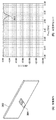
図5(A)に示すように、付加導体板102の長さをL1、付加導体板103の長さをL2とする。L1、L2をそれぞれ0から30mmまで、5mm間隔で変更した際のリターンロスの変化を図5(B)に示す。図5(B)から、2つの付加導体板の長さの組み合わせを変化させることにより、共振周波数のシフトとリターンロスとを変化させることが可能であることが分かる。例えば、曲線501は、L1とL2とをそれぞれ25mmと10mmとした場合のもので、共振周波数は2.48GHzに低下するが、リターンロスは−20dBに達する。曲線502は、L1とL2とをそれぞれ5mmと25mmとした場合のものであり、リターンロスは−23dBに達しており、共振周波数は2.50GHzである。曲線503は、L1とL2とをそれぞれ0mmと25mmとした場合のもので、図4で示した、金属近接のない状態とほぼ同等の特性となる場合のものである。このように、2つの付加導体板の寸法を調整する事で、周波数のずれと共振の劣化とを共に回復させる事が可能となる。そして、例えば、周波数のずれが最も小さく、かつリターンロスが最も小さい板金の長さのパターンを、最適値を与える長さのパターンとする。これ以外にも、目的の最大共振周波数において、リターンロスが最小となる板金の長さのパターンを最適としてもよい。
As shown in FIG. 5A, the length of the
なお、ここまで付加導体板が、パッチアンテナ素子の外周から、接地導体板107を含む面と平行の面上において延びる形状である場合について説明してきたが、これに限定するものではない。例えば図6(A)に示すように、パッチアンテナ側面から真下方向に2つの付加導体板102及び103を延長する配置でも同様の効果を得る事ができる。すなわち、付加導体板が、パッチアンテナ素子101の外周から、接地導体板107を含む面の法線方向であって、パッチ導体105と反対側へ延びる形状をとってもよい。また、必ずしも外周から延びる形状でなくてもよい。すなわち、パッチアンテナの側面よりパッチアンテナの中心側から付加導体板が延びる形状であってもよい。
Although the case where the additional conductor plate has a shape extending from the outer periphery of the patch antenna element on the plane parallel to the plane including the
図6(B)に、近接金属302の条件を図3で示したものと同様とし、最適化の結果としてL1及びL2をそれぞれ15mmと25mmとした場合のアンテナ特性のシミュレーション結果を示す。図6(B)の曲線601に示すように、このように付加導体板を追加することにより、図4の特性とほぼ同等の特性を得ることができていることが分かる。
FIG. 6B shows a simulation result of antenna characteristics when the conditions of the
なお、本実施形態の付加導体板は、少なくとも一部において、パッチ導体105の中心と給電点とを結ぶ直線に直交な方向に延びていればよく、1つの平面上に存在する必要はない。例えば、付加導体板をポリイミド樹脂などで導体箔を覆ったフレキシブル基板構造にする事で局面形状にも対応可能とし、実装部周辺部品の構造に合わせて柔軟に配置するようにしてもよい。
Note that the additional conductor plate of the present embodiment need only extend in a direction orthogonal to a straight line connecting the center of the
以上のように、パッチアンテナ素子のグラウンド領域に高周波接続する構造で、給電線路に直交する方向となる側面に付加導体板を付加し、付加された導体の長さを設定する事で、実装条件に合わせて共振周波数及びリターンロスを調整することができる。これにより、当初設計時にパッチアンテナ素子単体で最適化された状態から、製品実装に際して金属部材の近接等に起因して特性が劣化してしまったパッチアンテナに対して、簡易な部材追加で例えば入力インピーダンスを整合させ、特性を回復させる事ができる。 As described above, a high frequency connection to the ground area of the patch antenna element, an additional conductor plate is added to the side surface that is orthogonal to the feed line, and the length of the added conductor is set. The resonance frequency and return loss can be adjusted according to the above. As a result, from a state where the patch antenna element is optimized at the time of initial design to a patch antenna whose characteristics have deteriorated due to the proximity of a metal member or the like when mounting the product, for example, by simple addition of members Impedance can be matched and characteristics can be restored.
<<実施形態2>>
本実施形態は、実施形態1と同様の実装条件において、共振周波数の調整を広範囲に行う手法に関して説明する。本実施形態におけるパッチアンテナ素子101は、実施形態1と同様に図1(B)に示す構成を有する。図1のパッチアンテナ素子101単体での共振特性も、図2に示した通りである。
<< Embodiment 2 >>
In the present embodiment, a method for adjusting the resonance frequency over a wide range under the same mounting conditions as in the first embodiment will be described. The
図7に、本発明を適用した、実施形態2におけるアンテナ装置の実装時の状態を示す。パッチアンテナ素子に2つの付加導体板を追加する構造は実施形態1と同様であるが、付加導体板の長さL1、L2に加えて可変幅Wに関しても設定を行う点で実施形態1と異なる。ここで、可変幅Wを調整する際の寸法の起点は方形パッチ構造の対角線に位置する頂点とする。すなわち、パッチ導体105の中心を含むパッチ導体105の法線に対して軸対称となるパッチアンテナ素子101の外周における位置に、2つの付加導体板が配置される。これは、本実施形態のアンテナ装置が円偏波パッチアンテナを想定しており、このアンテナはパッチの放射導体上の共振動作が回転する性質を有するため、この様な軸対称配置を行う事でより効率的に特性の調整が可能となるからである。
FIG. 7 shows a state when the antenna device according to the second embodiment to which the present invention is applied is mounted. The structure of adding two additional conductor plates to the patch antenna element is the same as that of the first embodiment, but differs from the first embodiment in that the variable width W is set in addition to the lengths L1 and L2 of the additional conductor plates. . Here, the starting point of the dimension when adjusting the variable width W is a vertex located on the diagonal line of the rectangular patch structure. That is, the two additional conductor plates are arranged at positions on the outer periphery of the
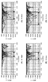
図8は、付加導体板の可変幅Wをそれぞれ4mm、6mm、8mm及び10mmとした場合に、付加導体板の長さL1とL2とをパラメータとして、それぞれ0mmから30mmまで5mm間隔で変更したときのリターンロスの変化を示してしている。なお、実施形態1の条件では幅Wが10mmである。このため、W=10mmの場合を示す図8(A)には、図5(B)に示した特性と同様の特性が示される。この時、良好な動作の目安となるリターンロスが−10dB以下となる周波数範囲はおおよそ50MHzである。 FIG. 8 shows the case where the length L1 and L2 of the additional conductor plate is changed from 0 mm to 30 mm at intervals of 5 mm when the variable width W of the additional conductor plate is 4 mm, 6 mm, 8 mm and 10 mm, respectively. The change in return loss is shown. Note that the width W is 10 mm under the conditions of the first embodiment. Therefore, FIG. 8A showing the case of W = 10 mm shows the same characteristics as the characteristics shown in FIG. At this time, the frequency range in which the return loss, which is a standard for good operation, is -10 dB or less is approximately 50 MHz.
実施形態1においては、ターゲットとなる共振周波数を固定していたため、周波数範囲がそれを含んでさえいればよかった。本実施形態では、単体特性での共振周波数から異なる値に周波数を変動させる事を想定し、この周波数範囲を拡大することを検討する。付加導体板の可変幅Wを8mmに狭めた場合では、L1、L2の設定を同様に行ったとしても、図8(B)に示すように、リターンロスが−10dB以下となる周波数範囲はおおよそ60MHzまで拡大することができる。さらに、可変幅Wを6mmに狭めた場合は、図8(C)に示すように、周波数範囲を80MHzまで拡大することができ、可変幅Wを4mmに狭めた場合は、図8(D)に示すように、周波数範囲を120MHzまで拡大することができる。よって、付加導体の長さだけでなく幅も調整可能として設定する事により、広範囲な周波数調整が可能となる。 In the first embodiment, since the target resonance frequency is fixed, the frequency range only needs to include it. In the present embodiment, it is assumed that the frequency is changed from a resonance frequency with a single characteristic to a different value, and it is considered to expand this frequency range. When the variable width W of the additional conductor plate is narrowed to 8 mm, even if L1 and L2 are set in the same manner, as shown in FIG. 8B, the frequency range in which the return loss is −10 dB or less is approximately It can be expanded to 60 MHz. Further, when the variable width W is narrowed to 6 mm, the frequency range can be expanded to 80 MHz as shown in FIG. 8C, and when the variable width W is narrowed to 4 mm, FIG. As shown, the frequency range can be expanded to 120 MHz. Accordingly, by setting not only the length of the additional conductor but also the width, it is possible to adjust a wide range of frequencies.
<<実施形態3>>
本実施形態では、実施形態1及び実施形態2と異なる実装条件においても、同様に共振周波数の調整を行う手法に関して説明する。実施形態3におけるパッチアンテナ素子101は、実施形態1及び実施形態2と同様、図1(b)に示す構成を有し、パッチアンテナ素子101単体での共振特性は、図2に示したようなものであるとする。
<< Embodiment 3 >>
In the present embodiment, a method for adjusting the resonance frequency in the same manner under the mounting conditions different from those in the first and second embodiments will be described. The
図9に、本実施形態で想定するアンテナ装置の実装条件の例を示す。本実装条件では、パッチアンテナ素子901の上面に120mm四方の金属板902があり、中心に10mm四方の開口部903がある。そして、この開口部の真下にパッチアンテナ素子901がちょうど収まる位置関係であり、パッチアンテナの上面と金属板の下面との距離は1mmであるものとする。この条件でのアンテナ特性を図10に示す。曲線1001で示される共振特性は、図2で示した共振特性から著しく劣化してしまっていることが分かる。
FIG. 9 shows an example of mounting conditions of the antenna device assumed in the present embodiment. Under this mounting condition, a 120 mm
そこで、本発明を適用した、実施形態3におけるアンテナ実装時の状態を図11に示す。図11(A)はアンテナ全体の形状を示し、本実施形態では、図6(A)と同様に、付加導体板102及び103をパッチアンテナ背面に垂直に延長した構造とする。また、2つの付加導体板102及び103の幅Wは共に6mmとする。図11(B)は、2つの付加導体板102及び103の長さL1及びL2を5mm〜30mmの間で5mm間隔で変更した際の、共振特性の変化を示している。図11(B)から、2つの付加導体板の長さを設定する事で、共振周波数の修正と共振の強さの回復が可能となることが分かる。そして、この設定の結果得られた最適な特性を、図12に示す。なお、この特性を得るために、付加導体板102の長さL1を10mm、付加導体板103の長さL2を30mmとしている。図12から、アンテナ形状を図11(A)のようにし、2つの板金の寸法を適切に設定する事により、周波数のずれと共振の劣化を共に回復する事が可能となる。
FIG. 11 shows a state when the antenna is mounted in the third embodiment to which the present invention is applied. FIG. 11A shows the shape of the entire antenna. In this embodiment, as in FIG. 6A, the
なお、上述の各実施形態では、パッチ導体105と同一の面にマイクロストリップ線路などの給電線104がある場合を説明したが、セラミックブロックを貫通する同軸ケーブルなどのピンをパッチ導体105に接続して給電するピン給電を用いてもよい。ピン給電の場合、ピンはパッチ導体105の中心からずれた箇所に接続されるが、ピンの接続箇所と中心とを結ぶ直線に直交ないしは略直交する方向に、付加導体板102及び103を追加する。すなわち、パッチ導体105内では、給電点とパッチ導体105の中心を結ぶ線に対して左右対称に電流が流れるところ、その左右方向に対して付加導体板を追加する。これにより、効率的に共振特性を補償し、目的のアンテナ特性を得ることが可能となる。
In each of the above-described embodiments, the case where the
Claims (5)
前記接地導体板に高周波結合されると共に、前記導体板の中心と前記給電点とを結ぶ直線に直交する方向に延びる形状を有する少なくとも1つの付加導体板と、
を有し、
金属が近接している第1の実装条件において、前記パッチアンテナ素子と、長さと幅と位置との少なくとも何れかを第1の値にした前記付加導体板とを用いて第1の共振周波数で動作し、
前記第1の実装条件とは異なる、金属が近接している第2の実装条件において、前記パッチアンテナ素子と、長さと幅と位置との少なくとも何れかを第2の値にした前記付加導体板とを用いて第1の共振周波数で動作する、
ことを特徴とするアンテナ装置。 And the conductor plate, possess a ground conductor plate provided opposite at a predetermined distance on one side of the conductor plate, and a feeding point that supplies power to the conductive plate, the at conditions which do not close the metal A patch antenna element operating at a resonance frequency of 1 ;
At least one additional conductor plate having a shape that is coupled to the ground conductor plate at a high frequency and extends in a direction perpendicular to a straight line connecting the center of the conductor plate and the feeding point;
I have a,
In the first mounting condition in which the metal is in close proximity, the patch antenna element and the additional conductor plate having at least one of the length, the width, and the position are set to a first resonance frequency. Work,
The additional conductor plate in which at least one of the patch antenna element and the length, width, and position is set to a second value in a second mounting condition that is different from the first mounting condition and in which the metal is in proximity. operating at a first resonant frequency using preparative,
Antenna device comprising a call.
ことを特徴とする請求項1に記載のアンテナ装置。 The additional conductor plate has a shape extending on a plane parallel to a plane including the ground conductor plate.
The antenna device according to claim 1.
ことを特徴とする請求項1に記載のアンテナ装置。 The additional conductor plate is in the direction of the normal line of the surface including the ground conductor plate and has a shape extending to the opposite side of the conductor plate.
The antenna device according to claim 1.
2つの前記付加導体板は、前記導体板の中心を含む前記導体板の法線に対して互いに軸対称となる位置から延びる形状を有する、
ことを特徴とする請求項1から3のいずれか1項に記載のアンテナ装置。 The antenna device has two additional conductor plates,
The two additional conductor plates have shapes extending from positions that are axially symmetric with respect to the normal line of the conductor plate including the center of the conductor plate.
The antenna device according to any one of claims 1 to 3, wherein
前記結合用領域と前記接地導体板とが張り合わされることにより、前記付加導体板と前記接地導体板とが高周波結合する、
ことを特徴とする請求項1から4のいずれか1項に記載のアンテナ装置。 The additional conductor plate has a coupling region for high-frequency coupling with the ground conductor plate,
The additional conductor plate and the ground conductor plate are high-frequency coupled by bonding the coupling region and the ground conductor plate,
The antenna device according to any one of claims 1 to 4, wherein:
Priority Applications (2)
| Application Number | Priority Date | Filing Date | Title |
|---|---|---|---|
| JP2012120139A JP5969821B2 (en) | 2012-05-25 | 2012-05-25 | Antenna device |
| US13/868,834 US20130314285A1 (en) | 2012-05-25 | 2013-04-23 | Antenna device and wireless communication apparatus |
Applications Claiming Priority (1)
| Application Number | Priority Date | Filing Date | Title |
|---|---|---|---|
| JP2012120139A JP5969821B2 (en) | 2012-05-25 | 2012-05-25 | Antenna device |
Publications (3)
| Publication Number | Publication Date |
|---|---|
| JP2013247526A JP2013247526A (en) | 2013-12-09 |
| JP2013247526A5 JP2013247526A5 (en) | 2015-07-09 |
| JP5969821B2 true JP5969821B2 (en) | 2016-08-17 |
Family
ID=49621193
Family Applications (1)
| Application Number | Title | Priority Date | Filing Date |
|---|---|---|---|
| JP2012120139A Active JP5969821B2 (en) | 2012-05-25 | 2012-05-25 | Antenna device |
Country Status (2)
| Country | Link |
|---|---|
| US (1) | US20130314285A1 (en) |
| JP (1) | JP5969821B2 (en) |
Families Citing this family (8)
| Publication number | Priority date | Publication date | Assignee | Title |
|---|---|---|---|---|
| JP6204747B2 (en) | 2013-08-21 | 2017-09-27 | キヤノン株式会社 | Electromagnetic band gap device and electronic circuit |
| JP2015185946A (en) | 2014-03-20 | 2015-10-22 | キヤノン株式会社 | antenna device |
| JP5848848B1 (en) * | 2015-07-07 | 2016-01-27 | パナソニック株式会社 | Antenna device |
| JP6958330B2 (en) | 2017-12-20 | 2021-11-02 | 富士通株式会社 | Antenna device and design program |
| JP7188050B2 (en) * | 2018-12-17 | 2022-12-13 | 富士通株式会社 | Antenna design support program, antenna design support device, and antenna design support method |
| JP7234732B2 (en) * | 2019-03-26 | 2023-03-08 | 株式会社Soken | antenna device |
| JP7279495B2 (en) * | 2019-04-26 | 2023-05-23 | 株式会社Soken | Vehicle communication device |
| TWI824273B (en) * | 2020-12-03 | 2023-12-01 | 仁寶電腦工業股份有限公司 | Antenna device and method for configuring the same |
Family Cites Families (10)
| Publication number | Priority date | Publication date | Assignee | Title |
|---|---|---|---|---|
| JP2525545Y2 (en) * | 1990-06-27 | 1997-02-12 | 日本電業工作株式会社 | Broadband microstrip antenna |
| US5652595A (en) * | 1995-05-04 | 1997-07-29 | Motorola, Inc. | Patch antenna including reactive loading |
| JPH10163738A (en) * | 1996-11-29 | 1998-06-19 | Matsushita Electric Ind Co Ltd | Surface mounted antenna and mounting method therefor |
| US20020126051A1 (en) * | 2000-11-09 | 2002-09-12 | Jha Asu Ram | Multi-purpose, ultra-wideband antenna |
| TW579077U (en) * | 2001-04-11 | 2004-03-01 | Wistron Neweb Corp | Tunable antenna for radio transceiver device |
| JP2003110351A (en) * | 2001-07-25 | 2003-04-11 | Denso Corp | Antenna apparatus |
| JP2004312533A (en) * | 2003-04-09 | 2004-11-04 | Alps Electric Co Ltd | Patch antenna apparatus |
| US20080252537A1 (en) * | 2007-04-10 | 2008-10-16 | Think Wireless, Inc. | Through-glass antenna system |
| JP2011096056A (en) * | 2009-10-30 | 2011-05-12 | Toppan Forms Co Ltd | Non-contact type data reception/transmission body |
| JP2011257986A (en) * | 2010-06-09 | 2011-12-22 | Toppan Forms Co Ltd | Non-contact type data reception/transmission body |
-
2012
- 2012-05-25 JP JP2012120139A patent/JP5969821B2/en active Active
-
2013
- 2013-04-23 US US13/868,834 patent/US20130314285A1/en not_active Abandoned
Also Published As
| Publication number | Publication date |
|---|---|
| JP2013247526A (en) | 2013-12-09 |
| US20130314285A1 (en) | 2013-11-28 |
Similar Documents
| Publication | Publication Date | Title |
|---|---|---|
| JP5969821B2 (en) | Antenna device | |
| US10056696B2 (en) | Antenna structure | |
| TWI425713B (en) | Three-band antenna device with resonance generation | |
| JP4384102B2 (en) | Portable radio device and antenna device | |
| US9590304B2 (en) | Broadband antenna | |
| US8779988B2 (en) | Surface mount device multiple-band antenna module | |
| JP6015944B2 (en) | ANTENNA DEVICE, COMMUNICATION DEVICE, AND ELECTRONIC DEVICE | |
| JP2013051644A (en) | Antenna device and electronic apparatus comprising the same | |
| EP2418728A1 (en) | Antenna arrangement, dielectric substrate, PCB & device | |
| US8963780B2 (en) | Antenna module | |
| CN108352621B (en) | Antenna device | |
| US10916847B2 (en) | Multi-band antenna | |
| JP2013074619A (en) | Electronic communication device and antenna structure | |
| US8319691B2 (en) | Multi-band antenna | |
| TW202306242A (en) | Antenna structure | |
| WO2013145623A1 (en) | Antenna unit and mobile wireless device equipped with same | |
| US9306274B2 (en) | Antenna device and antenna mounting method | |
| US9300037B2 (en) | Antenna device and antenna mounting method | |
| WO2018021353A1 (en) | Antenna and wireless module | |
| JP6865072B2 (en) | Antenna device and electronic device equipped with an antenna device | |
| JP6393048B2 (en) | Multiband antenna | |
| WO2016186092A1 (en) | Antenna device and electronic apparatus | |
| TWI530025B (en) | Multiband antenna for portable electronic device | |
| JP4833897B2 (en) | Dual frequency antenna | |
| WO2019198666A1 (en) | Antenna device |
Legal Events
| Date | Code | Title | Description |
|---|---|---|---|
| A521 | Written amendment |
Free format text: JAPANESE INTERMEDIATE CODE: A523 Effective date: 20150522 |
|
| A621 | Written request for application examination |
Free format text: JAPANESE INTERMEDIATE CODE: A621 Effective date: 20150522 |
|
| A977 | Report on retrieval |
Free format text: JAPANESE INTERMEDIATE CODE: A971007 Effective date: 20160304 |
|
| A131 | Notification of reasons for refusal |
Free format text: JAPANESE INTERMEDIATE CODE: A131 Effective date: 20160314 |
|
| A521 | Written amendment |
Free format text: JAPANESE INTERMEDIATE CODE: A523 Effective date: 20160509 |
|
| TRDD | Decision of grant or rejection written | ||
| A01 | Written decision to grant a patent or to grant a registration (utility model) |
Free format text: JAPANESE INTERMEDIATE CODE: A01 Effective date: 20160610 |
|
| A61 | First payment of annual fees (during grant procedure) |
Free format text: JAPANESE INTERMEDIATE CODE: A61 Effective date: 20160708 |
|
| R151 | Written notification of patent or utility model registration |
Ref document number: 5969821 Country of ref document: JP Free format text: JAPANESE INTERMEDIATE CODE: R151 |