JP5542902B2 - antenna - Google Patents
antenna Download PDFInfo
- Publication number
- JP5542902B2 JP5542902B2 JP2012260765A JP2012260765A JP5542902B2 JP 5542902 B2 JP5542902 B2 JP 5542902B2 JP 2012260765 A JP2012260765 A JP 2012260765A JP 2012260765 A JP2012260765 A JP 2012260765A JP 5542902 B2 JP5542902 B2 JP 5542902B2
- Authority
- JP
- Japan
- Prior art keywords
- antenna
- ebg structure
- pair
- elements
- square
- Prior art date
- Legal status (The legal status is an assumption and is not a legal conclusion. Google has not performed a legal analysis and makes no representation as to the accuracy of the status listed.)
- Active
Links
Images


Classifications
-
- H—ELECTRICITY
- H01—ELECTRIC ELEMENTS
- H01Q—ANTENNAS, i.e. RADIO AERIALS
- H01Q19/00—Combinations of primary active antenna elements and units with secondary devices, e.g. with quasi-optical devices, for giving the antenna a desired directional characteristic
- H01Q19/10—Combinations of primary active antenna elements and units with secondary devices, e.g. with quasi-optical devices, for giving the antenna a desired directional characteristic using reflecting surfaces
- H01Q19/108—Combination of a dipole with a plane reflecting surface
-
- H—ELECTRICITY
- H01—ELECTRIC ELEMENTS
- H01Q—ANTENNAS, i.e. RADIO AERIALS
- H01Q1/00—Details of, or arrangements associated with, antennas
- H01Q1/36—Structural form of radiating elements, e.g. cone, spiral, umbrella; Particular materials used therewith
- H01Q1/38—Structural form of radiating elements, e.g. cone, spiral, umbrella; Particular materials used therewith formed by a conductive layer on an insulating support
-
- H—ELECTRICITY
- H01—ELECTRIC ELEMENTS
- H01Q—ANTENNAS, i.e. RADIO AERIALS
- H01Q15/00—Devices for reflection, refraction, diffraction or polarisation of waves radiated from an antenna, e.g. quasi-optical devices
- H01Q15/0006—Devices acting selectively as reflecting surface, as diffracting or as refracting device, e.g. frequency filtering or angular spatial filtering devices
- H01Q15/006—Selective devices having photonic band gap materials or materials of which the material properties are frequency dependent, e.g. perforated substrates, high-impedance surfaces
-
- H—ELECTRICITY
- H01—ELECTRIC ELEMENTS
- H01Q—ANTENNAS, i.e. RADIO AERIALS
- H01Q15/00—Devices for reflection, refraction, diffraction or polarisation of waves radiated from an antenna, e.g. quasi-optical devices
- H01Q15/0006—Devices acting selectively as reflecting surface, as diffracting or as refracting device, e.g. frequency filtering or angular spatial filtering devices
- H01Q15/0086—Devices acting selectively as reflecting surface, as diffracting or as refracting device, e.g. frequency filtering or angular spatial filtering devices said selective devices having materials with a synthesized negative refractive index, e.g. metamaterials or left-handed materials
-
- H—ELECTRICITY
- H01—ELECTRIC ELEMENTS
- H01Q—ANTENNAS, i.e. RADIO AERIALS
- H01Q15/00—Devices for reflection, refraction, diffraction or polarisation of waves radiated from an antenna, e.g. quasi-optical devices
- H01Q15/14—Reflecting surfaces; Equivalent structures
- H01Q15/22—Reflecting surfaces; Equivalent structures functioning also as polarisation filter
-
- H—ELECTRICITY
- H01—ELECTRIC ELEMENTS
- H01Q—ANTENNAS, i.e. RADIO AERIALS
- H01Q21/00—Antenna arrays or systems
- H01Q21/24—Combinations of antenna units polarised in different directions for transmitting or receiving circularly and elliptically polarised waves or waves linearly polarised in any direction
-
- H—ELECTRICITY
- H01—ELECTRIC ELEMENTS
- H01Q—ANTENNAS, i.e. RADIO AERIALS
- H01Q5/00—Arrangements for simultaneous operation of antennas on two or more different wavebands, e.g. dual-band or multi-band arrangements
- H01Q5/30—Arrangements for providing operation on different wavebands
- H01Q5/378—Combination of fed elements with parasitic elements
-
- H—ELECTRICITY
- H01—ELECTRIC ELEMENTS
- H01Q—ANTENNAS, i.e. RADIO AERIALS
- H01Q9/00—Electrically-short antennas having dimensions not more than twice the operating wavelength and consisting of conductive active radiating elements
- H01Q9/04—Resonant antennas
- H01Q9/16—Resonant antennas with feed intermediate between the extremities of the antenna, e.g. centre-fed dipole
Description
本発明は、アンテナに係わり、特に、EBG(Electromagnetic Band Gap)構造体を反射板として使用するアンテナに関する。 The present invention relates to an antenna, and more particularly to an antenna that uses an EBG (Electromagnetic Band Gap) structure as a reflector.
天井など、屋内で使用されるアンテナとしては、設置や景観上の観点から、平面構造で薄型であることが求められる。
メタマテリアル技術を用いたEBG構造体を反射板として用いることにより、アンテナを低姿勢化することが可能である。
下記特許文献1には、EBG反射板上に配置された2周波対応アンテナが提案されている。
An antenna used indoors such as a ceiling is required to be thin and have a planar structure from the viewpoint of installation and landscape.
By using an EBG structure using metamaterial technology as a reflector, the antenna can be lowered.
しかしながら、EBG構造体は周波数依存性が高く狭帯域となるので、EBG構造体を反射板として使用するアンテナは、周波数特性が狭帯域になるという問題点があった。
本発明は、前記従来技術の問題点を解決するためになされたものであり、本発明の目的は、EBG構造体を有する反射板を用いて、低姿勢かつ広帯域な周波数特性を有するアンテナを提供することにある。
本発明の前記ならびにその他の目的と新規な特徴は、本明細書の記述及び添付図面によって明らかにする。
However, since the EBG structure has a high frequency dependency and a narrow band, an antenna using the EBG structure as a reflector has a problem that the frequency characteristic becomes a narrow band.
The present invention has been made to solve the problems of the prior art, and an object of the present invention is to provide an antenna having a low-profile and wide-band frequency characteristic using a reflector having an EBG structure. There is to do.
The above and other objects and novel features of the present invention will become apparent from the description of this specification and the accompanying drawings.
本願において開示される発明のうち、代表的なものの概要を簡単に説明すれば、下記の通りである。
(1)アンテナは、導電体と、前記導電体上に空気層を挟んでマトリクス状に配置される複数の正方形素子を有するEBG構造体と、前記EBG構造体上に配置される放射素子と、を備え、前記放射素子の設計中心周波数の波長をλoとするとき、前記導電体と前記EBG構造体との間隔L1は、0.01λo≦L1≦0.15λo、好ましくは、0.025λo≦L1≦0.085λo、より好ましくは、0.035λo≦L1≦0.07λoであり、前記EBG構造体における前記複数の正方形素子のそれぞれは、前記導電体及び当該複数の正方形素子における他の正方形素子のいずれにも直流的に接続されていない。
(2)(1)において、前記放射素子は、直線偏波を送受信する並列に配置された一対のダイポール素子と、直線偏波と直交する直線偏波を送受信する並列に配列された他の一対のダイポール素子と、を備え、前記一対のダイポール素子及び前記他の一対のダイポール素子は、当該一対のダイポール素子のそれぞれの中心を結ぶ線と当該他の一対のダイポール素子のそれぞれの中心を結ぶ線とが交差するように設けられている。
(3)(1)または(2)において、前記EBG構造体は、前記放射素子に対応する部分の正方形素子が取り除かれている。
(4)(1)ないし(3)のいずかにおいて、前記放射素子は、無給電素子を有する。
Of the inventions disclosed in this application, the outline of typical ones will be briefly described as follows.
(1) An antenna includes a conductor, an EBG structure having a plurality of square elements arranged in a matrix with an air layer interposed between the conductor, and a radiating element arranged on the EBG structure, When the wavelength of the design center frequency of the radiating element is λo, the distance L1 between the conductor and the EBG structure is 0.01λo ≦ L1 ≦ 0.15λo, preferably 0.025λo ≦ L1 ≦ 0.085λo, more preferably 0.035λo ≦ L1 ≦ 0.07λo , and each of the plurality of square elements in the EBG structure is the same as the other square elements in the conductor and the plurality of square elements. Neither is connected in a direct current manner .
(2) In (1), the radiating element includes a pair of dipole elements arranged in parallel for transmitting and receiving linearly polarized waves, and another pair arranged in parallel for transmitting and receiving linearly polarized waves orthogonal to the linearly polarized waves. The pair of dipole elements and the other pair of dipole elements are a line connecting the centers of the pair of dipole elements and the centers of the other pair of dipole elements. And are provided to cross.
( 3 ) In (1) or (2) , in the EBG structure, a square element corresponding to the radiating element is removed.
(4) In one (1) to (3) noise, said radiation element has a parasitic element.
本願において開示される発明のうち代表的なものによって得られる効果を簡単に説明すれば、下記の通りである。
本発明によれば、EBG構造体を有する反射板を用いて、低姿勢かつ広帯域な周波数特性を有するアンテナを提供することが可能となる。
The effects obtained by the representative ones of the inventions disclosed in the present application will be briefly described as follows.
ADVANTAGE OF THE INVENTION According to this invention, it becomes possible to provide the antenna which has a low profile and a wideband frequency characteristic using the reflecting plate which has an EBG structure.
以下、図面を参照して本発明の実施例を詳細に説明する。
なお、実施例を説明するための全図において、同一機能を有するものは同一符号を付け、その繰り返しの説明は省略する。また、以下の実施例は、本発明の特許請求の範囲の解釈を限定するためのものではない。
[実施例1]
図1ないし図4は、本発明の実施例1のアンテナの一例を説明するための図である。
図2は、本実施例のアンテナの断面図、
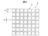
図3は、本実施例のアンテナのEBG構造体3の平面図、
図4は、本実施例のアンテナの放射素子2の平面図である。
本実施例のアンテナは、金属板から成る反射板1と、反射板1上に配置されるEBG(Electromagnetic Band Gap)構造体3と、EBG構造体3上に配置される放射素子2とを有する。
図2に示すように、放射素子2は、垂直偏波用の一対のダイポールアンテナ21と、水平偏波用の一対のダイポールアンテナ22とで構成される。ここで、垂直偏波用の一対のダイポールアンテナ素子21と、水平偏波用の一対のダイポールアンテナ22は、誘電基板上にプリント配線技術で形成してもよく、あるいは、金属の棒、管などを使用してもよい。
なお、放射素子2として、例えば、垂直偏波用のパッチアンテナ、水平偏波用のパッチアンテナ、あるいは、偏波共用のパッチアンテナを使用することも可能である。
Hereinafter, embodiments of the present invention will be described in detail with reference to the drawings.
In all the drawings for explaining the embodiments, parts having the same functions are given the same reference numerals, and repeated explanation thereof is omitted. Also, the following examples are not intended to limit the interpretation of the scope of the claims of the present invention.
[Example 1]
1 to 4 are diagrams for explaining an example of the antenna according to the first embodiment of the present invention.
FIG. 2 is a cross-sectional view of the antenna of the present embodiment.
FIG. 3 is a plan view of the
FIG. 4 is a plan view of the
The antenna of the present embodiment includes a
As shown in FIG. 2, the
As the
図3に示すように、EBG構造体3は、マトリクス状に配置される(7×7)個の正方形素子31を有する。ここで、EBG構造体3は、誘電基板上にプリント配線技術で形成してもよく、あるいは、金属の板などを使用してもよい。
なお、マトリクス状に配置される正方形素子31の数は、要求される指向特性によって増減することができる。
EBG構造体3は、核となる正方形素子31のインダクタンスと、隣接する正方形素子31との間でキャパシタンスを形成するため、固有のインピーダンス面を作り出す。そして、EBG構造体3の正方形素子31の大きさと間隔を適切に選ぶことにより適切なインピーダンス面を実現し、大きな効果を得ることができる。
本実施例において、アンテナの設計中心周波数foの自由空間波長をλoとするとき、反射板1とEBG構造体3との間隔(図2のL1)は、0.05λoであり、反射板1と放射素子2との間隔(図2のL2)は、0.1λoである。
また、反射板1の一辺の長さ(図2のL3)は、1.52λoである。
また、EBG構造体3の正方形素子31の一辺の長さ(図3のL4)は、0.2λoであり、隣接する正方形素子31との間隔(図3のL5)は、0.02λoである。
さらに、放射素子2を構成する垂直偏波用の一対のダイポールアンテナ素子21および水平偏波用の一対のダイポールアンテナ22の幅(図4のL6)は、0.12λo、垂直偏波用の一対のダイポールアンテナ素子21および水平偏波用の一対のダイポールアンテナ22の長さ(図4のL7)は、0.46λo、垂直偏波用の一対のダイポールアンテナ素子21および水平偏波用の一対のダイポールアンテナ22の間隔(図4のL8)は、0.64λoである。
As shown in FIG. 3, the
Note that the number of
Since the
In this embodiment, when the free space wavelength of the design center frequency fo of the antenna is λo, the distance between the
Further, the length of one side (L3 in FIG. 2) of the
The length of one side (L4 in FIG. 3) of the
Further, the width (L6 in FIG. 4) of the pair of vertically polarized
図5は、本実施例のアンテナの反射減衰量(リターンロス)特性を示すグラフである。
図5から分かるように、本実施例のアンテナにおいて、反射減衰量が、−10dB以下となる周波数特性の比帯域幅(即ち、VSWR≦2となる周波数特性の比帯域幅)は、22.3%である。なお、図5のグラフでは、設計中心周波数foは、1.9GHz、設計中心周波数foの自由空間波長λoは、157.9mmである。
また、周波数特性の比帯域幅は、(fwide×100)/foで表される。ここで、fwideは、反射減衰量が、−10dB以下となる周波数帯域である。
図11は、本実施例のアンテナと比較するための、比較例のアンテナの反射減衰量(リターンロス)特性を示すグラフである。
図11に示す比較例のアンテナは、反射板1とEBG構造体3との間隔(図2のL1)が、0.006λoである以外は、本実施例のアンテナと仕様が同じである。
図11から分かるように、比較例のアンテナにおいて、反射減衰量が、−10dB以下となる周波数特性の比帯域幅(即ち、VSWR≦2となる周波数特性の比帯域幅)は、7.6%である。なお、図11のグラフでも、設計中心周波数foは、1.9GHz、設計中心周波数foの自由空間波長λoは、157.9mmである。
FIG. 5 is a graph showing the return loss characteristics of the antenna of this example.
As can be seen from FIG. 5, in the antenna of this example, the specific bandwidth of the frequency characteristic where the return loss is −10 dB or less (that is, the specific bandwidth of the frequency characteristic satisfying VSWR ≦ 2) is 22.3. %. In the graph of FIG. 5, the design center frequency fo is 1.9 GHz, and the free space wavelength λo of the design center frequency fo is 157.9 mm.
The specific bandwidth of the frequency characteristic is represented by (fwide × 100) / fo. Here, fwide is a frequency band in which the return loss is -10 dB or less.
FIG. 11 is a graph showing the return loss characteristic of the antenna of the comparative example for comparison with the antenna of the present embodiment.
The antenna of the comparative example shown in FIG. 11 has the same specifications as the antenna of the present embodiment, except that the distance between the
As can be seen from FIG. 11, in the antenna of the comparative example, the specific bandwidth of the frequency characteristic where the return loss is −10 dB or less (that is, the specific bandwidth of the frequency characteristic satisfying VSWR ≦ 2) is 7.6%. It is. In the graph of FIG. 11, the design center frequency fo is 1.9 GHz, and the free space wavelength λo of the design center frequency fo is 157.9 mm.
このように、本実施例では、反射板1とEBG構造体3との間隔(図2のL1)を広げることにより、周波数特性を広げることができるので、本実施例によれば、低姿勢かつ広帯域な周波数特性を有するアンテナを提供することが可能となる。
図6は、本実施例のアンテナにおいて、放射素子2とEBG構造体3との間隔(図2のL2−L1)を一定(0.05λo)にして、反射板1と放射素子2との間隔(図2のL2)を変化させたときに、反射減衰量が、−10dBとなる比帯域幅の変化を示すグラフである。
図6に示すグラフから、本実施例のアンテナにおいて、広帯域な周波数特性を実現するためには、反射板1とEBG構造体3との間隔(図2のL1)は、0.01λo≦L1≦0.15λo、好ましくは、0.025λo≦L1≦0.085λo、より好ましくは、0.035λo≦L1≦0.07λoが望ましい。
As described above, in this embodiment, the frequency characteristics can be widened by widening the distance between the
FIG. 6 shows the distance between the
From the graph shown in FIG. 6, in order to realize a wide frequency characteristic in the antenna of this embodiment, the distance between the
[実施例2]
図7は、本実施例のアンテナの放射素子2の平面図である。
本発明の実施例2のアンテナは、図7に示すように、放射素子2を構成する、垂直偏波用の一対のダイポールアンテナ21と、水平偏波用の一対のダイポールアンテナ22とが無給電素子5を有する点で、前述の実施例1のアンテナと相違する。
図7において、無給電素子5の幅(図7のL10)は、0.18λo、無給電素子5の長さ(図7のL9)は、0.25λoである。
図8は、本実施例のアンテナの反射減衰量(リターンロス)特性を示すグラフである。
図8から分かるように、本実施例のアンテナにおいて、反射減衰量が、−10dB以下となる周波数特性の比帯域幅(即ち、VSWR≦2となる周波数特性の比帯域幅)は、58.2%である。なお、図8のグラフでは、設計中心周波数foは、1.9GHz、設計中心周波数foの自由空間波長λoは、157.9mmである。
このように、前述の実施例1のアンテナにおいて、放射素子2を構成する、垂直偏波用の一対のダイポールアンテナ21と、水平偏波用の一対のダイポールアンテナ22に、無給電素子5を設けることにより、前述の実施例1のアンテナと比して、より広帯域な周波数特性を実現することが可能となる。
[Example 2]
FIG. 7 is a plan view of the radiating
As shown in FIG. 7, the antenna according to the second embodiment of the present invention includes a pair of vertically polarized
In FIG. 7, the width of parasitic element 5 (L10 in FIG. 7) is 0.18λo, and the length of parasitic element 5 (L9 in FIG. 7) is 0.25λo.
FIG. 8 is a graph showing the return loss characteristics of the antenna of this example.
As can be seen from FIG. 8, in the antenna of this example, the specific bandwidth of the frequency characteristic where the return loss is −10 dB or less (that is, the specific bandwidth of the frequency characteristic satisfying VSWR ≦ 2) is 58.2. %. In the graph of FIG. 8 , the design center frequency fo is 1.9 GHz, and the free space wavelength λo of the design center frequency fo is 157.9 mm.
As described above, the
[実施例3]
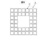
図9は、本発明の実施例3のアンテナのEBG構造体の平面図である。
本発明の実施例3のアンテナは、図9に示すように、EBG構造体3の中央の9(=3×3)個の正方形素子31を取り除いた点で、前述の実施例2のアンテナと相違する。
図10は、本発明の実施例3のアンテナの反射減衰量特性を示すグラフである。
図10から分かるように、本実施例のアンテナにおいて、反射減衰量が、−10dB以下となる周波数特性の比帯域幅(即ち、VSWR≦2となる周波数特性の比帯域幅)は、52.8%である。なお、図10のグラフでは、設計中心周波数foは、1.9GHz、設計中心周波数foの自由空間波長λoは、157.9mmである。
このように、前述の実施例2のアンテナにおいて、EBG構造体3の中央の9(=3×3)個の正方形素子31を取り除くことにより、前述の実施例2のアンテナと比して、周波数特性の比帯域幅は若干狭くなるが、EBG構造体3の中央の9(=3×3)個の正方形素子31を取り除いた箇所に、給電ラインを引き回すことができるので、本実施例では、前述の実施例2に比して、放射素子2を構成する、垂直偏波用の一対のダイポールアンテナ21と、水平偏波用の一対のダイポールアンテナ22に対する給電が容易となる。
なお、前述の実施例1のアンテナにおいても、EBG構造体3の中央の9(=3×3)個の正方形素子31を取り除くことが可能である。
以上、本発明者によってなされた発明を、前記実施例に基づき具体的に説明したが、本発明は、前記実施例に限定されるものではなく、その要旨を逸脱しない範囲において種々変更可能であることは勿論である。
[Example 3]
FIG. 9 is a plan view of the EBG structure of the antenna according to the third embodiment of the present invention.
As shown in FIG. 9, the antenna of the third embodiment of the present invention is different from the antenna of the second embodiment described above in that 9 (= 3 × 3)
FIG. 10 is a graph showing the return loss characteristics of the antenna according to Example 3 of the present invention.
As can be seen from FIG. 10, in the antenna of this example, the specific bandwidth of the frequency characteristics where the return loss is −10 dB or less (that is, the specific bandwidth of the frequency characteristics satisfying VSWR ≦ 2) is 52.8. %. In the graph of FIG. 10 , the design center frequency fo is 1.9 GHz, and the free space wavelength λo of the design center frequency fo is 157.9 mm.
Thus, in the antenna of the above-described second embodiment, by removing the 9 (= 3 × 3)
In the antenna of the first embodiment, it is possible to remove 9 (= 3 × 3)
As mentioned above, the invention made by the present inventor has been specifically described based on the above embodiments. However, the present invention is not limited to the above embodiments, and various modifications can be made without departing from the scope of the invention. Of course.
1 反射板
2 放射素子
3 EBG(Electromagnetic Band Gap)構造体
5 無給電素子
21 垂直偏波用の一対のダイポールアンテナ
22 水平偏波用の一対のダイポールアンテナ
31 正方形素子
DESCRIPTION OF
Claims (6)
前記導電体上に空気層を挟んでマトリクス状に配置される複数の正方形素子を有するEBG構造体と、
前記EBG構造体上に配置される放射素子と、を備え、
前記放射素子の設計中心周波数の波長をλoとするとき、
前記導電体と前記EBG構造体との間隔L1は、0.01λo≦L1≦0.15λoであり、
前記EBG構造体における前記複数の正方形素子のそれぞれは、前記導電体及び当該複数の正方形素子における他の正方形素子のいずれにも直流的に接続されていないことを特徴とするアンテナ。 A conductor;
An EBG structure having a plurality of square elements arranged in a matrix with an air layer interposed on the conductor;
And a radiating element disposed on said EBG structure,
When the wavelength of the design center frequency of the radiating element is λo,
An interval L1 between the conductor and the EBG structure is 0.01λo ≦ L1 ≦ 0.15λo ,
Wherein each of said plurality of square elements in EBG structure, an antenna, characterized in that not DC connected to any other of the square element in the conductor and the plurality of square elements.
前記一対のダイポール素子及び前記他の一対のダイポール素子は、当該一対のダイポール素子のそれぞれの中心を結ぶ線と当該他の一対のダイポール素子のそれぞれの中心を結ぶ線とが交差するように設けられていることを特徴とする請求項1に記載のアンテナ。The pair of dipole elements and the other pair of dipole elements are provided such that a line connecting the centers of the pair of dipole elements intersects a line connecting the centers of the other pair of dipole elements. The antenna according to claim 1.
Priority Applications (6)
| Application Number | Priority Date | Filing Date | Title |
|---|---|---|---|
| JP2012260765A JP5542902B2 (en) | 2012-11-29 | 2012-11-29 | antenna |
| EP13859315.7A EP2928018A4 (en) | 2012-11-29 | 2013-11-14 | Antenna |
| US14/442,006 US20150325923A1 (en) | 2012-11-29 | 2013-11-14 | Antenna |
| PCT/JP2013/080767 WO2014084058A1 (en) | 2012-11-29 | 2013-11-14 | Antenna |
| CN201380056372.XA CN104798256B (en) | 2012-11-29 | 2013-11-14 | Antenna |
| PH12015501136A PH12015501136A1 (en) | 2012-11-29 | 2015-05-21 | Antenna |
Applications Claiming Priority (1)
| Application Number | Priority Date | Filing Date | Title |
|---|---|---|---|
| JP2012260765A JP5542902B2 (en) | 2012-11-29 | 2012-11-29 | antenna |
Publications (2)
| Publication Number | Publication Date |
|---|---|
| JP2014107782A JP2014107782A (en) | 2014-06-09 |
| JP5542902B2 true JP5542902B2 (en) | 2014-07-09 |
Family
ID=50827703
Family Applications (1)
| Application Number | Title | Priority Date | Filing Date |
|---|---|---|---|
| JP2012260765A Active JP5542902B2 (en) | 2012-11-29 | 2012-11-29 | antenna |
Country Status (6)
| Country | Link |
|---|---|
| US (1) | US20150325923A1 (en) |
| EP (1) | EP2928018A4 (en) |
| JP (1) | JP5542902B2 (en) |
| CN (1) | CN104798256B (en) |
| PH (1) | PH12015501136A1 (en) |
| WO (1) | WO2014084058A1 (en) |
Families Citing this family (6)
| Publication number | Priority date | Publication date | Assignee | Title |
|---|---|---|---|---|
| JP5974057B2 (en) * | 2014-09-08 | 2016-08-23 | 電気興業株式会社 | Thin antenna |
| JP7015054B2 (en) * | 2018-04-03 | 2022-02-02 | 学校法人金沢工業大学 | Power converter and folded dipole antenna |
| JP7217429B2 (en) * | 2019-03-29 | 2023-02-03 | パナソニックIpマネジメント株式会社 | antenna device |
| CN111403907B (en) * | 2020-03-23 | 2021-05-04 | 西安电子科技大学 | Broadband low-profile circularly polarized antenna based on asymmetric dipole |
| JP7182137B2 (en) * | 2020-07-31 | 2022-12-02 | パナソニックIpマネジメント株式会社 | Antenna device and communication device |
| US20220102857A1 (en) * | 2020-09-29 | 2022-03-31 | T-Mobile Usa, Inc. | Multi-band millimeter wave (mmw) antenna arrays |
Family Cites Families (18)
| Publication number | Priority date | Publication date | Assignee | Title |
|---|---|---|---|---|
| JP2506015B2 (en) * | 1991-11-22 | 1996-06-12 | 日本無線株式会社 | Spiral antenna |
| US6768476B2 (en) * | 2001-12-05 | 2004-07-27 | Etenna Corporation | Capacitively-loaded bent-wire monopole on an artificial magnetic conductor |
| JP4057494B2 (en) * | 2003-08-29 | 2008-03-05 | 日本アンテナ株式会社 | Spiral antenna |
| JP2005094360A (en) | 2003-09-17 | 2005-04-07 | Kyocera Corp | Antenna device and radio communication apparatus |
| JP4288141B2 (en) * | 2003-11-18 | 2009-07-01 | 三井造船株式会社 | Gas hydrate transport ship |
| US7626216B2 (en) * | 2005-10-21 | 2009-12-01 | Mckinzie Iii William E | Systems and methods for electromagnetic noise suppression using hybrid electromagnetic bandgap structures |
| CN101542838B (en) * | 2006-08-25 | 2013-03-13 | 泰科电子服务有限责任公司 | Antennas based on metamaterial structures |
| WO2008050441A1 (en) * | 2006-10-26 | 2008-05-02 | Panasonic Corporation | Antenna device |
| WO2008148569A2 (en) * | 2007-06-06 | 2008-12-11 | Fractus, S.A. | Dual-polarized radiating element, dual-band dual-polarized antenna assembly and dual-polarized antenna array |
| JP2009033324A (en) * | 2007-07-25 | 2009-02-12 | Nippon Antenna Co Ltd | Antenna |
| JP4568355B2 (en) * | 2007-09-26 | 2010-10-27 | 株式会社日本自動車部品総合研究所 | Antenna device |
| US7855689B2 (en) * | 2007-09-26 | 2010-12-21 | Nippon Soken, Inc. | Antenna apparatus for radio communication |
| JP2009135797A (en) * | 2007-11-30 | 2009-06-18 | Toshiba Corp | Antenna apparatus |
| US8354975B2 (en) * | 2007-12-26 | 2013-01-15 | Nec Corporation | Electromagnetic band gap element, and antenna and filter using the same |
| WO2010029770A1 (en) * | 2008-09-11 | 2010-03-18 | 日本電気株式会社 | Structure, antenna, communication device, and electronic component |
| CN102349192B (en) * | 2009-03-30 | 2015-06-10 | 日本电气株式会社 | Resonator antenna |
| US8451189B1 (en) * | 2009-04-15 | 2013-05-28 | Herbert U. Fluhler | Ultra-wide band (UWB) artificial magnetic conductor (AMC) metamaterials for electrically thin antennas and arrays |
| CN102414920B (en) * | 2009-04-30 | 2016-06-08 | 日本电气株式会社 | Structure, printed panel, antenna, transmission line waveguide transducer, array antenna and electronic installation |
-
2012
- 2012-11-29 JP JP2012260765A patent/JP5542902B2/en active Active
-
2013
- 2013-11-14 WO PCT/JP2013/080767 patent/WO2014084058A1/en active Application Filing
- 2013-11-14 CN CN201380056372.XA patent/CN104798256B/en not_active Expired - Fee Related
- 2013-11-14 EP EP13859315.7A patent/EP2928018A4/en not_active Withdrawn
- 2013-11-14 US US14/442,006 patent/US20150325923A1/en not_active Abandoned
-
2015
- 2015-05-21 PH PH12015501136A patent/PH12015501136A1/en unknown
Also Published As
| Publication number | Publication date |
|---|---|
| EP2928018A1 (en) | 2015-10-07 |
| WO2014084058A1 (en) | 2014-06-05 |
| PH12015501136A1 (en) | 2015-08-03 |
| EP2928018A4 (en) | 2016-07-13 |
| US20150325923A1 (en) | 2015-11-12 |
| CN104798256A (en) | 2015-07-22 |
| CN104798256B (en) | 2016-05-11 |
| JP2014107782A (en) | 2014-06-09 |
Similar Documents
| Publication | Publication Date | Title |
|---|---|---|
| US8723751B2 (en) | Antenna system with planar dipole antennas and electronic apparatus having the same | |
| JP5542902B2 (en) | antenna | |
| US10418691B2 (en) | Antenna device for a base station antenna system | |
| JP6297337B2 (en) | Antenna assembly and communication device including the antenna assembly | |
| WO2016206388A1 (en) | Antenna element for signals with three polarizations | |
| US9515387B2 (en) | Multi-input multi-output antenna with electromagnetic band-gap structure | |
| US8174458B2 (en) | Dual-feed antenna | |
| US20120056790A1 (en) | Multi-loop antenna system and electronic apparatus having the same | |
| JP2015185946A (en) | antenna device | |
| US8648762B2 (en) | Loop array antenna system and electronic apparatus having the same | |
| WO2008156429A1 (en) | Broadband antenna for wireless communications | |
| CN105322291A (en) | Microstrip array antenna | |
| EP2833475A1 (en) | Dipole antenna | |
| EP3032644A1 (en) | Dipole antenna | |
| US10916848B2 (en) | Antenna | |
| KR20140018620A (en) | Micro-miniature antenna having dual-polarization | |
| KR102267314B1 (en) | Resonant cavity antenna | |
| JP2005203971A (en) | Antenna device and system | |
| KR100973489B1 (en) | Intenna for adjusting beam directivity degree | |
| JP5858844B2 (en) | Antenna device | |
| US10727585B2 (en) | Directional monopole array antenna using hybrid type ground plane | |
| JP2006191331A (en) | Antenna | |
| US11916293B2 (en) | Antenna structure and wireless communication device | |
| KR101284228B1 (en) | Dual-band array antenna using modified sierpinski fractal structure | |
| CN106654550B (en) | Zero-order resonant antenna and wireless router |
Legal Events
| Date | Code | Title | Description |
|---|---|---|---|
| A521 | Request for written amendment filed |
Free format text: JAPANESE INTERMEDIATE CODE: A523 Effective date: 20140314 |
|
| TRDD | Decision of grant or rejection written | ||
| A01 | Written decision to grant a patent or to grant a registration (utility model) |
Free format text: JAPANESE INTERMEDIATE CODE: A01 Effective date: 20140430 |
|
| A61 | First payment of annual fees (during grant procedure) |
Free format text: JAPANESE INTERMEDIATE CODE: A61 Effective date: 20140507 |
|
| R150 | Certificate of patent or registration of utility model |
Ref document number: 5542902 Country of ref document: JP Free format text: JAPANESE INTERMEDIATE CODE: R150 |
|
| R250 | Receipt of annual fees |
Free format text: JAPANESE INTERMEDIATE CODE: R250 |
|
| R250 | Receipt of annual fees |
Free format text: JAPANESE INTERMEDIATE CODE: R250 |
|
| S531 | Written request for registration of change of domicile |
Free format text: JAPANESE INTERMEDIATE CODE: R313531 |
|
| R350 | Written notification of registration of transfer |
Free format text: JAPANESE INTERMEDIATE CODE: R350 |
|
| R250 | Receipt of annual fees |
Free format text: JAPANESE INTERMEDIATE CODE: R250 |
|
| R250 | Receipt of annual fees |
Free format text: JAPANESE INTERMEDIATE CODE: R250 |