EP2915191B1 - Method of fabricating a conductive interconnect with an inorganic collar - Google Patents
Method of fabricating a conductive interconnect with an inorganic collar Download PDFInfo
- Publication number
- EP2915191B1 EP2915191B1 EP13795327.9A EP13795327A EP2915191B1 EP 2915191 B1 EP2915191 B1 EP 2915191B1 EP 13795327 A EP13795327 A EP 13795327A EP 2915191 B1 EP2915191 B1 EP 2915191B1
- Authority
- EP
- European Patent Office
- Prior art keywords
- conductive
- layer
- collar
- organic
- seed layer
- Prior art date
- Legal status (The legal status is an assumption and is not a legal conclusion. Google has not performed a legal analysis and makes no representation as to the accuracy of the status listed.)
- Active
Links
- 238000004519 manufacturing process Methods 0.000 title claims description 10
- 238000000034 method Methods 0.000 claims description 86
- 239000004020 conductor Substances 0.000 claims description 68
- 230000008569 process Effects 0.000 claims description 59
- 239000000758 substrate Substances 0.000 claims description 46
- 239000003989 dielectric material Substances 0.000 claims description 33
- 239000004065 semiconductor Substances 0.000 claims description 33
- 229920002120 photoresistant polymer Polymers 0.000 claims description 20
- 238000000151 deposition Methods 0.000 claims description 16
- 239000000463 material Substances 0.000 claims description 15
- 238000005530 etching Methods 0.000 claims description 9
- 238000000059 patterning Methods 0.000 claims description 8
- 238000004891 communication Methods 0.000 claims description 7
- 230000007704 transition Effects 0.000 claims description 5
- 238000010438 heat treatment Methods 0.000 claims description 3
- 230000004888 barrier function Effects 0.000 claims description 2
- 239000010949 copper Substances 0.000 description 35
- RYGMFSIKBFXOCR-UHFFFAOYSA-N Copper Chemical group [Cu] RYGMFSIKBFXOCR-UHFFFAOYSA-N 0.000 description 33
- 229910052802 copper Inorganic materials 0.000 description 33
- 229910000679 solder Inorganic materials 0.000 description 23
- 238000010586 diagram Methods 0.000 description 14
- VYPSYNLAJGMNEJ-UHFFFAOYSA-N Silicium dioxide Chemical compound O=[Si]=O VYPSYNLAJGMNEJ-UHFFFAOYSA-N 0.000 description 10
- PXHVJJICTQNCMI-UHFFFAOYSA-N Nickel Chemical compound [Ni] PXHVJJICTQNCMI-UHFFFAOYSA-N 0.000 description 9
- 230000006870 function Effects 0.000 description 8
- 230000015654 memory Effects 0.000 description 7
- 238000007747 plating Methods 0.000 description 7
- 238000009713 electroplating Methods 0.000 description 6
- 229910010272 inorganic material Inorganic materials 0.000 description 6
- 239000011147 inorganic material Substances 0.000 description 6
- 239000002184 metal Substances 0.000 description 6
- 229910052751 metal Inorganic materials 0.000 description 6
- 239000000203 mixture Substances 0.000 description 6
- 238000003860 storage Methods 0.000 description 6
- 238000006243 chemical reaction Methods 0.000 description 5
- 239000011368 organic material Substances 0.000 description 5
- 239000000377 silicon dioxide Substances 0.000 description 5
- 230000008901 benefit Effects 0.000 description 4
- 239000010931 gold Substances 0.000 description 4
- 238000007669 thermal treatment Methods 0.000 description 4
- 229910052738 indium Inorganic materials 0.000 description 3
- APFVFJFRJDLVQX-UHFFFAOYSA-N indium atom Chemical compound [In] APFVFJFRJDLVQX-UHFFFAOYSA-N 0.000 description 3
- 229910052759 nickel Inorganic materials 0.000 description 3
- ATJFFYVFTNAWJD-UHFFFAOYSA-N Tin Chemical compound [Sn] ATJFFYVFTNAWJD-UHFFFAOYSA-N 0.000 description 2
- 230000015572 biosynthetic process Effects 0.000 description 2
- 229910052797 bismuth Inorganic materials 0.000 description 2
- JCXGWMGPZLAOME-UHFFFAOYSA-N bismuth atom Chemical compound [Bi] JCXGWMGPZLAOME-UHFFFAOYSA-N 0.000 description 2
- 230000008859 change Effects 0.000 description 2
- 230000006835 compression Effects 0.000 description 2
- 238000007906 compression Methods 0.000 description 2
- 238000005516 engineering process Methods 0.000 description 2
- PCHJSUWPFVWCPO-UHFFFAOYSA-N gold Chemical compound [Au] PCHJSUWPFVWCPO-UHFFFAOYSA-N 0.000 description 2
- 229910052737 gold Inorganic materials 0.000 description 2
- 230000007246 mechanism Effects 0.000 description 2
- 230000003287 optical effect Effects 0.000 description 2
- 230000009467 reduction Effects 0.000 description 2
- 229910052710 silicon Inorganic materials 0.000 description 2
- 239000010703 silicon Substances 0.000 description 2
- 235000012239 silicon dioxide Nutrition 0.000 description 2
- BQCADISMDOOEFD-UHFFFAOYSA-N Silver Chemical compound [Ag] BQCADISMDOOEFD-UHFFFAOYSA-N 0.000 description 1
- 229910045601 alloy Inorganic materials 0.000 description 1
- 239000000956 alloy Substances 0.000 description 1
- 230000004075 alteration Effects 0.000 description 1
- 238000003491 array Methods 0.000 description 1
- 230000005540 biological transmission Effects 0.000 description 1
- 238000005229 chemical vapour deposition Methods 0.000 description 1
- 150000001875 compounds Chemical class 0.000 description 1
- 238000004590 computer program Methods 0.000 description 1
- 230000001419 dependent effect Effects 0.000 description 1
- 239000012776 electronic material Substances 0.000 description 1
- 230000017525 heat dissipation Effects 0.000 description 1
- 230000007774 longterm Effects 0.000 description 1
- 238000000465 moulding Methods 0.000 description 1
- 230000008520 organization Effects 0.000 description 1
- 238000004806 packaging method and process Methods 0.000 description 1
- 239000002243 precursor Substances 0.000 description 1
- 229910052709 silver Inorganic materials 0.000 description 1
- 239000004332 silver Substances 0.000 description 1
- 239000007787 solid Substances 0.000 description 1
- 238000006467 substitution reaction Methods 0.000 description 1
Images


Classifications
-
- H—ELECTRICITY
- H01—ELECTRIC ELEMENTS
- H01L—SEMICONDUCTOR DEVICES NOT COVERED BY CLASS H10
- H01L24/00—Arrangements for connecting or disconnecting semiconductor or solid-state bodies; Methods or apparatus related thereto
- H01L24/01—Means for bonding being attached to, or being formed on, the surface to be connected, e.g. chip-to-package, die-attach, "first-level" interconnects; Manufacturing methods related thereto
- H01L24/02—Bonding areas ; Manufacturing methods related thereto
- H01L24/03—Manufacturing methods
-
- H—ELECTRICITY
- H10—SEMICONDUCTOR DEVICES; ELECTRIC SOLID-STATE DEVICES NOT OTHERWISE PROVIDED FOR
- H10D—INORGANIC ELECTRIC SEMICONDUCTOR DEVICES
- H10D64/00—Electrodes of devices having potential barriers
- H10D64/60—Electrodes characterised by their materials
-
- B—PERFORMING OPERATIONS; TRANSPORTING
- B81—MICROSTRUCTURAL TECHNOLOGY
- B81C—PROCESSES OR APPARATUS SPECIALLY ADAPTED FOR THE MANUFACTURE OR TREATMENT OF MICROSTRUCTURAL DEVICES OR SYSTEMS
- B81C1/00—Manufacture or treatment of devices or systems in or on a substrate
- B81C1/00015—Manufacture or treatment of devices or systems in or on a substrate for manufacturing microsystems
- B81C1/00261—Processes for packaging MEMS devices
- B81C1/00269—Bonding of solid lids or wafers to the substrate
-
- H—ELECTRICITY
- H01—ELECTRIC ELEMENTS
- H01L—SEMICONDUCTOR DEVICES NOT COVERED BY CLASS H10
- H01L21/00—Processes or apparatus adapted for the manufacture or treatment of semiconductor or solid state devices or of parts thereof
- H01L21/70—Manufacture or treatment of devices consisting of a plurality of solid state components formed in or on a common substrate or of parts thereof; Manufacture of integrated circuit devices or of parts thereof
- H01L21/71—Manufacture of specific parts of devices defined in group H01L21/70
- H01L21/768—Applying interconnections to be used for carrying current between separate components within a device comprising conductors and dielectrics
-
- H—ELECTRICITY
- H01—ELECTRIC ELEMENTS
- H01L—SEMICONDUCTOR DEVICES NOT COVERED BY CLASS H10
- H01L23/00—Details of semiconductor or other solid state devices
- H01L23/48—Arrangements for conducting electric current to or from the solid state body in operation, e.g. leads, terminal arrangements ; Selection of materials therefor
- H01L23/488—Arrangements for conducting electric current to or from the solid state body in operation, e.g. leads, terminal arrangements ; Selection of materials therefor consisting of soldered or bonded constructions
- H01L23/498—Leads, i.e. metallisations or lead-frames on insulating substrates, e.g. chip carriers
- H01L23/49811—Additional leads joined to the metallisation on the insulating substrate, e.g. pins, bumps, wires, flat leads
-
- H—ELECTRICITY
- H01—ELECTRIC ELEMENTS
- H01L—SEMICONDUCTOR DEVICES NOT COVERED BY CLASS H10
- H01L24/00—Arrangements for connecting or disconnecting semiconductor or solid-state bodies; Methods or apparatus related thereto
- H01L24/01—Means for bonding being attached to, or being formed on, the surface to be connected, e.g. chip-to-package, die-attach, "first-level" interconnects; Manufacturing methods related thereto
- H01L24/10—Bump connectors ; Manufacturing methods related thereto
- H01L24/11—Manufacturing methods
-
- H—ELECTRICITY
- H01—ELECTRIC ELEMENTS
- H01L—SEMICONDUCTOR DEVICES NOT COVERED BY CLASS H10
- H01L24/00—Arrangements for connecting or disconnecting semiconductor or solid-state bodies; Methods or apparatus related thereto
- H01L24/01—Means for bonding being attached to, or being formed on, the surface to be connected, e.g. chip-to-package, die-attach, "first-level" interconnects; Manufacturing methods related thereto
- H01L24/10—Bump connectors ; Manufacturing methods related thereto
- H01L24/12—Structure, shape, material or disposition of the bump connectors prior to the connecting process
- H01L24/13—Structure, shape, material or disposition of the bump connectors prior to the connecting process of an individual bump connector
-
- H—ELECTRICITY
- H10—SEMICONDUCTOR DEVICES; ELECTRIC SOLID-STATE DEVICES NOT OTHERWISE PROVIDED FOR
- H10D—INORGANIC ELECTRIC SEMICONDUCTOR DEVICES
- H10D48/00—Individual devices not covered by groups H10D1/00 - H10D44/00
- H10D48/50—Devices controlled by mechanical forces, e.g. pressure
-
- B—PERFORMING OPERATIONS; TRANSPORTING
- B81—MICROSTRUCTURAL TECHNOLOGY
- B81B—MICROSTRUCTURAL DEVICES OR SYSTEMS, e.g. MICROMECHANICAL DEVICES
- B81B2207/00—Microstructural systems or auxiliary parts thereof
- B81B2207/09—Packages
- B81B2207/091—Arrangements for connecting external electrical signals to mechanical structures inside the package
- B81B2207/093—Conductive package seal
-
- B—PERFORMING OPERATIONS; TRANSPORTING
- B81—MICROSTRUCTURAL TECHNOLOGY
- B81C—PROCESSES OR APPARATUS SPECIALLY ADAPTED FOR THE MANUFACTURE OR TREATMENT OF MICROSTRUCTURAL DEVICES OR SYSTEMS
- B81C2203/00—Forming microstructural systems
- B81C2203/01—Packaging MEMS
- B81C2203/0172—Seals
- B81C2203/019—Seals characterised by the material or arrangement of seals between parts
-
- H—ELECTRICITY
- H01—ELECTRIC ELEMENTS
- H01L—SEMICONDUCTOR DEVICES NOT COVERED BY CLASS H10
- H01L2224/00—Indexing scheme for arrangements for connecting or disconnecting semiconductor or solid-state bodies and methods related thereto as covered by H01L24/00
- H01L2224/01—Means for bonding being attached to, or being formed on, the surface to be connected, e.g. chip-to-package, die-attach, "first-level" interconnects; Manufacturing methods related thereto
- H01L2224/02—Bonding areas; Manufacturing methods related thereto
- H01L2224/0212—Auxiliary members for bonding areas, e.g. spacers
- H01L2224/02122—Auxiliary members for bonding areas, e.g. spacers being formed on the semiconductor or solid-state body
- H01L2224/02163—Auxiliary members for bonding areas, e.g. spacers being formed on the semiconductor or solid-state body on the bonding area
- H01L2224/02165—Reinforcing structures
- H01L2224/02166—Collar structures
-
- H—ELECTRICITY
- H01—ELECTRIC ELEMENTS
- H01L—SEMICONDUCTOR DEVICES NOT COVERED BY CLASS H10
- H01L2224/00—Indexing scheme for arrangements for connecting or disconnecting semiconductor or solid-state bodies and methods related thereto as covered by H01L24/00
- H01L2224/01—Means for bonding being attached to, or being formed on, the surface to be connected, e.g. chip-to-package, die-attach, "first-level" interconnects; Manufacturing methods related thereto
- H01L2224/02—Bonding areas; Manufacturing methods related thereto
- H01L2224/03—Manufacturing methods
- H01L2224/03011—Involving a permanent auxiliary member, i.e. a member which is left at least partly in the finished device, e.g. coating, dummy feature
- H01L2224/03019—Involving a permanent auxiliary member, i.e. a member which is left at least partly in the finished device, e.g. coating, dummy feature for protecting parts during the process
-
- H—ELECTRICITY
- H01—ELECTRIC ELEMENTS
- H01L—SEMICONDUCTOR DEVICES NOT COVERED BY CLASS H10
- H01L2224/00—Indexing scheme for arrangements for connecting or disconnecting semiconductor or solid-state bodies and methods related thereto as covered by H01L24/00
- H01L2224/01—Means for bonding being attached to, or being formed on, the surface to be connected, e.g. chip-to-package, die-attach, "first-level" interconnects; Manufacturing methods related thereto
- H01L2224/02—Bonding areas; Manufacturing methods related thereto
- H01L2224/03—Manufacturing methods
- H01L2224/039—Methods of manufacturing bonding areas involving a specific sequence of method steps
- H01L2224/03912—Methods of manufacturing bonding areas involving a specific sequence of method steps the bump being used as a mask for patterning the bonding area
-
- H—ELECTRICITY
- H01—ELECTRIC ELEMENTS
- H01L—SEMICONDUCTOR DEVICES NOT COVERED BY CLASS H10
- H01L2224/00—Indexing scheme for arrangements for connecting or disconnecting semiconductor or solid-state bodies and methods related thereto as covered by H01L24/00
- H01L2224/01—Means for bonding being attached to, or being formed on, the surface to be connected, e.g. chip-to-package, die-attach, "first-level" interconnects; Manufacturing methods related thereto
- H01L2224/02—Bonding areas; Manufacturing methods related thereto
- H01L2224/04—Structure, shape, material or disposition of the bonding areas prior to the connecting process
- H01L2224/0401—Bonding areas specifically adapted for bump connectors, e.g. under bump metallisation [UBM]
-
- H—ELECTRICITY
- H01—ELECTRIC ELEMENTS
- H01L—SEMICONDUCTOR DEVICES NOT COVERED BY CLASS H10
- H01L2224/00—Indexing scheme for arrangements for connecting or disconnecting semiconductor or solid-state bodies and methods related thereto as covered by H01L24/00
- H01L2224/01—Means for bonding being attached to, or being formed on, the surface to be connected, e.g. chip-to-package, die-attach, "first-level" interconnects; Manufacturing methods related thereto
- H01L2224/02—Bonding areas; Manufacturing methods related thereto
- H01L2224/04—Structure, shape, material or disposition of the bonding areas prior to the connecting process
- H01L2224/05—Structure, shape, material or disposition of the bonding areas prior to the connecting process of an individual bonding area
- H01L2224/0554—External layer
- H01L2224/0556—Disposition
- H01L2224/05568—Disposition the whole external layer protruding from the surface
-
- H—ELECTRICITY
- H01—ELECTRIC ELEMENTS
- H01L—SEMICONDUCTOR DEVICES NOT COVERED BY CLASS H10
- H01L2224/00—Indexing scheme for arrangements for connecting or disconnecting semiconductor or solid-state bodies and methods related thereto as covered by H01L24/00
- H01L2224/01—Means for bonding being attached to, or being formed on, the surface to be connected, e.g. chip-to-package, die-attach, "first-level" interconnects; Manufacturing methods related thereto
- H01L2224/10—Bump connectors; Manufacturing methods related thereto
- H01L2224/1012—Auxiliary members for bump connectors, e.g. spacers
- H01L2224/10122—Auxiliary members for bump connectors, e.g. spacers being formed on the semiconductor or solid-state body to be connected
- H01L2224/10125—Reinforcing structures
- H01L2224/10126—Bump collar
-
- H—ELECTRICITY
- H01—ELECTRIC ELEMENTS
- H01L—SEMICONDUCTOR DEVICES NOT COVERED BY CLASS H10
- H01L2224/00—Indexing scheme for arrangements for connecting or disconnecting semiconductor or solid-state bodies and methods related thereto as covered by H01L24/00
- H01L2224/01—Means for bonding being attached to, or being formed on, the surface to be connected, e.g. chip-to-package, die-attach, "first-level" interconnects; Manufacturing methods related thereto
- H01L2224/10—Bump connectors; Manufacturing methods related thereto
- H01L2224/11—Manufacturing methods
- H01L2224/11011—Involving a permanent auxiliary member, i.e. a member which is left at least partly in the finished device, e.g. coating, dummy feature
- H01L2224/11019—Involving a permanent auxiliary member, i.e. a member which is left at least partly in the finished device, e.g. coating, dummy feature for protecting parts during the process
-
- H—ELECTRICITY
- H01—ELECTRIC ELEMENTS
- H01L—SEMICONDUCTOR DEVICES NOT COVERED BY CLASS H10
- H01L2224/00—Indexing scheme for arrangements for connecting or disconnecting semiconductor or solid-state bodies and methods related thereto as covered by H01L24/00
- H01L2224/01—Means for bonding being attached to, or being formed on, the surface to be connected, e.g. chip-to-package, die-attach, "first-level" interconnects; Manufacturing methods related thereto
- H01L2224/10—Bump connectors; Manufacturing methods related thereto
- H01L2224/11—Manufacturing methods
- H01L2224/114—Manufacturing methods by blanket deposition of the material of the bump connector
- H01L2224/1146—Plating
- H01L2224/11462—Electroplating
-
- H—ELECTRICITY
- H01—ELECTRIC ELEMENTS
- H01L—SEMICONDUCTOR DEVICES NOT COVERED BY CLASS H10
- H01L2224/00—Indexing scheme for arrangements for connecting or disconnecting semiconductor or solid-state bodies and methods related thereto as covered by H01L24/00
- H01L2224/01—Means for bonding being attached to, or being formed on, the surface to be connected, e.g. chip-to-package, die-attach, "first-level" interconnects; Manufacturing methods related thereto
- H01L2224/10—Bump connectors; Manufacturing methods related thereto
- H01L2224/11—Manufacturing methods
- H01L2224/1147—Manufacturing methods using a lift-off mask
-
- H—ELECTRICITY
- H01—ELECTRIC ELEMENTS
- H01L—SEMICONDUCTOR DEVICES NOT COVERED BY CLASS H10
- H01L2224/00—Indexing scheme for arrangements for connecting or disconnecting semiconductor or solid-state bodies and methods related thereto as covered by H01L24/00
- H01L2224/01—Means for bonding being attached to, or being formed on, the surface to be connected, e.g. chip-to-package, die-attach, "first-level" interconnects; Manufacturing methods related thereto
- H01L2224/10—Bump connectors; Manufacturing methods related thereto
- H01L2224/11—Manufacturing methods
- H01L2224/118—Post-treatment of the bump connector
- H01L2224/1182—Applying permanent coating, e.g. in-situ coating
-
- H—ELECTRICITY
- H01—ELECTRIC ELEMENTS
- H01L—SEMICONDUCTOR DEVICES NOT COVERED BY CLASS H10
- H01L2224/00—Indexing scheme for arrangements for connecting or disconnecting semiconductor or solid-state bodies and methods related thereto as covered by H01L24/00
- H01L2224/01—Means for bonding being attached to, or being formed on, the surface to be connected, e.g. chip-to-package, die-attach, "first-level" interconnects; Manufacturing methods related thereto
- H01L2224/10—Bump connectors; Manufacturing methods related thereto
- H01L2224/11—Manufacturing methods
- H01L2224/118—Post-treatment of the bump connector
- H01L2224/1183—Reworking, e.g. shaping
-
- H—ELECTRICITY
- H01—ELECTRIC ELEMENTS
- H01L—SEMICONDUCTOR DEVICES NOT COVERED BY CLASS H10
- H01L2224/00—Indexing scheme for arrangements for connecting or disconnecting semiconductor or solid-state bodies and methods related thereto as covered by H01L24/00
- H01L2224/01—Means for bonding being attached to, or being formed on, the surface to be connected, e.g. chip-to-package, die-attach, "first-level" interconnects; Manufacturing methods related thereto
- H01L2224/10—Bump connectors; Manufacturing methods related thereto
- H01L2224/11—Manufacturing methods
- H01L2224/118—Post-treatment of the bump connector
- H01L2224/11848—Thermal treatments, e.g. annealing, controlled cooling
- H01L2224/11849—Reflowing
-
- H—ELECTRICITY
- H01—ELECTRIC ELEMENTS
- H01L—SEMICONDUCTOR DEVICES NOT COVERED BY CLASS H10
- H01L2224/00—Indexing scheme for arrangements for connecting or disconnecting semiconductor or solid-state bodies and methods related thereto as covered by H01L24/00
- H01L2224/01—Means for bonding being attached to, or being formed on, the surface to be connected, e.g. chip-to-package, die-attach, "first-level" interconnects; Manufacturing methods related thereto
- H01L2224/10—Bump connectors; Manufacturing methods related thereto
- H01L2224/11—Manufacturing methods
- H01L2224/119—Methods of manufacturing bump connectors involving a specific sequence of method steps
- H01L2224/11901—Methods of manufacturing bump connectors involving a specific sequence of method steps with repetition of the same manufacturing step
-
- H—ELECTRICITY
- H01—ELECTRIC ELEMENTS
- H01L—SEMICONDUCTOR DEVICES NOT COVERED BY CLASS H10
- H01L2224/00—Indexing scheme for arrangements for connecting or disconnecting semiconductor or solid-state bodies and methods related thereto as covered by H01L24/00
- H01L2224/01—Means for bonding being attached to, or being formed on, the surface to be connected, e.g. chip-to-package, die-attach, "first-level" interconnects; Manufacturing methods related thereto
- H01L2224/10—Bump connectors; Manufacturing methods related thereto
- H01L2224/12—Structure, shape, material or disposition of the bump connectors prior to the connecting process
- H01L2224/13—Structure, shape, material or disposition of the bump connectors prior to the connecting process of an individual bump connector
- H01L2224/13001—Core members of the bump connector
- H01L2224/13075—Plural core members
- H01L2224/1308—Plural core members being stacked
- H01L2224/13082—Two-layer arrangements
-
- H—ELECTRICITY
- H01—ELECTRIC ELEMENTS
- H01L—SEMICONDUCTOR DEVICES NOT COVERED BY CLASS H10
- H01L2224/00—Indexing scheme for arrangements for connecting or disconnecting semiconductor or solid-state bodies and methods related thereto as covered by H01L24/00
- H01L2224/01—Means for bonding being attached to, or being formed on, the surface to be connected, e.g. chip-to-package, die-attach, "first-level" interconnects; Manufacturing methods related thereto
- H01L2224/10—Bump connectors; Manufacturing methods related thereto
- H01L2224/12—Structure, shape, material or disposition of the bump connectors prior to the connecting process
- H01L2224/13—Structure, shape, material or disposition of the bump connectors prior to the connecting process of an individual bump connector
- H01L2224/13001—Core members of the bump connector
- H01L2224/13075—Plural core members
- H01L2224/1308—Plural core members being stacked
- H01L2224/13083—Three-layer arrangements
-
- H—ELECTRICITY
- H01—ELECTRIC ELEMENTS
- H01L—SEMICONDUCTOR DEVICES NOT COVERED BY CLASS H10
- H01L2224/00—Indexing scheme for arrangements for connecting or disconnecting semiconductor or solid-state bodies and methods related thereto as covered by H01L24/00
- H01L2224/01—Means for bonding being attached to, or being formed on, the surface to be connected, e.g. chip-to-package, die-attach, "first-level" interconnects; Manufacturing methods related thereto
- H01L2224/10—Bump connectors; Manufacturing methods related thereto
- H01L2224/12—Structure, shape, material or disposition of the bump connectors prior to the connecting process
- H01L2224/13—Structure, shape, material or disposition of the bump connectors prior to the connecting process of an individual bump connector
- H01L2224/13001—Core members of the bump connector
- H01L2224/13099—Material
- H01L2224/131—Material with a principal constituent of the material being a metal or a metalloid, e.g. boron [B], silicon [Si], germanium [Ge], arsenic [As], antimony [Sb], tellurium [Te] and polonium [Po], and alloys thereof
- H01L2224/13101—Material with a principal constituent of the material being a metal or a metalloid, e.g. boron [B], silicon [Si], germanium [Ge], arsenic [As], antimony [Sb], tellurium [Te] and polonium [Po], and alloys thereof the principal constituent melting at a temperature of less than 400°C
- H01L2224/13109—Indium [In] as principal constituent
-
- H—ELECTRICITY
- H01—ELECTRIC ELEMENTS
- H01L—SEMICONDUCTOR DEVICES NOT COVERED BY CLASS H10
- H01L2224/00—Indexing scheme for arrangements for connecting or disconnecting semiconductor or solid-state bodies and methods related thereto as covered by H01L24/00
- H01L2224/01—Means for bonding being attached to, or being formed on, the surface to be connected, e.g. chip-to-package, die-attach, "first-level" interconnects; Manufacturing methods related thereto
- H01L2224/10—Bump connectors; Manufacturing methods related thereto
- H01L2224/12—Structure, shape, material or disposition of the bump connectors prior to the connecting process
- H01L2224/13—Structure, shape, material or disposition of the bump connectors prior to the connecting process of an individual bump connector
- H01L2224/13001—Core members of the bump connector
- H01L2224/13099—Material
- H01L2224/131—Material with a principal constituent of the material being a metal or a metalloid, e.g. boron [B], silicon [Si], germanium [Ge], arsenic [As], antimony [Sb], tellurium [Te] and polonium [Po], and alloys thereof
- H01L2224/13101—Material with a principal constituent of the material being a metal or a metalloid, e.g. boron [B], silicon [Si], germanium [Ge], arsenic [As], antimony [Sb], tellurium [Te] and polonium [Po], and alloys thereof the principal constituent melting at a temperature of less than 400°C
- H01L2224/13111—Tin [Sn] as principal constituent
-
- H—ELECTRICITY
- H01—ELECTRIC ELEMENTS
- H01L—SEMICONDUCTOR DEVICES NOT COVERED BY CLASS H10
- H01L2224/00—Indexing scheme for arrangements for connecting or disconnecting semiconductor or solid-state bodies and methods related thereto as covered by H01L24/00
- H01L2224/01—Means for bonding being attached to, or being formed on, the surface to be connected, e.g. chip-to-package, die-attach, "first-level" interconnects; Manufacturing methods related thereto
- H01L2224/10—Bump connectors; Manufacturing methods related thereto
- H01L2224/12—Structure, shape, material or disposition of the bump connectors prior to the connecting process
- H01L2224/13—Structure, shape, material or disposition of the bump connectors prior to the connecting process of an individual bump connector
- H01L2224/13001—Core members of the bump connector
- H01L2224/13099—Material
- H01L2224/131—Material with a principal constituent of the material being a metal or a metalloid, e.g. boron [B], silicon [Si], germanium [Ge], arsenic [As], antimony [Sb], tellurium [Te] and polonium [Po], and alloys thereof
- H01L2224/13101—Material with a principal constituent of the material being a metal or a metalloid, e.g. boron [B], silicon [Si], germanium [Ge], arsenic [As], antimony [Sb], tellurium [Te] and polonium [Po], and alloys thereof the principal constituent melting at a temperature of less than 400°C
- H01L2224/13113—Bismuth [Bi] as principal constituent
-
- H—ELECTRICITY
- H01—ELECTRIC ELEMENTS
- H01L—SEMICONDUCTOR DEVICES NOT COVERED BY CLASS H10
- H01L2224/00—Indexing scheme for arrangements for connecting or disconnecting semiconductor or solid-state bodies and methods related thereto as covered by H01L24/00
- H01L2224/01—Means for bonding being attached to, or being formed on, the surface to be connected, e.g. chip-to-package, die-attach, "first-level" interconnects; Manufacturing methods related thereto
- H01L2224/10—Bump connectors; Manufacturing methods related thereto
- H01L2224/12—Structure, shape, material or disposition of the bump connectors prior to the connecting process
- H01L2224/13—Structure, shape, material or disposition of the bump connectors prior to the connecting process of an individual bump connector
- H01L2224/13001—Core members of the bump connector
- H01L2224/13099—Material
- H01L2224/131—Material with a principal constituent of the material being a metal or a metalloid, e.g. boron [B], silicon [Si], germanium [Ge], arsenic [As], antimony [Sb], tellurium [Te] and polonium [Po], and alloys thereof
- H01L2224/13101—Material with a principal constituent of the material being a metal or a metalloid, e.g. boron [B], silicon [Si], germanium [Ge], arsenic [As], antimony [Sb], tellurium [Te] and polonium [Po], and alloys thereof the principal constituent melting at a temperature of less than 400°C
- H01L2224/13116—Lead [Pb] as principal constituent
-
- H—ELECTRICITY
- H01—ELECTRIC ELEMENTS
- H01L—SEMICONDUCTOR DEVICES NOT COVERED BY CLASS H10
- H01L2224/00—Indexing scheme for arrangements for connecting or disconnecting semiconductor or solid-state bodies and methods related thereto as covered by H01L24/00
- H01L2224/01—Means for bonding being attached to, or being formed on, the surface to be connected, e.g. chip-to-package, die-attach, "first-level" interconnects; Manufacturing methods related thereto
- H01L2224/10—Bump connectors; Manufacturing methods related thereto
- H01L2224/12—Structure, shape, material or disposition of the bump connectors prior to the connecting process
- H01L2224/13—Structure, shape, material or disposition of the bump connectors prior to the connecting process of an individual bump connector
- H01L2224/13001—Core members of the bump connector
- H01L2224/13099—Material
- H01L2224/131—Material with a principal constituent of the material being a metal or a metalloid, e.g. boron [B], silicon [Si], germanium [Ge], arsenic [As], antimony [Sb], tellurium [Te] and polonium [Po], and alloys thereof
- H01L2224/13138—Material with a principal constituent of the material being a metal or a metalloid, e.g. boron [B], silicon [Si], germanium [Ge], arsenic [As], antimony [Sb], tellurium [Te] and polonium [Po], and alloys thereof the principal constituent melting at a temperature of greater than or equal to 950°C and less than 1550°C
- H01L2224/13144—Gold [Au] as principal constituent
-
- H—ELECTRICITY
- H01—ELECTRIC ELEMENTS
- H01L—SEMICONDUCTOR DEVICES NOT COVERED BY CLASS H10
- H01L2224/00—Indexing scheme for arrangements for connecting or disconnecting semiconductor or solid-state bodies and methods related thereto as covered by H01L24/00
- H01L2224/01—Means for bonding being attached to, or being formed on, the surface to be connected, e.g. chip-to-package, die-attach, "first-level" interconnects; Manufacturing methods related thereto
- H01L2224/10—Bump connectors; Manufacturing methods related thereto
- H01L2224/12—Structure, shape, material or disposition of the bump connectors prior to the connecting process
- H01L2224/13—Structure, shape, material or disposition of the bump connectors prior to the connecting process of an individual bump connector
- H01L2224/13001—Core members of the bump connector
- H01L2224/13099—Material
- H01L2224/131—Material with a principal constituent of the material being a metal or a metalloid, e.g. boron [B], silicon [Si], germanium [Ge], arsenic [As], antimony [Sb], tellurium [Te] and polonium [Po], and alloys thereof
- H01L2224/13138—Material with a principal constituent of the material being a metal or a metalloid, e.g. boron [B], silicon [Si], germanium [Ge], arsenic [As], antimony [Sb], tellurium [Te] and polonium [Po], and alloys thereof the principal constituent melting at a temperature of greater than or equal to 950°C and less than 1550°C
- H01L2224/13147—Copper [Cu] as principal constituent
-
- H—ELECTRICITY
- H01—ELECTRIC ELEMENTS
- H01L—SEMICONDUCTOR DEVICES NOT COVERED BY CLASS H10
- H01L2224/00—Indexing scheme for arrangements for connecting or disconnecting semiconductor or solid-state bodies and methods related thereto as covered by H01L24/00
- H01L2224/01—Means for bonding being attached to, or being formed on, the surface to be connected, e.g. chip-to-package, die-attach, "first-level" interconnects; Manufacturing methods related thereto
- H01L2224/10—Bump connectors; Manufacturing methods related thereto
- H01L2224/12—Structure, shape, material or disposition of the bump connectors prior to the connecting process
- H01L2224/13—Structure, shape, material or disposition of the bump connectors prior to the connecting process of an individual bump connector
- H01L2224/13001—Core members of the bump connector
- H01L2224/13099—Material
- H01L2224/131—Material with a principal constituent of the material being a metal or a metalloid, e.g. boron [B], silicon [Si], germanium [Ge], arsenic [As], antimony [Sb], tellurium [Te] and polonium [Po], and alloys thereof
- H01L2224/13138—Material with a principal constituent of the material being a metal or a metalloid, e.g. boron [B], silicon [Si], germanium [Ge], arsenic [As], antimony [Sb], tellurium [Te] and polonium [Po], and alloys thereof the principal constituent melting at a temperature of greater than or equal to 950°C and less than 1550°C
- H01L2224/13155—Nickel [Ni] as principal constituent
-
- H—ELECTRICITY
- H01—ELECTRIC ELEMENTS
- H01L—SEMICONDUCTOR DEVICES NOT COVERED BY CLASS H10
- H01L2224/00—Indexing scheme for arrangements for connecting or disconnecting semiconductor or solid-state bodies and methods related thereto as covered by H01L24/00
- H01L2224/01—Means for bonding being attached to, or being formed on, the surface to be connected, e.g. chip-to-package, die-attach, "first-level" interconnects; Manufacturing methods related thereto
- H01L2224/10—Bump connectors; Manufacturing methods related thereto
- H01L2224/12—Structure, shape, material or disposition of the bump connectors prior to the connecting process
- H01L2224/13—Structure, shape, material or disposition of the bump connectors prior to the connecting process of an individual bump connector
- H01L2224/13001—Core members of the bump connector
- H01L2224/13099—Material
- H01L2224/131—Material with a principal constituent of the material being a metal or a metalloid, e.g. boron [B], silicon [Si], germanium [Ge], arsenic [As], antimony [Sb], tellurium [Te] and polonium [Po], and alloys thereof
- H01L2224/13163—Material with a principal constituent of the material being a metal or a metalloid, e.g. boron [B], silicon [Si], germanium [Ge], arsenic [As], antimony [Sb], tellurium [Te] and polonium [Po], and alloys thereof the principal constituent melting at a temperature of greater than 1550°C
-
- H—ELECTRICITY
- H01—ELECTRIC ELEMENTS
- H01L—SEMICONDUCTOR DEVICES NOT COVERED BY CLASS H10
- H01L2224/00—Indexing scheme for arrangements for connecting or disconnecting semiconductor or solid-state bodies and methods related thereto as covered by H01L24/00
- H01L2224/01—Means for bonding being attached to, or being formed on, the surface to be connected, e.g. chip-to-package, die-attach, "first-level" interconnects; Manufacturing methods related thereto
- H01L2224/10—Bump connectors; Manufacturing methods related thereto
- H01L2224/12—Structure, shape, material or disposition of the bump connectors prior to the connecting process
- H01L2224/13—Structure, shape, material or disposition of the bump connectors prior to the connecting process of an individual bump connector
- H01L2224/1354—Coating
- H01L2224/1356—Disposition
- H01L2224/13563—Only on parts of the surface of the core, i.e. partial coating
- H01L2224/13565—Only outside the bonding interface of the bump connector
-
- H—ELECTRICITY
- H01—ELECTRIC ELEMENTS
- H01L—SEMICONDUCTOR DEVICES NOT COVERED BY CLASS H10
- H01L2224/00—Indexing scheme for arrangements for connecting or disconnecting semiconductor or solid-state bodies and methods related thereto as covered by H01L24/00
- H01L2224/01—Means for bonding being attached to, or being formed on, the surface to be connected, e.g. chip-to-package, die-attach, "first-level" interconnects; Manufacturing methods related thereto
- H01L2224/10—Bump connectors; Manufacturing methods related thereto
- H01L2224/12—Structure, shape, material or disposition of the bump connectors prior to the connecting process
- H01L2224/13—Structure, shape, material or disposition of the bump connectors prior to the connecting process of an individual bump connector
- H01L2224/1354—Coating
- H01L2224/13599—Material
- H01L2224/13686—Material with a principal constituent of the material being a non metallic, non metalloid inorganic material
- H01L2224/13687—Ceramics, e.g. crystalline carbides, nitrides or oxides
-
- H—ELECTRICITY
- H01—ELECTRIC ELEMENTS
- H01L—SEMICONDUCTOR DEVICES NOT COVERED BY CLASS H10
- H01L2224/00—Indexing scheme for arrangements for connecting or disconnecting semiconductor or solid-state bodies and methods related thereto as covered by H01L24/00
- H01L2224/01—Means for bonding being attached to, or being formed on, the surface to be connected, e.g. chip-to-package, die-attach, "first-level" interconnects; Manufacturing methods related thereto
- H01L2224/10—Bump connectors; Manufacturing methods related thereto
- H01L2224/12—Structure, shape, material or disposition of the bump connectors prior to the connecting process
- H01L2224/13—Structure, shape, material or disposition of the bump connectors prior to the connecting process of an individual bump connector
- H01L2224/1354—Coating
- H01L2224/13599—Material
- H01L2224/13686—Material with a principal constituent of the material being a non metallic, non metalloid inorganic material
- H01L2224/13688—Glasses, e.g. amorphous oxides, nitrides or fluorides
-
- H—ELECTRICITY
- H01—ELECTRIC ELEMENTS
- H01L—SEMICONDUCTOR DEVICES NOT COVERED BY CLASS H10
- H01L2224/00—Indexing scheme for arrangements for connecting or disconnecting semiconductor or solid-state bodies and methods related thereto as covered by H01L24/00
- H01L2224/01—Means for bonding being attached to, or being formed on, the surface to be connected, e.g. chip-to-package, die-attach, "first-level" interconnects; Manufacturing methods related thereto
- H01L2224/10—Bump connectors; Manufacturing methods related thereto
- H01L2224/15—Structure, shape, material or disposition of the bump connectors after the connecting process
- H01L2224/16—Structure, shape, material or disposition of the bump connectors after the connecting process of an individual bump connector
- H01L2224/161—Disposition
- H01L2224/16135—Disposition the bump connector connecting between different semiconductor or solid-state bodies, i.e. chip-to-chip
- H01L2224/16145—Disposition the bump connector connecting between different semiconductor or solid-state bodies, i.e. chip-to-chip the bodies being stacked
-
- H—ELECTRICITY
- H01—ELECTRIC ELEMENTS
- H01L—SEMICONDUCTOR DEVICES NOT COVERED BY CLASS H10
- H01L2224/00—Indexing scheme for arrangements for connecting or disconnecting semiconductor or solid-state bodies and methods related thereto as covered by H01L24/00
- H01L2224/01—Means for bonding being attached to, or being formed on, the surface to be connected, e.g. chip-to-package, die-attach, "first-level" interconnects; Manufacturing methods related thereto
- H01L2224/10—Bump connectors; Manufacturing methods related thereto
- H01L2224/15—Structure, shape, material or disposition of the bump connectors after the connecting process
- H01L2224/16—Structure, shape, material or disposition of the bump connectors after the connecting process of an individual bump connector
- H01L2224/161—Disposition
- H01L2224/16151—Disposition the bump connector connecting between a semiconductor or solid-state body and an item not being a semiconductor or solid-state body, e.g. chip-to-substrate, chip-to-passive
- H01L2224/16221—Disposition the bump connector connecting between a semiconductor or solid-state body and an item not being a semiconductor or solid-state body, e.g. chip-to-substrate, chip-to-passive the body and the item being stacked
- H01L2224/16225—Disposition the bump connector connecting between a semiconductor or solid-state body and an item not being a semiconductor or solid-state body, e.g. chip-to-substrate, chip-to-passive the body and the item being stacked the item being non-metallic, e.g. insulating substrate with or without metallisation
- H01L2224/16227—Disposition the bump connector connecting between a semiconductor or solid-state body and an item not being a semiconductor or solid-state body, e.g. chip-to-substrate, chip-to-passive the body and the item being stacked the item being non-metallic, e.g. insulating substrate with or without metallisation the bump connector connecting to a bond pad of the item
-
- H—ELECTRICITY
- H01—ELECTRIC ELEMENTS
- H01L—SEMICONDUCTOR DEVICES NOT COVERED BY CLASS H10
- H01L2224/00—Indexing scheme for arrangements for connecting or disconnecting semiconductor or solid-state bodies and methods related thereto as covered by H01L24/00
- H01L2224/80—Methods for connecting semiconductor or other solid state bodies using means for bonding being attached to, or being formed on, the surface to be connected
- H01L2224/81—Methods for connecting semiconductor or other solid state bodies using means for bonding being attached to, or being formed on, the surface to be connected using a bump connector
- H01L2224/8119—Arrangement of the bump connectors prior to mounting
- H01L2224/81191—Arrangement of the bump connectors prior to mounting wherein the bump connectors are disposed only on the semiconductor or solid-state body
-
- H—ELECTRICITY
- H01—ELECTRIC ELEMENTS
- H01L—SEMICONDUCTOR DEVICES NOT COVERED BY CLASS H10
- H01L2224/00—Indexing scheme for arrangements for connecting or disconnecting semiconductor or solid-state bodies and methods related thereto as covered by H01L24/00
- H01L2224/80—Methods for connecting semiconductor or other solid state bodies using means for bonding being attached to, or being formed on, the surface to be connected
- H01L2224/81—Methods for connecting semiconductor or other solid state bodies using means for bonding being attached to, or being formed on, the surface to be connected using a bump connector
- H01L2224/812—Applying energy for connecting
- H01L2224/81201—Compression bonding
- H01L2224/81203—Thermocompression bonding, e.g. diffusion bonding, pressure joining, thermocompression welding or solid-state welding
-
- H—ELECTRICITY
- H01—ELECTRIC ELEMENTS
- H01L—SEMICONDUCTOR DEVICES NOT COVERED BY CLASS H10
- H01L2224/00—Indexing scheme for arrangements for connecting or disconnecting semiconductor or solid-state bodies and methods related thereto as covered by H01L24/00
- H01L2224/80—Methods for connecting semiconductor or other solid state bodies using means for bonding being attached to, or being formed on, the surface to be connected
- H01L2224/81—Methods for connecting semiconductor or other solid state bodies using means for bonding being attached to, or being formed on, the surface to be connected using a bump connector
- H01L2224/818—Bonding techniques
- H01L2224/81801—Soldering or alloying
-
- H—ELECTRICITY
- H01—ELECTRIC ELEMENTS
- H01L—SEMICONDUCTOR DEVICES NOT COVERED BY CLASS H10
- H01L24/00—Arrangements for connecting or disconnecting semiconductor or solid-state bodies; Methods or apparatus related thereto
- H01L24/01—Means for bonding being attached to, or being formed on, the surface to be connected, e.g. chip-to-package, die-attach, "first-level" interconnects; Manufacturing methods related thereto
- H01L24/02—Bonding areas ; Manufacturing methods related thereto
- H01L24/04—Structure, shape, material or disposition of the bonding areas prior to the connecting process
- H01L24/05—Structure, shape, material or disposition of the bonding areas prior to the connecting process of an individual bonding area
-
- H—ELECTRICITY
- H01—ELECTRIC ELEMENTS
- H01L—SEMICONDUCTOR DEVICES NOT COVERED BY CLASS H10
- H01L24/00—Arrangements for connecting or disconnecting semiconductor or solid-state bodies; Methods or apparatus related thereto
- H01L24/01—Means for bonding being attached to, or being formed on, the surface to be connected, e.g. chip-to-package, die-attach, "first-level" interconnects; Manufacturing methods related thereto
- H01L24/10—Bump connectors ; Manufacturing methods related thereto
- H01L24/15—Structure, shape, material or disposition of the bump connectors after the connecting process
- H01L24/16—Structure, shape, material or disposition of the bump connectors after the connecting process of an individual bump connector
-
- H—ELECTRICITY
- H01—ELECTRIC ELEMENTS
- H01L—SEMICONDUCTOR DEVICES NOT COVERED BY CLASS H10
- H01L24/00—Arrangements for connecting or disconnecting semiconductor or solid-state bodies; Methods or apparatus related thereto
- H01L24/80—Methods for connecting semiconductor or other solid state bodies using means for bonding being attached to, or being formed on, the surface to be connected
- H01L24/81—Methods for connecting semiconductor or other solid state bodies using means for bonding being attached to, or being formed on, the surface to be connected using a bump connector
-
- H—ELECTRICITY
- H01—ELECTRIC ELEMENTS
- H01L—SEMICONDUCTOR DEVICES NOT COVERED BY CLASS H10
- H01L2924/00—Indexing scheme for arrangements or methods for connecting or disconnecting semiconductor or solid-state bodies as covered by H01L24/00
- H01L2924/0001—Technical content checked by a classifier
- H01L2924/00014—Technical content checked by a classifier the subject-matter covered by the group, the symbol of which is combined with the symbol of this group, being disclosed without further technical details
-
- H—ELECTRICITY
- H01—ELECTRIC ELEMENTS
- H01L—SEMICONDUCTOR DEVICES NOT COVERED BY CLASS H10
- H01L2924/00—Indexing scheme for arrangements or methods for connecting or disconnecting semiconductor or solid-state bodies as covered by H01L24/00
- H01L2924/053—Oxides composed of metals from groups of the periodic table
- H01L2924/0544—14th Group
- H01L2924/05442—SiO2
-
- H—ELECTRICITY
- H01—ELECTRIC ELEMENTS
- H01L—SEMICONDUCTOR DEVICES NOT COVERED BY CLASS H10
- H01L2924/00—Indexing scheme for arrangements or methods for connecting or disconnecting semiconductor or solid-state bodies as covered by H01L24/00
- H01L2924/10—Details of semiconductor or other solid state devices to be connected
- H01L2924/11—Device type
- H01L2924/12—Passive devices, e.g. 2 terminal devices
- H01L2924/1204—Optical Diode
- H01L2924/12042—LASER
-
- H—ELECTRICITY
- H01—ELECTRIC ELEMENTS
- H01L—SEMICONDUCTOR DEVICES NOT COVERED BY CLASS H10
- H01L2924/00—Indexing scheme for arrangements or methods for connecting or disconnecting semiconductor or solid-state bodies as covered by H01L24/00
- H01L2924/10—Details of semiconductor or other solid state devices to be connected
- H01L2924/146—Mixed devices
- H01L2924/1461—MEMS
-
- H—ELECTRICITY
- H01—ELECTRIC ELEMENTS
- H01L—SEMICONDUCTOR DEVICES NOT COVERED BY CLASS H10
- H01L2924/00—Indexing scheme for arrangements or methods for connecting or disconnecting semiconductor or solid-state bodies as covered by H01L24/00
- H01L2924/15—Details of package parts other than the semiconductor or other solid state devices to be connected
- H01L2924/181—Encapsulation
-
- H—ELECTRICITY
- H01—ELECTRIC ELEMENTS
- H01L—SEMICONDUCTOR DEVICES NOT COVERED BY CLASS H10
- H01L2924/00—Indexing scheme for arrangements or methods for connecting or disconnecting semiconductor or solid-state bodies as covered by H01L24/00
- H01L2924/30—Technical effects
- H01L2924/38—Effects and problems related to the device integration
- H01L2924/381—Pitch distance
-
- H—ELECTRICITY
- H01—ELECTRIC ELEMENTS
- H01L—SEMICONDUCTOR DEVICES NOT COVERED BY CLASS H10
- H01L2924/00—Indexing scheme for arrangements or methods for connecting or disconnecting semiconductor or solid-state bodies as covered by H01L24/00
- H01L2924/30—Technical effects
- H01L2924/38—Effects and problems related to the device integration
- H01L2924/384—Bump effects
- H01L2924/3841—Solder bridging
Definitions
- the present disclosure generally relates to semiconductor device assembly. More specifically, the present disclosure relates to a method of fabricating a conductive interconnect including an inorganic collar for protecting the conductive interconnect during a seed layer etch and preventing a solder bridge during chip attach.
- an active device region of an integrated circuit (e.g., a die) is on a surface facing a package substrate (e.g., downward).
- interconnects (such as pillars) from the IC may electrically couple with contact pads on the package substrate.
- the pillar can be copper, tin solder or silver solder.
- a copper pillar may be fabricated according to a plating method, for example, as shown in FIGURE 1 .
- an electroplating method 100 for fabricating copper pillars 120 includes a first process of depositing a conductive seed layer 104 (e.g., metal) on a semiconductor wafer or die (e.g., a semiconductor substrate) 102.
- a conductive seed layer 104 e.g., metal
- semiconductor wafer or die e.g., a semiconductor substrate
- the term "semiconductor substrate” may refer to a substrate of a diced wafer or may refer to the substrate of a wafer that is not diced.
- a photoresist material 110 is deposited and patterned on the conductive seed layer 104.
- an electroplating process forms copper pillars 120.
- the copper pillars 120 may by formed using an electroplating process to grow a copper layer 122 and a solder layer 124 (e.g. silver (Ag), tin (Sn), Indium (In), or nickel (Ni)). The photoresist 110 is then stripped.
- a solder layer 124 e.g. silver (Ag), tin (Sn), Indium (In), or nickel (Ni)
- the electroplating method 100 includes a seed layer etch to remove portions of the conductive seed layer 104 between the pillars 120 to form an under bump conductive layer 130.
- This etch may be a non-isotropic etch that removes the conductive seed layer 104 in all directions. Removal of the conductive seed layer 104 between the pillars 120 prevents shorting of the copper pillars 120 causing faulty interconnect operation. Unfortunately, the etch process also over-etches the copper layer 122 to form an undercut 126. The undercut 126 reduces the contact area of the copper pillars 120 on the semiconductor substrate 102. The reduced contact area may degrade the connectivity as well as the integrity of the copper pillars 120.
- the undercut 126 may be in the range of three (3) micrometers (microns) on each side of the copper pillars 120.
- the current control limit for the manufacturing site e.g., the foundry
- the undercut amount is significant when the bump diameter is, for example, less than sixty micrometers (microns).
- six micrometers (microns) of over etch may result in a 10% to 20% loss in the copper pillars 120.
- fabricating copper pillars 120 for fine pitch/size designs is challenging due to copper over etching. After the etching, a thermal process reflows the solder layer 124 of the copper pillars 120. Consequently, surface tension causes a round shape of the solder layer 124.
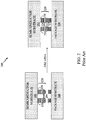
- Conventional solutions for preventing the undercut 126 to the copper layer 122 of the copper pillars 120 include changing the etch process to reduce an amount of,the undercut 126. Changing the etch process, however, involves a fundamental process change to develop a new etch mechanism. Another conventional solution is increasing a bump diameter of the copper pillars 120, for example, as shown in FIGURE 2 .
- FIGURE 2 illustrates a chip attach process 200 for attaching a semiconductor substrate (e.g., an IC die/chip, flip chip) 202 (e.g., an IC device) to a package substrate 260 or another semiconductor substrate.
- a semiconductor substrate e.g., an IC die/chip, flip chip
- FIGURE 2 shows the semiconductor substrate 202 facing downwardly, whereas the semiconductor substrate 102 of FIGURE 1 is oriented to face upwardly.
- a bump diameter of the solder bumps 224 as well as the copper layer 222 of the copper pillars 220 is increased. This increase in the bump diameter, however, is limited by a bump pitch 204.
- a solder bridge 226 develops after the thermal process to couple the solder bumps 224 of the copper pillars 220 to contact pads 262 of the package substrate 260 during flip chip assembly. That is, flip chip reflow to couple the contact pads 262 and the solder bumps 224 of the copper pillars 220 results in the solder bridge 226 between the solder bumps 224.
- US 2011/266667 A1 discloses a method of fabricating a conductive interconnect on a semiconductor substrate comprising: depositing a conductive seed layer on the semiconductor substrate, depositing and patterning a photoresist material on the conductive seed layer, fabricating a conductive material (a conductive pillar) on regions of the conductive seed layer exposed by the patterned photoresist material, stripping the photoresist material, depositing an organic dielectric material on the conductive seed layer and the conductive material, patterning the organic spin on dielectric material to form an organic collar that surrounds the conductive material and etching the conductive seed layer to form a conductive support layer, thereby forming the conductive interconnect comprising the conductive support layer, the conductive material and the organic collar.
- JP 2011 091 087 A discloses a method of fabricating a conductive interconnect on a semiconductor substrate comprising: depositing a conductive seed layer on the semiconductor substrate, depositing and patterning a photoresist material on the conductive seed layer, fabricating a conductive material on regions of the conductive seed layer exposed by the patterned photoresist material, stripping the photoresist material, depositing an organic spin on dielectric material on the conductive seed layer and the conductive material, patterning the organic spin on dielectric material to form an organic collar that partially surrounds the conductive material, curing the organic collar by heating and etching the conductive seed layer to form a conductive support layer, thereby forming the conductive interconnect comprising the conductive support layer, the conductive material and the organic collar.
- US 2007/231957 A1 discloses a method of fabricating a conductive interconnect on a semiconductor substrate comprising: depositing a conductive seed layer on the semiconductor substrate, depositing and patterning a photoresist material on the conductive seed layer, fabricating a conductive material on regions of the conductive seed layer exposed by the patterned photoresist material, stripping the photoresist material, depositing an inorganic dielectric material on the conductive seed layer and the conductive material by a CVD method, patterning the inorganic dielectric material to form an inorganic collar that surrounds the conductive material and etching the conductive seed layer to form a conductive support layer, thereby forming the conductive interconnect comprising the conductive support layer, the conductive material and the inorganic collar.
- JP S64 2339 A discloses a method in which an organic insulating film having an aperture is provided on an intermediate metal layer on an electrode pad and a metal-plated layer is provided in the aperture of the organic insulating film to form a bump, followed by etching the intermediate metal layer and softening the organic insulating film to cover the sidewalls of the etched intermediate metal layer.
- EP 1 239 332 B1 discloses a silazane precursor material which is transformed to inorganic SiO 2 by heating. See also "Spin-on dielectrics" http://web.archive.org/web/20121014003631/http://www.azem.com/en/Products/Silicon -technology/Spin-on%20Dielectrics.aspx.
- IC integrated circuit
- MEMS micro-electromechanical systems
- Conventional solutions for preventing the undercut 126 to the copper layer 122 include changing the etch process to reduce an amount of the undercut 126. Changing the etch process, however, involves a fundamental process change to develop a new etch mechanism.
- Another conventional solution is increasing a bump diameter of the copper pillars, for example, as shown in FIGURE 2 . Increasing the bump diameter, however, is limited by a bump pitch 204. When the clearance (e.g., the bump pitch 204) between solder bumps 224 is reduced by the increased bump diameter, a solder bridge 226 develops after the thermal process to couple the solder bumps 224 of the copper pillars 220 to contact pads 262 of the package substrate 260 during flip chip assembly.
- FIGURE 3 is a block diagram illustrating a plating method 300 for fabricating conductive interconnects 340 including an inorganic collar 350, according to one aspect of the present disclosure.
- the conventional process of FIGURE 1 may be used to form conductive material stacks 320 on a conductive seed layer 304 deposited on a semiconductor substrate (wafer or die) 302.
- the conductive material stacks 320 are used to form conductive interconnects following stripping of the photoresist.
- the conductive material stacks 320 may be formed using an electroplating process to grow a first conductive layer 322 and a second conductive layer 324, for example, arranged as a conductive pillar.
- the first conductive layer 322 may include, but is not limited to, copper (Cu), nickel (Ni), gold (Au), or other like plated metal that will not melt during thermal treatment (e.g., reflow).
- the second conductive layer 324 may include, but is not limited to, indium (In), bismuth (Bi), and lead (Pb), or other like plated metal or alloy that will melt during thermal treatment (e.g., reflow).
- a barrier layer (not shown) may be deposited between the first conductive layer 322 and the second conductive layer 324.
- a thickness of the first conductive layer 322 may be in the range of a few to hundreds of microns.
- a thickness of the second conductive layer 324 may be in the range of a few to hundreds of microns.
- an organic spin on dielectric material 306 may be applied on the conductive seed layer 304 and the conductive material stacks 320.
- the organic spin on dielectric material 306 is a photosensitive spin on dielectric material that transitions from an organic material to an inorganic material following a thermal process.
- An example material is a photosensitive spin on dielectric (PSOD) from AZ Electronic Materials.
- the organic spin on dielectric material 306 is patterned using, for example, a photolithographic process to form an organic collar 310.
- a thickness of the organic collar 310 may be in the range of a few hundred nanometers to a few micrometers (microns).
- the conductive seed layer 304 is etched to form a conductive support layer 330. This process may be performed using a non-isotropic etch that removes the conductive seed layer 304 in all directions because excessive remaining portions of the conductive seed layer 304 may cause faulty interconnect operation.
- the organic collar 310 protects the first conductive layer 322 of the conductive material stacks 320 and the conductive support layer 330 from the over etching shown in FIGURE 1 .
- a thermal process is performed to reflow the second conductive layer 324 of the conductive material stacks 320 to form conductive interconnects 340. Surface tension causes the round shape of the second conductive layer 324.
- FIGURES 5 and 6 An alternative embodiment is shown in FIGURES 5 and 6 , in which a single conductive material 520/620 replaces the conductive material stacks 320.
- the thermal process causes a transition of the spin on dielectric material 306 of the organic collar 310 from an organic material to an inorganic material that may be similar in composition to, for example, silicon dioxide (SiO 2 ).
- the inorganic material forms an inorganic collar 350 that partially surrounds the conductive interconnects 340.
- the inorganic collar 350 is composed of a curable inorganic material, including silicon, that exhibits a thermal cross link reaction during the thermal process.
- the thermal process for forming the inorganic collar 350 causes the spin on dielectric material 306 to flow onto the sidewalls of the conductive support layer 330 prior to curing into the inorganic collar 350.
- a thermal crosslink reaction during the thermal treatment causes the spin on dielectric material 306 of the organic collar 310 to flow onto the conductive seed layer 304.
- a thermal cross link reaction is a chemical reaction that joins the smaller molecules of the spin on dielectric material 306 into a large network that forms a cured, solid matter of the inorganic collar 350. That is, the thermal treatment causes the spin on dielectric material 306 to flow onto the sidewalls of the conductive support layer 330
- the inorganic collar 350 has good thermal conductivity.
- the semiconductor substrate 302, including the conductive interconnects 340, may be assembled into an integrated circuit (IC) device package.
- the inorganic collar 350 provides an improved heat dissipation path when compared to the other organic materials around the conductive interconnects 340, such as underfill and/or molding compound of the assembled package.
- heat is easily dissipated through the inorganic collar 350 of the conductive interconnects 340.
- the inorganic collar 350 can withstand high temperatures.
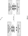
- FIGURE 4 is a block diagram illustrating an assembly process 400 for attaching a semiconductor substrate (e.g., an IC device, such as a flip chip device or a MEMS device) 402 to a package substrate 460 using conductive interconnects 440 according to one aspect of the present disclosure.
- the semiconductor substrate 402 includes conductive interconnects 440 formed by the process shown in FIGURE 3 and separated by a distance (e.g., an interconnect pitch 406).
- the conductive interconnects 440 include a conductive material stack of a first conductive layer 422 and a second conductive layer 424 formed on a conductive support layer 430 and surrounded by an inorganic collar 450. Following reflow, the second conductive layer 424 of the conductive interconnects 440 couples to contact pads 462 of the package substrate 460.
- the use of the inorganic collar 450 protects the composition of the first conductive layer 422 of the conductive interconnects 440 during the seed layer etch to eliminate or reduce any undercutting to the first conductive layer 422.
- Protecting the composition of the first conductive layer 422 may increase an extremely low-K (ELK) robustness and improve a interconnect fatigue life of the conductive interconnects 440.
- the inorganic collar 450 prevents the solder bridge problem shown in FIGURE 2 . Eliminating the solder bridge problem enables a further reduction of the interconnect pitch 406 to support fine pitch/size designs for devices such as micro-electromechanical systems (MEMS) devices as well as flip chip devices.
- MEMS micro-electromechanical systems
- eliminating undercutting maintains a diameter of the first conductive layer 422 of the conductive interconnects 440 to provide an increased contact area of the conductive interconnects 440 to the semiconductor substrate 402.
- the increased contact area may improve the connectivity as well as the integrity of the conductive interconnects 440.
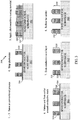
- FIGURE 5 is a block diagram illustrating a plating method 500 for fabricating a conductive interconnect 540 including an inorganic collar 550 according to another aspect of the present disclosure.
- An example of a conductive interconnect 540 is supported by a semiconductor substrate 502.
- the conductive interconnect 540 includes an inorganic collar 550 that surrounds a single conductive material 520 and sidewalls of a conductive support layer 530.
- the conventional process of FIGURE 1 may be used to form a photoresist pattern 508.
- a single conductive material 520 is electroplated within the photoresist pattern 508 and on a conductive seed layer 504 deposited on a semiconductor substrate (wafer or die) 502.
- the photoresist pattern 508 is stripped to expose the single conductive material 520 and the conductive seed layer 504.
- Steps 5 to 7 are similar to steps 5 to 7 in FIGURE 3 , however, the single conductive material 520 is provided in place of the conductive material stacks 320.
- the conductive interconnects 540 include the single conductive material 520, which does not reflow during the thermal process to form the inorganic collar 550.
- a thermal process causes the spin on dielectric material 506 to flow onto sidewalls of the conductive support layer 530 prior to curing into the inorganic collar 550 to complete formation of the conductive interconnects 540, as shown in step 8.
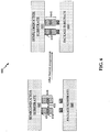
- FIGURE 6 is a block diagram illustrating an assembly process 600 for attaching a semiconductor substrate (e.g., an IC device, such as a flip chip device or a MEMS device) 602 to a package substrate 660 using conductive interconnects 640 according to one aspect of the present disclosure.
- the semiconductor substrate 602 includes conductive interconnects 640 formed by the process shown in FIGURE 5 and separated by a distance (e.g., an interconnect pitch 606).
- the conductive interconnects 640 include a single conductive material 620 formed on a conductive support layer 630 and surrounded by an inorganic collar 650.
- the single conductive material 620 of the conductive interconnects 640 can be directly bonded to the conductive pads 662 using thermal compression bonding or other like processes for applying a sufficient amount of heat and pressure to couple with the conductive pads 662. Following the thermal compression bonding, the single conductive material 620 of the conductive interconnects 640 couples to the conductive pads 662 to join the semiconductor substrate 602 to the package substrate 660.
- FIGURE 7 is a block diagram illustrating a method 700 for fabricating a conductive interconnect including an inorganic collar according to one aspect of the present disclosure.
- a conductive material is fabricated on a conductive seed layer.
- conductive material stacks 320 are formed on a conductive seed layer 304 deposited on a semiconductor substrate 302.
- the conductive material stacks 320 are used to form conductive interconnects following stripping of a photoresist.
- the conductive material stacks 320 may by formed using an electroplating process to grow a first conductive layer 322 (e.g., copper (Cu), nickel (Ni), gold (Au)) and a second conductive layer 324 (e.g., indium (In), bismuth (Bi), and lead (Pb)).
- a single conductive material 520 is fabricated on a conductive seed layer 504 deposited on a semiconductor substrate 502, as shown in FIGURE 5 .
- an organic collar is formed to partially surround the conductive material.
- an organic spin on dielectric material 306 may be applied on the conductive seed layer 304 and the conductive material stacks 320.
- the organic spin on dielectric material 306 is patterned using, for example, a photolithographic process to form the organic collar 310.
- an organic spin on dielectric material 506 is applied on a conductive seed layer 504 and the single conductive material 520.
- a photolithographic process forms the organic collar 510 around the single conductive material 520, as shown in FIGURE 5 .
- the conductive seed layer is etched to form a conductive support layer.
- the conductive seed layer 304 is etched to form a conductive support layer 330.
- the conductive seed layer 504 is etched to form a conductive support layer 530.
- the conductive interconnect is subjected to a thermal process (i.e., heated) to transition the organic collar into an inorganic collar that partially surrounds the conductive material.
- the inorganic collar is disposed on sidewalls of a conductive support layer.
- the inorganic collar 350 is composed of a curable inorganic material that exhibits a thermal cross link reaction during the thermal process.
- the thermal process for forming the inorganic collar 350 causes the spin on dielectric material 306 to flow onto sidewalls of the conductive support layer 330 prior to curing into the inorganic collar 350.
- the method 700 of FIGURE 7 may be carried out by the structures and components described above in relation to FIGURES 3 and 4 .
- a spin on dielectric material 506 is applied to the conductive seed layer 504 and a single conductive material 520.
- the organic spin on dielectric material 506 is patterned using, for example, a photolithographic process to form the organic collar 510.
- the conductive seed layer 504 is then etched to form a conductive support layer 530.
- a thermal process causes the spin on dielectric material 506 to flow onto sidewalls of the conductive support layer 530 prior to curing into the inorganic collar 550, as shown in FIGURE 5 .
- This alternative method may be carried out by the structures and components described in relation to FIGURES 5 and 6 .
- etch loss to a conductive material during a seed layer etch process is a concern for the conductive material(s) during the conductive interconnect formation process, for example, as shown in FIGURES 3 to 7 .
- the method 700 may protect the first conductive material 522 of the conductive material stacks 320 or a single conductive material 520 during the seed layer etch process.
- an organic spin on dielectric material 306/506 e.g., a photosensitive spin on dielectric material is coated on the conductive material stacks 320 or the single conductive material 520.
- This dielectric material 306/506 is patterned using a photolithographic process to form an organic material having a collar structure (e.g., the organic collar 310/510) around the conductive material stacks 320 or the single conductive material 520.
- the organic collar 310/510 can protect the conductive material stacks 320 or the single conductive material 520 from over etching.
- a thermal process reflows the second conductive layer 324 of the conductive material stacks 320 to form the conductive interconnects 340 including the inorganic collar 350.
- the conductive interconnects 540 include the single conductive material 520, which does not reflow during the thermal process to form the inorganic collar 550.
- a thermal process causes a transition of the spin on dielectric material 306/506 from an organic material to an inorganic material, such as silicon dioxide (SiO 2 ).
- the thermal process causes the spin on dielectric material 306/506 to flow onto the sidewalls of the conductive support layer 330/530 to form the inorganic collar 350/550.
- the inorganic collar 350 around the conductive material stacks 320 also prevents the solder bridge problem during semiconductor chip assembly. Eliminating the solder bridge problem enables a further reduction of the interconnect pitch to support fine pitch/size designs for semiconductor devices.
- eliminating undercutting maintains a diameter of the first conductive layer 422 or the single conductive material 520 of the conductive interconnects 440/540.
- This configuration provides an increased contact area of the conductive interconnects 440/540 to the semiconductor substrate 402/502. The increased contact areas also improve the connectivity as well as the integrity of the conductive interconnects 440/540.
- a conductive interconnect in one configuration, includes a conductive material on a conductive support layer.
- the conductive interconnect also includes means for protecting the conductive material and the conductive support layer of the conductive interconnect.
- the protecting means may partially surround the conductive material and is disposed on sidewalls of the conductive support layer.
- the protecting means may be the inorganic collar 350/450/550/650 configured to perform the functions recited by the protecting means.
- the aforementioned means may be any component or any structure configured to perform the functions recited by the aforementioned means.
- FIGURE 8 shows an exemplary wireless communication system 800 in which a configuration of the disclosed conductive interconnect including the inorganic collar may be advantageously employed.
- FIGURE 8 shows three remote units 820, 830, and 850 and two base stations 840. It will be recognized that wireless communication systems may have many more remote units and base stations.
- Remote units 820, 830, and 850 include conductive interconnects 825A, 825B, and 825C, respectively.
- FIGURE 8 shows forward link signals 880 from the base stations 840 and the remote units 820, 830, and 850 and reverse link signals 890 from the remote units 820, 830, and 850 to base stations 840.
- the remote unit 820 is shown as a mobile telephone
- remote unit 830 is shown as a portable computer
- remote unit 850 is shown as a fixed location remote unit in a wireless local loop system.
- the remote units may be cell phones, hand-held personal communication systems (PCS) units, a set top box, a music player, a video player, an entertainment unit, a navigation device, portable data units, such as personal data assistants, or fixed location data units such as meter reading equipment.
- FIGURE 8 illustrates remote units, which may employ conductive interconnects according to the teachings of the disclosure, the disclosure is not limited to these exemplary illustrated units.
- the conductive interconnects according to configurations of the present disclosure may be suitably employed in any device.
- the methodologies described herein may be implemented by various components depending upon the application. For example, these methodologies may be implemented in hardware, firmware, software, or any combination thereof
- the processing units may be implemented within one or more application specific integrated circuits (ASICs), digital signal processors (DSPs), digital signal processing devices (DSPDs), programmable logic devices (PLDs), field programmable gate arrays (FPGAs), processors, controllers, micro-controllers, microprocessors, electronic devices, other electronic units designed to perform the functions described herein, or a combination thereof.
- ASICs application specific integrated circuits
- DSPs digital signal processors
- DSPDs digital signal processing devices
- PLDs programmable logic devices
- FPGAs field programmable gate arrays
- processors controllers, micro-controllers, microprocessors, electronic devices, other electronic units designed to perform the functions described herein, or a combination thereof.
- the methodologies may be implemented with modules (e.g., procedures, functions, and so on) that perform the functions described herein.
- Any machine-readable medium tangibly embodying instructions may be used in implementing the methodologies described herein.
- software codes may be stored in a memory and executed by a processor unit.
- Memory may be implemented within the processor unit or external to the processor unit.
- memory refers to any type of long term, short term, volatile, nonvolatile, or other memory and is not to be limited to any particular type of memory or number of memories, or type of media upon which memory is stored.
- the functions may be stored as one or more instructions or code on a computer-readable medium. Examples include computer-readable media encoded with a data structure and computer-readable media encoded with a computer program. Computer-readable media includes physical computer storage media. A storage medium may be any available medium that can be accessed by a computer.
- such computer-readable media can comprise RAM, ROM, EEPROM, CD-ROM or other optical disk storage, magnetic disk storage or other magnetic storage devices, or any other medium that can be used to store desired program code in the form of instructions or data structures and that can be accessed by a computer; disk and disc, as used herein, includes compact disc (CD), laser disc, optical disc, digital versatile disc (DVD), floppy disk and blu-ray disc where disks usually reproduce data magnetically, while discs reproduce data optically with lasers. Combinations of the above should also be included within the scope of computer-readable media.
- instructions and/or data may be provided as signals on transmission media included in a communication apparatus.
- a communication apparatus may include a transceiver having signals indicative of instructions and data. The instructions and data are configured to cause one or more processors to implement the functions outlined in the claims.
Landscapes
- Engineering & Computer Science (AREA)
- Microelectronics & Electronic Packaging (AREA)
- Manufacturing & Machinery (AREA)
- Computer Hardware Design (AREA)
- Power Engineering (AREA)
- Physics & Mathematics (AREA)
- Condensed Matter Physics & Semiconductors (AREA)
- General Physics & Mathematics (AREA)
- Internal Circuitry In Semiconductor Integrated Circuit Devices (AREA)
- Wire Bonding (AREA)
- Micromachines (AREA)
Applications Claiming Priority (3)
| Application Number | Priority Date | Filing Date | Title |
|---|---|---|---|
| US201261721889P | 2012-11-02 | 2012-11-02 | |
| US13/764,261 US20140124877A1 (en) | 2012-11-02 | 2013-02-11 | Conductive interconnect including an inorganic collar |
| PCT/US2013/067568 WO2014070926A1 (en) | 2012-11-02 | 2013-10-30 | A conductive interconnect including an inorganic collar |
Publications (2)
| Publication Number | Publication Date |
|---|---|
| EP2915191A1 EP2915191A1 (en) | 2015-09-09 |
| EP2915191B1 true EP2915191B1 (en) | 2020-04-15 |
Family
ID=50621573
Family Applications (1)
| Application Number | Title | Priority Date | Filing Date |
|---|---|---|---|
| EP13795327.9A Active EP2915191B1 (en) | 2012-11-02 | 2013-10-30 | Method of fabricating a conductive interconnect with an inorganic collar |
Country Status (6)
Families Citing this family (6)
| Publication number | Priority date | Publication date | Assignee | Title |
|---|---|---|---|---|
| TWI568662B (zh) * | 2013-03-08 | 2017-02-01 | 先技股份有限公司 | 微機電裝置 |
| US9698116B2 (en) * | 2014-10-31 | 2017-07-04 | Nxp Usa, Inc. | Thick-silver layer interface for a semiconductor die and corresponding thermal layer |
| US9713264B2 (en) | 2014-12-18 | 2017-07-18 | Intel Corporation | Zero-misalignment via-pad structures |
| US10475736B2 (en) | 2017-09-28 | 2019-11-12 | Intel Corporation | Via architecture for increased density interface |
| US20210159198A1 (en) * | 2019-11-24 | 2021-05-27 | Nanya Technology Corporation | Semiconductor structure and manufacturing method thereof |
| CN114649287A (zh) * | 2022-05-19 | 2022-06-21 | 甬矽半导体(宁波)有限公司 | 一种芯片制作方法、芯片连接方法以及芯片 |
Family Cites Families (15)
| Publication number | Priority date | Publication date | Assignee | Title |
|---|---|---|---|---|
| JPS642339A (en) * | 1987-06-24 | 1989-01-06 | Nec Corp | Manufacture of semiconductor device |
| US5445894A (en) * | 1991-04-22 | 1995-08-29 | Dow Corning Corporation | Ceramic coatings |
| JPH10209163A (ja) * | 1997-01-21 | 1998-08-07 | Citizen Watch Co Ltd | 半導体装置およびその製造方法 |
| JP3654485B2 (ja) * | 1997-12-26 | 2005-06-02 | 富士通株式会社 | 半導体装置の製造方法 |
| KR100804444B1 (ko) * | 2000-08-31 | 2008-02-20 | 에이제토 엘렉토로닉 마티리알즈 가부시키가이샤 | 패턴화된 폴리실라잔 막의 형성방법 및 감광성 폴리실라잔도막의 소성방법 |
| US6734568B2 (en) * | 2001-08-29 | 2004-05-11 | Kabushiki Kaisha Toshiba | Semiconductor device and method of manufacturing the same |
| US20050274871A1 (en) * | 2004-06-10 | 2005-12-15 | Jin Li | Method and apparatus for collecting photons in a solid state imaging sensor |
| US20070238222A1 (en) * | 2006-03-28 | 2007-10-11 | Harries Richard J | Apparatuses and methods to enhance passivation and ILD reliability |
| JP4768491B2 (ja) * | 2006-03-30 | 2011-09-07 | Okiセミコンダクタ株式会社 | 半導体装置の製造方法 |
| JP4247690B2 (ja) * | 2006-06-15 | 2009-04-02 | ソニー株式会社 | 電子部品及その製造方法 |
| US9524945B2 (en) * | 2010-05-18 | 2016-12-20 | Taiwan Semiconductor Manufacturing Company, Ltd. | Cu pillar bump with L-shaped non-metal sidewall protection structure |
| JP2011091087A (ja) * | 2009-10-20 | 2011-05-06 | Fujitsu Ltd | 半導体装置とその製造方法 |
| US8441124B2 (en) * | 2010-04-29 | 2013-05-14 | Taiwan Semiconductor Manufacturing Company, Ltd. | Cu pillar bump with non-metal sidewall protection structure |
| US9018758B2 (en) * | 2010-06-02 | 2015-04-28 | Taiwan Semiconductor Manufacturing Company, Ltd. | Cu pillar bump with non-metal sidewall spacer and metal top cap |
| JP5663607B2 (ja) * | 2011-02-10 | 2015-02-04 | パナソニックIpマネジメント株式会社 | 半導体装置 |
-
2013
- 2013-02-11 US US13/764,261 patent/US20140124877A1/en not_active Abandoned
- 2013-10-30 EP EP13795327.9A patent/EP2915191B1/en active Active
- 2013-10-30 JP JP2015540752A patent/JP2016500930A/ja active Pending
- 2013-10-30 WO PCT/US2013/067568 patent/WO2014070926A1/en active Application Filing
- 2013-10-30 CN CN201380057472.4A patent/CN104769711B/zh active Active
- 2013-10-30 KR KR1020157014345A patent/KR20150082395A/ko not_active Withdrawn
Non-Patent Citations (1)
| Title |
|---|
| None * |
Also Published As
| Publication number | Publication date |
|---|---|
| KR20150082395A (ko) | 2015-07-15 |
| JP2016500930A (ja) | 2016-01-14 |
| EP2915191A1 (en) | 2015-09-09 |
| US20140124877A1 (en) | 2014-05-08 |
| CN104769711A (zh) | 2015-07-08 |
| CN104769711B (zh) | 2018-06-01 |
| WO2014070926A1 (en) | 2014-05-08 |
Similar Documents
| Publication | Publication Date | Title |
|---|---|---|
| EP2915191B1 (en) | Method of fabricating a conductive interconnect with an inorganic collar | |
| US7476564B2 (en) | Flip-chip packaging process using copper pillar as bump structure | |
| KR101764021B1 (ko) | 반도체 구조체 및 그 제조 방법 | |
| KR102007780B1 (ko) | 멀티 범프 구조의 전기적 연결부를 포함하는 반도체 소자의 제조방법 | |
| KR101910198B1 (ko) | 반도체 장치, 반도체 장치의 제조 방법 및 배선 기판의 제조 방법 | |
| CN106711104B (zh) | 封装基板及其制作工艺、半导体元件封装结构及制作工艺 | |
| US10163817B2 (en) | Semiconductor device structure comprising a plurality of metal oxide fibers and method for forming the same | |
| US11101231B2 (en) | Semiconductor package and method of manufacturing the same | |
| KR101605600B1 (ko) | 반도체 디바이스의 제조 방법 및 이에 따른 반도체 디바이스 | |
| US8759971B2 (en) | Semiconductor apparatus | |
| EP3361497A1 (en) | Semiconductor package with embedded supporter and method for fabricating the same | |
| KR20150091932A (ko) | 반도체 디바이스의 제조 방법 및 이에 따른 반도체 디바이스 | |
| US8445321B2 (en) | Semiconductor device and method of manufacturing the same | |
| US9159685B2 (en) | Conductive structure and method for forming the same | |
| US8624241B2 (en) | Semiconductor chip, stack-type semiconductor package | |
| KR101926713B1 (ko) | 반도체 패키지 및 그 제조방법 | |
| CN109564897B (zh) | 镍-锡微凸块结构及其制造方法 | |
| US7067350B1 (en) | Method of manufacturing a semiconductor device using electrical contacts formed in an isolation layer | |
| US20190096836A1 (en) | Bump structure, semiconductor package including the bump structure, and method of forming the bump structure | |
| JP2016181555A (ja) | バンプ構造とバンプ接合構造およびバンプ製造方法 | |
| JP2010157544A (ja) | 半導体装置及びその製造方法、並びに電子機器 | |
| TW201432870A (zh) | 包含無機套環之導電互連 | |
| KR102157877B1 (ko) | 반도체 패키지 | |
| KR100790683B1 (ko) | 플립칩 패키지 및 그 제조방법 | |
| TW202510242A (zh) | 倒裝晶片凸塊金屬層及凸塊結構 |
Legal Events
| Date | Code | Title | Description |
|---|---|---|---|
| PUAI | Public reference made under article 153(3) epc to a published international application that has entered the european phase |
Free format text: ORIGINAL CODE: 0009012 |
|
| 17P | Request for examination filed |
Effective date: 20150501 |
|
| AK | Designated contracting states |
Kind code of ref document: A1 Designated state(s): AL AT BE BG CH CY CZ DE DK EE ES FI FR GB GR HR HU IE IS IT LI LT LU LV MC MK MT NL NO PL PT RO RS SE SI SK SM TR |
|
| AX | Request for extension of the european patent |
Extension state: BA ME |
|
| DAX | Request for extension of the european patent (deleted) | ||
| STAA | Information on the status of an ep patent application or granted ep patent |
Free format text: STATUS: EXAMINATION IS IN PROGRESS |
|
| 17Q | First examination report despatched |
Effective date: 20190318 |
|
| REG | Reference to a national code |
Ref country code: DE Ref legal event code: R079 Ref document number: 602013067984 Country of ref document: DE Free format text: PREVIOUS MAIN CLASS: H01L0023485000 Ipc: H01L0021600000 |
|
| RIC1 | Information provided on ipc code assigned before grant |
Ipc: H01L 21/60 20060101AFI20190913BHEP Ipc: H01L 23/485 20060101ALI20190913BHEP |
|
| GRAP | Despatch of communication of intention to grant a patent |
Free format text: ORIGINAL CODE: EPIDOSNIGR1 |
|
| STAA | Information on the status of an ep patent application or granted ep patent |
Free format text: STATUS: GRANT OF PATENT IS INTENDED |
|
| INTG | Intention to grant announced |
Effective date: 20191106 |
|
| RIN1 | Information on inventor provided before grant (corrected) |
Inventor name: HAN, MICHAEL Inventor name: SUN, YANGYANG Inventor name: ZHAO, LILY |
|
| GRAS | Grant fee paid |
Free format text: ORIGINAL CODE: EPIDOSNIGR3 |
|
| GRAA | (expected) grant |
Free format text: ORIGINAL CODE: 0009210 |
|
| STAA | Information on the status of an ep patent application or granted ep patent |
Free format text: STATUS: THE PATENT HAS BEEN GRANTED |
|
| AK | Designated contracting states |
Kind code of ref document: B1 Designated state(s): AL AT BE BG CH CY CZ DE DK EE ES FI FR GB GR HR HU IE IS IT LI LT LU LV MC MK MT NL NO PL PT RO RS SE SI SK SM TR |
|
| REG | Reference to a national code |
Ref country code: CH Ref legal event code: EP |
|
| REG | Reference to a national code |
Ref country code: DE Ref legal event code: R096 Ref document number: 602013067984 Country of ref document: DE |
|
| REG | Reference to a national code |
Ref country code: IE Ref legal event code: FG4D |
|
| REG | Reference to a national code |
Ref country code: AT Ref legal event code: REF Ref document number: 1258280 Country of ref document: AT Kind code of ref document: T Effective date: 20200515 |
|
| REG | Reference to a national code |
Ref country code: NL Ref legal event code: MP Effective date: 20200415 |
|
| REG | Reference to a national code |
Ref country code: LT Ref legal event code: MG4D |
|
| PG25 | Lapsed in a contracting state [announced via postgrant information from national office to epo] |
Ref country code: SE Free format text: LAPSE BECAUSE OF FAILURE TO SUBMIT A TRANSLATION OF THE DESCRIPTION OR TO PAY THE FEE WITHIN THE PRESCRIBED TIME-LIMIT Effective date: 20200415 Ref country code: FI Free format text: LAPSE BECAUSE OF FAILURE TO SUBMIT A TRANSLATION OF THE DESCRIPTION OR TO PAY THE FEE WITHIN THE PRESCRIBED TIME-LIMIT Effective date: 20200415 Ref country code: IS Free format text: LAPSE BECAUSE OF FAILURE TO SUBMIT A TRANSLATION OF THE DESCRIPTION OR TO PAY THE FEE WITHIN THE PRESCRIBED TIME-LIMIT Effective date: 20200815 Ref country code: NO Free format text: LAPSE BECAUSE OF FAILURE TO SUBMIT A TRANSLATION OF THE DESCRIPTION OR TO PAY THE FEE WITHIN THE PRESCRIBED TIME-LIMIT Effective date: 20200715 Ref country code: GR Free format text: LAPSE BECAUSE OF FAILURE TO SUBMIT A TRANSLATION OF THE DESCRIPTION OR TO PAY THE FEE WITHIN THE PRESCRIBED TIME-LIMIT Effective date: 20200716 Ref country code: PT Free format text: LAPSE BECAUSE OF FAILURE TO SUBMIT A TRANSLATION OF THE DESCRIPTION OR TO PAY THE FEE WITHIN THE PRESCRIBED TIME-LIMIT Effective date: 20200817 Ref country code: NL Free format text: LAPSE BECAUSE OF FAILURE TO SUBMIT A TRANSLATION OF THE DESCRIPTION OR TO PAY THE FEE WITHIN THE PRESCRIBED TIME-LIMIT Effective date: 20200415 Ref country code: LT Free format text: LAPSE BECAUSE OF FAILURE TO SUBMIT A TRANSLATION OF THE DESCRIPTION OR TO PAY THE FEE WITHIN THE PRESCRIBED TIME-LIMIT Effective date: 20200415 |
|
| REG | Reference to a national code |
Ref country code: AT Ref legal event code: MK05 Ref document number: 1258280 Country of ref document: AT Kind code of ref document: T Effective date: 20200415 |
|
| PG25 | Lapsed in a contracting state [announced via postgrant information from national office to epo] |
Ref country code: LV Free format text: LAPSE BECAUSE OF FAILURE TO SUBMIT A TRANSLATION OF THE DESCRIPTION OR TO PAY THE FEE WITHIN THE PRESCRIBED TIME-LIMIT Effective date: 20200415 Ref country code: RS Free format text: LAPSE BECAUSE OF FAILURE TO SUBMIT A TRANSLATION OF THE DESCRIPTION OR TO PAY THE FEE WITHIN THE PRESCRIBED TIME-LIMIT Effective date: 20200415 Ref country code: BG Free format text: LAPSE BECAUSE OF FAILURE TO SUBMIT A TRANSLATION OF THE DESCRIPTION OR TO PAY THE FEE WITHIN THE PRESCRIBED TIME-LIMIT Effective date: 20200715 Ref country code: HR Free format text: LAPSE BECAUSE OF FAILURE TO SUBMIT A TRANSLATION OF THE DESCRIPTION OR TO PAY THE FEE WITHIN THE PRESCRIBED TIME-LIMIT Effective date: 20200415 |
|
| PG25 | Lapsed in a contracting state [announced via postgrant information from national office to epo] |
Ref country code: AL Free format text: LAPSE BECAUSE OF FAILURE TO SUBMIT A TRANSLATION OF THE DESCRIPTION OR TO PAY THE FEE WITHIN THE PRESCRIBED TIME-LIMIT Effective date: 20200415 |
|
| REG | Reference to a national code |
Ref country code: DE Ref legal event code: R097 Ref document number: 602013067984 Country of ref document: DE |
|
| PG25 | Lapsed in a contracting state [announced via postgrant information from national office to epo] |
Ref country code: RO Free format text: LAPSE BECAUSE OF FAILURE TO SUBMIT A TRANSLATION OF THE DESCRIPTION OR TO PAY THE FEE WITHIN THE PRESCRIBED TIME-LIMIT Effective date: 20200415 Ref country code: IT Free format text: LAPSE BECAUSE OF FAILURE TO SUBMIT A TRANSLATION OF THE DESCRIPTION OR TO PAY THE FEE WITHIN THE PRESCRIBED TIME-LIMIT Effective date: 20200415 Ref country code: CZ Free format text: LAPSE BECAUSE OF FAILURE TO SUBMIT A TRANSLATION OF THE DESCRIPTION OR TO PAY THE FEE WITHIN THE PRESCRIBED TIME-LIMIT Effective date: 20200415 Ref country code: EE Free format text: LAPSE BECAUSE OF FAILURE TO SUBMIT A TRANSLATION OF THE DESCRIPTION OR TO PAY THE FEE WITHIN THE PRESCRIBED TIME-LIMIT Effective date: 20200415 Ref country code: SM Free format text: LAPSE BECAUSE OF FAILURE TO SUBMIT A TRANSLATION OF THE DESCRIPTION OR TO PAY THE FEE WITHIN THE PRESCRIBED TIME-LIMIT Effective date: 20200415 Ref country code: DK Free format text: LAPSE BECAUSE OF FAILURE TO SUBMIT A TRANSLATION OF THE DESCRIPTION OR TO PAY THE FEE WITHIN THE PRESCRIBED TIME-LIMIT Effective date: 20200415 Ref country code: AT Free format text: LAPSE BECAUSE OF FAILURE TO SUBMIT A TRANSLATION OF THE DESCRIPTION OR TO PAY THE FEE WITHIN THE PRESCRIBED TIME-LIMIT Effective date: 20200415 Ref country code: ES Free format text: LAPSE BECAUSE OF FAILURE TO SUBMIT A TRANSLATION OF THE DESCRIPTION OR TO PAY THE FEE WITHIN THE PRESCRIBED TIME-LIMIT Effective date: 20200415 |
|
| PLBE | No opposition filed within time limit |
Free format text: ORIGINAL CODE: 0009261 |
|
| STAA | Information on the status of an ep patent application or granted ep patent |
Free format text: STATUS: NO OPPOSITION FILED WITHIN TIME LIMIT |
|
| PG25 | Lapsed in a contracting state [announced via postgrant information from national office to epo] |
Ref country code: SK Free format text: LAPSE BECAUSE OF FAILURE TO SUBMIT A TRANSLATION OF THE DESCRIPTION OR TO PAY THE FEE WITHIN THE PRESCRIBED TIME-LIMIT Effective date: 20200415 Ref country code: PL Free format text: LAPSE BECAUSE OF FAILURE TO SUBMIT A TRANSLATION OF THE DESCRIPTION OR TO PAY THE FEE WITHIN THE PRESCRIBED TIME-LIMIT Effective date: 20200415 |
|
| 26N | No opposition filed |
Effective date: 20210118 |
|
| PG25 | Lapsed in a contracting state [announced via postgrant information from national office to epo] |
Ref country code: SI Free format text: LAPSE BECAUSE OF FAILURE TO SUBMIT A TRANSLATION OF THE DESCRIPTION OR TO PAY THE FEE WITHIN THE PRESCRIBED TIME-LIMIT Effective date: 20200415 |
|
| REG | Reference to a national code |
Ref country code: CH Ref legal event code: PL |
|
| PG25 | Lapsed in a contracting state [announced via postgrant information from national office to epo] |
Ref country code: LU Free format text: LAPSE BECAUSE OF NON-PAYMENT OF DUE FEES Effective date: 20201030 Ref country code: MC Free format text: LAPSE BECAUSE OF FAILURE TO SUBMIT A TRANSLATION OF THE DESCRIPTION OR TO PAY THE FEE WITHIN THE PRESCRIBED TIME-LIMIT Effective date: 20200415 |
|
| REG | Reference to a national code |
Ref country code: BE Ref legal event code: MM Effective date: 20201031 |
|
| PG25 | Lapsed in a contracting state [announced via postgrant information from national office to epo] |
Ref country code: BE Free format text: LAPSE BECAUSE OF NON-PAYMENT OF DUE FEES Effective date: 20201031 Ref country code: CH Free format text: LAPSE BECAUSE OF NON-PAYMENT OF DUE FEES Effective date: 20201031 Ref country code: LI Free format text: LAPSE BECAUSE OF NON-PAYMENT OF DUE FEES Effective date: 20201031 |
|
| PG25 | Lapsed in a contracting state [announced via postgrant information from national office to epo] |
Ref country code: IE Free format text: LAPSE BECAUSE OF NON-PAYMENT OF DUE FEES Effective date: 20201030 |
|
| PG25 | Lapsed in a contracting state [announced via postgrant information from national office to epo] |
Ref country code: TR Free format text: LAPSE BECAUSE OF FAILURE TO SUBMIT A TRANSLATION OF THE DESCRIPTION OR TO PAY THE FEE WITHIN THE PRESCRIBED TIME-LIMIT Effective date: 20200415 Ref country code: MT Free format text: LAPSE BECAUSE OF FAILURE TO SUBMIT A TRANSLATION OF THE DESCRIPTION OR TO PAY THE FEE WITHIN THE PRESCRIBED TIME-LIMIT Effective date: 20200415 Ref country code: CY Free format text: LAPSE BECAUSE OF FAILURE TO SUBMIT A TRANSLATION OF THE DESCRIPTION OR TO PAY THE FEE WITHIN THE PRESCRIBED TIME-LIMIT Effective date: 20200415 |
|
| PG25 | Lapsed in a contracting state [announced via postgrant information from national office to epo] |
Ref country code: MK Free format text: LAPSE BECAUSE OF FAILURE TO SUBMIT A TRANSLATION OF THE DESCRIPTION OR TO PAY THE FEE WITHIN THE PRESCRIBED TIME-LIMIT Effective date: 20200415 |
|
| PGFP | Annual fee paid to national office [announced via postgrant information from national office to epo] |
Ref country code: GB Payment date: 20220914 Year of fee payment: 10 |
|
| PGFP | Annual fee paid to national office [announced via postgrant information from national office to epo] |
Ref country code: FR Payment date: 20220916 Year of fee payment: 10 |
|
| PGFP | Annual fee paid to national office [announced via postgrant information from national office to epo] |
Ref country code: DE Payment date: 20220914 Year of fee payment: 10 |
|
| REG | Reference to a national code |
Ref country code: DE Ref legal event code: R119 Ref document number: 602013067984 Country of ref document: DE |
|
| GBPC | Gb: european patent ceased through non-payment of renewal fee |
Effective date: 20231030 |
|
| PG25 | Lapsed in a contracting state [announced via postgrant information from national office to epo] |
Ref country code: GB Free format text: LAPSE BECAUSE OF NON-PAYMENT OF DUE FEES Effective date: 20231030 |
|
| PG25 | Lapsed in a contracting state [announced via postgrant information from national office to epo] |
Ref country code: GB Free format text: LAPSE BECAUSE OF NON-PAYMENT OF DUE FEES Effective date: 20231030 Ref country code: FR Free format text: LAPSE BECAUSE OF NON-PAYMENT OF DUE FEES Effective date: 20231031 Ref country code: DE Free format text: LAPSE BECAUSE OF NON-PAYMENT OF DUE FEES Effective date: 20240501 |