EP2910095B1 - Heat sink attachment apparatus and method - Google Patents
Heat sink attachment apparatus and method Download PDFInfo
- Publication number
- EP2910095B1 EP2910095B1 EP13786360.1A EP13786360A EP2910095B1 EP 2910095 B1 EP2910095 B1 EP 2910095B1 EP 13786360 A EP13786360 A EP 13786360A EP 2910095 B1 EP2910095 B1 EP 2910095B1
- Authority
- EP
- European Patent Office
- Prior art keywords
- electronic device
- shield
- circuit board
- heat sink
- bend
- Prior art date
- Legal status (The legal status is an assumption and is not a legal conclusion. Google has not performed a legal analysis and makes no representation as to the accuracy of the status listed.)
- Active
Links
Images


Classifications
-
- H—ELECTRICITY
- H05—ELECTRIC TECHNIQUES NOT OTHERWISE PROVIDED FOR
- H05K—PRINTED CIRCUITS; CASINGS OR CONSTRUCTIONAL DETAILS OF ELECTRIC APPARATUS; MANUFACTURE OF ASSEMBLAGES OF ELECTRICAL COMPONENTS
- H05K7/00—Constructional details common to different types of electric apparatus
- H05K7/20—Modifications to facilitate cooling, ventilating, or heating
- H05K7/2039—Modifications to facilitate cooling, ventilating, or heating characterised by the heat transfer by conduction from the heat generating element to a dissipating body
- H05K7/20409—Outer radiating structures on heat dissipating housings, e.g. fins integrated with the housing
-
- G—PHYSICS
- G06—COMPUTING OR CALCULATING; COUNTING
- G06F—ELECTRIC DIGITAL DATA PROCESSING
- G06F1/00—Details not covered by groups G06F3/00 - G06F13/00 and G06F21/00
- G06F1/16—Constructional details or arrangements
- G06F1/20—Cooling means
-
- G—PHYSICS
- G06—COMPUTING OR CALCULATING; COUNTING
- G06F—ELECTRIC DIGITAL DATA PROCESSING
- G06F1/00—Details not covered by groups G06F3/00 - G06F13/00 and G06F21/00
- G06F1/16—Constructional details or arrangements
- G06F1/18—Packaging or power distribution
- G06F1/181—Enclosures
-
- G—PHYSICS
- G06—COMPUTING OR CALCULATING; COUNTING
- G06F—ELECTRIC DIGITAL DATA PROCESSING
- G06F1/00—Details not covered by groups G06F3/00 - G06F13/00 and G06F21/00
- G06F1/16—Constructional details or arrangements
- G06F1/18—Packaging or power distribution
- G06F1/183—Internal mounting support structures, e.g. for printed circuit boards, internal connecting means
-
- H—ELECTRICITY
- H01—ELECTRIC ELEMENTS
- H01L—SEMICONDUCTOR DEVICES NOT COVERED BY CLASS H10
- H01L23/00—Details of semiconductor or other solid state devices
- H01L23/34—Arrangements for cooling, heating, ventilating or temperature compensation ; Temperature sensing arrangements
- H01L23/40—Mountings or securing means for detachable cooling or heating arrangements ; fixed by friction, plugs or springs
- H01L23/4093—Snap-on arrangements, e.g. clips
-
- H—ELECTRICITY
- H05—ELECTRIC TECHNIQUES NOT OTHERWISE PROVIDED FOR
- H05K—PRINTED CIRCUITS; CASINGS OR CONSTRUCTIONAL DETAILS OF ELECTRIC APPARATUS; MANUFACTURE OF ASSEMBLAGES OF ELECTRICAL COMPONENTS
- H05K7/00—Constructional details common to different types of electric apparatus
- H05K7/02—Arrangements of circuit components or wiring on supporting structure
- H05K7/12—Resilient or clamping means for holding component to structure
-
- H—ELECTRICITY
- H05—ELECTRIC TECHNIQUES NOT OTHERWISE PROVIDED FOR
- H05K—PRINTED CIRCUITS; CASINGS OR CONSTRUCTIONAL DETAILS OF ELECTRIC APPARATUS; MANUFACTURE OF ASSEMBLAGES OF ELECTRICAL COMPONENTS
- H05K7/00—Constructional details common to different types of electric apparatus
- H05K7/20—Modifications to facilitate cooling, ventilating, or heating
- H05K7/2039—Modifications to facilitate cooling, ventilating, or heating characterised by the heat transfer by conduction from the heat generating element to a dissipating body
- H05K7/20436—Inner thermal coupling elements in heat dissipating housings, e.g. protrusions or depressions integrally formed in the housing
- H05K7/2049—Pressing means used to urge contact, e.g. springs
-
- H—ELECTRICITY
- H05—ELECTRIC TECHNIQUES NOT OTHERWISE PROVIDED FOR
- H05K—PRINTED CIRCUITS; CASINGS OR CONSTRUCTIONAL DETAILS OF ELECTRIC APPARATUS; MANUFACTURE OF ASSEMBLAGES OF ELECTRICAL COMPONENTS
- H05K9/00—Screening of apparatus or components against electric or magnetic fields
-
- H—ELECTRICITY
- H05—ELECTRIC TECHNIQUES NOT OTHERWISE PROVIDED FOR
- H05K—PRINTED CIRCUITS; CASINGS OR CONSTRUCTIONAL DETAILS OF ELECTRIC APPARATUS; MANUFACTURE OF ASSEMBLAGES OF ELECTRICAL COMPONENTS
- H05K9/00—Screening of apparatus or components against electric or magnetic fields
- H05K9/0007—Casings
- H05K9/002—Casings with localised screening
- H05K9/0022—Casings with localised screening of components mounted on printed circuit boards [PCB]
- H05K9/0024—Shield cases mounted on a PCB, e.g. cans or caps or conformal shields
- H05K9/0032—Shield cases mounted on a PCB, e.g. cans or caps or conformal shields having multiple parts, e.g. frames mating with lids
-
- H—ELECTRICITY
- H01—ELECTRIC ELEMENTS
- H01L—SEMICONDUCTOR DEVICES NOT COVERED BY CLASS H10
- H01L23/00—Details of semiconductor or other solid state devices
- H01L23/34—Arrangements for cooling, heating, ventilating or temperature compensation ; Temperature sensing arrangements
- H01L23/36—Selection of materials, or shaping, to facilitate cooling or heating, e.g. heatsinks
- H01L23/367—Cooling facilitated by shape of device
- H01L23/3672—Foil-like cooling fins or heat sinks
-
- H—ELECTRICITY
- H01—ELECTRIC ELEMENTS
- H01L—SEMICONDUCTOR DEVICES NOT COVERED BY CLASS H10
- H01L2924/00—Indexing scheme for arrangements or methods for connecting or disconnecting semiconductor or solid-state bodies as covered by H01L24/00
- H01L2924/0001—Technical content checked by a classifier
- H01L2924/0002—Not covered by any one of groups H01L24/00, H01L24/00 and H01L2224/00
-
- Y—GENERAL TAGGING OF NEW TECHNOLOGICAL DEVELOPMENTS; GENERAL TAGGING OF CROSS-SECTIONAL TECHNOLOGIES SPANNING OVER SEVERAL SECTIONS OF THE IPC; TECHNICAL SUBJECTS COVERED BY FORMER USPC CROSS-REFERENCE ART COLLECTIONS [XRACs] AND DIGESTS
- Y10—TECHNICAL SUBJECTS COVERED BY FORMER USPC
- Y10T—TECHNICAL SUBJECTS COVERED BY FORMER US CLASSIFICATION
- Y10T29/00—Metal working
- Y10T29/49—Method of mechanical manufacture
- Y10T29/49002—Electrical device making
- Y10T29/49227—Insulator making
Definitions
- the present principles relate generally to electronic devices and, more particularly, to a heat sink attachment apparatus and method for an electronic device.
- Consumer/market preference for set top boxes and the like is to have such devices be small/compact.
- set top boxes and the like must be density packed with internal components, which causes space to be at a premium and makes heat generation a significant problem.
- An electronic device according to claim 1 is proposed. Moreover an electronic device according to independent claim 9 is proposed.
- an electronic device includes a circuit board having heat generating components thereon.
- the electronic device further includes spring clips or bend tabs.
- the electronic device also includes a heat sink, disposed over the circuit board, through which heat from the circuit board and the components thereon is released or dissipated.
- the heat sink has a generally flat horizontal base and a series of vertically directed fins.
- the heat sink is secured to at least one of the circuit board and at least one of the components thereon by the spring clips or bend tabs being positioned at a periphery of the horizontal base.
- the spring clips or bend tabs have distal contact prongs that contact and apply downward force on the horizontal base.
- the electronic device further comprises a shield attached to at least one of a bottom surface of the circuit board and a bottom frame of the electronic device, the shield being further attached to the spring clips or the bend tabs.
- an electronic device includes a cover, side walls perpendicular to the cover, a bottom frame parallel to the cover, and a circuit board having heat generating components thereon.
- the electronic device further includes spring clips or bend tabs.
- the electronic device also includes a heat sink, disposed over the circuit board, through which heat from the circuit board and the components thereon is released or dissipated.
- the heat sink has a generally flat horizontal base and a series of vertically directed fins. The heat sink is secured to at least one of the circuit board and at least one of the components thereon by the spring clips or bend tabs which are positioned at a periphery of the horizontal base.
- the spring clips or bend tabs have distal contact prongs that contact and apply downward force on the horizontal base.
- the electronic device further comprises a shield attached to at least one of a bottom surface of the circuit board and a bottom frame of the electronic device in which the shield can be attached to the spring clips or bend tabs.
- the shield can be substantially permanently attached to at least one of the bottom surface of the circuit board and the bottom frame of the electronic device or the shield can be removably attached to at least one of the bottom surface of the circuit board and the bottom frame of the electronic device.
- the shield can comprise wrap-around bend tabs for attaching the shield to at least one of the bottom surface of the circuit board and the bottom frame of the electronic device.
- the heat sink can comprise a series of grooves inter-dispersed between the series of fins on a top side of the horizontal base, and the distal contact prongs can contact and apply downward force onto one or more of the grooves.
- the present principles are directed to a heat sink attachment apparatus and method for an electronic device.
- the present principles are applicable to any electronic device including, but not limited to, a set top box, computer, game console, DVD player, CD player or the like, where the electronic device is provided with an improved heat dissipation system. More specifically, a heat sink is provided over a heat generating component or a circuit board having heat generating components thereon, in which spring clip or bend tab assemblies are provided that may be individual pieces or a part of a shield that prevent the heat sink from coming loosing or rattling. Further, the spring clip or bend tab assemblies enhance the thermal contact between the heat sink and thermal contact pads or heat generating components which can be on a circuit board.
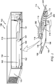
- FIG. 1 shows a perspective view 199 of an electronic device 100 with some elements thereof shown outside of the electronic device 100, in accordance with an embodiment of the present principles.
- the electronic device 100 can be, for example, but is not limited to, a set top box, a hard drive, a DVD player, and so forth.
- the electronic device 100 includes a cover 150, side walls 151, a bottom frame 152, a printed circuit board (PCB) 101 with heat generating components thereon, a heat sink 115, a heat sink attachment apparatus (also interchangeably referred to here as "spring clip or bend tab assembly") 114, and an element 118 which can be a thermal pad and/or an integrated circuit chip 118.
- the thermal pad 118 can be on the PCB 101 and/or on the bottom surface 195 of the heat sink 115.
- the thermal pad 118 can be attached to the PCB 101 or to the bottom surface 195 of the heat sink 115, to facilitate heat extraction.
- the heat sink 115 or a contact pad (not shown) under the heat sink 115 can contact the chip 118 on the PCB 101.
- the integrated circuit chip can be on the PCB 101 and the thermal pad can be on the integrated circuit chip, where the heat sink 115 is then placed on the thermal pad.
- the PCB 101 has a bottom surface 191 and a top surface 192.
- the heat sink has a bottom surface 195 and a top surface 196 (see FIG. 4 ).
- the side walls 151 are perpendicular to the cover 150.
- the bottom frame 152 is parallel to the cover 150.
- a front panel of the electronic device 100 is removed to show the PCB 101.
- the heat sink 115 can have a generally flat horizontal base 281 and a series of vertically directed fins or columns (hereinafter "fins") 282. Each of the fins 282 can extend substantially from edge to opposing edge of the PCB 101. The fins 282 can have a series of grooves 283 which can assist in maximizing surface area, thereby increasing emissivity. In a particular embodiment, the heat sink 115 can cover less than 50% of the top view surface area of the PCB 101. In another embodiment, the heat sink 115 can cover less than 25% of the top view surface area of the PCB 101. Of course, other percentages can also be used in accordance with the teachings of the present principles.
- the spring clip or bend tab assembly 114 includes spring clips or bend tabs 119.
- the spring clip or bend tab assembly 114 can be, for example, bolted, soldered, clipped, riveted and/or screwed to the shield 116.
- the heat sink 115 is attached to the electronic device 100 (or element thereof) using the spring clips or bend tabs 119.
- the spring clips or bend tabs 119 can be individual pieces or a part of a shield 116 that has a bottom surface 193 and a top surface 194 and sidewalls 241 on a periphery 188 of the shield 116.
- the sidewalls 241 can substantially follow the periphery 166 of the PCB 101.
- the sidewalls 241 can be vertical and integrated with the spring clip or bend tabs 119.
- the spring clips or bend tabs 119 can be positioned at a periphery 176 of the flat horizontal base 281 of the heat sink 115. When engaged, the spring clips or bend tabs 119 hold the heat sink 115 in place and prevent the heat sink 115 from coming loose, thus providing a low cost way to secure the heat sink 115.
- heat sink mounting holes on the PCB 101 worsen the trace layout utilization of compact and high density electrical design. For example, avoiding the use of a 3mm mounting hole on a PCB can easily yield an extra 12 traces to be laid out in the PCB space vacated by the hole on a single layer. For multi-layer PCBs, the increase in trace runs is even greater.
- the present principles are applicable to systems which may need shielding (from, for example, radio frequency (RF) emissions) and heat sinking.
- the idea of merging the shield with the heat sink holders saves money and space.
- the spring clips or bend tabs 119 can be formed from a unitary single piece of metal along with the shield 116, or the spring clips or bend tabs 119 can be welded or snapped onto the shield walls 241.
- the spring clips or bend tabs 119 can be substantially permanently attached to the shield 116, e.g., by collectively being made from a unitary single piece of metal, being soldered together, being welded together, being riveted together, and so forth.
- the spring clips or bend tabs can be removably attached to the shield, e.g., using screws, bolts, clips, springs, and so forth.
- FIG. 2 shows a perspective see-through view 299 of the heat sink 115 and spring clip or bend tab assembly 114 with the spring clips or bend tabs 119 not engaged, in accordance with an embodiment of the present principles.
- the spring clips or bend tabs 119 (shown encircled for the sake of clarity) are not engaged, but when the distal contact prongs 119D of the spring clips or bend tabs 119 are twisted or rotated or bent inward they will contact the heat sink 115 at contact points 221 and hold the heat sink 115 down.
- the contact points 221 can be one or more of the grooves 283 and/or any portion of the top surface 196 of the heat sink 115.
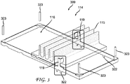
- FIG. 3 shows another perspective see-through view 399 of the heat sink 115 and spring clip or bend tab assembly 114 with the spring clips or bend tabs 119 engaged, in accordance with an embodiment of the present principles.
- the heat sink 115 is shown as being raised so that the spring clips or bend tabs 119 (shown encircled for the sake of clarity) can be clearly viewed.
- the spring clips or bend tabs 119 are engaged by being bent (or twisted or rotated or distorted) to contact the heat sink 115.
- distal contact prongs 119D of the spring clips or bend tabs 119 are bent inward to contact the heat sink 115.
- the distal contact prongs 119D trap the heat sink 115 in place and maintain a certain amount of pressure on the heat sink 115 and, e.g., a chip (or other element) there under.
- the distal contact prongs 119D of the spring clips or bend tabs 119 can be positioned between adjacent fins of the heat sink 115.
- Shield tabs 322 can extend downward from the shield walls 241 and these tabs 322 can bend inward to wrap around components such as the bottom surface 195 (see FIG. 4 ) of the heat sink 115 or the bottom surface 191 of the PCB 101 or an interior frame within the electronic device 100.
- the shield tabs 322 can help secure the shield 116 to the electronic device 100.
- bolts, screws, and/or rivets 323 can be used to attached the shield 116 to the PCB 101 and/or a frame of the electronic device 100, e.g., through complementary holes in the shield 116.
- FIG. 4 shows a perspective view 499 of another spring clip or bend tab assembly 414, in accordance with an embodiment of the present principles.
- the spring clip or bend tab assembly 414 clips the heat sink down by using paperclip-like spring clips or bend tabs 419.
- the spring clips or bend tabs 419 can be bent inward and directed downward to contact and hold the heat sink 115 in place.
- the spring clips or bend tabs 419 can be separate from the shield 116 and can be welded or soldered to the shield 416 or PCB 101 or frame (e.g., bottom frame 152).
- the heat sink 115 is located on a thermal contact pad 118 that is located on the top surface 192 of the PCB 101 (not shown in FIG. 4 ) and/or on the bottom surface 195 of the heat sink 115.
- the spring clips or bend tabs 419 can be located on the outside of the shield 116, and the heat sink 115 can snap in from the top.
- FIG. 5 shows a perspective view 599 of another spring clip or bend tab assembly 514, in accordance with an embodiment of the present principles
- FIG. 6 shows another perspective view 699 of yet another spring clip or bend tab assembly 614, in accordance with an embodiment of the present principles
- the spring clip or bend tab assembly 514 includes spring clips or bend tabs 519.
- the spring clip or bend tab assembly 614 includes spring clips or bend tabs 619.
- the spring clips or bend tabs 519 each include a respective prong 519D that is attached from three sides and bends from a top portion of the spring clips or bend tabs 519 towards the heat sink 115 to engage the contact points 221 on the heat sink 115.
- the spring clips or bend tabs 619 each include a respective prong that attached from one side and bends from the corresponding side of the spring clips or bend tabs 619 towards the heat sink 115 to engage the contact points 221 on the heat sink 115.
- the spring clip or bend tab assembly 514 and/or the spring clip or bend tab assembly 614 can be separate from the shield 516 and they can also be welded or soldered to the shield 116 to hold the heat sink 115 down.
- a portion of the spring clips or bend tabs can contact the heat sink 115 on an upper surface in between the fins or rails 282 and/or on a surface outside of the fins or rails 282.
- FIG. 7 shows a flowchart for a method 700 for providing a heat sink attachment apparatus, in accordance with an embodiment of the present principles.
- step 705 provide a single piece of sheet metal.
- step 710 form vertical sidewalls on the sheet metal to surround a periphery of a horizontal circuit board.
- step 715 provide tabs that protrude upward from the vertical sidewalls or upward from the circuit board adjacent the vertical sidewalls.
- Step 715 can involve forming the tabs on the single piece of sheet metal or attaching the tabs to the shield.
- step 720 position the formed sheet metal so that the vertical sidewalls surround the periphery of the circuit board.
- step 725 attach the formed sheet metal to the circuit board or a frame component under the circuit board.
- step 730 place a heat sink over the circuit board, the heat sink for extracting heat from the circuit board and components thereon.
- bend, twist, rotate or distort the tabs to contact an upper surface of the heat sink, thereby applying a downward force on the heat sink to cause the heat sink to contact at least one of the circuit board and the components thereon.
Landscapes
- Engineering & Computer Science (AREA)
- Microelectronics & Electronic Packaging (AREA)
- Physics & Mathematics (AREA)
- Theoretical Computer Science (AREA)
- General Physics & Mathematics (AREA)
- Power Engineering (AREA)
- Computer Hardware Design (AREA)
- Thermal Sciences (AREA)
- General Engineering & Computer Science (AREA)
- Human Computer Interaction (AREA)
- Condensed Matter Physics & Semiconductors (AREA)
- Cooling Or The Like Of Electrical Apparatus (AREA)
- Cooling Or The Like Of Semiconductors Or Solid State Devices (AREA)
- Chemical & Material Sciences (AREA)
- Materials Engineering (AREA)
Applications Claiming Priority (2)
| Application Number | Priority Date | Filing Date | Title |
|---|---|---|---|
| US201261715876P | 2012-10-19 | 2012-10-19 | |
| PCT/US2013/065529 WO2014062974A1 (en) | 2012-10-19 | 2013-10-17 | Heat sink attachment apparatus and method |
Publications (2)
| Publication Number | Publication Date |
|---|---|
| EP2910095A1 EP2910095A1 (en) | 2015-08-26 |
| EP2910095B1 true EP2910095B1 (en) | 2019-08-14 |
Family
ID=49519112
Family Applications (1)
| Application Number | Title | Priority Date | Filing Date |
|---|---|---|---|
| EP13786360.1A Active EP2910095B1 (en) | 2012-10-19 | 2013-10-17 | Heat sink attachment apparatus and method |
Country Status (7)
Families Citing this family (12)
| Publication number | Priority date | Publication date | Assignee | Title |
|---|---|---|---|---|
| WO2016048298A1 (en) * | 2014-09-24 | 2016-03-31 | Hewlett Packard Enterprise Development Lp | Heat sink with a load spreading bar |
| US10356948B2 (en) | 2015-12-31 | 2019-07-16 | DISH Technologies L.L.C. | Self-adjustable heat spreader system for set-top box assemblies |
| US10624245B2 (en) * | 2016-06-23 | 2020-04-14 | Laird Technologies, Inc. | Laser weldable brackets for attachment of heat sinks to board level shields |
| US9893474B1 (en) * | 2016-10-12 | 2018-02-13 | International Business Machines Corporation | Active cable heat sink |
| CN106507651B (zh) * | 2016-12-30 | 2019-11-29 | 韩端科技(深圳)有限公司 | 电子设备 |
| US10785864B2 (en) * | 2017-09-21 | 2020-09-22 | Amazon Technologies, Inc. | Printed circuit board with heat sink |
| USD837753S1 (en) | 2018-06-27 | 2019-01-08 | Advanced Thermal Solutions, Inc. | Heat sink clip |
| USD877098S1 (en) | 2018-06-27 | 2020-03-03 | Advanced Thermal Solutions, Inc. | Heat sink clip and attachment |
| USD876372S1 (en) | 2018-06-27 | 2020-02-25 | Advanced Thermal Solutions, Inc. | Heat sink clip and attachment |
| USD835590S1 (en) | 2018-06-27 | 2018-12-11 | Advanced Thermal Solutions, Inc. | Heat sink clip |
| US11971739B2 (en) * | 2019-01-10 | 2024-04-30 | Makersan Makina Otomotiv Sanayi Ticaret Anonim Sirketi | Joystick with precise control |
| US11778728B2 (en) * | 2020-10-28 | 2023-10-03 | Arris Enterprises Llc | Pass-through latching heat sink |
Family Cites Families (25)
| Publication number | Priority date | Publication date | Assignee | Title |
|---|---|---|---|---|
| US5304735A (en) * | 1992-02-14 | 1994-04-19 | Aavid Engineering, Inc. | Heat sink for an electronic pin grid array |
| US5436798A (en) * | 1994-01-21 | 1995-07-25 | Wakefield Engineering, Inc. | Spring clip and heat sink assembly for electronic components |
| US5411199A (en) * | 1994-03-07 | 1995-05-02 | Motorola, Inc. | Method for attaching a shield |
| SE9401203L (sv) * | 1994-04-11 | 1995-10-12 | Ellemtel Utvecklings Ab | Skärm och kylare |
| US5621244A (en) * | 1994-05-16 | 1997-04-15 | Lin; Shih-Jen | Fin assembly for an integrated circuit |
| GB2295927A (en) * | 1994-12-08 | 1996-06-12 | Gareth Rhys Baron | Mounting of an integrated circuit on a printed circuit board |
| US5570271A (en) * | 1995-03-03 | 1996-10-29 | Aavid Engineering, Inc. | Heat sink assemblies |
| US5576933A (en) | 1995-05-15 | 1996-11-19 | Wakefield Engineering, Inc. | Clamping heat sink for an electric device |
| US5881800A (en) * | 1998-04-03 | 1999-03-16 | Chung; Kuang-Hua | Heat sink fastener |
| CN2342343Y (zh) * | 1998-08-04 | 1999-10-06 | 钟光华 | 散热器固定座结构 |
| US6617685B1 (en) * | 1999-08-30 | 2003-09-09 | Sun Microsystems, Inc. | Clip heat sink assembly |
| EP1128432B1 (de) | 2000-02-24 | 2016-04-06 | Infineon Technologies AG | Befestigung von Halbleitermodulen an einem Kühlkörper |
| US7061774B2 (en) | 2000-12-18 | 2006-06-13 | Franklin Zhigang Zhang | Computer board with dual shield housing and heat sink expansion zone apparatuses |
| US6856511B1 (en) * | 2003-07-17 | 2005-02-15 | Cisco Technology, Inc. | Methods and apparatus for attaching a heat sink to a circuit board component |
| US8902603B2 (en) | 2004-02-06 | 2014-12-02 | Carmen Rapisarda | Solder and lead free electronic circuit and method of manufacturing same |
| JP2006222388A (ja) * | 2005-02-14 | 2006-08-24 | Toshiba Corp | 電子機器の放熱装置及び放熱方法 |
| CN1953646A (zh) * | 2005-10-18 | 2007-04-25 | 鸿富锦精密工业(深圳)有限公司 | 能防电磁干扰的散热装置 |
| US7355857B2 (en) * | 2006-02-07 | 2008-04-08 | Methode Electronics, Inc. | Heat sink gasket |
| WO2008070873A2 (en) * | 2006-12-07 | 2008-06-12 | Finisar Corporation | Electromagnetic radiation containment and heat management in an electronic module |
| CN101601131A (zh) * | 2007-02-15 | 2009-12-09 | 日本电气株式会社 | 用于安装半导体封装的结构 |
| US7567439B2 (en) | 2007-08-10 | 2009-07-28 | Fu Zhun Precision Industry (Shen Zhen) Co., Ltd. | Heat dissipation device having a rotatable fastener |
| CN101754639A (zh) * | 2008-12-02 | 2010-06-23 | 台达电子工业股份有限公司 | 散热器固定结构 |
| CN201726632U (zh) * | 2010-04-15 | 2011-01-26 | 鸿富锦精密工业(深圳)有限公司 | 电子产品之散热片固定结构 |
| US20140036451A1 (en) * | 2012-07-31 | 2014-02-06 | Glenn C. Simon | Heat sink assembly |
| US9146062B2 (en) * | 2013-03-01 | 2015-09-29 | Radian Thermal Products, Inc. | Interlocking clip heatsink mounting system |
-
2013
- 2013-10-17 US US14/435,049 patent/US9603286B2/en active Active
- 2013-10-17 KR KR1020157010075A patent/KR20150073992A/ko not_active Withdrawn
- 2013-10-17 CN CN201380054313.9A patent/CN105009699A/zh active Pending
- 2013-10-17 WO PCT/US2013/065529 patent/WO2014062974A1/en active Application Filing
- 2013-10-17 BR BR112015008465-6A patent/BR112015008465B1/pt active IP Right Grant
- 2013-10-17 EP EP13786360.1A patent/EP2910095B1/en active Active
- 2013-10-17 JP JP2015537844A patent/JP2015537377A/ja not_active Withdrawn
Non-Patent Citations (1)
| Title |
|---|
| None * |
Also Published As
| Publication number | Publication date |
|---|---|
| WO2014062974A1 (en) | 2014-04-24 |
| US20150282388A1 (en) | 2015-10-01 |
| KR20150073992A (ko) | 2015-07-01 |
| US9603286B2 (en) | 2017-03-21 |
| BR112015008465B1 (pt) | 2021-07-20 |
| CN105009699A (zh) | 2015-10-28 |
| BR112015008465A2 (pt) | 2017-07-04 |
| EP2910095A1 (en) | 2015-08-26 |
| JP2015537377A (ja) | 2015-12-24 |
Similar Documents
| Publication | Publication Date | Title |
|---|---|---|
| EP2910095B1 (en) | Heat sink attachment apparatus and method | |
| JP4703454B2 (ja) | 光モジュール用ケージ実装構造 | |
| EP3495917A1 (en) | Printed circuit assembly with vents and electronic device with the assembly | |
| CN201336790Y (zh) | 散热装置 | |
| EP2540148B1 (en) | Miniature multilayer radiative cooling case with hidden quick release snaps | |
| US10568207B2 (en) | Printed circuit board assembly and assembling method thereof | |
| US20140153192A1 (en) | Module cage with integrated emi aspect | |
| US6937475B2 (en) | Mounting and grounding assembly for circuit board mounted parallel to chassis bottom | |
| US6046906A (en) | Vent chimney heat sink design for an electrical assembly | |
| EP3050411B1 (en) | Fixation of heat sink on sfp/xfp cage | |
| US7821785B1 (en) | Heatsinks and a spring in a baffle slot between adjacent components | |
| US9743556B1 (en) | Electrical connector structure | |
| US11659689B2 (en) | Heatsink assembly for an electronic device | |
| US6101093A (en) | Wrap around clip for an electronic cartridge | |
| JP5717619B2 (ja) | 電子機器ユニット | |
| US20110235259A1 (en) | Expansion card assembly and heat shielding cover for expansion card thereof | |
| WO2023028765A1 (en) | Apparatus for providing thermal management and electromagnetic interference shielding | |
| EP2910096B1 (en) | Electronic device with combination heat sink/blower or fan assembly | |
| CN202748699U (zh) | 防尘件以及包括此防尘件的主板 | |
| WO2013095490A1 (en) | Heat sink base and shield | |
| CN202197485U (zh) | 散热模块及其基座 | |
| US20100246131A1 (en) | Heat sink and motherboard assembly utilizing the heat sink | |
| CN103089686A (zh) | 风扇模块 | |
| KR20140081273A (ko) | 반도체 소자의 히트싱크 |
Legal Events
| Date | Code | Title | Description |
|---|---|---|---|
| PUAI | Public reference made under article 153(3) epc to a published international application that has entered the european phase |
Free format text: ORIGINAL CODE: 0009012 |
|
| 17P | Request for examination filed |
Effective date: 20150410 |
|
| AK | Designated contracting states |
Kind code of ref document: A1 Designated state(s): AL AT BE BG CH CY CZ DE DK EE ES FI FR GB GR HR HU IE IS IT LI LT LU LV MC MK MT NL NO PL PT RO RS SE SI SK SM TR |
|
| AX | Request for extension of the european patent |
Extension state: BA ME |
|
| RAP1 | Party data changed (applicant data changed or rights of an application transferred) |
Owner name: THOMSON LICENSING |
|
| DAX | Request for extension of the european patent (deleted) | ||
| REG | Reference to a national code |
Ref country code: DE Ref legal event code: R079 Ref document number: 602013059202 Country of ref document: DE Free format text: PREVIOUS MAIN CLASS: H05K0007200000 Ipc: H01L0023367000 |
|
| RIC1 | Information provided on ipc code assigned before grant |
Ipc: H05K 7/20 20060101ALI20190118BHEP Ipc: H01L 23/40 20060101ALI20190118BHEP Ipc: H05K 7/12 20060101ALI20190118BHEP Ipc: H01L 23/367 20060101AFI20190118BHEP Ipc: H05K 9/00 20060101ALI20190118BHEP |
|
| RAP1 | Party data changed (applicant data changed or rights of an application transferred) |
Owner name: INTERDIGITAL CE PATENT HOLDINGS |
|
| GRAP | Despatch of communication of intention to grant a patent |
Free format text: ORIGINAL CODE: EPIDOSNIGR1 |
|
| STAA | Information on the status of an ep patent application or granted ep patent |
Free format text: STATUS: GRANT OF PATENT IS INTENDED |
|
| INTG | Intention to grant announced |
Effective date: 20190319 |
|
| GRAS | Grant fee paid |
Free format text: ORIGINAL CODE: EPIDOSNIGR3 |
|
| GRAA | (expected) grant |
Free format text: ORIGINAL CODE: 0009210 |
|
| STAA | Information on the status of an ep patent application or granted ep patent |
Free format text: STATUS: THE PATENT HAS BEEN GRANTED |
|
| AK | Designated contracting states |
Kind code of ref document: B1 Designated state(s): AL AT BE BG CH CY CZ DE DK EE ES FI FR GB GR HR HU IE IS IT LI LT LU LV MC MK MT NL NO PL PT RO RS SE SI SK SM TR |
|
| REG | Reference to a national code |
Ref country code: GB Ref legal event code: FG4D |
|
| REG | Reference to a national code |
Ref country code: CH Ref legal event code: EP Ref country code: AT Ref legal event code: REF Ref document number: 1168034 Country of ref document: AT Kind code of ref document: T Effective date: 20190815 |
|
| REG | Reference to a national code |
Ref country code: IE Ref legal event code: FG4D |
|
| REG | Reference to a national code |
Ref country code: DE Ref legal event code: R096 Ref document number: 602013059202 Country of ref document: DE |
|
| REG | Reference to a national code |
Ref country code: NL Ref legal event code: FP |
|
| REG | Reference to a national code |
Ref country code: LT Ref legal event code: MG4D |
|
| PG25 | Lapsed in a contracting state [announced via postgrant information from national office to epo] |
Ref country code: PT Free format text: LAPSE BECAUSE OF FAILURE TO SUBMIT A TRANSLATION OF THE DESCRIPTION OR TO PAY THE FEE WITHIN THE PRESCRIBED TIME-LIMIT Effective date: 20191216 Ref country code: BG Free format text: LAPSE BECAUSE OF FAILURE TO SUBMIT A TRANSLATION OF THE DESCRIPTION OR TO PAY THE FEE WITHIN THE PRESCRIBED TIME-LIMIT Effective date: 20191114 Ref country code: LT Free format text: LAPSE BECAUSE OF FAILURE TO SUBMIT A TRANSLATION OF THE DESCRIPTION OR TO PAY THE FEE WITHIN THE PRESCRIBED TIME-LIMIT Effective date: 20190814 Ref country code: HR Free format text: LAPSE BECAUSE OF FAILURE TO SUBMIT A TRANSLATION OF THE DESCRIPTION OR TO PAY THE FEE WITHIN THE PRESCRIBED TIME-LIMIT Effective date: 20190814 Ref country code: SE Free format text: LAPSE BECAUSE OF FAILURE TO SUBMIT A TRANSLATION OF THE DESCRIPTION OR TO PAY THE FEE WITHIN THE PRESCRIBED TIME-LIMIT Effective date: 20190814 Ref country code: FI Free format text: LAPSE BECAUSE OF FAILURE TO SUBMIT A TRANSLATION OF THE DESCRIPTION OR TO PAY THE FEE WITHIN THE PRESCRIBED TIME-LIMIT Effective date: 20190814 Ref country code: NO Free format text: LAPSE BECAUSE OF FAILURE TO SUBMIT A TRANSLATION OF THE DESCRIPTION OR TO PAY THE FEE WITHIN THE PRESCRIBED TIME-LIMIT Effective date: 20191114 |
|
| REG | Reference to a national code |
Ref country code: AT Ref legal event code: MK05 Ref document number: 1168034 Country of ref document: AT Kind code of ref document: T Effective date: 20190814 |
|
| PG25 | Lapsed in a contracting state [announced via postgrant information from national office to epo] |
Ref country code: ES Free format text: LAPSE BECAUSE OF FAILURE TO SUBMIT A TRANSLATION OF THE DESCRIPTION OR TO PAY THE FEE WITHIN THE PRESCRIBED TIME-LIMIT Effective date: 20190814 Ref country code: RS Free format text: LAPSE BECAUSE OF FAILURE TO SUBMIT A TRANSLATION OF THE DESCRIPTION OR TO PAY THE FEE WITHIN THE PRESCRIBED TIME-LIMIT Effective date: 20190814 Ref country code: IS Free format text: LAPSE BECAUSE OF FAILURE TO SUBMIT A TRANSLATION OF THE DESCRIPTION OR TO PAY THE FEE WITHIN THE PRESCRIBED TIME-LIMIT Effective date: 20191214 Ref country code: GR Free format text: LAPSE BECAUSE OF FAILURE TO SUBMIT A TRANSLATION OF THE DESCRIPTION OR TO PAY THE FEE WITHIN THE PRESCRIBED TIME-LIMIT Effective date: 20191115 Ref country code: AL Free format text: LAPSE BECAUSE OF FAILURE TO SUBMIT A TRANSLATION OF THE DESCRIPTION OR TO PAY THE FEE WITHIN THE PRESCRIBED TIME-LIMIT Effective date: 20190814 Ref country code: LV Free format text: LAPSE BECAUSE OF FAILURE TO SUBMIT A TRANSLATION OF THE DESCRIPTION OR TO PAY THE FEE WITHIN THE PRESCRIBED TIME-LIMIT Effective date: 20190814 |
|
| PG25 | Lapsed in a contracting state [announced via postgrant information from national office to epo] |
Ref country code: TR Free format text: LAPSE BECAUSE OF FAILURE TO SUBMIT A TRANSLATION OF THE DESCRIPTION OR TO PAY THE FEE WITHIN THE PRESCRIBED TIME-LIMIT Effective date: 20190814 |
|
| PG25 | Lapsed in a contracting state [announced via postgrant information from national office to epo] |
Ref country code: IT Free format text: LAPSE BECAUSE OF FAILURE TO SUBMIT A TRANSLATION OF THE DESCRIPTION OR TO PAY THE FEE WITHIN THE PRESCRIBED TIME-LIMIT Effective date: 20190814 Ref country code: RO Free format text: LAPSE BECAUSE OF FAILURE TO SUBMIT A TRANSLATION OF THE DESCRIPTION OR TO PAY THE FEE WITHIN THE PRESCRIBED TIME-LIMIT Effective date: 20190814 Ref country code: AT Free format text: LAPSE BECAUSE OF FAILURE TO SUBMIT A TRANSLATION OF THE DESCRIPTION OR TO PAY THE FEE WITHIN THE PRESCRIBED TIME-LIMIT Effective date: 20190814 Ref country code: EE Free format text: LAPSE BECAUSE OF FAILURE TO SUBMIT A TRANSLATION OF THE DESCRIPTION OR TO PAY THE FEE WITHIN THE PRESCRIBED TIME-LIMIT Effective date: 20190814 Ref country code: DK Free format text: LAPSE BECAUSE OF FAILURE TO SUBMIT A TRANSLATION OF THE DESCRIPTION OR TO PAY THE FEE WITHIN THE PRESCRIBED TIME-LIMIT Effective date: 20190814 Ref country code: PL Free format text: LAPSE BECAUSE OF FAILURE TO SUBMIT A TRANSLATION OF THE DESCRIPTION OR TO PAY THE FEE WITHIN THE PRESCRIBED TIME-LIMIT Effective date: 20190814 |
|
| PG25 | Lapsed in a contracting state [announced via postgrant information from national office to epo] |
Ref country code: CZ Free format text: LAPSE BECAUSE OF FAILURE TO SUBMIT A TRANSLATION OF THE DESCRIPTION OR TO PAY THE FEE WITHIN THE PRESCRIBED TIME-LIMIT Effective date: 20190814 Ref country code: SK Free format text: LAPSE BECAUSE OF FAILURE TO SUBMIT A TRANSLATION OF THE DESCRIPTION OR TO PAY THE FEE WITHIN THE PRESCRIBED TIME-LIMIT Effective date: 20190814 Ref country code: MC Free format text: LAPSE BECAUSE OF FAILURE TO SUBMIT A TRANSLATION OF THE DESCRIPTION OR TO PAY THE FEE WITHIN THE PRESCRIBED TIME-LIMIT Effective date: 20190814 Ref country code: SM Free format text: LAPSE BECAUSE OF FAILURE TO SUBMIT A TRANSLATION OF THE DESCRIPTION OR TO PAY THE FEE WITHIN THE PRESCRIBED TIME-LIMIT Effective date: 20190814 Ref country code: IS Free format text: LAPSE BECAUSE OF FAILURE TO SUBMIT A TRANSLATION OF THE DESCRIPTION OR TO PAY THE FEE WITHIN THE PRESCRIBED TIME-LIMIT Effective date: 20200224 |
|
| REG | Reference to a national code |
Ref country code: CH Ref legal event code: PL |
|
| REG | Reference to a national code |
Ref country code: DE Ref legal event code: R097 Ref document number: 602013059202 Country of ref document: DE |
|
| PLBE | No opposition filed within time limit |
Free format text: ORIGINAL CODE: 0009261 |
|
| STAA | Information on the status of an ep patent application or granted ep patent |
Free format text: STATUS: NO OPPOSITION FILED WITHIN TIME LIMIT |
|
| PG2D | Information on lapse in contracting state deleted |
Ref country code: IS |
|
| PG25 | Lapsed in a contracting state [announced via postgrant information from national office to epo] |
Ref country code: LI Free format text: LAPSE BECAUSE OF NON-PAYMENT OF DUE FEES Effective date: 20191031 Ref country code: LU Free format text: LAPSE BECAUSE OF NON-PAYMENT OF DUE FEES Effective date: 20191017 Ref country code: CH Free format text: LAPSE BECAUSE OF NON-PAYMENT OF DUE FEES Effective date: 20191031 |
|
| 26N | No opposition filed |
Effective date: 20200603 |
|
| REG | Reference to a national code |
Ref country code: BE Ref legal event code: MM Effective date: 20191031 |
|
| PG25 | Lapsed in a contracting state [announced via postgrant information from national office to epo] |
Ref country code: SI Free format text: LAPSE BECAUSE OF FAILURE TO SUBMIT A TRANSLATION OF THE DESCRIPTION OR TO PAY THE FEE WITHIN THE PRESCRIBED TIME-LIMIT Effective date: 20190814 Ref country code: BE Free format text: LAPSE BECAUSE OF NON-PAYMENT OF DUE FEES Effective date: 20191031 |
|
| PG25 | Lapsed in a contracting state [announced via postgrant information from national office to epo] |
Ref country code: IE Free format text: LAPSE BECAUSE OF NON-PAYMENT OF DUE FEES Effective date: 20191017 |
|
| REG | Reference to a national code |
Ref country code: GB Ref legal event code: 732E Free format text: REGISTERED BETWEEN 20201217 AND 20201223 |
|
| PG25 | Lapsed in a contracting state [announced via postgrant information from national office to epo] |
Ref country code: CY Free format text: LAPSE BECAUSE OF FAILURE TO SUBMIT A TRANSLATION OF THE DESCRIPTION OR TO PAY THE FEE WITHIN THE PRESCRIBED TIME-LIMIT Effective date: 20190814 |
|
| PG25 | Lapsed in a contracting state [announced via postgrant information from national office to epo] |
Ref country code: HU Free format text: LAPSE BECAUSE OF FAILURE TO SUBMIT A TRANSLATION OF THE DESCRIPTION OR TO PAY THE FEE WITHIN THE PRESCRIBED TIME-LIMIT; INVALID AB INITIO Effective date: 20131017 Ref country code: MT Free format text: LAPSE BECAUSE OF FAILURE TO SUBMIT A TRANSLATION OF THE DESCRIPTION OR TO PAY THE FEE WITHIN THE PRESCRIBED TIME-LIMIT Effective date: 20190814 |
|
| REG | Reference to a national code |
Ref country code: DE Ref legal event code: R081 Ref document number: 602013059202 Country of ref document: DE Owner name: INTERDIGITAL MADISON PATENT HOLDINGS, SAS, FR Free format text: FORMER OWNER: INTERDIGITAL CE PATENT HOLDINGS, PARIS, FR |
|
| REG | Reference to a national code |
Ref country code: NL Ref legal event code: PD Owner name: INTERDIGITAL MADISON PATENT HOLDINGS, SAS; FR Free format text: DETAILS ASSIGNMENT: CHANGE OF OWNER(S), ASSIGNMENT; FORMER OWNER NAME: INTERDIGITAL CE PATENT HOLDINGS Effective date: 20220223 |
|
| PG25 | Lapsed in a contracting state [announced via postgrant information from national office to epo] |
Ref country code: MK Free format text: LAPSE BECAUSE OF FAILURE TO SUBMIT A TRANSLATION OF THE DESCRIPTION OR TO PAY THE FEE WITHIN THE PRESCRIBED TIME-LIMIT Effective date: 20190814 |
|
| P01 | Opt-out of the competence of the unified patent court (upc) registered |
Effective date: 20230514 |
|
| PGFP | Annual fee paid to national office [announced via postgrant information from national office to epo] |
Ref country code: NL Payment date: 20241023 Year of fee payment: 12 |
|
| PGFP | Annual fee paid to national office [announced via postgrant information from national office to epo] |
Ref country code: DE Payment date: 20241029 Year of fee payment: 12 |
|
| PGFP | Annual fee paid to national office [announced via postgrant information from national office to epo] |
Ref country code: GB Payment date: 20241022 Year of fee payment: 12 |
|
| PGFP | Annual fee paid to national office [announced via postgrant information from national office to epo] |
Ref country code: FR Payment date: 20241025 Year of fee payment: 12 |