EP2908251A1 - Verfahren und vorrichtung zur datenzellenverarbeitung - Google Patents
Verfahren und vorrichtung zur datenzellenverarbeitung Download PDFInfo
- Publication number
- EP2908251A1 EP2908251A1 EP13844885.7A EP13844885A EP2908251A1 EP 2908251 A1 EP2908251 A1 EP 2908251A1 EP 13844885 A EP13844885 A EP 13844885A EP 2908251 A1 EP2908251 A1 EP 2908251A1
- Authority
- EP
- European Patent Office
- Prior art keywords
- data
- ram
- shared cache
- side shared
- segments
- Prior art date
- Legal status (The legal status is an assumption and is not a legal conclusion. Google has not performed a legal analysis and makes no representation as to the accuracy of the status listed.)
- Granted
Links
- 238000000034 method Methods 0.000 title claims abstract description 45
- 238000012545 processing Methods 0.000 title claims abstract description 21
- 230000008569 process Effects 0.000 claims description 15
- 238000006243 chemical reaction Methods 0.000 abstract description 13
- 230000006872 improvement Effects 0.000 abstract description 3
- 230000009467 reduction Effects 0.000 abstract description 2
- 238000010586 diagram Methods 0.000 description 8
- 238000013461 design Methods 0.000 description 6
- 230000005540 biological transmission Effects 0.000 description 5
- 230000006870 function Effects 0.000 description 3
- 238000012986 modification Methods 0.000 description 2
- 230000004048 modification Effects 0.000 description 2
- 230000002776 aggregation Effects 0.000 description 1
- 238000004220 aggregation Methods 0.000 description 1
- 230000000977 initiatory effect Effects 0.000 description 1
- 230000003287 optical effect Effects 0.000 description 1
Images


Classifications
-
- G—PHYSICS
- G06—COMPUTING; CALCULATING OR COUNTING
- G06F—ELECTRIC DIGITAL DATA PROCESSING
- G06F12/00—Accessing, addressing or allocating within memory systems or architectures
- G06F12/02—Addressing or allocation; Relocation
- G06F12/08—Addressing or allocation; Relocation in hierarchically structured memory systems, e.g. virtual memory systems
- G06F12/0802—Addressing of a memory level in which the access to the desired data or data block requires associative addressing means, e.g. caches
- G06F12/0806—Multiuser, multiprocessor or multiprocessing cache systems
- G06F12/084—Multiuser, multiprocessor or multiprocessing cache systems with a shared cache
-
- G—PHYSICS
- G06—COMPUTING; CALCULATING OR COUNTING
- G06F—ELECTRIC DIGITAL DATA PROCESSING
- G06F2212/00—Indexing scheme relating to accessing, addressing or allocation within memory systems or architectures
- G06F2212/10—Providing a specific technical effect
- G06F2212/1016—Performance improvement
- G06F2212/1021—Hit rate improvement
-
- G—PHYSICS
- G06—COMPUTING; CALCULATING OR COUNTING
- G06F—ELECTRIC DIGITAL DATA PROCESSING
- G06F2212/00—Indexing scheme relating to accessing, addressing or allocation within memory systems or architectures
- G06F2212/28—Using a specific disk cache architecture
- G06F2212/281—Single cache
Definitions
- the present invention relates to the field of data communications, and particularly, to a method and device for processing data.
- FIG. 1 such an application scenario is as shown in FIG. 1 .
- data are input by a data bus on one side and transmitted to Y (Y is an integer equal to or greater than 1) channels on the other side, and on the downlink side, the data are aggregated from the Y channels according to a scheduling indication and then transmitted to the data bus to output.
- Y is an integer equal to or greater than 1
- the data are aggregated from the Y channels according to a scheduling indication and then transmitted to the data bus to output.
- each data is only for one channel; in order to efficiently use the bandwidth of the respective channels, only the valid data are transmitted on the respective channels.
- Bit width of the data bus is A
- the bus width of each device is B
- A is N times (N is an integer large than or equal to 1) B. Taking into account that the bandwidth of the data bus is not necessarily equal to the total bandwidth of respective channels and a congestion condition is likely to occur on both the data bus and respective channels, caches need to be provided on both the uplink and downlink transmission paths.
- the logic circuit as shown in FIG. 2 can be used to implement the data cache and bit width conversion, wherein FIFO (First In First Out) is used to perform the data cache, and a separate bit width converting and splitting circuit is used to implement the data bit width conversion.
- FIFO First In First Out
- a channel identification and distribution circuit distributes the data together with the valid bit field indication of the data to the input FIFOs having a bit width of "A + the valid bit field indication width of the data" in one-to-one correspondence to respective channels according to the destination of the data on the input data bus; when a corresponding channel can receive the data input, the data are read out from the input FIFO, and the valid portion of the data is converted by the bit width converting and splitting circuit into a data stream with a bit width of B according to the valid bit field indication of the data, and sent to the corresponding channel.
- the bit width converting and splicing circuit first converts the data transmitted from the respective channels into data with a bit width of A, and then writes the data into the output FIFOs in one-to-one correspondence to the respective channels; when the data bus can receive data, the data selection and aggregation circuit reads out the data from the respective output FIFOs according to a scheduling order, and aggregates and outputs the data to the output data bus.
- bit width converting and splitting circuit which implements the data bit width conversion mainly consists of a de-multiplexer (DMUX) whose working mode is as follows:
- the bit width converting and splicing circuit basically is a reverse process of the bit width converting and splitting circuit, and mainly consists of a multiplexer (MUX) whose working mode is as follows:
- Block RAM resources So a considerable amount of Block RAM resources will be consumed and a large design area will be occupied, especially when the number of channels Y is relatively large. Even if the ASIC is used to implement the related logic circuit, the FIFO with such a large bit width will bring pressures to the back-end in terms of layout and timing delay and also occupy a large design area.
- the technical problem to be solved by the present invention is to provide a method and device for processing data, to save cache resources and improve cache utilization while reliably achieving data cache and bit width conversion.
- the present invention provides a method for processing data, comprising:
- the above method further has the following characteristics: in the process of writing the data input by the data bus into an uplink side sharing cache, it further comprises:
- the present invention further provides a device for processing data, comprising:
- the above device further comprises the following characteristics:
- the above device further comprises the following characteristics:
- the present invention further provides a method for processing data, comprising:
- the above method further has the following characteristics:
- the above method further has the following characteristics: said polling respective RAM segments in respective RAM pieces in the downlink side shared cache according to a fixed timeslot order comprises the following manners:
- said reading out data from the downlink side shared cache according to a scheduling order comprises:
- the present invention further provides a device for processing data, comprising:
- the above device further comprises the following characteristics:
- the above device further comprises the following characteristics:
- the above device further comprises the following characteristics:
- the embodiments of the present invention provide a method and device for processing data to enable effective saving of cache resources, reduction of pressure on the area and timing and improvement of cache utilization while reliably achieving the data cache and bit width conversion.
- FIG. 3 is a flow chart of a method for processing data in an uplink side direction in accordance with one embodiment of the present invention, and as shown in FIG. 3 , the method of the present embodiment comprises:
- the "destination indication" which synchronizes with data is used to indicate the number of the channel for which the data is destined, and the "valid bit field indication” which synchronizes with data is used to indicate how many portions (usually measured with the channel bit width B, namely the RAM bit width, as unit) in the current data are valid.
- the write-in control module when storing the data into the uplink side shared cache, the write-in control module needs to record the write-in position of the tail of the current data according to channels as the basis of writing in the next data destined for the same channel.
- FIG. 4 is a flow chart of a method for processing data in a downlink side direction in accordance with one embodiment of the present invention, and as shown in FIG. 4 , the method of the present embodiment comprises:
- FIG. 5 is a schematic diagram of a device for processing data in accordance with one embodiment of the present invention, and as shown in FIG. 5 , it comprises the following modules:
- the uplink side (from the data bus to respective channels) comprises the following parts:
- the uplink side read-out control module polls in accordance with a fixed timeslot order to read out the data in the uplink side shared cache in the following manners: when N > Y, each polling cycle is N timeslots, and Y RAM segments are accessed in each timeslot; when N ⁇ Y, each polling cycle is Y timeslots, and N RAM segments are accessed in each timeslot.
- the uplink side write-in control module is further used to, in the process of writing the data input by the data bus into the uplink side shared cache, record the write-in position of the tail of the current data according to channels.
- the downlink side (from respective channels to the data bus) comprises the following parts:
- the downlink side write-in control module is specifically used to poll respective RAM segments in respective RAM pieces in the downlink side shared cache according to a fixed timeslot order, and if a RAM segment column currently being polled has spare space, store the data to be output by a corresponding channel into the RAM segment column.
- the downlink side write-in control module polls respective RAM segments in respective RAM pieces in the downlink end shared cache according to a fixed timeslot order in the following manners: when N ⁇ Y, each polling cycle is N timeslots, and Y RAM segments are accessed in each timeslot; when N ⁇ Y, each polling cycle is Y timeslots, and N RAM segments are accessed in each timeslot.
- the downlink side read-out control module is specifically used to calculate an overall amount of data cached in each RAM segment column, and when the amount of data cached in the RAM segment column is greater than or equal to the amount of data required by the current scheduling indication, read out the data output in the current scheduling from the respective RAM segments based on a scheduling bit field length indication.
- the present invention employs a mode of operating a shared cache according to a fixed timeslot order to achieve bit width conversion of the data, and employs a mode of splicing and storing the valid data to achieve improvement of cache efficiency, so as to solve the problems in the prior art that the cache utilization is not high, and that too many logic resources and design area are occupied when implementing the FPGA.
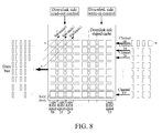
- FIG. 6, FIG. 7 and FIG. 8 The block diagrams for implementing the embodiments of the present invention are shown in FIG. 6, FIG. 7 and FIG. 8 .
- the uplink and downlink shared caches both consist of N pieces of simple dual-port RAM, and each piece of RAM is logically divided into Y RAM segments.
- the RAM segments in the same column correspond to the same channel, and are called a RAM segment column.
- the shared cache divides an address range for each logical RAM segment, and in the process of performing reading or writing operation on the shared cache, respective RAM segments are distinguished through the reading and writing addresses; each logical RAM segment is read and write controlled according to a fixed timeslot, and when it is selected and the read enable is pulled up, the data in the first portion of the RAM segment are output, and when it is selected and the write enable is to pulled up, the data are written into the end portion of the RAM segment.
- the uplink side write-in control module After each data is written in completely, the uplink side write-in control module will record the current write-in end position (written to which RAM segment in the RAM segment column) for the written RAM segment column. In each write-in, the uplink side write-in control module selects a corresponding RAM segment column according to the destination indication, and then takes the RAM segment column of "the last write-in end position + 1" as the start position of the current write-in, and according to the valid bit field indication of the data, determine to pull up the write enable of the "valid bit field” RAM pieces in turn from the start position of the current write-in. The valid data on the data bus will also be sequentially sent to the respective RAM segments currently selected from the start position of the current write-in.
- the valid bit field lengths of the second data and the third data that are sequentially destined for the channel m# are 4B and 8B, respectively.
- the write-in end position of the RAM segment column m# corresponding to the channel m# is RAM segment #1.
- the data When writing in the first data, the data is sequentially stored into RAM segment 2# ⁇ RAM segment 5# from the beginning to the end, and after the write-in is completed, the write-in end position of the RAM segment column m# is updated as RAM segment 5#; when writing in the second data, the data is sequentially stored from the beginning to the end into RAM segment 5#, RAM segment 6#, RAM segment 7#, RAM segment 0#, RAM segment 1#, and RAM segment #2, and after the write-in is completed, the write-in end position of the RAM segment column m# is updated as RAM segment #2.
- each RAM segment column will record its last read-out end position, and if the position of a RAM segment currently being polled is "the last read-out end position of the RAM segment column + 1", and the RAM segment is not empty and meanwhile its corresponding output channel currently can receive data, then the read enable of the RAM piece where the RAM segment is located is pulled high, and the data read out at this time are sent to a channel corresponding to the RAM; and in the other cases, no data is output.
- FIG. 8 The entire write-in and read-out processes on the downlink side are shown as FIG. 8 .
- the downlink side write-in control module records the last write-in position for each RAM segment column. If the position of a RAM segment currently being polled is "the last write-in position of the RAM segment column+1", and the RAM segment has spare space and meanwhile its corresponding channel has data to output, then the write enable of the RAM piece where the RAM segment is located is pulled up, and the data input from the corresponding channel are sent to the RAM segment; and in the other cases, no data write-in operation is performed.
- each module/unit in the abovementioned embodiments may be realized in a form of hardware, or in a form of software function modules.
- the present invention is not limited to any specific form of hardware and software combinations.
Landscapes
- Engineering & Computer Science (AREA)
- Theoretical Computer Science (AREA)
- Physics & Mathematics (AREA)
- General Engineering & Computer Science (AREA)
- General Physics & Mathematics (AREA)
- Memory System Of A Hierarchy Structure (AREA)
- Information Transfer Systems (AREA)
- Time-Division Multiplex Systems (AREA)
- Computer And Data Communications (AREA)
- Communication Control (AREA)
Applications Claiming Priority (2)
| Application Number | Priority Date | Filing Date | Title |
|---|---|---|---|
| CN201210379871.XA CN103714038B (zh) | 2012-10-09 | 2012-10-09 | 一种数据处理方法和装置 |
| PCT/CN2013/084481 WO2014056405A1 (zh) | 2012-10-09 | 2013-09-27 | 一种数据处理方法和装置 |
Publications (3)
| Publication Number | Publication Date |
|---|---|
| EP2908251A1 true EP2908251A1 (de) | 2015-08-19 |
| EP2908251A4 EP2908251A4 (de) | 2015-12-30 |
| EP2908251B1 EP2908251B1 (de) | 2019-06-12 |
Family
ID=50407031
Family Applications (1)
| Application Number | Title | Priority Date | Filing Date |
|---|---|---|---|
| EP13844885.7A Active EP2908251B1 (de) | 2012-10-09 | 2013-09-27 | Verfahren und vorrichtung zur datenzellenverarbeitung |
Country Status (7)
| Country | Link |
|---|---|
| US (1) | US9772946B2 (de) |
| EP (1) | EP2908251B1 (de) |
| JP (1) | JP6077125B2 (de) |
| KR (1) | KR20150067321A (de) |
| CN (1) | CN103714038B (de) |
| ES (1) | ES2749519T3 (de) |
| WO (1) | WO2014056405A1 (de) |
Families Citing this family (11)
| Publication number | Priority date | Publication date | Assignee | Title |
|---|---|---|---|---|
| CN105607888A (zh) * | 2014-11-25 | 2016-05-25 | 中兴通讯股份有限公司 | 数据位宽转换方法及装置 |
| CN104850515B (zh) * | 2015-04-28 | 2018-03-06 | 华为技术有限公司 | 一种缓存信元数据的方法、装置和设备 |
| US10205672B2 (en) * | 2015-09-11 | 2019-02-12 | Cirrus Logic, Inc. | Multi-device synchronization of devices |
| CN107920258B (zh) * | 2016-10-11 | 2020-09-08 | 中国移动通信有限公司研究院 | 一种数据处理方法及装置 |
| CN109388590B (zh) * | 2018-09-28 | 2021-02-26 | 中国电子科技集团公司第五十二研究所 | 提升多通道dma访问性能的动态缓存块管理方法和装置 |
| CN109818603B (zh) * | 2018-12-14 | 2023-04-28 | 深圳市紫光同创电子有限公司 | 一种位宽转换电路的复用方法及位宽转换电路 |
| CN110134365B (zh) * | 2019-05-21 | 2022-10-11 | 合肥工业大学 | 一种多通道并行读出fifo的方法及装置 |
| WO2022110018A1 (zh) * | 2020-11-27 | 2022-06-02 | 西安诺瓦星云科技股份有限公司 | 数据传输方法、装置、通信系统、存储介质和处理器 |
| CN114153763A (zh) * | 2021-11-09 | 2022-03-08 | 中国船舶重工集团公司第七一五研究所 | 一种高带宽低延时算法处理的fpga硬件实现方法 |
| CN115061959B (zh) * | 2022-08-17 | 2022-10-25 | 深圳比特微电子科技有限公司 | 数据交互方法、装置、系统、电子设备和存储介质 |
| WO2024040604A1 (zh) * | 2022-08-26 | 2024-02-29 | 华为技术有限公司 | 一种数据传输方法及装置 |
Family Cites Families (9)
| Publication number | Priority date | Publication date | Assignee | Title |
|---|---|---|---|---|
| US6754741B2 (en) * | 2001-05-10 | 2004-06-22 | Pmc-Sierra, Inc. | Flexible FIFO system for interfacing between datapaths of variable length |
| CN1286029C (zh) * | 2002-08-20 | 2006-11-22 | 华为技术有限公司 | 控制芯片片内存储装置及其存储方法 |
| CN1674477B (zh) | 2004-03-26 | 2010-08-04 | 华为技术有限公司 | 一种实现时分复用电路位宽转换的装置及方法 |
| US7613856B2 (en) * | 2004-10-21 | 2009-11-03 | Lsi Corporation | Arbitrating access for a plurality of data channel inputs with different characteristics |
| US8380943B2 (en) * | 2008-01-07 | 2013-02-19 | Rambus Inc. | Variable-width memory module and buffer |
| CN101291275B (zh) * | 2008-06-02 | 2010-10-06 | 杭州华三通信技术有限公司 | Spi4.2总线桥接实现方法及spi4.2总线桥接器件 |
| CN101789845B (zh) * | 2010-02-22 | 2013-01-16 | 烽火通信科技股份有限公司 | 应用sfec的光传送网中总线位宽变换实现方法及电路 |
| CN101894005A (zh) * | 2010-05-26 | 2010-11-24 | 上海大学 | 高速接口向低速接口的异步fifo传输方法 |
| CN102541506B (zh) * | 2010-12-29 | 2014-02-26 | 深圳市恒扬科技有限公司 | 一种fifo数据缓存器、芯片以及设备 |
-
2012
- 2012-10-09 CN CN201210379871.XA patent/CN103714038B/zh active Active
-
2013
- 2013-09-27 KR KR1020157011938A patent/KR20150067321A/ko not_active Application Discontinuation
- 2013-09-27 WO PCT/CN2013/084481 patent/WO2014056405A1/zh active Application Filing
- 2013-09-27 EP EP13844885.7A patent/EP2908251B1/de active Active
- 2013-09-27 ES ES13844885T patent/ES2749519T3/es active Active
- 2013-09-27 JP JP2015535968A patent/JP6077125B2/ja active Active
- 2013-09-27 US US14/434,564 patent/US9772946B2/en active Active
Also Published As
| Publication number | Publication date |
|---|---|
| US20150301943A1 (en) | 2015-10-22 |
| CN103714038A (zh) | 2014-04-09 |
| JP2016503526A (ja) | 2016-02-04 |
| US9772946B2 (en) | 2017-09-26 |
| CN103714038B (zh) | 2019-02-15 |
| EP2908251A4 (de) | 2015-12-30 |
| EP2908251B1 (de) | 2019-06-12 |
| ES2749519T3 (es) | 2020-03-20 |
| KR20150067321A (ko) | 2015-06-17 |
| JP6077125B2 (ja) | 2017-02-08 |
| WO2014056405A1 (zh) | 2014-04-17 |
Similar Documents
| Publication | Publication Date | Title |
|---|---|---|
| EP2908251B1 (de) | Verfahren und vorrichtung zur datenzellenverarbeitung | |
| US8225026B2 (en) | Data packet access control apparatus and method thereof | |
| CN110134366B (zh) | 一种并行写入多通道fifo的方法及装置 | |
| US10205673B2 (en) | Data caching method and device, and storage medium | |
| CN112703489A (zh) | 控制器、存储器件访问系统、电子设备和数据传输方法 | |
| CN105573922B (zh) | 一种实现数据格式转换的方法和装置 | |
| CN105335323A (zh) | 一种数据突发的缓存装置和方法 | |
| US20190065103A1 (en) | Transmission device and transmission method | |
| CN103117962B (zh) | 一种星载共享存储交换装置 | |
| CN104468156B (zh) | 一种利用时隙仲裁节省资源开销的方法和设备 | |
| CN105446699A (zh) | 数据帧队列管理方法 | |
| CN105577985A (zh) | 一种数字图像处理系统 | |
| US10031884B2 (en) | Storage apparatus and method for processing plurality of pieces of client data | |
| CN102571535B (zh) | 一种数据延迟装置、方法及通信系统 | |
| CN113254387B (zh) | 数据缓存器、芯片、机器人、数据缓存方法 | |
| US20120203982A1 (en) | Fifo buffer and method of controlling fifo buffer | |
| KR102338872B1 (ko) | 다수의 클라이언트 데이터를 처리하는 저장 장치 및 방법 | |
| CN107092440B (zh) | 一种基于fpga的irig106高速数据存储系统 | |
| CN111831209A (zh) | 数据存取装置及系统 | |
| CN104850515B (zh) | 一种缓存信元数据的方法、装置和设备 | |
| CN105930286B (zh) | 一种使用在otn分组交换接口芯片内部的分时存储电路结构 | |
| JP2013162475A (ja) | ループバック回路 | |
| CN117119579B (zh) | 天线数据的处理方法、装置、设备及存储介质 | |
| WO2021120132A1 (zh) | 一种存储系统及数据交叉方法 | |
| WO2014208489A1 (ja) | パケット転送処理装置および方法 |
Legal Events
| Date | Code | Title | Description |
|---|---|---|---|
| PUAI | Public reference made under article 153(3) epc to a published international application that has entered the european phase |
Free format text: ORIGINAL CODE: 0009012 |
|
| 17P | Request for examination filed |
Effective date: 20150508 |
|
| AK | Designated contracting states |
Kind code of ref document: A1 Designated state(s): AL AT BE BG CH CY CZ DE DK EE ES FI FR GB GR HR HU IE IS IT LI LT LU LV MC MK MT NL NO PL PT RO RS SE SI SK SM TR |
|
| AX | Request for extension of the european patent |
Extension state: BA ME |
|
| RA4 | Supplementary search report drawn up and despatched (corrected) |
Effective date: 20151201 |
|
| RIC1 | Information provided on ipc code assigned before grant |
Ipc: G06F 15/167 20060101AFI20151125BHEP Ipc: G06F 12/08 20060101ALI20151125BHEP Ipc: G06F 13/16 20060101ALI20151125BHEP |
|
| DAX | Request for extension of the european patent (deleted) | ||
| GRAP | Despatch of communication of intention to grant a patent |
Free format text: ORIGINAL CODE: EPIDOSNIGR1 |
|
| STAA | Information on the status of an ep patent application or granted ep patent |
Free format text: STATUS: GRANT OF PATENT IS INTENDED |
|
| INTG | Intention to grant announced |
Effective date: 20190103 |
|
| GRAS | Grant fee paid |
Free format text: ORIGINAL CODE: EPIDOSNIGR3 |
|
| GRAA | (expected) grant |
Free format text: ORIGINAL CODE: 0009210 |
|
| STAA | Information on the status of an ep patent application or granted ep patent |
Free format text: STATUS: THE PATENT HAS BEEN GRANTED |
|
| AK | Designated contracting states |
Kind code of ref document: B1 Designated state(s): AL AT BE BG CH CY CZ DE DK EE ES FI FR GB GR HR HU IE IS IT LI LT LU LV MC MK MT NL NO PL PT RO RS SE SI SK SM TR |
|
| REG | Reference to a national code |
Ref country code: GB Ref legal event code: FG4D |
|
| REG | Reference to a national code |
Ref country code: CH Ref legal event code: EP |
|
| REG | Reference to a national code |
Ref country code: AT Ref legal event code: REF Ref document number: 1143487 Country of ref document: AT Kind code of ref document: T Effective date: 20190615 |
|
| REG | Reference to a national code |
Ref country code: IE Ref legal event code: FG4D |
|
| REG | Reference to a national code |
Ref country code: DE Ref legal event code: R096 Ref document number: 602013056642 Country of ref document: DE |
|
| REG | Reference to a national code |
Ref country code: NL Ref legal event code: MP Effective date: 20190612 |
|
| REG | Reference to a national code |
Ref country code: LT Ref legal event code: MG4D |
|
| PG25 | Lapsed in a contracting state [announced via postgrant information from national office to epo] |
Ref country code: SE Free format text: LAPSE BECAUSE OF FAILURE TO SUBMIT A TRANSLATION OF THE DESCRIPTION OR TO PAY THE FEE WITHIN THE PRESCRIBED TIME-LIMIT Effective date: 20190612 Ref country code: HR Free format text: LAPSE BECAUSE OF FAILURE TO SUBMIT A TRANSLATION OF THE DESCRIPTION OR TO PAY THE FEE WITHIN THE PRESCRIBED TIME-LIMIT Effective date: 20190612 Ref country code: AL Free format text: LAPSE BECAUSE OF FAILURE TO SUBMIT A TRANSLATION OF THE DESCRIPTION OR TO PAY THE FEE WITHIN THE PRESCRIBED TIME-LIMIT Effective date: 20190612 Ref country code: NO Free format text: LAPSE BECAUSE OF FAILURE TO SUBMIT A TRANSLATION OF THE DESCRIPTION OR TO PAY THE FEE WITHIN THE PRESCRIBED TIME-LIMIT Effective date: 20190912 Ref country code: FI Free format text: LAPSE BECAUSE OF FAILURE TO SUBMIT A TRANSLATION OF THE DESCRIPTION OR TO PAY THE FEE WITHIN THE PRESCRIBED TIME-LIMIT Effective date: 20190612 Ref country code: LT Free format text: LAPSE BECAUSE OF FAILURE TO SUBMIT A TRANSLATION OF THE DESCRIPTION OR TO PAY THE FEE WITHIN THE PRESCRIBED TIME-LIMIT Effective date: 20190612 |
|
| PG25 | Lapsed in a contracting state [announced via postgrant information from national office to epo] |
Ref country code: BG Free format text: LAPSE BECAUSE OF FAILURE TO SUBMIT A TRANSLATION OF THE DESCRIPTION OR TO PAY THE FEE WITHIN THE PRESCRIBED TIME-LIMIT Effective date: 20190912 Ref country code: RS Free format text: LAPSE BECAUSE OF FAILURE TO SUBMIT A TRANSLATION OF THE DESCRIPTION OR TO PAY THE FEE WITHIN THE PRESCRIBED TIME-LIMIT Effective date: 20190612 Ref country code: LV Free format text: LAPSE BECAUSE OF FAILURE TO SUBMIT A TRANSLATION OF THE DESCRIPTION OR TO PAY THE FEE WITHIN THE PRESCRIBED TIME-LIMIT Effective date: 20190612 Ref country code: GR Free format text: LAPSE BECAUSE OF FAILURE TO SUBMIT A TRANSLATION OF THE DESCRIPTION OR TO PAY THE FEE WITHIN THE PRESCRIBED TIME-LIMIT Effective date: 20190913 |
|
| REG | Reference to a national code |
Ref country code: AT Ref legal event code: MK05 Ref document number: 1143487 Country of ref document: AT Kind code of ref document: T Effective date: 20190612 |
|
| PG25 | Lapsed in a contracting state [announced via postgrant information from national office to epo] |
Ref country code: NL Free format text: LAPSE BECAUSE OF FAILURE TO SUBMIT A TRANSLATION OF THE DESCRIPTION OR TO PAY THE FEE WITHIN THE PRESCRIBED TIME-LIMIT Effective date: 20190612 Ref country code: AT Free format text: LAPSE BECAUSE OF FAILURE TO SUBMIT A TRANSLATION OF THE DESCRIPTION OR TO PAY THE FEE WITHIN THE PRESCRIBED TIME-LIMIT Effective date: 20190612 Ref country code: EE Free format text: LAPSE BECAUSE OF FAILURE TO SUBMIT A TRANSLATION OF THE DESCRIPTION OR TO PAY THE FEE WITHIN THE PRESCRIBED TIME-LIMIT Effective date: 20190612 Ref country code: CZ Free format text: LAPSE BECAUSE OF FAILURE TO SUBMIT A TRANSLATION OF THE DESCRIPTION OR TO PAY THE FEE WITHIN THE PRESCRIBED TIME-LIMIT Effective date: 20190612 Ref country code: SK Free format text: LAPSE BECAUSE OF FAILURE TO SUBMIT A TRANSLATION OF THE DESCRIPTION OR TO PAY THE FEE WITHIN THE PRESCRIBED TIME-LIMIT Effective date: 20190612 Ref country code: RO Free format text: LAPSE BECAUSE OF FAILURE TO SUBMIT A TRANSLATION OF THE DESCRIPTION OR TO PAY THE FEE WITHIN THE PRESCRIBED TIME-LIMIT Effective date: 20190612 Ref country code: PT Free format text: LAPSE BECAUSE OF FAILURE TO SUBMIT A TRANSLATION OF THE DESCRIPTION OR TO PAY THE FEE WITHIN THE PRESCRIBED TIME-LIMIT Effective date: 20191014 |
|
| PG25 | Lapsed in a contracting state [announced via postgrant information from national office to epo] |
Ref country code: IS Free format text: LAPSE BECAUSE OF FAILURE TO SUBMIT A TRANSLATION OF THE DESCRIPTION OR TO PAY THE FEE WITHIN THE PRESCRIBED TIME-LIMIT Effective date: 20191012 Ref country code: SM Free format text: LAPSE BECAUSE OF FAILURE TO SUBMIT A TRANSLATION OF THE DESCRIPTION OR TO PAY THE FEE WITHIN THE PRESCRIBED TIME-LIMIT Effective date: 20190612 |
|
| REG | Reference to a national code |
Ref country code: DE Ref legal event code: R097 Ref document number: 602013056642 Country of ref document: DE |
|
| REG | Reference to a national code |
Ref country code: ES Ref legal event code: FG2A Ref document number: 2749519 Country of ref document: ES Kind code of ref document: T3 Effective date: 20200320 |
|
| PG25 | Lapsed in a contracting state [announced via postgrant information from national office to epo] |
Ref country code: TR Free format text: LAPSE BECAUSE OF FAILURE TO SUBMIT A TRANSLATION OF THE DESCRIPTION OR TO PAY THE FEE WITHIN THE PRESCRIBED TIME-LIMIT Effective date: 20190612 |
|
| PLBE | No opposition filed within time limit |
Free format text: ORIGINAL CODE: 0009261 |
|
| STAA | Information on the status of an ep patent application or granted ep patent |
Free format text: STATUS: NO OPPOSITION FILED WITHIN TIME LIMIT |
|
| PG25 | Lapsed in a contracting state [announced via postgrant information from national office to epo] |
Ref country code: DK Free format text: LAPSE BECAUSE OF FAILURE TO SUBMIT A TRANSLATION OF THE DESCRIPTION OR TO PAY THE FEE WITHIN THE PRESCRIBED TIME-LIMIT Effective date: 20190612 Ref country code: PL Free format text: LAPSE BECAUSE OF FAILURE TO SUBMIT A TRANSLATION OF THE DESCRIPTION OR TO PAY THE FEE WITHIN THE PRESCRIBED TIME-LIMIT Effective date: 20190612 |
|
| 26N | No opposition filed |
Effective date: 20200313 |
|
| PG25 | Lapsed in a contracting state [announced via postgrant information from national office to epo] |
Ref country code: IS Free format text: LAPSE BECAUSE OF FAILURE TO SUBMIT A TRANSLATION OF THE DESCRIPTION OR TO PAY THE FEE WITHIN THE PRESCRIBED TIME-LIMIT Effective date: 20200224 Ref country code: SI Free format text: LAPSE BECAUSE OF FAILURE TO SUBMIT A TRANSLATION OF THE DESCRIPTION OR TO PAY THE FEE WITHIN THE PRESCRIBED TIME-LIMIT Effective date: 20190612 Ref country code: MC Free format text: LAPSE BECAUSE OF FAILURE TO SUBMIT A TRANSLATION OF THE DESCRIPTION OR TO PAY THE FEE WITHIN THE PRESCRIBED TIME-LIMIT Effective date: 20190612 |
|
| REG | Reference to a national code |
Ref country code: CH Ref legal event code: PL |
|
| PG2D | Information on lapse in contracting state deleted |
Ref country code: IS |
|
| PG25 | Lapsed in a contracting state [announced via postgrant information from national office to epo] |
Ref country code: CH Free format text: LAPSE BECAUSE OF NON-PAYMENT OF DUE FEES Effective date: 20190930 Ref country code: LU Free format text: LAPSE BECAUSE OF NON-PAYMENT OF DUE FEES Effective date: 20190927 Ref country code: IE Free format text: LAPSE BECAUSE OF NON-PAYMENT OF DUE FEES Effective date: 20190927 Ref country code: LI Free format text: LAPSE BECAUSE OF NON-PAYMENT OF DUE FEES Effective date: 20190930 |
|
| REG | Reference to a national code |
Ref country code: BE Ref legal event code: MM Effective date: 20190930 |
|
| PG25 | Lapsed in a contracting state [announced via postgrant information from national office to epo] |
Ref country code: BE Free format text: LAPSE BECAUSE OF NON-PAYMENT OF DUE FEES Effective date: 20190930 |
|
| PG25 | Lapsed in a contracting state [announced via postgrant information from national office to epo] |
Ref country code: CY Free format text: LAPSE BECAUSE OF FAILURE TO SUBMIT A TRANSLATION OF THE DESCRIPTION OR TO PAY THE FEE WITHIN THE PRESCRIBED TIME-LIMIT Effective date: 20190612 |
|
| PG25 | Lapsed in a contracting state [announced via postgrant information from national office to epo] |
Ref country code: HU Free format text: LAPSE BECAUSE OF FAILURE TO SUBMIT A TRANSLATION OF THE DESCRIPTION OR TO PAY THE FEE WITHIN THE PRESCRIBED TIME-LIMIT; INVALID AB INITIO Effective date: 20130927 Ref country code: MT Free format text: LAPSE BECAUSE OF FAILURE TO SUBMIT A TRANSLATION OF THE DESCRIPTION OR TO PAY THE FEE WITHIN THE PRESCRIBED TIME-LIMIT Effective date: 20190612 |
|
| PG25 | Lapsed in a contracting state [announced via postgrant information from national office to epo] |
Ref country code: MK Free format text: LAPSE BECAUSE OF FAILURE TO SUBMIT A TRANSLATION OF THE DESCRIPTION OR TO PAY THE FEE WITHIN THE PRESCRIBED TIME-LIMIT Effective date: 20190612 |
|
| REG | Reference to a national code |
Ref country code: DE Ref legal event code: R081 Ref document number: 602013056642 Country of ref document: DE Owner name: SANECHIPS TECHNOLOGY CO., LTD., SHENZHEN, CN Free format text: FORMER OWNER: ZTE CORPORATION, SHENZHEN, GUANGDONG, CN Ref country code: DE Ref legal event code: R082 Ref document number: 602013056642 Country of ref document: DE Representative=s name: PATENTANWAELTE CANZLER & BERGMEIER PARTNERSCHA, DE Ref country code: DE Ref legal event code: R082 Ref document number: 602013056642 Country of ref document: DE Representative=s name: CANZLER & BERGMEIER PATENTANWAELTE PARTNERSCHA, DE |
|
| REG | Reference to a national code |
Ref country code: GB Ref legal event code: 732E Free format text: REGISTERED BETWEEN 20230406 AND 20230412 |
|
| REG | Reference to a national code |
Ref country code: ES Ref legal event code: PC2A Owner name: SANECHIPS TECHNOLOGY CO., LTD Effective date: 20230608 |
|
| PGFP | Annual fee paid to national office [announced via postgrant information from national office to epo] |
Ref country code: IT Payment date: 20230810 Year of fee payment: 11 Ref country code: GB Payment date: 20230803 Year of fee payment: 11 |
|
| PGFP | Annual fee paid to national office [announced via postgrant information from national office to epo] |
Ref country code: FR Payment date: 20230808 Year of fee payment: 11 Ref country code: DE Payment date: 20230802 Year of fee payment: 11 |
|
| PGFP | Annual fee paid to national office [announced via postgrant information from national office to epo] |
Ref country code: ES Payment date: 20231005 Year of fee payment: 11 |