EP2901101B1 - Measuring method - Google Patents
Measuring method Download PDFInfo
- Publication number
- EP2901101B1 EP2901101B1 EP13776953.5A EP13776953A EP2901101B1 EP 2901101 B1 EP2901101 B1 EP 2901101B1 EP 13776953 A EP13776953 A EP 13776953A EP 2901101 B1 EP2901101 B1 EP 2901101B1
- Authority
- EP
- European Patent Office
- Prior art keywords
- wave
- optical element
- waves
- spherical
- output
- Prior art date
- Legal status (The legal status is an assumption and is not a legal conclusion. Google has not performed a legal analysis and makes no representation as to the accuracy of the status listed.)
- Active
Links
- 238000000034 method Methods 0.000 title claims description 28
- 230000003287 optical effect Effects 0.000 claims description 189
- 238000005259 measurement Methods 0.000 claims description 89
- 238000012937 correction Methods 0.000 claims description 27
- 230000003993 interaction Effects 0.000 claims description 10
- 239000013598 vector Substances 0.000 description 24
- 239000000758 substrate Substances 0.000 description 22
- 230000005855 radiation Effects 0.000 description 16
- 238000004519 manufacturing process Methods 0.000 description 13
- 230000000737 periodic effect Effects 0.000 description 12
- 238000005286 illumination Methods 0.000 description 11
- 238000011156 evaluation Methods 0.000 description 9
- 230000000052 comparative effect Effects 0.000 description 8
- 238000012360 testing method Methods 0.000 description 6
- 238000001514 detection method Methods 0.000 description 5
- 238000010586 diagram Methods 0.000 description 5
- 230000010355 oscillation Effects 0.000 description 5
- 238000004364 calculation method Methods 0.000 description 3
- 238000013461 design Methods 0.000 description 3
- 230000000694 effects Effects 0.000 description 3
- 238000005305 interferometry Methods 0.000 description 3
- 238000012935 Averaging Methods 0.000 description 2
- 230000001427 coherent effect Effects 0.000 description 2
- CPBQJMYROZQQJC-UHFFFAOYSA-N helium neon Chemical compound [He].[Ne] CPBQJMYROZQQJC-UHFFFAOYSA-N 0.000 description 2
- 230000005670 electromagnetic radiation Effects 0.000 description 1
- 238000001900 extreme ultraviolet lithography Methods 0.000 description 1
- 230000002452 interceptive effect Effects 0.000 description 1
- 238000012545 processing Methods 0.000 description 1
- 230000035945 sensitivity Effects 0.000 description 1
- 238000010008 shearing Methods 0.000 description 1
Images


Classifications
-
- G—PHYSICS
- G01—MEASURING; TESTING
- G01B—MEASURING LENGTH, THICKNESS OR SIMILAR LINEAR DIMENSIONS; MEASURING ANGLES; MEASURING AREAS; MEASURING IRREGULARITIES OF SURFACES OR CONTOURS
- G01B11/00—Measuring arrangements characterised by the use of optical techniques
- G01B11/24—Measuring arrangements characterised by the use of optical techniques for measuring contours or curvatures
- G01B11/2441—Measuring arrangements characterised by the use of optical techniques for measuring contours or curvatures using interferometry
-
- G—PHYSICS
- G01—MEASURING; TESTING
- G01B—MEASURING LENGTH, THICKNESS OR SIMILAR LINEAR DIMENSIONS; MEASURING ANGLES; MEASURING AREAS; MEASURING IRREGULARITIES OF SURFACES OR CONTOURS
- G01B9/00—Measuring instruments characterised by the use of optical techniques
- G01B9/02—Interferometers
- G01B9/02015—Interferometers characterised by the beam path configuration
- G01B9/02027—Two or more interferometric channels or interferometers
- G01B9/02028—Two or more reference or object arms in one interferometer
-
- G—PHYSICS
- G01—MEASURING; TESTING
- G01B—MEASURING LENGTH, THICKNESS OR SIMILAR LINEAR DIMENSIONS; MEASURING ANGLES; MEASURING AREAS; MEASURING IRREGULARITIES OF SURFACES OR CONTOURS
- G01B9/00—Measuring instruments characterised by the use of optical techniques
- G01B9/02—Interferometers
- G01B9/02034—Interferometers characterised by particularly shaped beams or wavefronts
- G01B9/02038—Shaping the wavefront, e.g. generating a spherical wavefront
- G01B9/02039—Shaping the wavefront, e.g. generating a spherical wavefront by matching the wavefront with a particular object surface shape
-
- G—PHYSICS
- G01—MEASURING; TESTING
- G01B—MEASURING LENGTH, THICKNESS OR SIMILAR LINEAR DIMENSIONS; MEASURING ANGLES; MEASURING AREAS; MEASURING IRREGULARITIES OF SURFACES OR CONTOURS
- G01B9/00—Measuring instruments characterised by the use of optical techniques
- G01B9/02—Interferometers
- G01B9/02055—Reduction or prevention of errors; Testing; Calibration
- G01B9/02056—Passive reduction of errors
- G01B9/02057—Passive reduction of errors by using common path configuration, i.e. reference and object path almost entirely overlapping
-
- G—PHYSICS
- G01—MEASURING; TESTING
- G01B—MEASURING LENGTH, THICKNESS OR SIMILAR LINEAR DIMENSIONS; MEASURING ANGLES; MEASURING AREAS; MEASURING IRREGULARITIES OF SURFACES OR CONTOURS
- G01B9/00—Measuring instruments characterised by the use of optical techniques
- G01B9/02—Interferometers
- G01B9/02055—Reduction or prevention of errors; Testing; Calibration
- G01B9/0207—Error reduction by correction of the measurement signal based on independently determined error sources, e.g. using a reference interferometer
- G01B9/02072—Error reduction by correction of the measurement signal based on independently determined error sources, e.g. using a reference interferometer by calibration or testing of interferometer
-
- G—PHYSICS
- G01—MEASURING; TESTING
- G01M—TESTING STATIC OR DYNAMIC BALANCE OF MACHINES OR STRUCTURES; TESTING OF STRUCTURES OR APPARATUS, NOT OTHERWISE PROVIDED FOR
- G01M11/00—Testing of optical apparatus; Testing structures by optical methods not otherwise provided for
- G01M11/005—Testing of reflective surfaces, e.g. mirrors
-
- G—PHYSICS
- G01—MEASURING; TESTING
- G01M—TESTING STATIC OR DYNAMIC BALANCE OF MACHINES OR STRUCTURES; TESTING OF STRUCTURES OR APPARATUS, NOT OTHERWISE PROVIDED FOR
- G01M11/00—Testing of optical apparatus; Testing structures by optical methods not otherwise provided for
- G01M11/02—Testing optical properties
- G01M11/0242—Testing optical properties by measuring geometrical properties or aberrations
- G01M11/0271—Testing optical properties by measuring geometrical properties or aberrations by using interferometric methods
-
- G—PHYSICS
- G02—OPTICS
- G02B—OPTICAL ELEMENTS, SYSTEMS OR APPARATUS
- G02B5/00—Optical elements other than lenses
- G02B5/18—Diffraction gratings
- G02B5/1866—Transmission gratings characterised by their structure, e.g. step profile, contours of substrate or grooves, pitch variations, materials
- G02B5/1871—Transmissive phase gratings
-
- G—PHYSICS
- G02—OPTICS
- G02B—OPTICAL ELEMENTS, SYSTEMS OR APPARATUS
- G02B5/00—Optical elements other than lenses
- G02B5/32—Holograms used as optical elements
-
- Y—GENERAL TAGGING OF NEW TECHNOLOGICAL DEVELOPMENTS; GENERAL TAGGING OF CROSS-SECTIONAL TECHNOLOGIES SPANNING OVER SEVERAL SECTIONS OF THE IPC; TECHNICAL SUBJECTS COVERED BY FORMER USPC CROSS-REFERENCE ART COLLECTIONS [XRACs] AND DIGESTS
- Y10—TECHNICAL SUBJECTS COVERED BY FORMER USPC
- Y10T—TECHNICAL SUBJECTS COVERED BY FORMER US CLASSIFICATION
- Y10T29/00—Metal working
- Y10T29/49—Method of mechanical manufacture
- Y10T29/49764—Method of mechanical manufacture with testing or indicating
- Y10T29/49771—Quantitative measuring or gauging
Definitions
- the invention relates to a method for determining a deviation of an actual shape from an intended shape of an optical surface of an optical element.
- a device for determining a deviation of an actual shape from an intended shape is described in e.g. US 2010/0177321 A1 .
- This device comprises an interferometer for generating a measurement wave, the wavefront of which is adapted to an aspherical intended shape of the optical surface by means of a diffraction grating.
- the wavefront of the adapted measurement wave is evaluated by interferometry after reflection at the optical surface and the deviation of the actual shape of the optical surface from the intended shape thereof is determined in the process.
- the diffraction grating can for example be a computer-generated hologram (CGH), which is generated by virtue of the design of the interferometer being simulated by a suitable calculation method, such as e.g. a ray tracing method, and, in the process, a phase function of the diffraction grating being calculated such that the latter has a desired function in the beam path of the interferometer arrangement. It is then possible to produce the diffraction grating from the calculated phase function thereof.
- CGH computer-generated hologram
- the accuracy of the shape measurement depends on the accuracy of the CGH.
- a diffractive optical element has a substrate and a diffractive structure pattern arranged on the substrate.
- the diffractive structure pattern is configured to convert a plane or spherical input wave radiated thereon into at least four separate output waves, wherein at least one of the output waves is a non-spherical wave, at least a further one of the output waves is a spherical wave and at least two further ones of the output waves respectively are a plane wave or a spherical wave.
- the aforementioned output waves are thus generated by means of merely a single diffractive optical element, i.e. a diffractive structure pattern which is arranged on a single substrate.
- the diffractive optical element can be configured in accordance with several variants.
- the wave radiated thereon is plane and the output waves comprise at least one non-spherical wave and at least three spherical waves.
- the wave radiated thereon is spherical and the output waves comprise at least one non-spherical wave and at least three spherical waves.
- the wave radiated thereon is plane and the output waves comprise at least one spherical wave and at least two plane waves.
- the wave radiated thereon is spherical and the output waves comprise at least one spherical wave and at least two plane waves.
- the intensities of the spherical waves differ by less than 30%, in particular by less than 10%, from one another in accordance with one embodiment.
- the plane or spherical input wave can be spherical wave only, with, in this case, a plane wave counting as a special case of a spherical wave with an infinite radius.
- the non-spherical output wave can be a measurement wave adapted to an optical surface to be measured, which measurement wave is radiated onto the surface when the latter is measured by interferometric means.
- the further output waves can also be referred to as calibration waves.
- the diffractive optical element is, in particular, embodied as computer-generated hologram (CGH).
- the diffractive structure pattern can also be referred to as phase grating or diffraction grating, although it should be noted that this should not necessarily be understood to mean a regular grating, but rather, in particular, line structures which can have bends, which can, in principle, deviate from one another in terms of their shape and which can have a variable distance between them.
- the diffractive structure pattern is arranged on the substrate of the diffractive optical element, i.e. it is merely arranged on one substrate.
- the diffractive structure pattern is therefore not composed of several sub-patterns which are arranged on different substrates.
- a diffractive structure pattern which generates separate output waves as described above may be configured as a complex encoded phase grating.
- a spherical wave is a wave with a spherical wavefront, i.e. a wave in which the wavefront is formed by at least a spherical surface section.
- a non-spherical wave is a wave, the wavefront of which has a deviation of at least 10 ⁇ from any ideal sphere, in particular from the sphere with the best fit to the wavefront, where ⁇ is the wavelength of the input wave radiated thereon.
- the non-spherical wave has at least one point at which it deviates from every ideal sphere by at least 10 ⁇ . If the wavelength is 500 nm, a non-spherical wave within the meaning of the application has a deviation of at least 5 ⁇ m from any ideal sphere.
- non-spherical waves comprise both waves with rotationally symmetric wavefronts, i.e. aspherical waves in the conventional sense, and waves with non-rotationally symmetric wavefronts, i.e. waves, the wavefronts of which have the shape of so-called free-form surfaces.
- the non-spherical wave has a wavefront in the form of a free-form surface, wherein the wavefront has a deviation of at least 1 mm from any ideal sphere.
- separate output waves should be understood to mean that the output waves have different propagation directions and can therefore be detected or reflected back to the diffractive optical element independently of one another, such that these can be measured separately in an interferometric measurement system.
- the diffractive optical element according to the invention differs in that, according to the invention, at least three further output waves, which are plane or spherical, are generated in addition to the non-spherical output wave.
- at least three further output waves which are plane or spherical, are generated in addition to the non-spherical output wave.
- no more than two plane or spherical waves are generated, in addition to one or more non-spherical waves, in the different orders of diffraction.
- a wave which is formed by a sphere and a non-sphere and which is therefore likewise non-spherical is usually radiated onto the second CGH. If a plane or spherical wave were to be radiated onto this CGH, not a single plane or spherical wave would be generated in the process.
- Generating the at least three further output waves of the aforementioned type in addition to the non-spherical output wave when a plane or spherical input wave is radiated onto the diffractive optical element according to the invention renders it possible for the diffractive optical element to be measured in respect of manufacturing errors by means of the further output waves.
- the structure pattern is configured such that the at least two further output waves are plane waves, the propagation directions of which are symmetrical to one another in relation to a direction of incidence of the input wave.
- the two plane output waves are a positive and negative order of diffraction of the same order, such as e.g. the +1st and -1st order of diffraction, at a linear grating.
- the structure pattern is configured such that, in addition to the two plane output waves forming a first wave pair, the separate output waves have two further plane waves in the form of a second wave pair, the propagation directions of which are likewise symmetrical to one another in relation to the direction of incidence, with a plane spanned by the propagation directions of the first wave pair deviating from the plane spanned by the propagation directions of the second wave pair.
- the plane spanned by the propagation directions of the first wave pair is substantially perpendicular to the plane spanned by the propagation directions of the second wave pair.
- substantially perpendicular means an angle of at least 80°, in particular at least 85°, at least 89° or approximately 90°.
- an angle ⁇ i is defined at every point i of the diffractive structure pattern by the angle between a first difference vector and a second difference vector, the first difference vector being defined by the difference between the wave vector k i (A) of the non-spherical wave emanating from the point i and the wave vector k i (in) of the input wave impinging on the point i and the second difference vector being defined by the difference between the wave vector k i (S) of the at least one spherical wave emanating from the point i and the wave vector k i (in) of the input wave impinging on the point i.
- the structure pattern is configured such that the absolute value of the angle ⁇ i , averaged over the points i of the diffractive structure pattern, is greater than 5°, in particular greater than 10°, in projection onto a plane parallel to the structure pattern.
- the wave vector is also referred to as "k-vector" and is that vector which is perpendicular to the wavefront of a wave.
- N denotes the number of points i over which the mean value is formed.
- the mean is formed over the area covered by the structure pattern, i.e. the optically effective area of the diffractive optical element.
- the propagation direction of the input wave is referred to as the z-direction, and so the xy-plane is the plane perpendicular to the propagation direction of the input wave.
- the diffraction efficiency of the structure pattern for generating the non-spherical wave is at least 50% greater than the diffraction efficiency of the structure pattern for generating the at least one spherical wave.
- the intensity of the non-spherical wave is at least 50% greater than the intensity of the at least one spherical wave.
- the diffraction efficiency for generating the at least one non-spherical wave is at least 70% greater, in particular at least 100% greater, than the diffraction efficiency for generating the at least one spherical wave. This can be compensated for by using metallized calibration mirrors.
- the sum of the diffraction efficiencies of the at least four output waves is greater than 30%.
- the structure pattern is configured such that the radiation power of the non-spherical output wave is greater than the respective radiation power of the spherical or the plane output waves. That is to say, the output wave with the non-spherical wavefront is weighted more strongly in the structure pattern than the remaining three output waves with the spherical or the plane wavefront.
- the radiation power of the output wave with the non-spherical wavefront has at least 30%, in particular approximately 40%, of the radiation power of the input wave and the remaining three output waves with the spherical or the plane wavefront each have between 15% and 25%, in particular approximately 20%, of the radiation power of the input wave.
- the structure pattern is configured such that the input wave radiated thereon is converted into at least five separate output waves, with four of the output waves being embodied as spherical waves.
- a further one of the at least five output waves is the non-spherical wave, in particular a free-form wave.
- the output waves have respective mean propagation directions which are oriented to one another such that the mean propagation directions of the four spherical output waves in pairs are in each case not arranged symmetrical to one another in relation to an axis defined by the mean propagation direction of the non-spherical output wave.
- “not symmetrical” is understood to mean that there is a deviation of at least 1°, in particular of at least 5°, compared to symmetric arrangement.
- the mean propagation direction is that propagation direction which emerges from intensity-weighted averaging of the different propagation directions of each output wave. In accordance with one embodiment variant, this condition applies to at least 90% of all points on the diffractive optical element.
- the diffractive structure pattern comprises a multilevel phase grating.
- a multilevel phase grating is understood to mean a phase grating which has at least one intermediate level between the uppermost and the lowermost level. Hence, such a phase grating has at least three levels.
- a so-called blazed phase grating has so many levels that the profile is represented by inclined surfaces. The use of a multilevel phase grating renders it possible to at least partially compensate or even overcompensate for a loss in diffraction efficiency caused by complex encoding.
- a multilevel phase grating should also be understood to mean such a blazed phase grating.
- a person skilled in the art can obtain background information in respect of multilevel phase gratings from the handbook by Donald C. O'Shea et al. "Diffractive optics: design, fabrication, and test", 2004, The Society of Photo-Optical Instrumentation Engineers, pages 29 to 35 .
- a multilevel phase grating within the meaning of the application is, in particular, also understood to mean a laterally blazed phase grating, such as described e.g. in the H. Kleemann et al., "Combination of blazed and laterally blazed structures", Diffractive Optics and Micro-Optics, OSA Technical Digest (Optical Society of America), paper DTuC7, 2004 .
- a diffractive optical element which comprises a substrate and a diffraction grating arranged thereon.
- the diffraction grating has grating lines arranged at a distance from one another, a mean periodic distance of the diffraction grating being determined by a center-to-center distance, averaged over the diffraction grating, between in each case neighboring grating lines.
- the grating lines having a wave-like form such that a mean wave period of the grating lines lies in the region between 3 times and 20 times the mean periodic distance of the diffraction grating and a variation in the grating lines transversely to their longitudinal extent has a span which lies in the region between 0.1 times and 3 times the mean periodic distance of the diffraction grating.
- the mean periodic distance of the diffraction grating is measured in the transverse direction of the grating lines.
- a waved form of the grating lines is understood to mean that the grating lines deviate upward and downward, i.e. transversely to the longitudinal extent of the grating lines, in relation to a respective straight line.
- the wave period can vary from deflection to deflection.
- the span of the variation of the grating lines transversely to the longitudinal extent thereof should be understood to mean a span of the deviations of the respective grating line from its imagined straight shape, i.e. from the straight line with the best fit to the respective grating line.
- the span of the variation is twice the amplitude of a wave determining the grating line shape.
- the diffraction grating covers at least 20% of the substrate. If the substrate has a plate- shaped design, 20% of the upper side and lower side, respectively, of the substrate are covered by the diffraction grating.
- At least 90%, in particular at least 95% or at least 99%, of the grating lines of the diffraction grating are embodied as continuous lines which extend without interruption between edge regions of the diffraction grating, i.e. these lines do not end within the area of the substrate covered by the diffraction grating.
- the diffraction grating is configured such that a stripe density of the grating lines averaged within a square measurement area of the diffraction grating with 1 mm edge length over any square partial area with 50 ⁇ m edge length has a variation which extends over a span of less than 20 line pairs/mm.
- the sum of the width of the grating line and the width of the intermediate space, adjoining on one side, to the next grating line is initially determined every 1 ⁇ m along each grating line. The inverse of the value determined thereby is formed and hence the stripe density is established at the relevant measurement point.
- the variation of the mean stripe density has a span of less than 20 line pairs/mm, i.e. the mean stripe densities established for the various partial areas within the measurement area vary by less than 20 line pairs/mm.
- the stripe density on average is approximately 200 lines/mm, the stripe density varies within the span of 190 to 210 lines/mm.
- the structure pattern is configured such that, in addition to the at least four separate output waves, a reference wave in Littrow reflection is also generated as reference wave from the input wave radiated thereon, which reference wave can be used as a reference during an interferometric measurement.
- a diffractive optical element which has a substrate and a diffractive structure pattern arranged thereon.
- the diffractive structure pattern is configured such that the structure pattern converts a plane or spherical input wave radiated thereon into at least three separate output waves with in each case a spherical wavefront.
- this diffractive optical element can contain features from above-described embodiments of the diffractive optical element generating at least four separate output waves.
- a method for determining a deviation of an actual shape from an intended shape of an optical surface of an optical element comprises the following steps: generating an input wave, arranging a diffractive optical element in the beam path of the input wave and converting the input wave into at least three separate output waves by interaction with the diffractive optical element, wherein one of the output waves is a measurement wave, adapted to the intended shape of the optical surface, with a non-spherical wavefront, and at least two further ones of the output waves are calibration waves.
- the method further comprises the steps of determining calibration corrections of the diffractive optical element by means of each one of the at least two calibration waves, arranging the optical surface in the beam path of the adapted wave and measuring the wavefront of the adapted measurement wave after interaction with the optical surface, wherein the wavefront of the adapted measurement wave is measured with the diffractive optical element being oriented in respect of the input wave the same as during the determining of the calibration corrections. Further, according to the above method the measured wavefront is corrected by means of the determined calibration corrections.
- the diffractive optical element is arranged in respect of the propagation direction of the input wave in a given orientation for determining the calibration corrections, wherein the calibration corrections are determined by analyzing each one of the at least two calibration waves.
- This orientation is unchanged when measuring the wavefront of the adapted wave.
- the input wave has the same direction of incidence in the local coordinate system of the diffractive optical element when generating and analyzing the measurement wave and when generating and analyzing the calibration waves.
- the output waves are especially generated simultaneously by interaction of the input wave with the diffractive optical element.
- the determined calibration corrections can be applied directly to the measured wavefront of the adapted wave.
- the determined calibration corrections precisely reflect the manufacturing errors of the diffractive optical element relevant to the generation of the measurement wave. In different words, no errors are introduced into the correction of the wavefront due to a deviation between the measured calibration corrections and the real deviations of the structure on the diffractive optical element generating the measurement wave, which deviation would be due to a different orientation of the diffractive optical element.
- the wavefront of the adapted measurement wave is measured with the diffractive optical element being arranged in the same position in respect of the input wave as during the determining of the calibration corrections. That means both the orientation and the position of the diffractive optical element remains unchanged when measuring the wavefront of the adapted measurement wave.
- the at least two calibration waves include a first calibration wave and a second calibration wave.
- the calibration corrections of the diffractive optical element are determined by means of the first calibration wave and by means of the second calibration wave.
- the determining of calibration corrections includes determining first calibration corrections from a first one of the calibration waves and second calibration corrections from a second one of the calibration waves, wherein the first calibration corrections and the second calibration corrections are determined with the diffractive optical element being oriented the same in respect of the input wave, i.e. the orientation of the diffractive optical element is unchanged between determining the first calibration corrections and the second calibration corrections.
- the diffractive optical element comprises a complex encoded phase grating.
- a complex encoded phase grating is configured with at least three phase functions f 1 to f 3 such that respective diffracted waves are generated for each individual one of the various phase functions f 1 to f 3 , which diffracted waves form the above mentioned output waves.
- the diffracted waves generated for each of the phase functions f 1 to f 3 are each waves generated in the first diffraction order at the phase grating f G .
- the properties of a complex encoded phase grating according to the application is decribed in more detail in the subsequent detailed description of exemplary embodiments.
- the use of a complex encoded phase grating allows to configure the diffractive optical element such that the output waves have different intensities. This may be done by assigning different weights to the individual phase functions f 1 to f 3 within the complex encoded phase grating.
- each one of the at least three output waves are generated in the same diffraction order at the diffractive optical element.
- each one of the at least three output waves are generated in first diffraction order, in particular +1 st diffraction order, at the diffractive optical element.
- first diffraction order in particular +1 st diffraction order
- waves form the output waves.
- calibration waves having a simple geometrical shape, such as a plane or a spherical shape, can be generated. With such simple geometrical shapes a precise calibration can be accomplished, as appropriate calibration objects can be manufactured with high precision.
- the output waves have respective mean propagation directions which are oriented to one another such that the mean propagation directions of the at least two calibration waves are arranged asymmetrically, i.e. are not arranged symmetrical, to one another in relation to an axis defined by the mean propagation direction of the measurement wave.
- At least one of the calibration waves is a spherical wave.
- at least two or at least three calibration waves are spherical waves.
- the input wave is a plane or spherical wave
- the input wave is converted into at least four separate output waves by interaction with the diffractive optical element, wherein at least one further one of the output waves is a calibration wave with spherical wavefront and at least two further ones of the output waves are calibration waves with, in each case, a plane or a spherical wavefront.
- the calibration corrections of the diffractive optical element are determined by means of the three calibration waves.
- the diffractive optical element in any one of the described embodiments, especially to the diffractive optical element configured to convert an input wave into at least four separate output waves, and vice versa.
- the diffractive optical element may be configured to generate the four separate output waves such that a wavefront of the non-spherical wave after interaction with an optical surface may be measured with the diffractive optical element being oriented in respect of the input wave the same as during a determining of calibration corrections by means of the other output waves.
- the diffractive optical element is configured to generate the four separate output waves simultaneously, especially such to generate each one of the output waves in first diffraction order.
- the method according to the invention comprises the following steps: generating a plane or spherical input wave, arranging a diffractive optical element in the beam path of the input wave and converting the input wave into at least four separate output waves by interaction with the diffractive optical element, wherein at least one of the output waves is a measurement wave, adapted to the intended shape of the optical surface, with a non-spherical wavefront, at least one further one of the output waves is a calibration wave with spherical wavefront and at least two further ones of the output waves are calibration waves with, in each case, a plane or a spherical wavefront.
- calibration corrections of the diffractive optical element are determined by means of the calibration waves, the optical surface is measured in the beam path of the adapted measurement wave and the wavefront of the adapted measurement wave is measured after interaction with the optical surface. Furthermore, the measured wavefront is corrected by means of the determined calibration corrections. It is now possible to determine the deviation of the actual shape of the optical surface from the intended shape by means of the corrected wavefront.
- the diffractive optical element used in the method according to the invention can, in particular, be embodied in accordance with one of the above-described embodiments of the comparative examples.
- one or more calibration objects are arranged in the beam paths of the calibration waves and there is an interferometric evaluation of the calibration waves after interaction with the calibration object or objects.
- this method comprises the step of manufacturing the optical element with an optical surface which has a diameter of greater than 500 mm. Furthermore, an actual shape of the optical surface is measured so accurately in relation to an intended shape by interferometry using merely one diffractive optical element that deviations of the actual shape from the intended shape, which trace back to oscillations with vibration wavelengths of between d/100 and d/5, are determined with an accuracy of 0.05 nm, the intended shape being a free-form surface, which has a deviation from each rotationally symmetric asphere of more than 5 ⁇ m. Furthermore, the optical surface is adapted to the intended shape by mechanical processing of the optical surface on the basis of the interferometric measurement result. Adapting the optical surface to the intended shape in this case occurs within the scope of the measurement accuracy of the interferometric measurement.
- the interferometric measurement of the actual shape of the optical surface can, in particular, take place by carrying out the above-described measuring method in one of the embodiments according to the invention.
- the diffractive optical element used in the production method can, in particular, be embodied in one of the above-described embodiments.
- an optical element which has an optical surface with a diameter d of greater than 500 mm.
- an actual shape of the optical surface is adapted to an intended shape such that deviations of the actual shape from the intended shape, which trace back to oscillations with vibration wavelengths of between d/100 and d/5, are no more than 0.05 nm, in particular no more than 0.02 nm.
- the intended shape is a free-form surface, which has a deviation from each rotationally symmetric asphere of more than 5 ⁇ m, in particular of more than 10 ⁇ m.
- the optical element can be embodied as EUV mirror.
- the deviation of the intended shape from the rotationally symmetric asphere with the best fit thereto is more than 5 ⁇ m, in particular more than 10 ⁇ m.
- the optical surface can have a diameter of more than 1000 mm and all oscillations can relate to vibration wavelengths of between 1 mm and 50 mm.
- the intended shape has a deviation from every sphere of at least 1 mm.
- the optical surface is a large or strong free-form surface.
- deviations of the actual shape from the intended shape are defined by the largest amplitude of the deviations of the actual shape from the intended shape at any point on the optical surface.
- a Cartesian xyz-coordinate system is indicated in the drawing, which system reveals the respective positional relationship of the components illustrated in the figures.
- the x-direction extends perpendicularly to the plane of the drawing and into the latter, the y-direction extends upward and the z-direction extends toward the right.
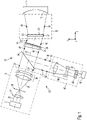
- Figure 1 depicts an interferometric measurement system 10 in one embodiment according to the invention.
- the measurement system 10 is suitable for determining a deviation of an actual shape from a non-spherical intended shape of an optical surface 12 of a test object in the form of an optical element 14.
- the optical element 14 can be embodied in the form of an optical lens element or of a mirror.
- the optical element 14 is a concave mirror for the EUV lithography, i.e. a mirror which, in a microlithographic projection exposure apparatus, is designed with an exposure wavelength in the EUV wavelength range.
- the EUV wavelength range extends to wavelengths below 100 nm and relates, in particular, to wavelengths of approximately 13.5 nm and/or approximately 6.8 nm.
- the optical element 14 is assembled in the measurement system 10 by means of a holder not depicted in the drawing.
- the non-spherical intended shape of the optical surface 12 can have the shape of a rotationally symmetric asphere or a free-form surface, as described in more detail in the general description.
- the interferometric measurement system 10 comprises an interferometer 16, which in turn comprises a light source 18, a beam splitter 34 and an interferometer camera 45.
- the light source 18 generates illumination radiation 20 and, to this end, it comprises a laser 21, such as a helium neon laser, for generating a laser beam 22.
- the illumination radiation 20 has sufficiently coherent light for carrying out an interferometric measurement. In the case of a helium neon laser, the wavelength of the illumination radiation 20 is approximately 633 nm. However, the wavelength of the illumination radiation 20 can also have different wavelengths in the visible and non-visible wavelength range of electromagnetic radiation.
- the laser beam 22 is focused onto a stop 26 by a focusing lens element 24 in such a way that a divergent beam of coherent light emanates from the aperture.
- the wavefront of the divergent beam 28 is substantially spherical.
- the divergent beam 28 is collimated by a lens-element group 30, as a result of which the illumination radiation 20 is generated by a substantially plane wavefront in the present case.
- the illumination radiation 20 propagates along an optical axis 32 of the interferometer 16 and passes through the beam splitter 34.
- the illumination radiation 20 is thereupon incident on a Fizeau element 36 with a Fizeau area 38. A part of the light of the illumination radiation 20 is reflected at the Fizeau area 38 as reference wave 40.
- the light of the illumination radiation 20 passing through the Fizeau element 36 propagates as an input wave 42, with a plane wavefront 44 along the optical axis 32 and is incident on a diffractive optical element 50.
- the wavefront of the input wave 42 can also be spherical.
- the diffractive optical element 50 comprises a transmissive substrate 52 and, arranged on the substrate 52, a diffractive structure pattern 54 in the form of a computer-generated hologram (CGH).
- CGH computer-generated hologram
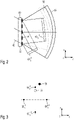
- the structure pattern 54 is configured in such a way that the input wave 42 is converted into a non-spherical output wave 56, a spherical output wave 58 and plane output waves 60 by diffraction at the structure pattern 54, as depicted in Figure 2 .
- the spherical output wave and the plane output waves 60 serve as calibration waves, as will be clarified below.
- the output wave 56 is also plotted in Figure 1 and serves as measurement wave for measuring the actual shape of the optical surface 12 of the optical element 14. To this end, the output wave 56 has a wavefront which is adapted to the intended shape of the optical surface 12. The output wave 56 is therefore also referred to as adapted measurement wave. As mentioned above, the output wave 56 is non-spherical and therefore has a rotationally symmetric aspherical wavefront or a wavefront in the form of a free-form surface. A free-form surface within the meaning of the application has no rotational symmetry, as already explained in the general part of the description.
- Figure 4 depicts the wave vector k i (in) of the input wave 42, the wave vector k i (S) of the spherical output wave 58 and the wave vector ki(A) of the non-spherical output wave 56 at a spatial coordinate i(x,y) on the diffractive structure pattern 54 in two sectional illustrations, once, in (a), in the yz-section and, in (b), in the xy-section.
- the diffractive structure pattern 54 is arranged in the xy-plane.
- angle ⁇ i The angle between the difference vector [k i (A)-k i (in)] and the difference vector [k i (S)-k i (in)] is referred to as angle ⁇ i .
- the angle ⁇ i xz plotted in (a), is the projection of ⁇ i in the xz-plane and the angle ⁇ i xy , plotted in (b), is the projection of ⁇ i in the xy-plane.
- angle ⁇ The mean value of the absolute value of the angle ⁇ i xy , i.e. of the angle ⁇ i projected into the xy-plane, over the spatial coordinates i(x,y) of the diffractive structure pattern 54 is referred to as angle ⁇ .
- the angle ⁇ is greater than 5°.
- 1 2 ⁇ i 1 N ⁇ xy k i A ⁇ k i in s i S ⁇ k i in > 5 ° .
- N denotes the number of points i, over which the mean value is formed.
- ⁇ is greater than 10° or greater than 15°.
- the structure pattern 54 in accordance with Figure 2 comprises a complex encoded phase grating f G , which contains various phase functions f 1 to f 4 such that respective diffracted waves are generated for each individual one of the various phase functions f 1 to f 4 .
- the illustrations depicted in Figure 5 show contour lines of the functions f 1 to f 4 . These contour lines of the phase functions correspond to the grating lines of the respective diffraction grating.
- the illustration of f G depicted in Figure 5 shows a greatly magnified section of the structure pattern 54 in accordance with Figure 2 .
- the complex encoded phase grating f G has such an effect on the input wave 42 that corresponding, mutually independent, diffracted waves of first diffraction order are generated by each of the diffraction gratings defined by the phase functions f 1 to f4.
- the strength of the individual contributions is set by the weights W1 to W4.
- the imaginary unit is i.
- a continuous phase grating is used for realizing the complex encoded phase grating f G .
- f G exp( i ⁇ ⁇ S ⁇ ).
- the diffraction efficiencies of the individual phase functions f 1 , f 2 , f 3 and f 4 have different magnitudes; in the present embodiment, the phase functions f 1 and f 2 are each included with a weight W 1 or W 2 of 35% and the phase functions f 3 and f 4 are each included with a weight W 3 or W 4 of 15%.
- phase function f 1 of the phase grating f G in accordance with Figure 5 generates the non-spherical output wave 56.
- phase function f 2 of the phase grating f G generates the spherical output wave 58.
- the grating periods corresponding to the phase functions f 1 and f 2 vary spatially over the diffractive structure pattern 54 in accordance with Figure 2 .
- phase functions f 3 and f 4 of the phase grating f G are linear gratings for generating plane waves (P), respectively in +1st and -1st order of diffraction.
- the phase function f 3 is configured as y-linear grating for generating plane output waves which are deflected in relation to the input wave 42 in the +/-y-direction.
- the plane output waves 60 y +1 and 60 y -1 plotted in Figure 2 , are waves which are generated by the y-linear grating in +1st and -1st order of diffraction.
- Figure 3 shows the output waves in the direction space generated by the center of the diffractive structure pattern 54 in accordance with Figure 2 .
- the x- and y-coordinates in the direction space are the x- and y-coordinates of the vector, normalized to one, in the propagation direction.
- the components of this direction vector are referred to as direction cosine. The following applies: -1 ⁇ x ⁇ 1, -1 ⁇ y ⁇ 1 and x 2 + y 2 ⁇ 1.
- the output waves 60 y +1 and 60 y -1 are offset in relation to the non-spherical output wave 56 in the +y - or -y - direction
- the output waves 60 x +1 and 60 x -1 are offset in relation to the non-spherical output wave 56 in the -y - and +x - or -x - direction.
- the output waves 60 x +1 and 60 x -1 are likewise plane waves and are generated by the phase function f 4 configured as x-linear grating in +1st and -1st order of diffraction.
- the propagation direction of the spherical output wave 58 is tilted in +x - and +y - direction compared to the propagation direction of the non-spherical output wave 56.
- the measurement system 10 Before measuring the optical element 14, during which the latter, as depicted in Figure 1 , is arranged in the beam path of the non-spherical output wave 56, the measurement system 10 is initially operated in a calibration mode. In this mode, a calibration sphere 62 is initially arranged instead of the optical element 14 on the output wave-side in respect of the diffractive optical element 50, and to be precise in the beam path of the spherical output wave 58, as illustrated in Figure 6 .
- the spherical output wave 58 is incident on the calibration sphere 62, the shape of which was determined previously in absolute terms.
- This absolute determination can, for example, be brought about by means of the shearing technique known to a person skilled in the art or by means of the likewise known three position test.
- the spherical output wave 58 After reflection at the calibration sphere 62, the spherical output wave 58 passes through the diffractive optical element 50 and is directed onto a detection area 47 of a camera chip 48 of the interferometer camera 45 by means of a lens system 46 of the interferometer camera 45. An interference pattern is generated on the detection area 47 by superposition with the reference wave 40, from which interference pattern the deviation of the spherical output wave 58 from its intended wavefront in the form of an ideal spherical wave is determined by means of an evaluation device 49. Hence, the actual wavefront of the output wave 58 is determined in absolute terms by means of the calibration sphere 62. The deviations of the spherical output wave 58 from its intended wavefront are stored as calibration deviations K1.
- the calibration sphere is thereupon removed again from the output wave-side beam path of the diffractive optical element 50 and, instead, a plane mirror 64 is successively arranged in the respective beam paths of the plane output waves 60 y +1 and 60 y -1 and 60 x +1 and 60 x -1 , as depicted in Figure 7 for the output wave 60 y +1 in (a) and for the output wave 60 y -1 in (b).
- the plane mirror 64 is in each case arranged such that the appropriate output wave 60 y +1 , 60 y -1 , 60 x +1 or 60 x -1 is reflected onto itself and returns to the interferometer 16 of the measurement system 10 after passing through the diffractive optical element 50 in the beam path of the input wave 42 and interferes with the reference wave 40 on the detection area 47 of the camera chip 48.
- the camera chip 48 records respective interference patterns for each of the two output waves 60 y +1 and 60 y -1 .
- the two output waves 60 y +1 and 60 y -1 are generated by diffraction in +1st and -1st order of diffraction at the y-linear grating formed by the phase function f 3 .
- the interference patterns recorded for the two output waves 60 y +1 and 60 y -1 are combined with one another in the evaluation device 49 such that, as a result, the x-coordinates of a distortion of the phase function f 3 are established over the whole area of the diffractive structure pattern 54 on the diffractive optical element 50.
- the difference between the two interference patterns is formed in this case.
- the interference patterns of the output waves 60 y +1 and 60 y -1 and the output waves 60 x +1 and 60 x -1 and the spherical output wave 58 can be combined with one another, for example by summing, in such a way that this can therefore be used to establish the shape or profile deviations of the substrate surface, having the diffractive structure pattern 54, of the diffractive optical element 50.
- the shape and profile deviations established thus are also stored as further calibration deviations K3.
- the optical surface 12 of the optical element 14 is measured by means of the measurement system 10.
- the test object in the form of the optical element 14 is, as shown in Figure 1 , arranged in the beam path of the non-spherical output wave 56 such that the latter is incident in autocollimation on the optical surface 12 and reflected thereon.
- the reflected wave thereupon returns through the diffractive optical element 50 as returning measurement wave 66 to the interferometer 16.
- the returning measurement wave 66 interferes with the reference wave 40 on the detection area 47 and thereby generates an interferogram.
- the interferogram is evaluated by means of the evaluation device 49 and this is used to establish the deviation of the actual shape of the optical surface 12 from the intended shape thereof. All calibration deviations established previously are taken into account during the evaluation.
- the method renders it possible to eliminate the substrate errors of the substrate 50 and the errors as a result of the distortion of the diffractive structure pattern 54. Furthermore, by means of the calibration deviations K3, the method renders it possible to reduce the errors in the shape or profile deviations of the diffractive structure pattern 54.
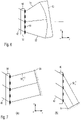
- Figures 8 to 12 depict a further embodiment of the diffractive optical element 50 for use in the measurement system 10 from Figure 1 .
- the diffractive structure pattern 54 of this diffractive optical element 50 is configured such that, by diffraction at the structure pattern 54, the input wave 42 is furthermore converted into three spherical output waves 70, 72 and 74 in addition to the non-spherical output wave 56 also generated by the diffractive structure pattern of Figure 2 .
- Figure 9 depicts the output waves 56, 70, 72 and 74 in the direction space. It is possible to gather from this illustration that the spherical output waves 70, 72 and 74 are arranged around the non-spherical output wave 56. Here, the direction vectors of the spherical output waves 70, 72 and 74 form a triangle. The direction vector of the non-spherical output wave 56 advantageously lies within the triangle.
- Figure 10 depicts the composition of the complex encoded phase grating f G of the structure pattern 54 in accordance with Figure 8 .
- the part of the phase grating f G displayed in Figure 10 is a greatly magnified section of the corresponding structure pattern 54. All that is depicted is a square section with an edge length of 50 ⁇ m.
- the diffractive optical element 50 in accordance with one embodiment is arranged on a square substrate 52 with an edge length of 500 mm.
- the diffractive structure pattern 54 is circular and largely covers the substrate 52.
- the complex encoded phase grating f G of the structure pattern 54 in accordance with Figure 8 contains the individual phase functions f 1 to f4.
- a separate output wave is generated for each individual phase function f 1 to f 4 by appropriate diffraction when the input wave 42 is radiated onto the diffractive optical element 50.
- the non-spherical output wave 56 is generated at the phase function f 1 .
- the non-spherical output wave 56 serves as measurement wave.
- the spherical output wave 70 is generated at the phase function f 2
- the spherical output wave 72 is generated at the phase function f 3
- the spherical output wave 74 is generated at the phase function f 4 .
- the phase function f 1 is weighted twice as strongly as the remaining phase functions f 2 to f 4 , the weight of which is 20% in each case.
- the three spherical output waves 70, 72, and 74 may also be referred to as calibration waves.
- Figure 11 firstly shows the diffraction efficiency E of the diffractive optical element 50 in accordance with Figure 8 during a single passage and secondly the contrast C during two passages through the diffractive optical element 50 of the interference pattern registered by the camera chip 48 of the interferometric measurement system, firstly for the non-spherical output wave 56 (FF) and secondly for the spherical output waves 70, 72 and 74 (SP1, SP2 and SP3).
- the corresponding diffraction efficiencies or contrasts are plotted depending on the weight of the phase function f 1 generating the non-spherical output wave 56 (FF).
- the diagrams relate to an embodiment in which the Fizeau element 36 reflects 0.4%, the optical surface 12 of the non-spherical area reflects 4% and the optical surfaces of calibration spheres adapted to the spherical output waves 70, 72 and 74 each reflect 80%. It becomes clear from the diagrams that in the case of the weight of f 1 in accordance with Figure 10 with 40%, this results in a diffraction efficiency in a single passage of slightly less than 25%, while the contrast is slightly over 90%. The contrast of the spherical output waves 70, 72 and 74 then lies at nearly 85%.
- the measurement system 10 when using the diffractive optical element 50 in accordance with Figure 8 is initially operated in the calibration mode.
- the calibration spheres adapted to the spherical output waves 70, 72 and 74 are successively arranged in a corresponding manner in the respective beam path of the output waves 70, 72 and 74 and measured by interferometry in each case.
- the interferometric measurement results are stored in the evaluation device 49 as calibration measurement data for each of the spherical output waves 70, 72 and 74.
- the measurement data obtained thereby are evaluated by the evaluation device 49 taking into account the stored calibration measurement data. Since the calibration measurement data obtained during the measurement of the spherical output waves 70, 72 and 74 are taken into account, manufacturing errors of the diffractive optical element 50 can be corrected in the measurement result of the optical surface 12, as a result of which the shape of the optical surface 12 can be determined with high accuracy. Manufacturing errors which can be corrected here include shape or profile deviations of the substrate surface, having the diffractive structure pattern 54, of the diffractive optical element 50 and distortion effects in the diffractive structure pattern 54.
- the diffraction grating formed by the diffractive structure pattern 54 in the embodiment in accordance with Figure 8 is configured such that a stripe density of the grating lines averaged within a square measurement area of the diffraction grating with 1 mm edge length over any square partial area with 50 ⁇ m edge length has a variation which extends over a span of less than 20 lines per millimeter.
- the diffractive structure pattern 54 which is arranged on the substrate 52 of the diffractive optical element 50 and, in accordance with one embodiment, has a circular form with a diameter of approximately 500 mm, is subdivided into individual square measurement areas MF, each with a side length of 1 mm.
- the measurement areas MF are in turn subdivided into individual square partial areas TF with a respective side length of 50 ⁇ m.
- a respective periodic distance d i is established at measurement points i along each grating line GL, which measurement points are in each case separated by 1 ⁇ m.
- the periodic distance d i results from the sum of the width of the grating line GL at the measurement point i and the width of the space to the next grating line adjoining on one side thereto.
- the measured periodic distances d i are converted into the stripe density values D i by forming an inverse.
- the values for the stripe density D i thus obtained are averaged over all measurement points i of all grating lines GL within the relevant partial area TF.
- a mean stripe density D M is determined for every partial area TF within the measurement area MF.
- the variation of the mean stripe densities D M for the individual partial areas TF has a span of less than 20 lines per millimeter.
- the mean stripe densities D M established for the various partial areas TF within the measurement area MF vary by less than 20 lines per millimeter.
- the stripe density D M on average is 200 lines per millimeter over all partial areas TF, the stripe density may, in accordance with the specification mentioned above, at most vary within the range of between 190 and 210 lines per millimeter.
- Figures 13 and 14 depict a further property of the diffractive structure pattern 54 in the embodiment in accordance with Figure 8 .
- Figure 13 shows a square section with 50 ⁇ m edge length of the diffraction grating formed by the diffractive structure pattern 54 and
- Figure 14 shows the section A from Figure 13 , in which one of the grating lines GL is contained.
- the diffraction grating depicted in Figure 13 has a mean periodic distance p, which is determined by a center-to-center distance between in each case neighboring grating lines GL, averaged over the diffraction grating. It is also possible to determine the mean periodic distance by averaging the established periodic distances d i , which were described above with reference to Figure 12 .
- the grating lines GL have a wave-like form, to be precise such that a mean wave period ⁇ of the grating lines lies in the region between 3 times and 20 times the mean periodic distance d of the diffraction grating. Furthermore, the grating lines GL have a variation over a span ⁇ transversely to their longitudinal extent, which lies in the region between 0.1 times and 3 times the mean periodic distance p of the diffraction grating.
- the span ⁇ can either be determined by virtue of the edge boundaries of the corresponding grating line GL being approximated by straight boundary lines 76 and the deviations of the grating line GL at the wave peak and in the wave trough being determined in relation to the corresponding approximated boundary line 76.
- the sum of these deviations i.e. the sum of the deviation ⁇ 1 at the wave peak and the deviation ⁇ 2 in the wave trough result in the span ⁇ of the variation.
- the span ⁇ can also be determined by virtue of a straight auxiliary line 78 being pushed toward the grating line from one side until said auxiliary line adjoins the grating line GL.
- the maximum distance between the edge boundary of the grating line GL and the auxiliary line 78 then likewise corresponds to the span ⁇ .
- Figures 15 and 16 show depictions of output waves in the direction space which are generated by further embodiments of the diffractive striped pattern 54.
- four further separate spherical output waves 70, 72, 74 and 80, serving as calibration waves are generated in addition to the centrally arranged non-spherical output wave 56, serving as measurement wave, by diffraction at the striped pattern 54 from the input wave 42.
- the spherical output waves 70, 72, 74 and 80 are arranged such that they do not lie symmetrically about the non-spherical output wave, i.e. the respective opposite "space", which is defined by mirroring the respective point on the non-spherical output wave 56 in the plane of the illustration in the direction space, remains free.
- the respective mean propagation directions of the spherical output waves 70, 72, 74 and 80 in pairs are in each case not arranged symmetrical to one another in relation to an axis defined by the mean propagation direction of the non-spherical output wave 56.
- the spherical output waves 80 and 70 are, in the plane of the illustration in the direction space, arranged symmetrically to the spherical output waves 72 and 74 in relation to the symmetry axis arranged transversely to the propagation direction of the non-spherical output wave 56.
- this symmetry is lacking, but the spherical output waves 70 and 74 as well as 72 and 76 are in each case arranged on a straight line extending through the non-spherical output wave 56 in the plane of the illustration in the direction space.
- the diffractive structure pattern 54 are embodied as multilevel phase gratings, as depicted in Figure 17 using the example of the phase pattern f G from Figure 10 .
- a multilevel phase grating should be understood to mean a phase grating which has at least one intermediate level between the uppermost and the lowermost level. Hence, such a phase grating has at least three levels; four levels are provided in the embodiment shown in Figure 17 .
- the use of multilevel phase gratings renders it possible, at least in part, to compensate or even to overcompensate for a diffraction efficiency loss brought about by the undertaken complex encoding.
- Figures 18 and 19 depict an embodiment of an optical element 14 in the form of a lens element or a mirror, in particular in the form of a mirror for an EUV projection exposure apparatus.
- the optical element 14 has an optical surface 12 formed as a free-form surface.
- the optical surface 12 of the optical element 14 was initially made to approximate a predetermined intended shape in the form of a free-form surface in accordance with the production accuracy.
- the approximated surface 12 was thereupon measured by means of the interferometric measurement system 10 using the diffractive optical element 50 in one of the embodiments and hence the deviation of said surface from the intended shape was determined with high accuracy.
- the surface 12 was processed further at suitable points on the basis of the measurement result such that said surface has the specifications specified below.
- Figure 18 shows the optical element 14 in a top view.
- the diameter d is approximately 600 mm.
- Figure 19 shows a schematic cross section of the optical element along an axis 80 of the optical element 14.
- the axis 80 is the rotational axis of a rotationally symmetric asphere 82 with the best fit to an intended shape 84 of the optical surface 12 and arranged in the z-direction in the drawing.
- the intended shape 84 has the form of a free-form surface and is therefore not rotationally symmetric.
- the deviations of the optical surface 12 from the intended shape 84 shown in Figure 19 are depicted with much magnification and in a schematic manner for illustration purposes.
- the maximum deviation ⁇ of the intended shape 84 from the rotationally symmetric asphere 82 with the best fit is approximately 6 ⁇ m in the present embodiment and hence is greater than 5 ⁇ m.
- the deviation of the actual shape of the optical surface 12 from the intended shape 84 is described by a 2-dimensional deviation D(x,y), where x and y denote the coordinates on the surface 12.
- the deviations in D(x,y), which trace back to oscillations with vibration wavelengths of between d/100, i.e. approximately 5 mm, and d/5, i.e. approximately 100 mm, are at most 0.05 nm.
- the function d(v) is obtained, where v denotes the frequency.
- the amplitudes of the function d(v) in the region between the frequencies which correspond to the boundary values of the vibration wavelength range specified above are therefore at most 0.05 nm.
Description
- The invention relates to a method for determining a deviation of an actual shape from an intended shape of an optical surface of an optical element.
- A device for determining a deviation of an actual shape from an intended shape is described in e.g.
US 2010/0177321 A1 . This device comprises an interferometer for generating a measurement wave, the wavefront of which is adapted to an aspherical intended shape of the optical surface by means of a diffraction grating. The wavefront of the adapted measurement wave is evaluated by interferometry after reflection at the optical surface and the deviation of the actual shape of the optical surface from the intended shape thereof is determined in the process. - In this case, the diffraction grating can for example be a computer-generated hologram (CGH), which is generated by virtue of the design of the interferometer being simulated by a suitable calculation method, such as e.g. a ray tracing method, and, in the process, a phase function of the diffraction grating being calculated such that the latter has a desired function in the beam path of the interferometer arrangement. It is then possible to produce the diffraction grating from the calculated phase function thereof.
- The accuracy of the shape measurement depends on the accuracy of the CGH.
- Here, it is not an exact-as-possible production which is decisive, but rather an exact-as-possible measurement of all possible errors in the CGH. Known errors can be removed by calculation when measuring the shape of the test object. Hence, the CGH forms the reference. While it is possible to calibrate all non-rotationally symmetric errors absolutely in the case of rotationally symmetric aspheres, all CGH errors have an impact on the shape measurement in the case of free-form surfaces, i.e. non-spherical surfaces without rotational symmetry. As a result, there is a sharp increase in the requirements in respect of the accuracy of the measurement of the CGH. In the process, it is important to know very precisely the distortion of the diffracting structures of the CGH, i.e. the lateral positions of the diffractive structures in relation to their intended positions, and the shape of the profile of the CGH. However, the measurement accuracy with which these parameters can be determined by means of measuring instruments known from the prior art does not suffice for the continuously increasing demands. Other known apparatuses for highly accurately measuring optical surfaces use two CGHs arranged in series, as a result of which the effort required for the measurement configuration increases.
- It is an object of the invention to solve the aforementioned problems and, in particular, to provide a method for measuring optical surfaces of any shape, in particular non-spherical optical surfaces without rotational symmetry, with an improved accuracy.
- The problem is solved according to the invention by the method of
claim 1. - According to a comparative example a diffractive optical element has a substrate and a diffractive structure pattern arranged on the substrate. The diffractive structure pattern is configured to convert a plane or spherical input wave radiated thereon into at least four separate output waves, wherein at least one of the output waves is a non-spherical wave, at least a further one of the output waves is a spherical wave and at least two further ones of the output waves respectively are a plane wave or a spherical wave.
- The aforementioned output waves are thus generated by means of merely a single diffractive optical element, i.e. a diffractive structure pattern which is arranged on a single substrate. Hence, the diffractive optical element can be configured in accordance with several variants. In accordance with a first variant, the wave radiated thereon is plane and the output waves comprise at least one non-spherical wave and at least three spherical waves. In accordance with a second variant, the wave radiated thereon is spherical and the output waves comprise at least one non-spherical wave and at least three spherical waves. In accordance with a third variant, the wave radiated thereon is plane and the output waves comprise at least one spherical wave and at least two plane waves. In accordance with a fourth variant, the wave radiated thereon is spherical and the output waves comprise at least one spherical wave and at least two plane waves. In the case of the first and the second variant, the intensities of the spherical waves differ by less than 30%, in particular by less than 10%, from one another in accordance with one embodiment.
- It is also possible to refer to the plane or spherical input wave as spherical wave only, with, in this case, a plane wave counting as a special case of a spherical wave with an infinite radius. The non-spherical output wave can be a measurement wave adapted to an optical surface to be measured, which measurement wave is radiated onto the surface when the latter is measured by interferometric means. The further output waves can also be referred to as calibration waves.
- The diffractive optical element is, in particular, embodied as computer-generated hologram (CGH). The diffractive structure pattern can also be referred to as phase grating or diffraction grating, although it should be noted that this should not necessarily be understood to mean a regular grating, but rather, in particular, line structures which can have bends, which can, in principle, deviate from one another in terms of their shape and which can have a variable distance between them. As explained above, the diffractive structure pattern is arranged on the substrate of the diffractive optical element, i.e. it is merely arranged on one substrate. The diffractive structure pattern is therefore not composed of several sub-patterns which are arranged on different substrates.
- A diffractive structure pattern which generates separate output waves as described above may be configured as a complex encoded phase grating. Within the meaning of the application, a spherical wave is a wave with a spherical wavefront, i.e. a wave in which the wavefront is formed by at least a spherical surface section.
- Within the meaning of the application, a non-spherical wave is a wave, the wavefront of which has a deviation of at least 10 λ from any ideal sphere, in particular from the sphere with the best fit to the wavefront, where λ is the wavelength of the input wave radiated thereon. In other words, the non-spherical wave has at least one point at which it deviates from every ideal sphere by at least 10 λ. If the wavelength is 500 nm, a non-spherical wave within the meaning of the application has a deviation of at least 5 µm from any ideal sphere. Within the meaning of the application, non-spherical waves comprise both waves with rotationally symmetric wavefronts, i.e. aspherical waves in the conventional sense, and waves with non-rotationally symmetric wavefronts, i.e. waves, the wavefronts of which have the shape of so-called free-form surfaces.
- In accordance with one embodiment, the non-spherical wave has a wavefront in the form of a free-form surface, wherein the wavefront has a deviation of at least 1 mm from any ideal sphere.
- Here, "separate output waves" should be understood to mean that the output waves have different propagation directions and can therefore be detected or reflected back to the diffractive optical element independently of one another, such that these can be measured separately in an interferometric measurement system.
- Compared to a CGH conventionally employed for interferometric measurements of the shape, the diffractive optical element according to the invention differs in that, according to the invention, at least three further output waves, which are plane or spherical, are generated in addition to the non-spherical output wave. In the aforementioned conventional CGH, no more than two plane or spherical waves are generated, in addition to one or more non-spherical waves, in the different orders of diffraction.
- If two CGHs, arranged in series, are used, a wave which is formed by a sphere and a non-sphere and which is therefore likewise non-spherical is usually radiated onto the second CGH. If a plane or spherical wave were to be radiated onto this CGH, not a single plane or spherical wave would be generated in the process.
- Generating the at least three further output waves of the aforementioned type in addition to the non-spherical output wave when a plane or spherical input wave is radiated onto the diffractive optical element according to the invention renders it possible for the diffractive optical element to be measured in respect of manufacturing errors by means of the further output waves. During a then subsequent measurement of an optical surface using the diffractive optical element, it is then once again possible to remove from the measurement result by calculation the effects of the manufacturing error. As a result, it is possible to increase the measurement accuracy of measuring the shape, in particular of non-spherical optical surfaces.
- In accordance with one embodiment, the structure pattern is configured such that the at least two further output waves are plane waves, the propagation directions of which are symmetrical to one another in relation to a direction of incidence of the input wave. In accordance with one variant, the two plane output waves are a positive and negative order of diffraction of the same order, such as e.g. the +1st and -1st order of diffraction, at a linear grating.
- In accordance with a further embodiment, the structure pattern is configured such that, in addition to the two plane output waves forming a first wave pair, the separate output waves have two further plane waves in the form of a second wave pair, the propagation directions of which are likewise symmetrical to one another in relation to the direction of incidence, with a plane spanned by the propagation directions of the first wave pair deviating from the plane spanned by the propagation directions of the second wave pair. In particular, the plane spanned by the propagation directions of the first wave pair is substantially perpendicular to the plane spanned by the propagation directions of the second wave pair. In this context, substantially perpendicular means an angle of at least 80°, in particular at least 85°, at least 89° or approximately 90°.
- In accordance with a further embodiment, an angle αi is defined at every point i of the diffractive structure pattern by the angle between a first difference vector and a second difference vector, the first difference vector being defined by the difference between the wave vector ki(A) of the non-spherical wave emanating from the point i and the wave vector ki(in) of the input wave impinging on the point i and the second difference vector being defined by the difference between the wave vector ki(S) of the at least one spherical wave emanating from the point i and the wave vector ki(in) of the input wave impinging on the point i. Furthermore, the structure pattern is configured such that the absolute value of the angle αi, averaged over the points i of the diffractive structure pattern, is greater than 5°, in particular greater than 10°, in projection onto a plane parallel to the structure pattern. The wave vector is also referred to as "k-vector" and is that vector which is perpendicular to the wavefront of a wave. In other words, an angle ω is greater than 5°, where ω is defined as follows:

- Here, N denotes the number of points i over which the mean value is formed. Expressed once again in other words, the angle ω is defined by the mean value of the absolute value of the angle αi xy over the spatial coordinates i of the diffractive optical element, i.e.

- Here, the mean is formed over the area covered by the structure pattern, i.e. the optically effective area of the diffractive optical element. The propagation direction of the input wave is referred to as the z-direction, and so the xy-plane is the plane perpendicular to the propagation direction of the input wave.
- In accordance with a further embodiment, the diffraction efficiency of the structure pattern for generating the non-spherical wave is at least 50% greater than the diffraction efficiency of the structure pattern for generating the at least one spherical wave. As a result, the intensity of the non-spherical wave is at least 50% greater than the intensity of the at least one spherical wave. In accordance with one embodiment variant, the diffraction efficiency for generating the at least one non-spherical wave is at least 70% greater, in particular at least 100% greater, than the diffraction efficiency for generating the at least one spherical wave. This can be compensated for by using metallized calibration mirrors. In accordance with one embodiment, the sum of the diffraction efficiencies of the at least four output waves is greater than 30%.
- In accordance with a further embodiment, the structure pattern is configured such that the radiation power of the non-spherical output wave is greater than the respective radiation power of the spherical or the plane output waves. That is to say, the output wave with the non-spherical wavefront is weighted more strongly in the structure pattern than the remaining three output waves with the spherical or the plane wavefront. In accordance with one exemplary embodiment, the radiation power of the output wave with the non-spherical wavefront has at least 30%, in particular approximately 40%, of the radiation power of the input wave and the remaining three output waves with the spherical or the plane wavefront each have between 15% and 25%, in particular approximately 20%, of the radiation power of the input wave.
- In accordance with a further embodiment, the structure pattern is configured such that the input wave radiated thereon is converted into at least five separate output waves, with four of the output waves being embodied as spherical waves. A further one of the at least five output waves is the non-spherical wave, in particular a free-form wave.
- In accordance with a further embodiment, the output waves have respective mean propagation directions which are oriented to one another such that the mean propagation directions of the four spherical output waves in pairs are in each case not arranged symmetrical to one another in relation to an axis defined by the mean propagation direction of the non-spherical output wave. In this context, "not symmetrical" is understood to mean that there is a deviation of at least 1°, in particular of at least 5°, compared to symmetric arrangement. The mean propagation direction is that propagation direction which emerges from intensity-weighted averaging of the different propagation directions of each output wave. In accordance with one embodiment variant, this condition applies to at least 90% of all points on the diffractive optical element.
- In accordance with a further embodiment, the diffractive structure pattern comprises a multilevel phase grating. As a person skilled in the art is well aware, a multilevel phase grating is understood to mean a phase grating which has at least one intermediate level between the uppermost and the lowermost level. Hence, such a phase grating has at least three levels. In accordance with different embodiments, provision can be made for four or more levels. A so-called blazed phase grating has so many levels that the profile is represented by inclined surfaces. The use of a multilevel phase grating renders it possible to at least partially compensate or even overcompensate for a loss in diffraction efficiency caused by complex encoding. Within the meaning of the application, a multilevel phase grating should also be understood to mean such a blazed phase grating. A person skilled in the art can obtain background information in respect of multilevel phase gratings from the handbook by Donald C. O'Shea et al. "Diffractive optics: design, fabrication, and test", 2004, The Society of Photo-Optical Instrumentation Engineers, pages 29 to 35. A multilevel phase grating within the meaning of the application is, in particular, also understood to mean a laterally blazed phase grating, such as described e.g. in the H. Kleemann et al., "Combination of blazed and laterally blazed structures", Diffractive Optics and Micro-Optics, OSA Technical Digest (Optical Society of America), paper DTuC7, 2004.
- According to a further comparative example, provision is furthermore made for a diffractive optical element which comprises a substrate and a diffraction grating arranged thereon. The diffraction grating has grating lines arranged at a distance from one another, a mean periodic distance of the diffraction grating being determined by a center-to-center distance, averaged over the diffraction grating, between in each case neighboring grating lines. The grating lines having a wave-like form such that a mean wave period of the grating lines lies in the region between 3 times and 20 times the mean periodic distance of the diffraction grating and a variation in the grating lines transversely to their longitudinal extent has a span which lies in the region between 0.1 times and 3 times the mean periodic distance of the diffraction grating.
- The mean periodic distance of the diffraction grating is measured in the transverse direction of the grating lines. A waved form of the grating lines is understood to mean that the grating lines deviate upward and downward, i.e. transversely to the longitudinal extent of the grating lines, in relation to a respective straight line. Here, the wave period can vary from deflection to deflection. Here, the span of the variation of the grating lines transversely to the longitudinal extent thereof should be understood to mean a span of the deviations of the respective grating line from its imagined straight shape, i.e. from the straight line with the best fit to the respective grating line. In particular, the span of the variation is twice the amplitude of a wave determining the grating line shape.
- In accordance with a further embodiment, the diffraction grating covers at least 20% of the substrate. If the substrate has a plate- shaped design, 20% of the upper side and lower side, respectively, of the substrate are covered by the diffraction grating.
- In accordance with a further embodiment, at least 90%, in particular at least 95% or at least 99%, of the grating lines of the diffraction grating are embodied as continuous lines which extend without interruption between edge regions of the diffraction grating, i.e. these lines do not end within the area of the substrate covered by the diffraction grating.
- In accordance with a further embodiment, the diffraction grating is configured such that a stripe density of the grating lines averaged within a square measurement area of the diffraction grating with 1 mm edge length over any square partial area with 50 µm edge length has a variation which extends over a span of less than 20 line pairs/mm. In accordance with one example for a method for determining the stripe density within a square partial area, the sum of the width of the grating line and the width of the intermediate space, adjoining on one side, to the next grating line is initially determined every 1 µm along each grating line. The inverse of the value determined thereby is formed and hence the stripe density is established at the relevant measurement point. The values for the stripe densities are averaged over all measurement points within the relevant partial area. This happens for all partial areas within the square measurement area, i.e. for 20 x 20 = 400 partial areas, such that a mean stripe density is determined for each partial area. In accordance with the exemplary embodiment discussed above, the variation of the mean stripe density has a span of less than 20 line pairs/mm, i.e. the mean stripe densities established for the various partial areas within the measurement area vary by less than 20 line pairs/mm. By way of example, if the stripe density on average is approximately 200 lines/mm, the stripe density varies within the span of 190 to 210 lines/mm.
- In accordance with a further embodiment, the structure pattern is configured such that, in addition to the at least four separate output waves, a reference wave in Littrow reflection is also generated as reference wave from the input wave radiated thereon, which reference wave can be used as a reference during an interferometric measurement.
- The features described in the aforementioned embodiments and embodiment variants can be transferred individually or in combination to the diffractive optical element with the wave-like grating lines.
- Furthermore, according to another comparative example, provision is made for a diffractive optical element which has a substrate and a diffractive structure pattern arranged thereon. The diffractive structure pattern is configured such that the structure pattern converts a plane or spherical input wave radiated thereon into at least three separate output waves with in each case a spherical wavefront.
- The features described in the aforementioned embodiments and embodiment variants can be transferred individually or in combination to this diffractive optical element with the wave-like grating lines. In particular, this diffractive optical element can contain features from above-described embodiments of the diffractive optical element generating at least four separate output waves.
- According to the invention, a method for determining a deviation of an actual shape from an intended shape of an optical surface of an optical element is provided. This method comprises the following steps: generating an input wave, arranging a diffractive optical element in the beam path of the input wave and converting the input wave into at least three separate output waves by interaction with the diffractive optical element, wherein one of the output waves is a measurement wave, adapted to the intended shape of the optical surface, with a non-spherical wavefront, and at least two further ones of the output waves are calibration waves. The method further comprises the steps of determining calibration corrections of the diffractive optical element by means of each one of the at least two calibration waves, arranging the optical surface in the beam path of the adapted wave and measuring the wavefront of the adapted measurement wave after interaction with the optical surface, wherein the wavefront of the adapted measurement wave is measured with the diffractive optical element being oriented in respect of the input wave the same as during the determining of the calibration corrections. Further, according to the above method the measured wavefront is corrected by means of the determined calibration corrections.
- In different words, according to the above method the diffractive optical element is arranged in respect of the propagation direction of the input wave in a given orientation for determining the calibration corrections, wherein the calibration corrections are determined by analyzing each one of the at least two calibration waves. This orientation is unchanged when measuring the wavefront of the adapted wave. Again in different words, the input wave has the same direction of incidence in the local coordinate system of the diffractive optical element when generating and analyzing the measurement wave and when generating and analyzing the calibration waves. The output waves are especially generated simultaneously by interaction of the input wave with the diffractive optical element.
- As mentioned above, "separate output waves" is to be understood to mean that the output waves have different propagation directions and can therefore be detected or reflected back to the diffractive optical element independently of one another, such that these can be measured separately in an interferometric measurement system.
- By measuring the wavefront of the adapted wave with the diffractive optical element being oriented in respect of the input wave the same as during the determining of the calibration corrections allows an especially precise calibration of the diffractive optical element in respect of manufacturing errors, as the determined calibration corrections can be applied directly to the measured wavefront of the adapted wave. As the orientation remains unchanged, the determined calibration corrections precisely reflect the manufacturing errors of the diffractive optical element relevant to the generation of the measurement wave. In different words, no errors are introduced into the correction of the wavefront due to a deviation between the measured calibration corrections and the real deviations of the structure on the diffractive optical element generating the measurement wave, which deviation would be due to a different orientation of the diffractive optical element.
- According to an embodiment the wavefront of the adapted measurement wave is measured with the diffractive optical element being arranged in the same position in respect of the input wave as during the determining of the calibration corrections. That means both the orientation and the position of the diffractive optical element remains unchanged when measuring the wavefront of the adapted measurement wave.
- The at least two calibration waves include a first calibration wave and a second calibration wave. The calibration corrections of the diffractive optical element are determined by means of the first calibration wave and by means of the second calibration wave.
- According to a further embodiment the determining of calibration corrections includes determining first calibration corrections from a first one of the calibration waves and second calibration corrections from a second one of the calibration waves, wherein the first calibration corrections and the second calibration corrections are determined with the diffractive optical element being oriented the same in respect of the input wave, i.e. the orientation of the diffractive optical element is unchanged between determining the first calibration corrections and the second calibration corrections.
- According to a further embodiment, the diffractive optical element comprises a complex encoded phase grating. Such a complex encoded phase grating is configured with at least three phase functions f1 to f3 such that respective diffracted waves are generated for each individual one of the various phase functions f1 to f3, which diffracted waves form the above mentioned output waves. The diffracted waves generated for each of the phase functions f1 to f3 are each waves generated in the first diffraction order at the phase grating fG. The properties of a complex encoded phase grating according to the application is decribed in more detail in the subsequent detailed description of exemplary embodiments. The use of a complex encoded phase grating allows to configure the diffractive optical element such that the output waves have different intensities. This may be done by assigning different weights to the individual phase functions f1 to f3 within the complex encoded phase grating.
- According to an embodiment each one of the at least three output waves are generated in the same diffraction order at the diffractive optical element. Especially each one of the at least three output waves are generated in first diffraction order, in particular +1st diffraction order, at the diffractive optical element. In case of a complex encoded grating as described in this application only +1st diffraction order waves form the output waves. When generating the output waves in the first diffraction order, calibration waves having a simple geometrical shape, such as a plane or a spherical shape, can be generated. With such simple geometrical shapes a precise calibration can be accomplished, as appropriate calibration objects can be manufactured with high precision.
- According to a further embodiment the output waves have respective mean propagation directions which are oriented to one another such that the mean propagation directions of the at least two calibration waves are arranged asymmetrically, i.e. are not arranged symmetrical, to one another in relation to an axis defined by the mean propagation direction of the measurement wave. With such an asymmetric arrangement the generation of interfering or spurious light at the location of the measurement wave can be avoided.
- According to a further embodiment at least one of the calibration waves is a spherical wave. According to further embodiments of the invention at least two or at least three calibration waves are spherical waves.
- According to an embodiment of the invention the input wave is a plane or spherical wave, the input wave is converted into at least four separate output waves by interaction with the diffractive optical element, wherein at least one further one of the output waves is a calibration wave with spherical wavefront and at least two further ones of the output waves are calibration waves with, in each case, a plane or a spherical wavefront. The calibration corrections of the diffractive optical element are determined by means of the three calibration waves.
- The features mentioned above or below with regard to the method in any of the described embodiments according to the invention may be transferred to the diffractive optical element in any one of the described embodiments, especially to the diffractive optical element configured to convert an input wave into at least four separate output waves, and vice versa. Especially the diffractive optical element may be configured to generate the four separate output waves such that a wavefront of the non-spherical wave after interaction with an optical surface may be measured with the diffractive optical element being oriented in respect of the input wave the same as during a determining of calibration corrections by means of the other output waves. According to a further embodiment the diffractive optical element is configured to generate the four separate output waves simultaneously, especially such to generate each one of the output waves in first diffraction order.
- According to a further comparative example, provision is made for a method for determining a deviation of an actual shape from an intended shape of an optical surface of an optical element. In one embodiment, the method according to the invention comprises the following steps: generating a plane or spherical input wave, arranging a diffractive optical element in the beam path of the input wave and converting the input wave into at least four separate output waves by interaction with the diffractive optical element, wherein at least one of the output waves is a measurement wave, adapted to the intended shape of the optical surface, with a non-spherical wavefront, at least one further one of the output waves is a calibration wave with spherical wavefront and at least two further ones of the output waves are calibration waves with, in each case, a plane or a spherical wavefront. Furthermore, in accordance with the method according to the comparative example, calibration corrections of the diffractive optical element are determined by means of the calibration waves, the optical surface is measured in the beam path of the adapted measurement wave and the wavefront of the adapted measurement wave is measured after interaction with the optical surface. Furthermore, the measured wavefront is corrected by means of the determined calibration corrections. It is now possible to determine the deviation of the actual shape of the optical surface from the intended shape by means of the corrected wavefront.
- The diffractive optical element used in the method according to the invention can, in particular, be embodied in accordance with one of the above-described embodiments of the comparative examples. In accordance with one embodiment according to the invention, in order to determine the calibration corrections, one or more calibration objects are arranged in the beam paths of the calibration waves and there is an interferometric evaluation of the calibration waves after interaction with the calibration object or objects.
- Furthermore, according to a further comparative example, provision is made for a method for producing an optical element. In one embodiment, this method comprises the step of manufacturing the optical element with an optical surface which has a diameter of greater than 500 mm. Furthermore, an actual shape of the optical surface is measured so accurately in relation to an intended shape by interferometry using merely one diffractive optical element that deviations of the actual shape from the intended shape, which trace back to oscillations with vibration wavelengths of between d/100 and d/5, are determined with an accuracy of 0.05 nm, the intended shape being a free-form surface, which has a deviation from each rotationally symmetric asphere of more than 5 µm. Furthermore, the optical surface is adapted to the intended shape by mechanical processing of the optical surface on the basis of the interferometric measurement result. Adapting the optical surface to the intended shape in this case occurs within the scope of the measurement accuracy of the interferometric measurement.
- The interferometric measurement of the actual shape of the optical surface can, in particular, take place by carrying out the above-described measuring method in one of the embodiments according to the invention. The diffractive optical element used in the production method can, in particular, be embodied in one of the above-described embodiments.
- Furthermore, according to a further comparative example , provision is made for an optical element, which has an optical surface with a diameter d of greater than 500 mm. Here, an actual shape of the optical surface is adapted to an intended shape such that deviations of the actual shape from the intended shape, which trace back to oscillations with vibration wavelengths of between d/100 and d/5, are no more than 0.05 nm, in particular no more than 0.02 nm. Here, the intended shape is a free-form surface, which has a deviation from each rotationally symmetric asphere of more than 5 µm, in particular of more than 10 µm.
- By way of example, the optical element can be embodied as EUV mirror. In particular, the deviation of the intended shape from the rotationally symmetric asphere with the best fit thereto is more than 5 µm, in particular more than 10 µm. In accordance with exemplary embodiments, the optical surface can have a diameter of more than 1000 mm and all oscillations can relate to vibration wavelengths of between 1 mm and 50 mm.
- In accordance with a further embodiment, the intended shape has a deviation from every sphere of at least 1 mm. As a result, the optical surface is a large or strong free-form surface.
- In accordance with a further exemplary embodiment, deviations of the actual shape from the intended shape, which trace back to oscillations of between d/100 and d/5, are defined by the largest amplitude of the deviations of the actual shape from the intended shape at any point on the optical surface.
- Both the features mentioned above and other features of the embodiments according to the invention are explained in the claims and in the description of the figures, whereby the full scope of the present invention is only defined by the appended claims.
- The above and further advantageous features of the disclosure are illustrated in the following detailed description of exemplary embodiments with reference to the accompanying schematic drawings, in which:
- Figure 1
- shows a sectional view of an interferometric measurement system with a diffractive optical element,
- Figure 2
- depicts, in the sectional view in accordance with
Figure 1 , output waves generated by diffracting an input wave at the diffractive optical element in a first embodiment, - Figure 3
- depicts the output waves from
Figure 2 in the direction space, - Figure 4
- depicts angular relationships of wave vectors of two of the output waves in accordance with
Figure 2 , - Figure 5
- depicts the composition of a diffractive structure pattern of the diffractive optical element in accordance with
Figure 2 , - Figure 6
- depicts a calibration of the diffractive optical element by means of one of the output waves with a spherical wavefront,
- Figure 7
- depicts a further calibration of the diffractive optical element by means of plane output waves,
- Figure 8
- depicts, in the sectional view in accordance with
Figure 1 , output waves generated by diffracting the input wave at a further embodiment of the diffractive optical element, - Figure 9
- depicts the output waves from
Figure 8 in the direction space, - Figure 10
- depicts the composition of a diffractive structure pattern of the diffractive optical element in accordance with
Figure 8 , - Figure 11
- shows diagrams which depict diffraction efficiency and contrast when using the diffractive optical element in accordance with
Figure 9 in the interferometric measurement system in accordance withFigure 1 , - Figure 12
- depicts the size ratios of a section of the phase grating of the diffractive optical element in accordance with
Figure 8 in relation to the diffractive optical element as a whole, - Figure 13
- depicts a waviness of the grating lines of the phase grating from
Figure 8 , - Figure 14
- shows one of the grating lines from the phase grating of
Figure 13 , - Figure 15
- depicts output waves generated by means of diffraction at a further embodiment of the diffractive optical element, in the direction space,
- Figure 16
- depicts output waves generated by means of diffraction at a further embodiment of the diffractive optical element, in the direction space,
- Figure 17
- depicts a diffractive structure pattern, embodied as multilevel phase grating, of the diffractive optical element,
- Figure 18
- shows a top view of an optical element produced according to an example,and
- Figure 19
- shows a sectional view of the optical element from
Figure 18 . - In the exemplary embodiments or embodiments described below, elements which are functionally or structurally similar to one another are as far as possible provided with the same or similar reference signs. Therefore, for understanding the features of the individual elements of a specific exemplary embodiment, reference should be made to the description of other exemplary embodiments or the general description of the invention.
- To facilitate the description, a Cartesian xyz-coordinate system is indicated in the drawing, which system reveals the respective positional relationship of the components illustrated in the figures. In
Figure 1 , the x-direction extends perpendicularly to the plane of the drawing and into the latter, the y-direction extends upward and the z-direction extends toward the right. -
Figure 1 depicts aninterferometric measurement system 10 in one embodiment according to the invention. Themeasurement system 10 is suitable for determining a deviation of an actual shape from a non-spherical intended shape of anoptical surface 12 of a test object in the form of anoptical element 14. By way of example, theoptical element 14 can be embodied in the form of an optical lens element or of a mirror. In the illustrated case, theoptical element 14 is a concave mirror for the EUV lithography, i.e. a mirror which, in a microlithographic projection exposure apparatus, is designed with an exposure wavelength in the EUV wavelength range. The EUV wavelength range extends to wavelengths below 100 nm and relates, in particular, to wavelengths of approximately 13.5 nm and/or approximately 6.8 nm. Theoptical element 14 is assembled in themeasurement system 10 by means of a holder not depicted in the drawing. The non-spherical intended shape of theoptical surface 12 can have the shape of a rotationally symmetric asphere or a free-form surface, as described in more detail in the general description. - The
interferometric measurement system 10 comprises aninterferometer 16, which in turn comprises alight source 18, abeam splitter 34 and aninterferometer camera 45. Thelight source 18 generatesillumination radiation 20 and, to this end, it comprises alaser 21, such as a helium neon laser, for generating alaser beam 22. Theillumination radiation 20 has sufficiently coherent light for carrying out an interferometric measurement. In the case of a helium neon laser, the wavelength of theillumination radiation 20 is approximately 633 nm. However, the wavelength of theillumination radiation 20 can also have different wavelengths in the visible and non-visible wavelength range of electromagnetic radiation. - The
laser beam 22 is focused onto astop 26 by a focusinglens element 24 in such a way that a divergent beam of coherent light emanates from the aperture. The wavefront of thedivergent beam 28 is substantially spherical. Thedivergent beam 28 is collimated by a lens-element group 30, as a result of which theillumination radiation 20 is generated by a substantially plane wavefront in the present case. Theillumination radiation 20 propagates along anoptical axis 32 of theinterferometer 16 and passes through thebeam splitter 34. - The
illumination radiation 20 is thereupon incident on aFizeau element 36 with aFizeau area 38. A part of the light of theillumination radiation 20 is reflected at theFizeau area 38 asreference wave 40. The light of theillumination radiation 20 passing through theFizeau element 36 propagates as aninput wave 42, with aplane wavefront 44 along theoptical axis 32 and is incident on a diffractiveoptical element 50. In other embodiments of themeasurement system 10, the wavefront of theinput wave 42 can also be spherical. - In relation to the wavelength of the
illumination radiation 20, the diffractiveoptical element 50 comprises atransmissive substrate 52 and, arranged on thesubstrate 52, adiffractive structure pattern 54 in the form of a computer-generated hologram (CGH). - In a first embodiment, the
structure pattern 54 is configured in such a way that theinput wave 42 is converted into anon-spherical output wave 56, aspherical output wave 58 and plane output waves 60 by diffraction at thestructure pattern 54, as depicted inFigure 2 . The spherical output wave and the plane output waves 60 serve as calibration waves, as will be clarified below. - The
output wave 56 is also plotted inFigure 1 and serves as measurement wave for measuring the actual shape of theoptical surface 12 of theoptical element 14. To this end, theoutput wave 56 has a wavefront which is adapted to the intended shape of theoptical surface 12. Theoutput wave 56 is therefore also referred to as adapted measurement wave. As mentioned above, theoutput wave 56 is non-spherical and therefore has a rotationally symmetric aspherical wavefront or a wavefront in the form of a free-form surface. A free-form surface within the meaning of the application has no rotational symmetry, as already explained in the general part of the description. -
Figure 4 depicts the wave vector ki(in) of theinput wave 42, the wave vector ki(S) of thespherical output wave 58 and the wave vector ki(A) of thenon-spherical output wave 56 at a spatial coordinate i(x,y) on thediffractive structure pattern 54 in two sectional illustrations, once, in (a), in the yz-section and, in (b), in the xy-section. Here, thediffractive structure pattern 54 is arranged in the xy-plane. The angle between the difference vector [ki(A)-ki(in)] and the difference vector [ki(S)-ki(in)] is referred to as angle αi. The angle αi xz, plotted in (a), is the projection of αi in the xz-plane and the angle αi xy, plotted in (b), is the projection of αi in the xy-plane. - The mean value of the absolute value of the angle αi xy, i.e. of the angle αi projected into the xy-plane, over the spatial coordinates i(x,y) of the
diffractive structure pattern 54 is referred to as angle ω. In accordance with one embodiment, the angle ω is greater than 5°. Hence, the following applies:
- Here, N denotes the number of points i, over which the mean value is formed. In accordance with further embodiments, ω is greater than 10° or greater than 15°.
- As depicted in
figure 5 , thestructure pattern 54 in accordance withFigure 2 comprises a complex encoded phase grating fG, which contains various phase functions f1 to f4 such that respective diffracted waves are generated for each individual one of the various phase functions f1 to f4. The illustrations depicted inFigure 5 show contour lines of the functions f1 to f4. These contour lines of the phase functions correspond to the grating lines of the respective diffraction grating. The illustration of fG depicted inFigure 5 shows a greatly magnified section of thestructure pattern 54 in accordance withFigure 2 . In other words, the complex encoded phase grating fG has such an effect on theinput wave 42 that corresponding, mutually independent, diffracted waves of first diffraction order are generated by each of the diffraction gratings defined by the phase functions f1 to f4. One can imagine the complex encoded phase grating fG to be several CGHs with the individual phase functions f1 to f4 superposed at one point. This superposition of the functionalities corresponds to the operation S = W1 * exp(i*f1) + W2 * exp(i*f2) + W3 * exp(i*f3) + W4 * exp(i*f4). The strength of the individual contributions is set by the weights W1 to W4. The imaginary unit is i. In accordance with one embodiment according to the invention, a binary phase grating, i.e. fG = 0 or π, is used for realizing the complex encoded phase grating fc. - The following applies to the binary phase grating: if Re{S} > 0 then fG = π, else fG = 0. In accordance with a further embodiment according to the invention, a continuous phase grating is used for realizing the complex encoded phase grating fG. The following applies in this case: fG = exp(i∠{S}). The diffraction efficiencies of the individual phase functions f1, f2, f3 and f4 have different magnitudes; in the present embodiment, the phase functions f1 and f2 are each included with a weight W1 or W2 of 35% and the phase functions f3 and f4 are each included with a weight W3 or W4 of 15%.
- The phase function f1 of the phase grating fG in accordance with
Figure 5 generates thenon-spherical output wave 56. The phase function f2 of the phase grating fG generates thespherical output wave 58. The grating periods corresponding to the phase functions f1 and f2 vary spatially over thediffractive structure pattern 54 in accordance withFigure 2 . - The further phase functions f3 and f4 of the phase grating fG are linear gratings for generating plane waves (P), respectively in +1st and -1st order of diffraction. Thus, the phase function f3 is configured as y-linear grating for generating plane output waves which are deflected in relation to the
input wave 42 in the +/-y-direction. The plane output waves 60y +1 and 60y -1, plotted inFigure 2 , are waves which are generated by the y-linear grating in +1st and -1st order of diffraction. The plane output waves 60x +1 and 60x -1, generated by the x-linear grating which is formed by the phase function f4, cannot be seen inFigure 2 due to the sectional plane selected therein, but are depicted inFigure 3 instead. -
Figure 3 shows the output waves in the direction space generated by the center of thediffractive structure pattern 54 in accordance withFigure 2 . The x- and y-coordinates in the direction space are the x- and y-coordinates of the vector, normalized to one, in the propagation direction. The components of this direction vector are referred to as direction cosine. The following applies: -1 ≤ x ≤ 1, -1 ≤ y ≤ 1 and x2 + y2 ≤ 1. - While the output waves 60y +1 and 60y -1 are offset in relation to the
non-spherical output wave 56 in the +y - or -y - direction, the output waves 60x +1 and 60x -1 are offset in relation to thenon-spherical output wave 56 in the -y - and +x - or -x - direction. The output waves 60x +1 and 60x -1 are likewise plane waves and are generated by the phase function f4 configured as x-linear grating in +1st and -1st order of diffraction. In the shown embodiment, the propagation direction of thespherical output wave 58 is tilted in +x - and +y - direction compared to the propagation direction of thenon-spherical output wave 56. - Before measuring the
optical element 14, during which the latter, as depicted inFigure 1 , is arranged in the beam path of thenon-spherical output wave 56, themeasurement system 10 is initially operated in a calibration mode. In this mode, acalibration sphere 62 is initially arranged instead of theoptical element 14 on the output wave-side in respect of the diffractiveoptical element 50, and to be precise in the beam path of thespherical output wave 58, as illustrated inFigure 6 . - The
spherical output wave 58 is incident on thecalibration sphere 62, the shape of which was determined previously in absolute terms. This absolute determination can, for example, be brought about by means of the shearing technique known to a person skilled in the art or by means of the likewise known three position test. - After reflection at the
calibration sphere 62, thespherical output wave 58 passes through the diffractiveoptical element 50 and is directed onto adetection area 47 of acamera chip 48 of theinterferometer camera 45 by means of a lens system 46 of theinterferometer camera 45. An interference pattern is generated on thedetection area 47 by superposition with thereference wave 40, from which interference pattern the deviation of thespherical output wave 58 from its intended wavefront in the form of an ideal spherical wave is determined by means of anevaluation device 49. Hence, the actual wavefront of theoutput wave 58 is determined in absolute terms by means of thecalibration sphere 62. The deviations of thespherical output wave 58 from its intended wavefront are stored as calibration deviations K1. - The calibration sphere is thereupon removed again from the output wave-side beam path of the diffractive
optical element 50 and, instead, aplane mirror 64 is successively arranged in the respective beam paths of the plane output waves 60y +1 and 60y -1 and 60x +1 and 60x -1, as depicted inFigure 7 for theoutput wave 60y +1 in (a) and for theoutput wave 60y -1 in (b). Theplane mirror 64 is in each case arranged such that theappropriate output wave interferometer 16 of themeasurement system 10 after passing through the diffractiveoptical element 50 in the beam path of theinput wave 42 and interferes with thereference wave 40 on thedetection area 47 of thecamera chip 48. - The
camera chip 48 records respective interference patterns for each of the twooutput waves output waves output waves evaluation device 49 such that, as a result, the x-coordinates of a distortion of the phase function f3 are established over the whole area of thediffractive structure pattern 54 on the diffractiveoptical element 50. In accordance with one embodiment, the difference between the two interference patterns is formed in this case. - The same evaluation occurs for the two
output waves diffractive structure pattern 54 are established on the diffractiveoptical element 50. The distortion in x- and y-coordinates of the wholediffractive structure pattern 54 is thereupon deduced from the distortion coordinates thus obtained. This distortion vector field is stored as further calibration deviations K2 and serves for correcting thespherical output wave 58 and thenon-spherical output wave 56. - Furthermore, the interference patterns of the output waves 60y +1 and 60y -1 and the output waves 60x +1 and 60x -1 and the
spherical output wave 58 can be combined with one another, for example by summing, in such a way that this can therefore be used to establish the shape or profile deviations of the substrate surface, having thediffractive structure pattern 54, of the diffractiveoptical element 50. The shape and profile deviations established thus are also stored as further calibration deviations K3. - Finally, the
optical surface 12 of theoptical element 14 is measured by means of themeasurement system 10. To this end, the test object in the form of theoptical element 14 is, as shown inFigure 1 , arranged in the beam path of thenon-spherical output wave 56 such that the latter is incident in autocollimation on theoptical surface 12 and reflected thereon. The reflected wave thereupon returns through the diffractiveoptical element 50 as returningmeasurement wave 66 to theinterferometer 16. The returningmeasurement wave 66 interferes with thereference wave 40 on thedetection area 47 and thereby generates an interferogram. The interferogram is evaluated by means of theevaluation device 49 and this is used to establish the deviation of the actual shape of theoptical surface 12 from the intended shape thereof. All calibration deviations established previously are taken into account during the evaluation. - By means of the calibration deviations K1 and K2, the method renders it possible to eliminate the substrate errors of the
substrate 50 and the errors as a result of the distortion of thediffractive structure pattern 54. Furthermore, by means of the calibration deviations K3, the method renders it possible to reduce the errors in the shape or profile deviations of thediffractive structure pattern 54. -
Figures 8 to 12 depict a further embodiment of the diffractiveoptical element 50 for use in themeasurement system 10 fromFigure 1 . As depicted inFigure 8 , thediffractive structure pattern 54 of this diffractiveoptical element 50 is configured such that, by diffraction at thestructure pattern 54, theinput wave 42 is furthermore converted into three spherical output waves 70, 72 and 74 in addition to thenon-spherical output wave 56 also generated by the diffractive structure pattern ofFigure 2 . -
Figure 9 depicts the output waves 56, 70, 72 and 74 in the direction space. It is possible to gather from this illustration that the spherical output waves 70, 72 and 74 are arranged around thenon-spherical output wave 56. Here, the direction vectors of the spherical output waves 70, 72 and 74 form a triangle. The direction vector of thenon-spherical output wave 56 advantageously lies within the triangle. -
Figure 10 depicts the composition of the complex encoded phase grating fG of thestructure pattern 54 in accordance withFigure 8 . Like inFigure 5 , the part of the phase grating fG displayed inFigure 10 is a greatly magnified section of thecorresponding structure pattern 54. All that is depicted is a square section with an edge length of 50 µm. As depicted inFigure 12 , the diffractiveoptical element 50 in accordance with one embodiment is arranged on asquare substrate 52 with an edge length of 500 mm. In this embodiment, thediffractive structure pattern 54 is circular and largely covers thesubstrate 52. - As shown in
Figure 10 , the complex encoded phase grating fG of thestructure pattern 54 in accordance withFigure 8 contains the individual phase functions f1 to f4. A separate output wave is generated for each individual phase function f1 to f4 by appropriate diffraction when theinput wave 42 is radiated onto the diffractiveoptical element 50. - The
non-spherical output wave 56, the wavefront of which is adapted to the intended shape of theoptical surface 12 of theoptical element 14 to be measured, is generated at the phase function f1. Thenon-spherical output wave 56 serves as measurement wave. Thespherical output wave 70 is generated at the phase function f2, thespherical output wave 72 is generated at the phase function f3 and thespherical output wave 74 is generated at the phase function f4. With a 40% weight, the phase function f1 is weighted twice as strongly as the remaining phase functions f2 to f4, the weight of which is 20% in each case. The three spherical output waves 70, 72, and 74 may also be referred to as calibration waves. - In appropriate diagrams,
Figure 11 firstly shows the diffraction efficiency E of the diffractiveoptical element 50 in accordance withFigure 8 during a single passage and secondly the contrast C during two passages through the diffractiveoptical element 50 of the interference pattern registered by thecamera chip 48 of the interferometric measurement system, firstly for the non-spherical output wave 56 (FF) and secondly for the spherical output waves 70, 72 and 74 (SP1, SP2 and SP3). In the diagrams, the corresponding diffraction efficiencies or contrasts are plotted depending on the weight of the phase function f1 generating the non-spherical output wave 56 (FF). The diagrams relate to an embodiment in which theFizeau element 36 reflects 0.4%, theoptical surface 12 of the non-spherical area reflects 4% and the optical surfaces of calibration spheres adapted to the spherical output waves 70, 72 and 74 each reflect 80%. It becomes clear from the diagrams that in the case of the weight of f1 in accordance withFigure 10 with 40%, this results in a diffraction efficiency in a single passage of slightly less than 25%, while the contrast is slightly over 90%. The contrast of the spherical output waves 70, 72 and 74 then lies at nearly 85%. - Analogous to the measurement of the
optical surface 12 of theoptical element 14 by means of the diffractiveoptical element 50 in accordance withFigure 2 , themeasurement system 10 when using the diffractiveoptical element 50 in accordance withFigure 8 is initially operated in the calibration mode. To this end, the calibration spheres adapted to the spherical output waves 70, 72 and 74 are successively arranged in a corresponding manner in the respective beam path of the output waves 70, 72 and 74 and measured by interferometry in each case. The interferometric measurement results are stored in theevaluation device 49 as calibration measurement data for each of the spherical output waves 70, 72 and 74. - In the subsequent measurement of the
optical surface 12 of the test object in form of theoptical element 14 by means of thenon-spherical output wave 56, the measurement data obtained thereby are evaluated by theevaluation device 49 taking into account the stored calibration measurement data. Since the calibration measurement data obtained during the measurement of the spherical output waves 70, 72 and 74 are taken into account, manufacturing errors of the diffractiveoptical element 50 can be corrected in the measurement result of theoptical surface 12, as a result of which the shape of theoptical surface 12 can be determined with high accuracy. Manufacturing errors which can be corrected here include shape or profile deviations of the substrate surface, having thediffractive structure pattern 54, of the diffractiveoptical element 50 and distortion effects in thediffractive structure pattern 54. - Hence, it is possible to dispense with explicit measurement of distortion errors of the
diffractive structure pattern 54. The option of calibrating the shape measurement of theoptical surface 12 using three spherical waves renders it possible to achieve a better error budget. In particular, this is due to the fact that shape or profile deviations of thediffractive structure pattern 54 in the spherical output waves 70, 72 and 74 and thenon-spherical output wave 56 generate very similar deviations. Hence, these shape or profile deviations can, in a large part, be calibrated. - The diffraction grating formed by the
diffractive structure pattern 54 in the embodiment in accordance withFigure 8 is configured such that a stripe density of the grating lines averaged within a square measurement area of the diffraction grating with 1 mm edge length over any square partial area with 50 µm edge length has a variation which extends over a span of less than 20 lines per millimeter. - By way of example, as explained below with reference to
Figure 12 , it is possible to establish the variation in the stripe density of the grating lines. Thediffractive structure pattern 54, which is arranged on thesubstrate 52 of the diffractiveoptical element 50 and, in accordance with one embodiment, has a circular form with a diameter of approximately 500 mm, is subdivided into individual square measurement areas MF, each with a side length of 1 mm. The measurement areas MF are in turn subdivided into individual square partial areas TF with a respective side length of 50 µm. - Within the square partial areas TF, a respective periodic distance di is established at measurement points i along each grating line GL, which measurement points are in each case separated by 1 µm. The periodic distance di results from the sum of the width of the grating line GL at the measurement point i and the width of the space to the next grating line adjoining on one side thereto. The measured periodic distances di are converted into the stripe density values Di by forming an inverse. The values for the stripe density Di thus obtained are averaged over all measurement points i of all grating lines GL within the relevant partial area TF.
- This is brought about for all partial areas TF within the square measurement area MF, i.e. for 400 partial areas. Thus, a mean stripe density DM is determined for every partial area TF within the measurement area MF. In accordance with the specification above, the variation of the mean stripe densities DM for the individual partial areas TF has a span of less than 20 lines per millimeter. As a result, the mean stripe densities DM established for the various partial areas TF within the measurement area MF vary by less than 20 lines per millimeter. By way of example, if the stripe density DM on average is 200 lines per millimeter over all partial areas TF, the stripe density may, in accordance with the specification mentioned above, at most vary within the range of between 190 and 210 lines per millimeter.
-
Figures 13 and 14 depict a further property of thediffractive structure pattern 54 in the embodiment in accordance withFigure 8 . Here,Figure 13 shows a square section with 50 µm edge length of the diffraction grating formed by thediffractive structure pattern 54 andFigure 14 shows the section A fromFigure 13 , in which one of the grating lines GL is contained. - The diffraction grating depicted in
Figure 13 has a mean periodic distance p, which is determined by a center-to-center distance between in each case neighboring grating lines GL, averaged over the diffraction grating. It is also possible to determine the mean periodic distance by averaging the established periodic distances di, which were described above with reference toFigure 12 . - The grating lines GL have a wave-like form, to be precise such that a mean wave period λ of the grating lines lies in the region between 3 times and 20 times the mean periodic distance d of the diffraction grating. Furthermore, the grating lines GL have a variation over a span Δ transversely to their longitudinal extent, which lies in the region between 0.1 times and 3 times the mean periodic distance p of the diffraction grating.
- As depicted in
Figure 14 , the span Δ can either be determined by virtue of the edge boundaries of the corresponding grating line GL being approximated bystraight boundary lines 76 and the deviations of the grating line GL at the wave peak and in the wave trough being determined in relation to the corresponding approximatedboundary line 76. The sum of these deviations, i.e. the sum of the deviation δ1 at the wave peak and the deviation δ2 in the wave trough result in the span Δ of the variation. However, the span Δ can also be determined by virtue of a straightauxiliary line 78 being pushed toward the grating line from one side until said auxiliary line adjoins the grating line GL. The maximum distance between the edge boundary of the grating line GL and theauxiliary line 78 then likewise corresponds to the span Δ. -
Figures 15 and 16 show depictions of output waves in the direction space which are generated by further embodiments of the diffractivestriped pattern 54. In both embodiments, four further separate spherical output waves 70, 72, 74 and 80, serving as calibration waves, are generated in addition to the centrally arrangednon-spherical output wave 56, serving as measurement wave, by diffraction at thestriped pattern 54 from theinput wave 42. Here, the spherical output waves 70, 72, 74 and 80 are arranged such that they do not lie symmetrically about the non-spherical output wave, i.e. the respective opposite "space", which is defined by mirroring the respective point on thenon-spherical output wave 56 in the plane of the illustration in the direction space, remains free. In other words, the respective mean propagation directions of the spherical output waves 70, 72, 74 and 80 in pairs are in each case not arranged symmetrical to one another in relation to an axis defined by the mean propagation direction of thenon-spherical output wave 56. - In the embodiment in accordance with
Figure 15 , the spherical output waves 80 and 70 are, in the plane of the illustration in the direction space, arranged symmetrically to the spherical output waves 72 and 74 in relation to the symmetry axis arranged transversely to the propagation direction of thenon-spherical output wave 56. In the embodiment in accordance withFigure 16 , this symmetry is lacking, but the spherical output waves 70 and 74 as well as 72 and 76 are in each case arranged on a straight line extending through thenon-spherical output wave 56 in the plane of the illustration in the direction space. - The use of four spherical output waves renders it possible to find a configuration in which the sensitivity to grating faults is minimized during the calibration of the shape measurement of the
optical surface 12 of theoptical element 14 due to an additional degree of freedom compared to the use of merely three spherical output waves. - In accordance with one embodiment variant of the diffractive
optical elements 50 in one of the embodiments described above, thediffractive structure pattern 54 are embodied as multilevel phase gratings, as depicted inFigure 17 using the example of the phase pattern fG fromFigure 10 . As a person skilled in the art is well aware, a multilevel phase grating should be understood to mean a phase grating which has at least one intermediate level between the uppermost and the lowermost level. Hence, such a phase grating has at least three levels; four levels are provided in the embodiment shown inFigure 17 . The use of multilevel phase gratings renders it possible, at least in part, to compensate or even to overcompensate for a diffraction efficiency loss brought about by the undertaken complex encoding. -
Figures 18 and 19 depict an embodiment of anoptical element 14 in the form of a lens element or a mirror, in particular in the form of a mirror for an EUV projection exposure apparatus. Theoptical element 14 has anoptical surface 12 formed as a free-form surface. During the production, theoptical surface 12 of theoptical element 14 was initially made to approximate a predetermined intended shape in the form of a free-form surface in accordance with the production accuracy. The approximatedsurface 12 was thereupon measured by means of theinterferometric measurement system 10 using the diffractiveoptical element 50 in one of the embodiments and hence the deviation of said surface from the intended shape was determined with high accuracy. Thesurface 12 was processed further at suitable points on the basis of the measurement result such that said surface has the specifications specified below. - It is possible to identify the diameter d of the
optical surface 12, which is approximately circular, inFigure 18 , which shows theoptical element 14 in a top view. In the depicted embodiment, the diameter d is approximately 600 mm.Figure 19 shows a schematic cross section of the optical element along anaxis 80 of theoptical element 14. Theaxis 80 is the rotational axis of a rotationallysymmetric asphere 82 with the best fit to an intendedshape 84 of theoptical surface 12 and arranged in the z-direction in the drawing. As already mentioned above, the intendedshape 84 has the form of a free-form surface and is therefore not rotationally symmetric. The deviations of theoptical surface 12 from the intendedshape 84 shown inFigure 19 are depicted with much magnification and in a schematic manner for illustration purposes. - The maximum deviation Δ of the intended
shape 84 from the rotationallysymmetric asphere 82 with the best fit is approximately 6 µm in the present embodiment and hence is greater than 5 µm. The deviation of the actual shape of theoptical surface 12 from the intendedshape 84 is described by a 2-dimensional deviation D(x,y), where x and y denote the coordinates on thesurface 12. The deviations in D(x,y), which trace back to oscillations with vibration wavelengths of between d/100, i.e. approximately 5 mm, and d/5, i.e. approximately 100 mm, are at most 0.05 nm. - If the deviation D(x,y) is converted from real space into frequency space by means of a Fourier transform, the function d(v) is obtained, where v denotes the frequency. The amplitudes of the function d(v) in the region between the frequencies which correspond to the boundary values of the vibration wavelength range specified above are therefore at most 0.05 nm.
-
- 10
- Interferometric measurement system
- 12
- Optical surface
- 14
- Optical element
- 16
- Interferometer
- 18
- Light source
- 20
- Illumination radiation
- 21
- Laser
- 22
- Laser beam
- 24
- Focusing lens
- 26
- Stop
- 28
- Divergent beam
- 30
- Lens-element group
- 32
- Optical axis
- 34
- Beam splitter
- 36
- Fizeau element
- 38
- Fizeau area
- 40
- Reference wave
- 42
- Input wave
- 44
- Plane wave front
- 45
- Interferometer camera
- 46
- Lens system
- 47
- Detection area
- 48
- Camera chip
- 49
- Evaluation device
- 50
- Diffractive optical element
- 52
- Substrate
- 54
- Diffractive structure pattern
- 56
- Non-spherical output wave
- 58
- Spherical output wave
-
60x+ 1 - Plane output wave
- 60x-1
- Plane output wave
-
60y+ 1 - Plane output wave
- 60y-1
- Plane output wave
- 62
- Calibration sphere
- 64
- Plane mirror
- 66
- Returning measurement wave
- 70
- Spherical output wave
- 72
- Spherical output wave
- 74
- Spherical output wave
- 76
- Approximated straight boundary line
- 78
- Straight auxiliary line
- 80
- Rotational axis
- 82
- Rotationally symmetric asphere with best fit
- 84
- Intended shape
Claims (3)
- A method for determining a deviation of an actual shape from an intended shape (84) of an optical surface (12) of an optical element (14), comprising the following steps:- generating an input wave (42),- arranging a diffractive optical element (50) in the beam path of the input wave and converting the input wave into at least three separate output waves by interaction with the diffractive optical element, wherein one of the output waves is a measurement wave (56), adapted to the intended shape (84) of the optical surface, with a non-spherical wavefront, and at least two further ones of the output waves are calibration waves (58, 60y+1, 60y+1; 70, 72, 74),- determining calibration corrections of the diffractive optical element by means of each one of the at least two calibration waves,- arranging the optical surface in the beam path of the adapted wave (56) and measuring the wavefront of the adapted measurement wave after interaction with the optical surface, wherein the wavefront of the adapted measurement wave is measured with the diffractive optical element (50) being oriented in respect of the input wave the same as during the determining of the calibration corrections, and- correcting the measured wavefront by means of the determined calibration corrections.
- The method according to Claim 1,
wherein the diffractive optical element (50) comprises a complex encoded phase grating. - The method according to Claim 1 or 2,
wherein the output waves have respective mean propagation directions which are oriented to one another such that the mean propagation directions of the at least two calibration waves (58, 60y+1, 60y+1; 70, 72, 74) are arranged asymmetrically to one another in relation to an axis defined by the mean propagation direction of the measurement output wave (56).
Applications Claiming Priority (3)
| Application Number | Priority Date | Filing Date | Title |
|---|---|---|---|
| US201261707014P | 2012-09-28 | 2012-09-28 | |
| DE102012217800.7A DE102012217800A1 (en) | 2012-09-28 | 2012-09-28 | Diffractive optical element and measuring method |
| PCT/EP2013/002904 WO2014048574A2 (en) | 2012-09-28 | 2013-09-27 | Diffractive optical element and measuring method |
Publications (2)
| Publication Number | Publication Date |
|---|---|
| EP2901101A2 EP2901101A2 (en) | 2015-08-05 |
| EP2901101B1 true EP2901101B1 (en) | 2022-05-18 |
Family
ID=50276236
Family Applications (1)
| Application Number | Title | Priority Date | Filing Date |
|---|---|---|---|
| EP13776953.5A Active EP2901101B1 (en) | 2012-09-28 | 2013-09-27 | Measuring method |
Country Status (7)
| Country | Link |
|---|---|
| US (1) | US20150198438A1 (en) |
| EP (1) | EP2901101B1 (en) |
| JP (3) | JP6105731B2 (en) |
| KR (2) | KR101869141B1 (en) |
| CN (2) | CN104685317B (en) |
| DE (1) | DE102012217800A1 (en) |
| WO (1) | WO2014048574A2 (en) |
Families Citing this family (37)
| Publication number | Priority date | Publication date | Assignee | Title |
|---|---|---|---|---|
| US9234741B2 (en) * | 2014-04-01 | 2016-01-12 | Dmetrix, Inc. | Interferometric apparatus with computer-generated hologram for measuring non-spherical surfaces |
| DE102014117511A1 (en) * | 2014-11-28 | 2016-06-02 | Friedrich-Schiller-Universität Jena | Method and apparatus for interferometric testing |
| CN104656173B (en) * | 2015-02-09 | 2017-05-03 | 浙江大学 | Randomly-coded hybrid grating based on light flux constraint |
| DE102015202676B4 (en) * | 2015-02-13 | 2016-09-22 | Carl Zeiss Smt Gmbh | Interferometric measuring device |
| DE102015202695A1 (en) * | 2015-02-13 | 2016-08-18 | Carl Zeiss Smt Gmbh | Test device and method for testing a mirror |
| DE102016203562A1 (en) | 2016-03-04 | 2017-09-07 | Carl Zeiss Smt Gmbh | Measuring method and measuring arrangement for an imaging optical system |
| DE102015220588A1 (en) | 2015-10-22 | 2017-04-27 | Carl Zeiss Smt Gmbh | Measuring method and measuring arrangement for an imaging optical system |
| EP3298446A2 (en) * | 2015-05-20 | 2018-03-28 | Carl Zeiss SMT GmbH | Measuring method and measuring arrangement for an imaging optical system |
| DE102015209490A1 (en) | 2015-05-22 | 2016-11-24 | Carl Zeiss Smt Gmbh | Interferometric measuring arrangement |
| DE102015209489A1 (en) | 2015-05-22 | 2016-06-02 | Carl Zeiss Smt Gmbh | Interferometric measuring device |
| DE102015222366A1 (en) | 2015-11-12 | 2017-05-18 | Universität Stuttgart | Tilted object waves using and a Fizeau interferometer lens having interferometer |
| DE102017204719A1 (en) * | 2017-03-21 | 2018-09-27 | Carl Zeiss Smt Gmbh | Metrology target |
| GB201708100D0 (en) * | 2017-05-19 | 2017-07-05 | Sintef | Input device |
| DE102017216401A1 (en) | 2017-09-15 | 2018-10-11 | Carl Zeiss Smt Gmbh | Computer-generated hologram (CGH), as well as method for its production |
| DE102017217369A1 (en) | 2017-09-29 | 2019-04-04 | Carl Zeiss Smt Gmbh | Compensation optics for an interferometric measuring system |
| DE102018203795A1 (en) | 2018-03-13 | 2018-05-03 | Carl Zeiss Smt Gmbh | Interferometric measuring arrangement for determining a surface shape |
| DE102018209175B4 (en) | 2018-06-08 | 2024-01-04 | Carl Zeiss Smt Gmbh | Computer-generated hologram (CGH), interferometric test arrangement, and method for characterizing the surface shape of an optical element |
| DE102018221406A1 (en) * | 2018-12-11 | 2019-12-24 | Carl Zeiss Smt Gmbh | Diffractive optical element and method for its production |
| DE102019204096A1 (en) * | 2019-03-26 | 2020-10-01 | Carl Zeiss Smt Gmbh | Measurement method for the interferometric determination of a surface shape |
| DE102019212614A1 (en) | 2019-08-22 | 2021-02-25 | Carl Zeiss Smt Gmbh | Method for calibrating a measuring device |
| DE102019214979A1 (en) * | 2019-09-30 | 2021-04-01 | Carl Zeiss Smt Gmbh | Measuring device for the interferometric determination of a surface shape |
| DE102019215707A1 (en) * | 2019-10-14 | 2021-04-15 | Carl Zeiss Smt Gmbh | Method and device for characterizing the surface shape of an optical element |
| DE102019216447A1 (en) | 2019-10-25 | 2019-12-19 | Carl Zeiss Smt Gmbh | Interferometric test arrangement for testing the surface shape of a test object |
| WO2021141730A1 (en) * | 2020-01-10 | 2021-07-15 | Applied Materials, Inc. | A method to determine line angle and rotation of multiple patterning |
| DE102020200628A1 (en) * | 2020-01-21 | 2021-07-22 | Carl Zeiss Smt Gmbh | Measuring device for interferometric shape measurement |
| DE102020202623A1 (en) * | 2020-03-02 | 2021-03-25 | Carl Zeiss Smt Gmbh | Method for the complex coding of a computer-generated hologram (CGH) |
| DE102020205891A1 (en) * | 2020-05-11 | 2021-11-11 | Carl Zeiss Smt Gmbh | Method and measuring device for interferometric measurement of a shape of a surface |
| DE102020209580B3 (en) | 2020-07-30 | 2021-09-23 | Carl Zeiss Smt Gmbh | Method for determining a wavefront generated by means of a diffractive optical element, method for producing a diffractive optical element and measuring device for interferometric shape measurement of a surface of a test object |
| DE102020213762B3 (en) | 2020-11-02 | 2021-09-23 | Carl Zeiss Smt Gmbh | Diffractive optical element for an interferometric measuring device |
| DE102021200112A1 (en) | 2021-01-08 | 2021-12-16 | Carl Zeiss Smt Gmbh | Clamping system |
| DE102021202820B3 (en) | 2021-03-23 | 2022-03-03 | Carl Zeiss Smt Gmbh | Interferometric measurement method and interferometric measurement arrangement |
| DE102021202909A1 (en) | 2021-03-25 | 2022-09-29 | Carl Zeiss Smt Gmbh | Measuring device for interferometric measuring of a surface shape |
| DE102021202911A1 (en) | 2021-03-25 | 2022-09-29 | Carl Zeiss Smt Gmbh | Measuring device for interferometric measuring of a surface shape |
| DE102021208880A1 (en) | 2021-08-13 | 2023-02-16 | Carl Zeiss Smt Gmbh | Diffractive optical element for generating a test wave |
| DE102021212778A1 (en) | 2021-11-12 | 2022-11-17 | Carl Zeiss Smt Gmbh | Diffractive optical element with a structure pattern |
| DE102022209887A1 (en) | 2022-09-20 | 2023-08-24 | Carl Zeiss Smt Gmbh | Method and device for characterizing the surface shape of an optical element |
| DE102022214271B4 (en) | 2022-12-22 | 2024-02-29 | Carl Zeiss Smt Gmbh | Device for the interferometric determination of a fit error of an optical surface |
Citations (3)
| Publication number | Priority date | Publication date | Assignee | Title |
|---|---|---|---|---|
| WO2008110239A1 (en) * | 2007-03-15 | 2008-09-18 | Carl Zeiss Smt Ag | Diffractive component, interferometer arrangement, method for qualifying a dual diffraction grating, method of manufacturing an optical element, and interferometric method |
| US20110199575A1 (en) * | 2010-02-17 | 2011-08-18 | Carl Zeiss Meditec Ag | Non-reflective imaging optics for optical devices, particularly in ophthalmology |
| US20120229814A1 (en) * | 2009-09-18 | 2012-09-13 | Carl Zeiss Smt Gmbh | Method of measuring a shape of an optical surface and interferometric measuring device |
Family Cites Families (34)
| Publication number | Priority date | Publication date | Assignee | Title |
|---|---|---|---|---|
| JPS6377014A (en) * | 1986-09-19 | 1988-04-07 | Yokogawa Electric Corp | Optical scanning device using aspherical hologram |
| CN1019419B (en) * | 1987-02-20 | 1992-12-09 | 株式会社岛津制作所 | Method and apparatus for producing holographic grating |
| JPH01208292A (en) * | 1988-02-16 | 1989-08-22 | Sanoyasu:Kk | Asymmetry stern shape ship |
| US4958463A (en) * | 1988-06-06 | 1990-09-25 | United Technologies Corporation | Optical surface quality improving arrangement |
| JPH04336090A (en) * | 1991-05-10 | 1992-11-24 | Namco Ltd | Game device using concave mirror |
| JP3187093B2 (en) * | 1991-09-27 | 2001-07-11 | キヤノン株式会社 | Position shift measuring device |
| JP2709350B2 (en) * | 1992-05-28 | 1998-02-04 | 大日本スクリーン製造株式会社 | Contact printer |
| US5496616A (en) * | 1994-12-27 | 1996-03-05 | Xerox Corporation | Optical element for correcting non-uniform diffraction efficiency in a binary diffractive optical element |
| JP3590142B2 (en) * | 1995-07-21 | 2004-11-17 | オリンパス株式会社 | Interferometer device |
| US6005667A (en) * | 1996-07-23 | 1999-12-21 | Canon Kabushiki Kaisha | Optical displacement measurement apparatus and information recording apparatus |
| JP2000267295A (en) * | 1999-03-15 | 2000-09-29 | Fujitsu Ltd | Exposing method and device therefor |
| JP2003035526A (en) * | 2001-05-18 | 2003-02-07 | Nikon Corp | Transmissive zone plate, reflective zone plate, shape measuring method, interference measuring device, and manufacturing method for projection optical system |
| US6771375B2 (en) * | 2001-06-20 | 2004-08-03 | Zygo Corporation | Apparatus and method for measuring aspherical optical surfaces and wavefronts |
| US6972849B2 (en) * | 2001-07-09 | 2005-12-06 | Kuechel Michael | Scanning interferometer for aspheric surfaces and wavefronts |
| EP1316789A1 (en) * | 2001-12-03 | 2003-06-04 | Universität Stuttgart | Calibration of a diffractive compensation or absolute normal element ( twin or dual CGH ) by faults in the wavefront of the auxiliary spherical wave |
| KR100449711B1 (en) * | 2001-12-21 | 2004-09-22 | 삼성전자주식회사 | Apparatus and method for measurement of aspheric surface with hologram and concave surface |
| JP2003269909A (en) * | 2002-03-12 | 2003-09-25 | Nikon Corp | Method of measuring shape, instrument for measuring interference, method of manufacturing projection optical system, and projection exposure unit |
| JP3891872B2 (en) * | 2002-04-04 | 2007-03-14 | 株式会社ミツトヨ | Micro periodic structure evaluation apparatus and micro periodic structure evaluation method |
| US7158215B2 (en) * | 2003-06-30 | 2007-01-02 | Asml Holding N.V. | Large field of view protection optical system with aberration correctability for flat panel displays |
| JP2007527997A (en) * | 2004-03-06 | 2007-10-04 | マイケル トレイナー, | Method and apparatus for determining particle size and shape |
| EP1610091A1 (en) * | 2004-06-23 | 2005-12-28 | Leica Geosystems AG | Scanner system and method for surface acquisition |
| TW200630604A (en) * | 2005-01-06 | 2006-09-01 | Matsushita Electric Ind Co Ltd | Method and apparatus for inspection of optical component |
| JP2007010609A (en) * | 2005-07-04 | 2007-01-18 | Olympus Corp | Method for manufacturing aspheric lens, eccentricity measuring method of aspheric lens, eccentricity measuring device, and aspheric lens manufactured by this method |
| US7440113B2 (en) * | 2005-12-23 | 2008-10-21 | Agilent Technologies, Inc. | Littrow interferometer |
| DE102006035022A1 (en) * | 2006-07-28 | 2008-01-31 | Carl Zeiss Smt Ag | Method for producing an optical component, interferometer arrangement and diffraction grating |
| US7612893B2 (en) * | 2006-09-19 | 2009-11-03 | Zygo Corporation | Scanning interferometric methods and apparatus for measuring aspheric surfaces and wavefronts |
| US7602502B2 (en) * | 2007-04-11 | 2009-10-13 | Carl Zeiss Smt Ag | Methods of testing and manufacturing optical elements |
| WO2009006919A1 (en) * | 2007-07-09 | 2009-01-15 | Carl Zeiss Smt Ag | Method of measuring a deviation an optical surface from a target shape |
| DE102008029970A1 (en) * | 2008-06-26 | 2009-12-31 | Carl Zeiss Smt Ag | Projection exposure apparatus for microlithography and method for monitoring a lateral imaging stability |
| US7889356B2 (en) * | 2008-12-09 | 2011-02-15 | Zygo Corporation | Two grating lateral shearing wavefront sensor |
| DE102009008644A1 (en) * | 2009-02-12 | 2010-11-18 | Carl Zeiss Smt Ag | Imaging optics and projection exposure system for microlithography with such an imaging optics |
| KR101929836B1 (en) * | 2010-04-01 | 2018-12-18 | 시리얼 테크놀로지즈 에스.에이. | Method and device for encoding three-dimensional scenes which include transparent objects in a holographic system |
| CN102095504B (en) * | 2010-12-07 | 2012-07-11 | 四川大学 | Ring common-path point diffraction interferometer based on spatial phase modulation |
| CN102620842B (en) * | 2012-04-10 | 2013-10-30 | 中国科学院光电技术研究所 | Device for detecting optical surface shapes of hole diffraction spherical waves |
-
2012
- 2012-09-28 DE DE102012217800.7A patent/DE102012217800A1/en not_active Ceased
-
2013
- 2013-09-27 KR KR1020157007564A patent/KR101869141B1/en active IP Right Grant
- 2013-09-27 EP EP13776953.5A patent/EP2901101B1/en active Active
- 2013-09-27 WO PCT/EP2013/002904 patent/WO2014048574A2/en active Application Filing
- 2013-09-27 JP JP2015532335A patent/JP6105731B2/en active Active
- 2013-09-27 CN CN201380051045.5A patent/CN104685317B/en active Active
- 2013-09-27 KR KR1020187016531A patent/KR102056552B1/en active IP Right Grant
- 2013-09-27 CN CN201711103826.0A patent/CN107816939B/en active Active
-
2015
- 2015-03-27 US US14/670,632 patent/US20150198438A1/en not_active Abandoned
-
2017
- 2017-03-02 JP JP2017039346A patent/JP6462025B2/en active Active
-
2018
- 2018-12-26 JP JP2018243265A patent/JP2019090819A/en active Pending
Patent Citations (3)
| Publication number | Priority date | Publication date | Assignee | Title |
|---|---|---|---|---|
| WO2008110239A1 (en) * | 2007-03-15 | 2008-09-18 | Carl Zeiss Smt Ag | Diffractive component, interferometer arrangement, method for qualifying a dual diffraction grating, method of manufacturing an optical element, and interferometric method |
| US20120229814A1 (en) * | 2009-09-18 | 2012-09-13 | Carl Zeiss Smt Gmbh | Method of measuring a shape of an optical surface and interferometric measuring device |
| US20110199575A1 (en) * | 2010-02-17 | 2011-08-18 | Carl Zeiss Meditec Ag | Non-reflective imaging optics for optical devices, particularly in ophthalmology |
Also Published As
| Publication number | Publication date |
|---|---|
| CN107816939B (en) | 2020-04-14 |
| CN104685317A (en) | 2015-06-03 |
| JP6105731B2 (en) | 2017-03-29 |
| KR20180069923A (en) | 2018-06-25 |
| KR101869141B1 (en) | 2018-06-19 |
| JP2019090819A (en) | 2019-06-13 |
| CN104685317B (en) | 2017-12-22 |
| JP2015535930A (en) | 2015-12-17 |
| DE102012217800A1 (en) | 2014-04-03 |
| KR20150046282A (en) | 2015-04-29 |
| WO2014048574A2 (en) | 2014-04-03 |
| JP2017167133A (en) | 2017-09-21 |
| EP2901101A2 (en) | 2015-08-05 |
| CN107816939A (en) | 2018-03-20 |
| JP6462025B2 (en) | 2019-01-30 |
| WO2014048574A3 (en) | 2014-05-30 |
| US20150198438A1 (en) | 2015-07-16 |
| KR102056552B1 (en) | 2019-12-16 |
Similar Documents
| Publication | Publication Date | Title |
|---|---|---|
| EP2901101B1 (en) | Measuring method | |
| US8345262B2 (en) | Method and apparatus for determining a deviation of an actual shape from a desired shape of an optical surface | |
| US8089634B2 (en) | Optical element and method of calibrating a measuring apparatus comprising a wave shaping structure | |
| US7848031B2 (en) | Hologram and method of manufacturing an optical element using a hologram | |
| US7072042B2 (en) | Apparatus for and method of measurement of aspheric surfaces using hologram and concave surface | |
| US20060274325A1 (en) | Method of qualifying a diffraction grating and method of manufacturing an optical element | |
| US5737079A (en) | System and method for interferometric measurement of aspheric surfaces utilizing test plate provided with computer-generated hologram | |
| US7436520B1 (en) | Method of calibrating an interferometer optics and of processing an optical element having an optical surface | |
| US20050275849A1 (en) | Method of calibrating an interferometer and method of manufacturing an optical element | |
| US9557241B2 (en) | Wavefront aberration measuring method, wavefront aberration measuring apparatus and optical element manufacturing method | |
| US10527403B2 (en) | Measuring device for interferometric determination of a shape of an optical surface | |
| US7061626B1 (en) | Method of manufacturing an optical element using a hologram | |
| JP2003177290A (en) | Method and device for aligning optical system using hologram | |
| US7050175B1 (en) | Method for calibrating an interferometer apparatus, for qualifying an optical surface, and for manufacturing a substrate having an optical surface | |
| CN103196390B (en) | Method for eliminating circular symmetry phase computer-generated holography substrate fringe pattern distortion | |
| US7342667B1 (en) | Method of processing an optical element using an interferometer having an aspherical lens that transforms a first spherical beam type into a second spherical beam type | |
| JPH116784A (en) | Device and method for measuring shape of aspherical surface | |
| Feng et al. | Error analysis for aspheric surface testing system | |
| Nomura et al. | 34 On-Machine Measurements | |
| JP2000097651A (en) | Method and device for measuring shape of aspheric surface |
Legal Events
| Date | Code | Title | Description |
|---|---|---|---|
| PUAI | Public reference made under article 153(3) epc to a published international application that has entered the european phase |
Free format text: ORIGINAL CODE: 0009012 |
|
| 17P | Request for examination filed |
Effective date: 20150428 |
|
| AK | Designated contracting states |
Kind code of ref document: A2 Designated state(s): AL AT BE BG CH CY CZ DE DK EE ES FI FR GB GR HR HU IE IS IT LI LT LU LV MC MK MT NL NO PL PT RO RS SE SI SK SM TR |
|
| AX | Request for extension of the european patent |
Extension state: BA ME |
|
| DAX | Request for extension of the european patent (deleted) | ||
| STAA | Information on the status of an ep patent application or granted ep patent |
Free format text: STATUS: EXAMINATION IS IN PROGRESS |
|
| 17Q | First examination report despatched |
Effective date: 20190102 |
|
| STAA | Information on the status of an ep patent application or granted ep patent |
Free format text: STATUS: EXAMINATION IS IN PROGRESS |
|
| STAA | Information on the status of an ep patent application or granted ep patent |
Free format text: STATUS: EXAMINATION IS IN PROGRESS |
|
| GRAP | Despatch of communication of intention to grant a patent |
Free format text: ORIGINAL CODE: EPIDOSNIGR1 |
|
| STAA | Information on the status of an ep patent application or granted ep patent |
Free format text: STATUS: GRANT OF PATENT IS INTENDED |
|
| INTG | Intention to grant announced |
Effective date: 20220119 |
|
| GRAS | Grant fee paid |
Free format text: ORIGINAL CODE: EPIDOSNIGR3 |
|
| GRAA | (expected) grant |
Free format text: ORIGINAL CODE: 0009210 |
|
| STAA | Information on the status of an ep patent application or granted ep patent |
Free format text: STATUS: THE PATENT HAS BEEN GRANTED |
|
| AK | Designated contracting states |
Kind code of ref document: B1 Designated state(s): AL AT BE BG CH CY CZ DE DK EE ES FI FR GB GR HR HU IE IS IT LI LT LU LV MC MK MT NL NO PL PT RO RS SE SI SK SM TR |
|
| REG | Reference to a national code |
Ref country code: GB Ref legal event code: FG4D |
|
| REG | Reference to a national code |
Ref country code: CH Ref legal event code: EP |
|
| REG | Reference to a national code |
Ref country code: IE Ref legal event code: FG4D |
|
| REG | Reference to a national code |
Ref country code: DE Ref legal event code: R096 Ref document number: 602013081702 Country of ref document: DE |
|
| REG | Reference to a national code |
Ref country code: AT Ref legal event code: REF Ref document number: 1493395 Country of ref document: AT Kind code of ref document: T Effective date: 20220615 |
|
| REG | Reference to a national code |
Ref country code: NL Ref legal event code: FP |
|
| REG | Reference to a national code |
Ref country code: LT Ref legal event code: MG9D |
|
| REG | Reference to a national code |
Ref country code: AT Ref legal event code: MK05 Ref document number: 1493395 Country of ref document: AT Kind code of ref document: T Effective date: 20220518 |
|
| PG25 | Lapsed in a contracting state [announced via postgrant information from national office to epo] |
Ref country code: SE Free format text: LAPSE BECAUSE OF FAILURE TO SUBMIT A TRANSLATION OF THE DESCRIPTION OR TO PAY THE FEE WITHIN THE PRESCRIBED TIME-LIMIT Effective date: 20220518 Ref country code: PT Free format text: LAPSE BECAUSE OF FAILURE TO SUBMIT A TRANSLATION OF THE DESCRIPTION OR TO PAY THE FEE WITHIN THE PRESCRIBED TIME-LIMIT Effective date: 20220919 Ref country code: NO Free format text: LAPSE BECAUSE OF FAILURE TO SUBMIT A TRANSLATION OF THE DESCRIPTION OR TO PAY THE FEE WITHIN THE PRESCRIBED TIME-LIMIT Effective date: 20220818 Ref country code: LT Free format text: LAPSE BECAUSE OF FAILURE TO SUBMIT A TRANSLATION OF THE DESCRIPTION OR TO PAY THE FEE WITHIN THE PRESCRIBED TIME-LIMIT Effective date: 20220518 Ref country code: HR Free format text: LAPSE BECAUSE OF FAILURE TO SUBMIT A TRANSLATION OF THE DESCRIPTION OR TO PAY THE FEE WITHIN THE PRESCRIBED TIME-LIMIT Effective date: 20220518 Ref country code: GR Free format text: LAPSE BECAUSE OF FAILURE TO SUBMIT A TRANSLATION OF THE DESCRIPTION OR TO PAY THE FEE WITHIN THE PRESCRIBED TIME-LIMIT Effective date: 20220819 Ref country code: FI Free format text: LAPSE BECAUSE OF FAILURE TO SUBMIT A TRANSLATION OF THE DESCRIPTION OR TO PAY THE FEE WITHIN THE PRESCRIBED TIME-LIMIT Effective date: 20220518 Ref country code: ES Free format text: LAPSE BECAUSE OF FAILURE TO SUBMIT A TRANSLATION OF THE DESCRIPTION OR TO PAY THE FEE WITHIN THE PRESCRIBED TIME-LIMIT Effective date: 20220518 Ref country code: BG Free format text: LAPSE BECAUSE OF FAILURE TO SUBMIT A TRANSLATION OF THE DESCRIPTION OR TO PAY THE FEE WITHIN THE PRESCRIBED TIME-LIMIT Effective date: 20220818 Ref country code: AT Free format text: LAPSE BECAUSE OF FAILURE TO SUBMIT A TRANSLATION OF THE DESCRIPTION OR TO PAY THE FEE WITHIN THE PRESCRIBED TIME-LIMIT Effective date: 20220518 |
|
| PG25 | Lapsed in a contracting state [announced via postgrant information from national office to epo] |
Ref country code: RS Free format text: LAPSE BECAUSE OF FAILURE TO SUBMIT A TRANSLATION OF THE DESCRIPTION OR TO PAY THE FEE WITHIN THE PRESCRIBED TIME-LIMIT Effective date: 20220518 Ref country code: PL Free format text: LAPSE BECAUSE OF FAILURE TO SUBMIT A TRANSLATION OF THE DESCRIPTION OR TO PAY THE FEE WITHIN THE PRESCRIBED TIME-LIMIT Effective date: 20220518 Ref country code: LV Free format text: LAPSE BECAUSE OF FAILURE TO SUBMIT A TRANSLATION OF THE DESCRIPTION OR TO PAY THE FEE WITHIN THE PRESCRIBED TIME-LIMIT Effective date: 20220518 Ref country code: IS Free format text: LAPSE BECAUSE OF FAILURE TO SUBMIT A TRANSLATION OF THE DESCRIPTION OR TO PAY THE FEE WITHIN THE PRESCRIBED TIME-LIMIT Effective date: 20220918 |
|
| PG25 | Lapsed in a contracting state [announced via postgrant information from national office to epo] |
Ref country code: SM Free format text: LAPSE BECAUSE OF FAILURE TO SUBMIT A TRANSLATION OF THE DESCRIPTION OR TO PAY THE FEE WITHIN THE PRESCRIBED TIME-LIMIT Effective date: 20220518 Ref country code: SK Free format text: LAPSE BECAUSE OF FAILURE TO SUBMIT A TRANSLATION OF THE DESCRIPTION OR TO PAY THE FEE WITHIN THE PRESCRIBED TIME-LIMIT Effective date: 20220518 Ref country code: RO Free format text: LAPSE BECAUSE OF FAILURE TO SUBMIT A TRANSLATION OF THE DESCRIPTION OR TO PAY THE FEE WITHIN THE PRESCRIBED TIME-LIMIT Effective date: 20220518 Ref country code: EE Free format text: LAPSE BECAUSE OF FAILURE TO SUBMIT A TRANSLATION OF THE DESCRIPTION OR TO PAY THE FEE WITHIN THE PRESCRIBED TIME-LIMIT Effective date: 20220518 Ref country code: DK Free format text: LAPSE BECAUSE OF FAILURE TO SUBMIT A TRANSLATION OF THE DESCRIPTION OR TO PAY THE FEE WITHIN THE PRESCRIBED TIME-LIMIT Effective date: 20220518 Ref country code: CZ Free format text: LAPSE BECAUSE OF FAILURE TO SUBMIT A TRANSLATION OF THE DESCRIPTION OR TO PAY THE FEE WITHIN THE PRESCRIBED TIME-LIMIT Effective date: 20220518 |
|
| REG | Reference to a national code |
Ref country code: DE Ref legal event code: R097 Ref document number: 602013081702 Country of ref document: DE |
|
| PLBE | No opposition filed within time limit |
Free format text: ORIGINAL CODE: 0009261 |
|
| STAA | Information on the status of an ep patent application or granted ep patent |
Free format text: STATUS: NO OPPOSITION FILED WITHIN TIME LIMIT |
|
| PG25 | Lapsed in a contracting state [announced via postgrant information from national office to epo] |
Ref country code: AL Free format text: LAPSE BECAUSE OF FAILURE TO SUBMIT A TRANSLATION OF THE DESCRIPTION OR TO PAY THE FEE WITHIN THE PRESCRIBED TIME-LIMIT Effective date: 20220518 |
|
| 26N | No opposition filed |
Effective date: 20230221 |
|
| PG25 | Lapsed in a contracting state [announced via postgrant information from national office to epo] |
Ref country code: MC Free format text: LAPSE BECAUSE OF FAILURE TO SUBMIT A TRANSLATION OF THE DESCRIPTION OR TO PAY THE FEE WITHIN THE PRESCRIBED TIME-LIMIT Effective date: 20220518 |
|
| REG | Reference to a national code |
Ref country code: CH Ref legal event code: PL |
|
| GBPC | Gb: european patent ceased through non-payment of renewal fee |
Effective date: 20220927 |
|
| REG | Reference to a national code |
Ref country code: BE Ref legal event code: MM Effective date: 20220930 |
|
| PG25 | Lapsed in a contracting state [announced via postgrant information from national office to epo] |
Ref country code: SI Free format text: LAPSE BECAUSE OF FAILURE TO SUBMIT A TRANSLATION OF THE DESCRIPTION OR TO PAY THE FEE WITHIN THE PRESCRIBED TIME-LIMIT Effective date: 20220518 |
|
| PG25 | Lapsed in a contracting state [announced via postgrant information from national office to epo] |
Ref country code: LU Free format text: LAPSE BECAUSE OF NON-PAYMENT OF DUE FEES Effective date: 20220927 |
|
| P01 | Opt-out of the competence of the unified patent court (upc) registered |
Effective date: 20230525 |
|
| PG25 | Lapsed in a contracting state [announced via postgrant information from national office to epo] |
Ref country code: LI Free format text: LAPSE BECAUSE OF NON-PAYMENT OF DUE FEES Effective date: 20220930 Ref country code: IE Free format text: LAPSE BECAUSE OF NON-PAYMENT OF DUE FEES Effective date: 20220927 Ref country code: FR Free format text: LAPSE BECAUSE OF NON-PAYMENT OF DUE FEES Effective date: 20220930 Ref country code: CH Free format text: LAPSE BECAUSE OF NON-PAYMENT OF DUE FEES Effective date: 20220930 |
|
| PG25 | Lapsed in a contracting state [announced via postgrant information from national office to epo] |
Ref country code: BE Free format text: LAPSE BECAUSE OF NON-PAYMENT OF DUE FEES Effective date: 20220930 |
|
| PG25 | Lapsed in a contracting state [announced via postgrant information from national office to epo] |
Ref country code: GB Free format text: LAPSE BECAUSE OF NON-PAYMENT OF DUE FEES Effective date: 20220927 |
|
| PGFP | Annual fee paid to national office [announced via postgrant information from national office to epo] |
Ref country code: NL Payment date: 20230920 Year of fee payment: 11 |
|
| PGFP | Annual fee paid to national office [announced via postgrant information from national office to epo] |
Ref country code: DE Payment date: 20230920 Year of fee payment: 11 |
|
| PG25 | Lapsed in a contracting state [announced via postgrant information from national office to epo] |
Ref country code: IT Free format text: LAPSE BECAUSE OF FAILURE TO SUBMIT A TRANSLATION OF THE DESCRIPTION OR TO PAY THE FEE WITHIN THE PRESCRIBED TIME-LIMIT Effective date: 20220518 |
|
| PG25 | Lapsed in a contracting state [announced via postgrant information from national office to epo] |
Ref country code: HU Free format text: LAPSE BECAUSE OF FAILURE TO SUBMIT A TRANSLATION OF THE DESCRIPTION OR TO PAY THE FEE WITHIN THE PRESCRIBED TIME-LIMIT; INVALID AB INITIO Effective date: 20130927 |