EP2894776B1 - Gleichspannungswandler für hohe Spannungen mit Master/Slave Tiefsetzstellerausgangsstufen - Google Patents
Gleichspannungswandler für hohe Spannungen mit Master/Slave Tiefsetzstellerausgangsstufen Download PDFInfo
- Publication number
- EP2894776B1 EP2894776B1 EP14150649.3A EP14150649A EP2894776B1 EP 2894776 B1 EP2894776 B1 EP 2894776B1 EP 14150649 A EP14150649 A EP 14150649A EP 2894776 B1 EP2894776 B1 EP 2894776B1
- Authority
- EP
- European Patent Office
- Prior art keywords
- high side
- power converter
- low side
- signal
- unit
- Prior art date
- Legal status (The legal status is an assumption and is not a legal conclusion. Google has not performed a legal analysis and makes no representation as to the accuracy of the status listed.)
- Active
Links
- 238000000034 method Methods 0.000 claims description 14
- 229910044991 metal oxide Inorganic materials 0.000 claims description 9
- 150000004706 metal oxides Chemical class 0.000 claims description 9
- 239000004065 semiconductor Substances 0.000 claims description 9
- 230000009286 beneficial effect Effects 0.000 description 7
- 238000010586 diagram Methods 0.000 description 7
- 239000003990 capacitor Substances 0.000 description 3
- 238000005516 engineering process Methods 0.000 description 3
- 230000003068 static effect Effects 0.000 description 2
- XUIMIQQOPSSXEZ-UHFFFAOYSA-N Silicon Chemical compound [Si] XUIMIQQOPSSXEZ-UHFFFAOYSA-N 0.000 description 1
- 238000004891 communication Methods 0.000 description 1
- 230000000295 complement effect Effects 0.000 description 1
- 230000008878 coupling Effects 0.000 description 1
- 238000010168 coupling process Methods 0.000 description 1
- 238000005859 coupling reaction Methods 0.000 description 1
- 238000001514 detection method Methods 0.000 description 1
- 238000005265 energy consumption Methods 0.000 description 1
- 230000002265 prevention Effects 0.000 description 1
- 229910052710 silicon Inorganic materials 0.000 description 1
- 239000010703 silicon Substances 0.000 description 1
- 230000007704 transition Effects 0.000 description 1
- 230000001960 triggered effect Effects 0.000 description 1
Images

Classifications
-
- H—ELECTRICITY
- H02—GENERATION; CONVERSION OR DISTRIBUTION OF ELECTRIC POWER
- H02M—APPARATUS FOR CONVERSION BETWEEN AC AND AC, BETWEEN AC AND DC, OR BETWEEN DC AND DC, AND FOR USE WITH MAINS OR SIMILAR POWER SUPPLY SYSTEMS; CONVERSION OF DC OR AC INPUT POWER INTO SURGE OUTPUT POWER; CONTROL OR REGULATION THEREOF
- H02M3/00—Conversion of dc power input into dc power output
- H02M3/02—Conversion of dc power input into dc power output without intermediate conversion into ac
- H02M3/04—Conversion of dc power input into dc power output without intermediate conversion into ac by static converters
- H02M3/10—Conversion of dc power input into dc power output without intermediate conversion into ac by static converters using discharge tubes with control electrode or semiconductor devices with control electrode
- H02M3/145—Conversion of dc power input into dc power output without intermediate conversion into ac by static converters using discharge tubes with control electrode or semiconductor devices with control electrode using devices of a triode or transistor type requiring continuous application of a control signal
- H02M3/155—Conversion of dc power input into dc power output without intermediate conversion into ac by static converters using discharge tubes with control electrode or semiconductor devices with control electrode using devices of a triode or transistor type requiring continuous application of a control signal using semiconductor devices only
- H02M3/156—Conversion of dc power input into dc power output without intermediate conversion into ac by static converters using discharge tubes with control electrode or semiconductor devices with control electrode using devices of a triode or transistor type requiring continuous application of a control signal using semiconductor devices only with automatic control of output voltage or current, e.g. switching regulators
- H02M3/158—Conversion of dc power input into dc power output without intermediate conversion into ac by static converters using discharge tubes with control electrode or semiconductor devices with control electrode using devices of a triode or transistor type requiring continuous application of a control signal using semiconductor devices only with automatic control of output voltage or current, e.g. switching regulators including plural semiconductor devices as final control devices for a single load
-
- H—ELECTRICITY
- H02—GENERATION; CONVERSION OR DISTRIBUTION OF ELECTRIC POWER
- H02M—APPARATUS FOR CONVERSION BETWEEN AC AND AC, BETWEEN AC AND DC, OR BETWEEN DC AND DC, AND FOR USE WITH MAINS OR SIMILAR POWER SUPPLY SYSTEMS; CONVERSION OF DC OR AC INPUT POWER INTO SURGE OUTPUT POWER; CONTROL OR REGULATION THEREOF
- H02M1/00—Details of apparatus for conversion
- H02M1/08—Circuits specially adapted for the generation of control voltages for semiconductor devices incorporated in static converters
- H02M1/088—Circuits specially adapted for the generation of control voltages for semiconductor devices incorporated in static converters for the simultaneous control of series or parallel connected semiconductor devices
-
- H—ELECTRICITY
- H02—GENERATION; CONVERSION OR DISTRIBUTION OF ELECTRIC POWER
- H02M—APPARATUS FOR CONVERSION BETWEEN AC AND AC, BETWEEN AC AND DC, OR BETWEEN DC AND DC, AND FOR USE WITH MAINS OR SIMILAR POWER SUPPLY SYSTEMS; CONVERSION OF DC OR AC INPUT POWER INTO SURGE OUTPUT POWER; CONTROL OR REGULATION THEREOF
- H02M1/00—Details of apparatus for conversion
- H02M1/38—Means for preventing simultaneous conduction of switches
-
- H—ELECTRICITY
- H02—GENERATION; CONVERSION OR DISTRIBUTION OF ELECTRIC POWER
- H02M—APPARATUS FOR CONVERSION BETWEEN AC AND AC, BETWEEN AC AND DC, OR BETWEEN DC AND DC, AND FOR USE WITH MAINS OR SIMILAR POWER SUPPLY SYSTEMS; CONVERSION OF DC OR AC INPUT POWER INTO SURGE OUTPUT POWER; CONTROL OR REGULATION THEREOF
- H02M3/00—Conversion of dc power input into dc power output
- H02M3/02—Conversion of dc power input into dc power output without intermediate conversion into ac
- H02M3/04—Conversion of dc power input into dc power output without intermediate conversion into ac by static converters
- H02M3/10—Conversion of dc power input into dc power output without intermediate conversion into ac by static converters using discharge tubes with control electrode or semiconductor devices with control electrode
- H02M3/145—Conversion of dc power input into dc power output without intermediate conversion into ac by static converters using discharge tubes with control electrode or semiconductor devices with control electrode using devices of a triode or transistor type requiring continuous application of a control signal
- H02M3/155—Conversion of dc power input into dc power output without intermediate conversion into ac by static converters using discharge tubes with control electrode or semiconductor devices with control electrode using devices of a triode or transistor type requiring continuous application of a control signal using semiconductor devices only
- H02M3/156—Conversion of dc power input into dc power output without intermediate conversion into ac by static converters using discharge tubes with control electrode or semiconductor devices with control electrode using devices of a triode or transistor type requiring continuous application of a control signal using semiconductor devices only with automatic control of output voltage or current, e.g. switching regulators
- H02M3/158—Conversion of dc power input into dc power output without intermediate conversion into ac by static converters using discharge tubes with control electrode or semiconductor devices with control electrode using devices of a triode or transistor type requiring continuous application of a control signal using semiconductor devices only with automatic control of output voltage or current, e.g. switching regulators including plural semiconductor devices as final control devices for a single load
- H02M3/1584—Conversion of dc power input into dc power output without intermediate conversion into ac by static converters using discharge tubes with control electrode or semiconductor devices with control electrode using devices of a triode or transistor type requiring continuous application of a control signal using semiconductor devices only with automatic control of output voltage or current, e.g. switching regulators including plural semiconductor devices as final control devices for a single load with a plurality of power processing stages connected in parallel
Definitions
- the present document relates to DC (Direct Current)/ DC converters.
- DC/DC converters with a modular structure for providing different levels of output currents.
- DC/DC power converters may be used for converting electrical power at an input voltage to electrical power at an output voltage, wherein the input voltage and the output voltage are different.
- the input voltage may e.g. be in the range of 15V which is typically referred to as a high voltage application.
- a plurality of inverter stages of power converters may be arranged in parallel, in order to adapt the power converter to different output currents, i.e. to different loads.
- the inverter stages which are arranged in parallel may be referred to as "slices".
- the different slices may be equal with respect to one another. This is beneficial in view of the design of the power converter so as to make the power converter easily adaptable and configurable.
- the drawback of using equally designed slices, especially for high voltage applications is that the replicas of inverter stages dissipate current, thereby reducing the total efficiency of the power converter.
- US2005/0212497A1 describes a DC-DC converter.
- EP1524567A2 describes a duty cycle estimator.
- DE4032014A1 describes a driver circuit for power circuitry.
- DE19604341A1 describes a driver circuit for the switches of a power converter.
- the present document addresses the above mentioned technical problem.
- the present document addresses the technical problem of providing a configurable and adaptable power converter with increased power efficiency.
- a power converter configured to convert electrical power at an input voltage (at an input of the power converter) into electrical power at an output voltage (at an output of the power converter) is described.
- the input voltage and the output voltage may be DC voltages, and the power converter may be or may comprise a DC/DC power converter.
- the power converter comprises a plurality of inverter stages, wherein the plurality of inverter stages may be arranged in parallel with respect to one another. The number of inverter stages may be increased in order to increase an amount of electrical power which may be provided at the output of the power converter.
- the power converter may comprise a pre-determined number of inverter stages and the pre-determined number may depend on an amount of electrical power, which is to be provided at the output of the power converter.
- each inverter stage may be configured to provide a pre-determined inverter current
- a power converter comprising N inverter stages may be configured to provide N times the pre-determined inverter current at the output of the power converter (e.g. N greater than one).
- the power converter comprises a first inverter stage with a first half bridge.
- the first half bridge comprises a first high side switch and a first low side switch which are arranged in series between the input voltage and a reference voltage (e.g. ground).
- the first high side switch and the first low side switch may be commutated between on-state and off-state in an alternating and mutually exclusive manner to switch a midpoint of the first half bridge (i.e. the midpoint between the first high side switch and the first low side switch) between the level of the input voltage and the level of the reference voltage.
- the switches may be power switches and may comprise e.g. metal oxide semiconductor transistors.
- the high side switch may comprise a p-type metal oxide semiconductor transistor, and/or the low side switch may comprise an n-type metal oxide semiconductor transistor.
- the switches may be driven by respective drivers.
- the drivers may be configured to provide or to draw a gate charge for charging a gate capacitor of the switches.
- the switches may be put into the on-state (by providing the gate charge) or may be put into the off-state (my drawing the gate charge).
- the first inverter stage may comprise a first high side driver for providing a first drive signal for the first high side switch, subject to a high side control signal at a drive voltage level.
- the first inverter stage may comprise a first low side driver for providing a first drive signal for the first low side switch, subject to a low side control signal.
- the power converter comprises a second inverter stage with a second half bridge comprising a second high side switch and a second low side switch which are arranged in series between the input voltage and the reference voltage (e.g. ground).
- the second half bridge may exhibit a structure and/or design which is equal to the structure and/or design of the first half bridge.
- the switches may comprise metal oxide semiconductor transistors.
- the high side switch may comprise a p-type metal oxide semiconductor transistor
- the low side switch may comprise an n-type metal oxide semiconductor transistor.
- the second inverter stage comprises a second high side driver for providing a second drive signal for the second high side switch, subject to the high side control signal at the drive voltage level.
- the first and the second drive signals for driving the first and second high side switches may be generated subject to the same high side control signal.
- the second inverter stage may also comprise a second low side driver for providing a second drive signal for the second low side switch, subject to the low side control signal.
- the first and the second drive signals for driving the first and second low side switches may be generated subject to the same low side control signal.
- the power converter comprises a level shifting unit configured to convert a high side control signal at a logic voltage level into the high side control signal at the drive voltage level for driving the first and second high side switches.
- a single level shifting unit may be used to drive the high side switches of a plurality of inverter stages.
- the power consumption of the power converter may be reduced.
- the space requirements of the power converter may be reduced.
- the level shifting unit may be provided as part of the first inverter stage.
- the first inverter stage may then be referred to as a master inverter stage.
- the second inverter stage and possibly further inverter stages do not comprise a level shifting unit, and receive the high side control signal at the drive voltage level from the level shifting unit comprised within the master inverter stage.
- the second inverter stage and any further inverter stages may therefore be referred to as slave inverter stages.
- An offset between the drive voltage level and the logic voltage level may depend on a level of the input voltage.
- the drive voltage level may increase with increasing level of the input voltage.
- the logic voltage level is typically independent of the level of the input voltage.
- the power converter may comprise only a single level shifting unit for providing the high side control signal at the drive voltage level for the high side switches of a plurality of inverter stages of the power converter. As indicated above, this is beneficial with respect to reducing the space requirement and power consumption of the power converter.
- the power converter may comprise only a single level shifting unit (e.g. as part of a master inverter stage) for providing the high side control signal at the drive voltage level for the high side switches of all the inverter stages of the power converter.
- the first inverter stage may further comprise a first high side feedback unit configured to provide a first high side feedback signal by sensing the first drive signal of the first high side switch. As such, the first high side feedback signal may be indicative of the first drive signal of the first high side switch.
- the second inverter stage may further comprise a second high side feedback unit configured to provide a second high side feedback signal by sensing the second drive signal of the second high side switch. As such, the second high side feedback signal may be indicative of the second drive signal of the second high side switch.
- the power converter may further comprise a high side combining unit configured to provide a combined high side feedback signal by combining the first and second high side feedback signals.
- the high side combining unit may comprise an AND gate for combining the first and second high side feedback signals.
- the combined high side feedback signal may be at high level only if all contributing high side feedback signals are at high level, and/or the combined high side feedback signal may be at low level only if all contributing high side feedback signals are at low level.
- the combined high side feedback signal indicates whether all contributing high side switches are in on-state (or in off-state), or whether at least one contributing high side switch is not in on-state (or in off-state).
- the power converter may comprise an inverse level shifting unit configured to shift the combined high side feedback signal from the drive voltage level to the logic voltage level.
- the power converter may only make use of (e.g. may only comprise) a single inverse level shifting unit for a plurality of inverter stages (e.g. for all inverter stages). As a result of this, the power and/or space consumption of the power converter may be reduced.
- the first inverter stage may also comprise a first low side feedback unit configured to provide a first low side feedback signal by sensing the first drive signal for the first low side switch. As such, the first low side feedback signal may be indicative of the level of the first drive signal for the first low side switch.
- the second inverter stage may comprise a second low side feedback unit configured to provide a second low side feedback signal by sensing the second drive signal for the second low side switch. As such, the second low side feedback signal may be indicative of the level of the second drive signal for the second low side switch.
- the power converter may comprise a low side combining unit configured to provide a combined low side feedback signal by combining the first and second low side feedback signals.
- the low side combining unit may comprise an AND gate for combining the first and second low side feedback signals.
- the combined low side feedback signal may be at high level only if all contributing low side feedback signals are at high level, and/or the combined low side feedback signal may be at low level only if all contributing low side feedback signals are at low level.
- the combined low side feedback signal indicates whether all contributing low side switches are in on-state (or in off-state), or whether at least one contributing low side switch is not in on-state (or in off-state).
- the power converter may further comprise a logic unit configured to provide the high side control signal at the logic voltage level, subject to one or more controller signals from a controller of the power converter.
- the one or more controller signals may be indicative of a duration of the on-state / off-state of the high side switches and low side switches of the first and second inverter stages.
- the one or more controller signals may comprise pulse width modulated (pwm) and/or pulse frequency modulated (pfm) signals.
- the logic unit may also be configured to provide a low side control signal for driving the first and second low side switches, subject to the one or more controller signals from the controller of the power converter.
- a single logic unit may be used to control the switches of a plurality of inverter stages.
- the power converter may comprise only a single logic unit for providing the high side control signal for the high side switches of a plurality of inverter stages of the power converter.
- the power converter may comprise only a single logic unit for providing the high side control signal for the high side switches of all the inverter stages of the power converter.
- the logic unit may be comprised within the master inverter stage. As a result of this, the one or more slave inverter stages do not comprise a logic unit. The provision of a reduced number of logic units is typically beneficial with respect to power consumption and space requirements of the power converter.
- the logic unit may be further configured to receive the combined high side feedback signal at the logic voltage level and to receive the combined low side feedback signal.
- the logic unit may be configured to provide the high side control signal and the low side control signal, such that neither the first nor the second high side switches are in on-state concurrently with either one of the first and second low side switches.
- the logic unit may be configured to prevent a shoot-through situation.
- the logic unit may be configured to prevent a shoot-through situation which occurs across different inverter stages. This is beneficial for increasing the stability and the life time of the power converter. Furthermore, this is beneficial with respect to reducing the power consumption of the power converter.
- the midpoint between the first high side switch and the first low side switch (of the first inverter stage) is typically coupled with the midpoint between the second high side switch and the second low side switch (of the second inverter stage).
- This coupled midpoint may be used to provide the electrical power towards the output of the power converter.
- the electrical power at the output voltage may be drawn from the coupled midpoint.
- the power converter may further comprise a filter unit (e.g. an LC circuit) coupled to the midpoint for providing the electrical power at the output voltage.
- An output of the first high side driver may be coupled with an output of the second high side driver. This may be beneficial for providing a balance between the first and second drive signals for the first and second high side switches, respectively.
- this may ensure a concurrent transition from on-state to off-state and vice versa of the plurality of parallel high side switches.
- an output of the first low side driver may be coupled with an output of the second low side driver, thereby providing a balance between the first and second drive signals for the first and second low side switches, respectively.
- the coupling of the outputs of the high side drivers and/or the output of the low side drivers is optional.
- claim 14 describes a method for driving the high side switches of a power converter comprising a first and a second inverter stage.
- the term “couple” or “coupled” refers to elements being in electrical communication with each other, whether directly connected e.g., via wires, or in some other manner.
- Fig. 1a shows a block diagram of an example output stage 100 of a power converter.
- the output stage 100 comprises a buck converter.
- the output stage 100 of the illustrated DC/DC converter comprises an inverter with two power switches 101, 102.
- the two power switches 101, 102 i.e. the inverter
- form a half bridge comprising a high side switch 101 and a low side switch 102.
- the half bridge may be arranged between an input voltage 111 and ground.
- the power switches 101, 102 may be closed and opened in an alternating and mutually exclusive manner, in order to generate an alternating signal at a midpoint between the high side switch 101 and the low side switch 102.
- the inverter drives an inductor 103 which forms an LC circuit in conjunction with an output capacitor 104.
- the LC circuit filters the switching component of the alternating signal which is generated by the inverter.
- the voltage at a midpoint between the inductor 103 and the capacitor 104 corresponds to the output voltage 112 of the output stage 100.
- Fig. 1b shows an output stage 120 implemented in CMOS technology.
- CMOS Complementary Metal Oxide Semiconductor
- the two power switches 101, 102 are implemented as MOS switches.
- the low side switch 102 may be implemented as an NMOS switch and the high side switch 101 may be implemented as a PMOS switch.
- the high side switch 101 may also be implemented as an NMOS switch.
- Each power switch 101, 102 is driven by a respective driver 121, 122 which shape a gate voltage of the switches 101, 102, in order to provide an appropriate balance at the node "LX" 123 of the inverter, wherein the node 123 corresponds to the midpoint of the half bridge between the high side switch 101 and the low side switch 102.
- the driver 121 for the high side switch 101 may be referred to as the high side driver, and the driver 122 for the low side switch 102 may be referred to as the low side driver.
- the gate voltage which is generated by the high side driver 121 may be referred to as the drive signal for the high side switch 101, and the gate voltage which is generated by the low side driver 122 may be referred to as the drive signal for the low side switch 102.
- the high side switch 101 i.e. the high side pass transistor
- a gate voltage i.e. a drive signal
- the logic drive signal may need to be up-shifted in order to drive the high side driver 121 at a voltage level which is sufficiently high relative to the input voltage 111.
- an inverter stage may comprise a level shifting unit 211 configured to shift the a control signal for the high side driver 121 from a logic voltage level to a drive voltage level, wherein the logic voltage level is lower than the drive voltage level. This is illustrated in Fig.
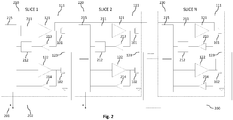
- FIG. 2 which shows a block diagram of a power converter 200 comprising a plurality of inverter stages 210, 220, 230. It can be seen that the inverter stages 210, 220, 230 each comprise a level shifting unit 211 between a respective logic unit 215 and the respective high side driver 211.
- a power converter 200 may comprise a plurality of inverter stages 210, 220, 230 (also referred to as slices) which are arranged in parallel, in order to enable the power converter 200 to drive relatively large loads.
- inverter stages 210, 220, 230 also referred to as slices
- the use of different numbers of inverter stages 210, 220, 230 makes the power converter 200 modular and easily configurable for different load current requirements.
- the power converter 200 of Fig. 2 comprises N parallel inverter stages 210, 220, 230, with N greater than 1.
- the inverter stages 210, 220, 230 are designed in an equal manner.
- each inverter stage 210, 220, 230 comprises a half bridge or inverter with a high side switch 101 and a low side switch 102, and with respective drivers 121, 122.
- the high side switch 101 and the low side switch 102 of an inverter are arranged in series between the input voltage 111 and ground.
- the midpoints 123 between the inverters of the different inverter stages 210, 220, 230 may be coupled with one another and with an inductor 103 (as illustrated in Fig. 1b ).
- Each inverter stage 210, 220, 230 further comprises a level shifting unit 211 which is configured to shift the level of the control signal from a logic voltage level to a drive voltage level.
- the control signal (at the logic voltage level) may be generated by the logic unit 215 of an inverter stage 210, 220, 230.
- the control signal may be generated based on one or more controller signals 201, 202 from a controller (not shown) of the power converter 200.
- the one or more controller signals 201, 202 may comprise a pulse width modulated (pwm) and/or a pulse frequency modulated (pfm) signal.
- the one or more controller signals 201, 202 may comprise a controller signal 201 for enabling (i.e. closing) the high side switch 101 and/or a controller signal 202 for enabling (i.e. closing) the low side switch 102.
- the logic unit 215 of an inverter stage 210, 220, 230 may be configured to generate the control signals for the high side switch 101 and for the low side switch 201.
- the control signal for the high side switch 101 may be referred to as the high side control signal and the control signal for the low side switch 102 may be referred to as the low side control signal.
- the control signals may be generated such that a shoot-through of the respective inverter stage 210, 220, 230 is prevented.
- a shoot-through of an inverter stage 210, 220, 230 may occur if the high side switch 101 and the low side switch 102 of the inverter stage 210, 220, 230 are closed concurrently, thereby generating a short-circuit between the input voltage 111 and ground.
- Such a shoot-through may be avoided by ensuring that the high side switch 101 of the inverter stage 210, 220, 230 is triggered to be closed only once the low side switch 102 of the inverter stage 210, 220, 230 is open, and vice versa.
- the inverter stages 210, 220, 230 may comprise feedback units 213, 214 which are configured to provide a feedback to the logic unit 215 regarding the drive signals (i.e. the gate voltages) of the switches 101, 102, respectively.
- an inverter stage 210, 220, 230 may comprise a high side feedback unit 213 for providing a feedback (i.e. a high side feedback signal) regarding the drive signal of the high side switch 101 to the logic unit 215.
- the high side feedback signal may be level shifted from the drive voltage level to the logic voltage level using an inverse level shifting unit 212.
- an inverter stage 210, 220, 230 may comprise a low side feedback unit 214 for providing a feedback (i.e. a low side feedback signal) regarding the drive signal of the low side switch 101 to the logic unit 215.
- the drive signal of the low side switch 101 is typically related to ground, no level shifting is required for the low side switch 101.
- each slice 210, 220, 230 contributes to the total power dissipation of the power converter 200 in a static and dynamic manner.
- a significant portion of the static power dissipation of a slice 210, 220, 230 is typically due to the level shifting which is performed in each slice 210, 220, 230, in order to drive the high side switches 101 at the drive voltage level.
- a power converter comprising a plurality of parallel inverter stages, wherein at least some of the inverter stages have a different structure.
- a power converter which comprises at least one master inverter stage, as well as one or more slave inverter stages, which are arranged in parallel.
- Fig. 3 shows a block diagram of an example power converter 300 comprising a master inverter stage (or a master slice) 310, as well as a plurality of slave inverter stages (or slave slices) 320, 330.
- the master inverter stage 310 comprises a logic unit 215 for generating the control signals at logic voltage level for the high side switches 101 and the low side switches 102 of the master inverter stage 310 and of the one or more slave inverter stages 320, 330. Furthermore, the master inverter stage 310 comprises a level shifting unit 211 for converting the high side control signal from the logic voltage level to the drive voltage level. The high side control signal at drive voltage level may be provided to the high side driver 121 of the master inverter stage 310 and to the high side drivers 121 of the one or more slave inverter stages 320, 330.
- the power converter 300 comprises only a single level shifting unit 211 (within the master inverter stage 310) for a plurality of inverter stages 310, 320, 330, thereby reducing the power dissipation of the power converter 300.
- the master inverter stage 310 may comprise an inverse level shifting unit 212 for converting the high side feedback signal from the drive voltage level to the logic voltage level. Furthermore, the master inverter stage 310 may comprise a combining unit 311 for combining the high side feedback signals from the master inverter stage 310 and from the one or more slave inverter stages 320, 330. The combining unit 311 may be configured to generate a single combined high side feedback signal from the high side feedback signals of the master inverter stage 310 and of the one or more slave inverter stages 320, 330.
- the combining unit 311 may comprise an AND gate configured to generate the combined high side feedback signal to be at low level only subject to all contributing high side feedback signals being at low level, and to be at high level only subject to all contributing high side feedback signals being at high level.
- the inverse level shifting unit 212 may be configured to shift the level of the combined high side feedback signal from the drive voltage level to the logic voltage level.
- the master inverter stage 310 may comprise a low side combining unit 312 (e.g. an AND gate) configured to generate a combined low side feedback signal from the low side feedback signal of the master inverter stage 310 and of the one or more slave inverter stages 320, 330.
- a low side combining unit 312 e.g. an AND gate
- the logic unit 215 of the master inverter stage 310 may be configured to receive the combined high side feedback signal and the combined low side feedback signal. Furthermore, the logic unit 215 may be configured to prevent a shoot-through of the inverter stages 310, 320, 330 based on the combined high side feedback signal and based on the combined low side feedback signal. In particular, the logic unit 215 may be configured to ensure that none of the high side switches 101 of the power converter 300 is switched on, while any one of the low side switches 102 of the power converter 300 is still on, and/or that none of the low side switches 102 of the power converter 300 is switched on, while any one of the high side switches 101 of the power converter 300 is still on.
- the logic unit 215 is configured to prevent shoot-through situations that may occur across different inverter stages 310, 320, 330 (e.g. because the high side switch 101 of a first inverter stage 320 and the low side switch 102 of a second inverter stage 330 are in on-state concurrently). Due to its capacity for preventing shoot-through situations, the logic unit 215 may also be referred to as an anti shoot-through unit.
- the slave inverter stages 320, 330 do not comprise level shifting units 211 and inverse level shifting units 212.
- Such units 211, 212 are only comprised within the master inverter stage 310. As a result of this, the power dissipation of the power converter 300 is substantially reduced.
- the slave inverter stages 320, 330 do not comprise logic units 215 for generating the drive signals and for preventing shoot-through.
- the power converter 300 of Fig. 3 comprises only a single logic unit 215 within the master inverter stage 310, as well as combining units 311, 312 for combining the feedback signals from the different inverter stages 310, 320, 330.
- shoot-through protection can be improved, because in contrast to the structure of Fig. 2 , the structure of Fig. 3 allows the detection of a shoot-through across different inverter stages 320, 330, which typically cannot be detected using the structure of Fig. 2 .
- the use of only a single logic unit 215 is beneficial with respect to power and space consumption.
- a power converter 300 which comprises only a single slice 310 (referred to as the master slice) having the complete functionality of an inverter stage (notably with respect to level shifting and shoot-through prevention).
- the other slices (referred to as the slave slices) only comprise the power switches 101, 102 and the respective drivers 121, 122.
- This slice configuration allows for an improved efficiency and for a centralized inverter stage control.
- the efficiency improvement is due to the fact that the slave slices do not comprise level shift devices, thereby reducing energy consumption during normal operation of the power converter 300.
- the logic unit 215 may be used for shoot-through protection.
- the power converter 300 of Fig. 3 makes use of only a single logic unit 215 for providing shoot-through protection for a plurality of inverter stages 310, 320, 330. As a result of this, the required silicon area for the logic of the power converter 300 may be reduced.
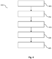
- Fig. 4 shows a flow chart of a method 400 according to claim 14 for driving the high side switches 101 of a power converter 300 comprising a first and a second inverter stage 310, 320.
- the method 400 comprises providing 401 a first half bridge for the first inverter stage 310.
- the first half bridge comprises a first high side switch 101 and a first low side switch 102 which are arranged in series between the input voltage 111 and a reference voltage (e.g. ground).
- the method 400 comprises providing 402 a first high side driver for generating a first drive signal for the first high side switch, subject to a high side control signal at a drive voltage level.
- the method 400 comprises providing 403 a second half bridge for the second inverter stage 320, wherein the second half bridge comprises a second high side switch 101 and a second low side switch 102 which are arranged in series between the input voltage 111 and the reference voltage.
- the method 400 further comprises providing 404 a second high side driver 121 for generating a second drive signal for the second high side switch 101, subject to the high side control signal at the drive voltage level.
- the method 400 comprises providing 405 a level shifting unit 211 configured to convert a high side control signal at a logic voltage level into the high side control signal at the drive voltage level for driving the first and second high side switches 101.
- the method further comprises providing first and second high side feedback units (213) configured to provide first and second high side feedback signals by sensing first and second drive signals for the first and second high side switches (101) and providing a high side combining unit (311) configured to provide a combined high side feedback signal by combining the first and second high side feedback signals; wherein the high side combining unit (311) comprises an AND gate for combining the first and second high side feedback signals; and providing a inverse level shifting unit (212) configured to shift the combined high side feedback signal from the drive voltage level to the logic voltage level.
- a modulator and configurable DC/DC power converter has been described.
- the power converter makes use of a master inverter stage comprising centralized control logic and centralized level shifting.
- the size of the power converter may be reduced and/or the power consumption of the power converter may be reduced.
- the description and drawings merely illustrate the principles of the proposed methods and systems. Those skilled in the art will be able to implement various arrangements that, although not explicitly described or shown herein, embody the principles of the invention as defined by the appended claims.
Landscapes
- Engineering & Computer Science (AREA)
- Power Engineering (AREA)
- Dc-Dc Converters (AREA)
- Inverter Devices (AREA)
Claims (14)
- Leistungswandler (300), der dafür konfiguriert ist, eine elektrische Energie bei einer Eingangsspannung (111) in eine elektrische Leistung bei einer Ausgangsspannung (112) umzuwandeln, wobei der Leistungswandler (300) mindestens umfasst:- eine erste Wechselrichterstufe (310) mit- einer ersten Halbbrücke umfassend einen ersten High-Side-Schalter (101) und einen ersten Low-Side-Schalter (102), die zwischen der Eingangsspannung (111) und einer Bezugsspannung in Reihe geschaltet sind;- einem ersten High-Side-Treiber (121) zum Bereitstellen eines ersten Ansteuerungssignals für den ersten High-Side-Schalter (101) abhängig von einem High-Side-Steuersignal auf einem Ansteuerungsspannungspegel; und- einer ersten High-Side-Rückkopplungseinheit (213), die dafür konfiguriert ist, ein erstes High-Side-Rückkopplungssignal durch Erfassen des ersten Ansteuerungssignals für den ersten High-Side-Schalter (101) bereitzustellen;- eine zweite Wechselrichterstufe (320) mitdadurch gekennzeichnet, dass er weiterhin umfasst:- einer zweiten Halbbrücke umfassend einen zweiten High-Side-Schalter (101) und einen zweiten Low-Side-Schalter (102), die zwischen der Eingangsspannung (111) und der Bezugsspannung in Reihe geschaltet sind;- einem zweiten High-Side-Treiber (121) zum Bereitstellen eines zweiten Ansteuerungssignals für den zweiten High-Side-Schalter (101) abhängig von dem High-Side-Steuersignal auf dem Ansteuerungsspannungspegel; und- einer zweiten High-Side-Rückkopplungseinheit (213), die dafür konfiguriert ist, ein zweites High-Side-Rückkopplungssignal durch Erfassen des zweiten Ansteuerungssignals für den zweiten High-Side-Schalter (101) bereitzustellen; und- eine einzige Pegelverschiebungseinheit (211), die dafür konfiguriert ist, ein High-Side-Steuersignal auf einem Logikspannungspegel in das High-Side-Steuersignal auf dem Ansteuerungsspannungspegel umzuwandeln, um den ersten und den zweiten High-Side-Schalter (101) anzusteuern;- eine High-Side-Kombiniereinheit (311), die dafür konfiguriert ist, ein kombiniertes High-Side-Rückkopplungssignal bereitzustellen, indem sie das erste und das zweite High-Side-Rückkopplungssignal kombiniert; wobei die High-Side-Kombiniereinheit (311) ein UND-Gatter zum Kombinieren des ersten und des zweiten High-Side-Rückkopplungssignals umfasst; und- eine inverse Pegelverschiebungseinheit (212), die dafür konfiguriert ist, das kombinierte High-Side-Rückkopplungssignal von dem Ansteuerungsspannungspegel zum Logikspannungspegel zu verschieben.
- Leistungswandler (300) nach Anspruch 1, wobei ein Versatz zwischen dem Ansteuerungsspannungspegel und dem Logikspannungspegel von einem Pegel der Eingangsspannung (111) abhängt.
- Leistungswandler (300) nach einem der vorhergehenden Ansprüche, wobei- der Leistungswandler (300) nur eine einzige Pegelverschiebungseinheit (211) umfasst, um das High-Side-Steuersignal auf dem Ansteuerungsspannungspegel für die High-Side-Schalter (101) aller Wechselrichterstufen (310, 320, 330) des Leistungswandlers (300) bereitzustellen.
- Leistungswandler (300) nach einem der vorhergehenden Ansprüche, wobei- die erste Wechselrichterstufe (310) weiterhin eine erste Low-Side-Rückkopplungseinheit (214) umfasst, die dafür konfiguriert ist, ein erstes Low-Side-Rückkopplungssignal durch Erfassen eines ersten Ansteuerungssignals für den ersten Low-Side-Schalter (102) bereitzustellen;- die zweite Wechselrichterstufe (320) weiterhin eine zweite Low-Side-Rückkopplungseinheit (214) umfasst, die dafür konfiguriert ist, ein zweites Low-Side-Rückkopplungssignal durch Erfassen eines zweiten Ansteuerungssignals für den zweiten Low-Side-Schalter (102) bereitzustellen;- der Leistungswandler (300) weiterhin eine Low-Side-Kombiniereinheit (312) umfasst, die dafür konfiguriert ist, ein kombiniertes Low-Side-Rückkopplungssignal durch Kombinieren des ersten und des zweiten Low-Side-Rückkopplungssignals bereitzustellen.
- Leistungswandler (300) nach Anspruch 4, wobei die Low-Side-Kombiniereinheit (312) ein UND-Gatter zum Kombinieren des ersten und des zweiten Low-Side-Rückkopplungssignals umfasst.
- Leistungswandler (300) nach einem der vorhergehenden Ansprüche, wobei- der Leistungswandler (300) weiterhin eine Logikeinheit (215) umfasst, die dafür konfiguriert ist, das High-Side-Steuersignal auf dem Logikspannungspegel bereitzustellen, abhängig von einem oder mehreren Reglersignalen (201, 202) von einer Reglereinheit des Leistungswandlers (300); und- die Logikeinheit (215) dafür konfiguriert ist, ein Low-Side-Steuersignal zum Ansteuern des ersten und des zweiten Low-Side-Schalters (102) bereitzustellen.
- Leistungswandler (300) nach Anspruch 6 Bezug nehmend auf Anspruch 4, wobei die Logikeinheit (215) konfiguriert ist zum- Empfangen des kombinierten High-Side-Rückkopplungssignals auf dem Logikspannungspegel;- Empfangen des kombinierten Low-Side-Rückkopplungssignals; und- Bereitstellen des High-Side-Steuersignals und des Low-Side-Steuersignals, sodass sich weder der erste noch der zweite High-Side-Schalter (101) zeitgleich mit entweder dem ersten oder dem zweiten Low-Side-Schalter (102) im Ein-Zustand befindet.
- Leistungswandler (300) nach den Ansprüchen 6 bis 7, wobei- der Leistungswandler (300) nur eine einzelne Logikeinheit (215) zum Bereitstellen des High-Side-Steuersignals für die High-Side-Schalter (101) aller Wechselrichterstufen (310, 320, 330) des Leistungswandlers (300) umfasst.
- Leistungswandler (300) nach den vorhergehenden Ansprüchen, wobei- ein Mittelpunkt (123) zwischen dem ersten High-Side-Schalter (101) und dem ersten Low-Side-Schalter (102) mit einem Mittelpunkt (123) zwischen dem zweiten High-Side-Schalter (101) und dem zweiten Low-Side-Schalter (102) gekoppelt ist; und- die elektrische Leistung bei der Ausgangsspannung (112) von dem Mittelpunkt gezogen wird.
- Leistungswandler (300) nach Anspruch 9, weiterhin umfassend eine Filtereinheit (103, 104), die mit dem Mittelpunkt gekoppelt ist, um die elektrische Leistung bei der Ausgangsspannung (112) bereitzustellen.
- Leistungswandler (300) nach einem der vorhergehenden Ansprüche, wobei- der Leistungswandler (300) eine vorgegebene Anzahl von Wechselrichterstufen (310, 320, 330) umfasst; und- die vorgegebene Anzahl von einem Maß der elektrischen Leistung bei der Ausgangsspannung (112) abhängt, die durch den Leistungswandler (300) bereitzustellen ist.
- Leistungswandler (300) nach einem der vorhergehenden Ansprüche, wobei- ein High-Side-Schalter (101) einen p-Typ-Metalloxid-Halbleitertransistor umfasst; und/oder- ein Low-Side-Schalter (102) einen n-Typ-Metalloxid-Halbleitertransistor umfasst.
- Leistungswandler (300) nach einem der vorhergehenden Ansprüche, wobei ein Ausgang des ersten High-Side-Treibers (121) mit einem Ausgang des zweiten High-Side-Treibers (121) gekoppelt ist.
- Verfahren (400) zum Ansteuern der High-Side-Schalter (101) eines Leistungswandlers (300) umfassend eine erste und eine zweite Wechselrichterstufe (310, 320), wobei das Verfahren (400) mindestens umfasst:- Bereitstellen (401) einer ersten Halbbrücke für die erste Wechselrichterstufe (310), wobei die erste Halbbrücke einen ersten High-Side-Schalter (101) und einen ersten Low-Side-Schalter (102) umfasst, die zwischen der Eingangsspannung (111) und einer Bezugsspannung in Reihe geschaltet sind;- Bereitstellen (402) eines ersten High-Side-Treibers (121) zum Erzeugen eines ersten Ansteuerungssignals für den ersten High-Side-Schalter (101) abhängig von einem High-Side-Steuersignal auf einem Ansteuerungsspannungspegel;- Bereitstellen einer ersten High-Side-Rückkopplungseinheit (213), die dafür konfiguriert ist, ein erstes High-Side-Rückkopplungssignal durch Erfassen des ersten Ansteuerungssignals für den ersten High-Side-Schalter (101) bereitzustellen;- Bereitstellen (403) einer zweiten Halbbrücke für die zweite Wechselrichterstufe (320), wobei die zweite Halbbrücke einen zweiten High-Side-Schalter (101) und einen zweiten Low-Side-Schalter (102) umfasst, die zwischen der Eingangsspannung (111) und der Bezugsspannung in Reihe geschaltet sind;- Bereitstellen (404) eines zweiten High-Side-Treibers (121) zum Erzeugen eines zweiten Ansteuerungssignals für den zweiten High-Side-Schalter (101) abhängig von einem High-Side-Steuersignal auf dem Ansteuerungsspannungspegel;- Bereitstellen einer zweiten High-Side-Rückkopplungseinheit (213), die dafür konfiguriert ist, ein zweites High-Side-Rückkopplungssignal durch Erfassen des zweiten Ansteuerungssignals für den zweiten High-Side-Schalter (101) bereitzustellen; undund gekennzeichnet durch:- Bereitstellen (405) einer einzigen Pegelverschiebungseinheit (211), die dafür konfiguriert ist, ein High-Side-Steuersignal auf einem Logikspannungspegel in das High-Side-Steuersignal auf dem Ansteuerungsspannungspegel umzuwandeln, um den ersten und den zweiten High-Side-Schalter (101) anzusteuern;- Bereitstellen einer High-Side-Kombiniereinheit (311), die dafür konfiguriert ist, ein kombiniertes High-Side-Rückkopplungssignal bereitzustellen, indem sie das erste und das zweite High-Side-Rückkopplungssignal kombiniert; wobei die High-Side-Kombiniereinheit (311) ein UND-Gatter zum Kombinieren des ersten und des zweiten High-Side-Rückkopplungssignals umfasst; und- Bereitstellen einer inversen Pegelverschiebungseinheit (212), die dafür konfiguriert ist, das kombinierte High-Side-Rückkopplungssignal von dem Ansteuerungsspannungspegel zum Logikspannungspegel zu verschieben.
Priority Applications (2)
| Application Number | Priority Date | Filing Date | Title |
|---|---|---|---|
| EP14150649.3A EP2894776B1 (de) | 2014-01-09 | 2014-01-09 | Gleichspannungswandler für hohe Spannungen mit Master/Slave Tiefsetzstellerausgangsstufen |
| US14/445,288 US9559587B2 (en) | 2014-01-09 | 2014-07-29 | High voltage DC/DC converter with master/slave output stage |
Applications Claiming Priority (1)
| Application Number | Priority Date | Filing Date | Title |
|---|---|---|---|
| EP14150649.3A EP2894776B1 (de) | 2014-01-09 | 2014-01-09 | Gleichspannungswandler für hohe Spannungen mit Master/Slave Tiefsetzstellerausgangsstufen |
Publications (2)
| Publication Number | Publication Date |
|---|---|
| EP2894776A1 EP2894776A1 (de) | 2015-07-15 |
| EP2894776B1 true EP2894776B1 (de) | 2017-11-29 |
Family
ID=49886857
Family Applications (1)
| Application Number | Title | Priority Date | Filing Date |
|---|---|---|---|
| EP14150649.3A Active EP2894776B1 (de) | 2014-01-09 | 2014-01-09 | Gleichspannungswandler für hohe Spannungen mit Master/Slave Tiefsetzstellerausgangsstufen |
Country Status (2)
| Country | Link |
|---|---|
| US (1) | US9559587B2 (de) |
| EP (1) | EP2894776B1 (de) |
Families Citing this family (1)
| Publication number | Priority date | Publication date | Assignee | Title |
|---|---|---|---|---|
| WO2017137057A1 (en) * | 2016-02-08 | 2017-08-17 | Abb Schweiz Ag | Switching device for a high voltage power system and an arrangement comprising such a switching device |
Citations (1)
| Publication number | Priority date | Publication date | Assignee | Title |
|---|---|---|---|---|
| US20100231270A1 (en) * | 2009-02-20 | 2010-09-16 | Rohm Co., Ltd. | Switching output circuit |
Family Cites Families (5)
| Publication number | Priority date | Publication date | Assignee | Title |
|---|---|---|---|---|
| JPH03169273A (ja) * | 1989-11-22 | 1991-07-22 | Mitsubishi Electric Corp | スイッチングデバイス駆動回路 |
| DE19604341C2 (de) * | 1996-02-07 | 1998-07-02 | Fraunhofer Ges Forschung | Einrichtung zur Ansteuerung von Schaltelementen, insbesondere MOS-FETS in Brückenzweigpaaren |
| EP1524572B1 (de) * | 2002-07-10 | 2011-12-28 | Marvell World Trade Ltd. | Spannungsversorgungsanordnung und Verfahren |
| KR100595447B1 (ko) * | 2004-03-26 | 2006-07-03 | 삼성전자주식회사 | Dc-dc 컨버터 및 그 제어방법 |
| US7554384B2 (en) * | 2006-06-30 | 2009-06-30 | Intel Corporation | Methods and arrangements for generating a control signal for a power converter |
-
2014
- 2014-01-09 EP EP14150649.3A patent/EP2894776B1/de active Active
- 2014-07-29 US US14/445,288 patent/US9559587B2/en active Active
Patent Citations (1)
| Publication number | Priority date | Publication date | Assignee | Title |
|---|---|---|---|---|
| US20100231270A1 (en) * | 2009-02-20 | 2010-09-16 | Rohm Co., Ltd. | Switching output circuit |
Also Published As
| Publication number | Publication date |
|---|---|
| US20150194889A1 (en) | 2015-07-09 |
| EP2894776A1 (de) | 2015-07-15 |
| US9559587B2 (en) | 2017-01-31 |
Similar Documents
| Publication | Publication Date | Title |
|---|---|---|
| JP5429032B2 (ja) | 電力変換回路 | |
| EP2487786A2 (de) | Leistungswandlervorrichtung mit fünf Stufen | |
| WO2013150573A1 (ja) | 整流回路 | |
| EP2302784A1 (de) | Gleichstrom-Wechselstromumformer | |
| JP5310425B2 (ja) | 電力変換器 | |
| KR20100130161A (ko) | 다상 부스트 컨버터와 그 작동방법 | |
| WO2010117410A1 (en) | Buck converter with iii-nitride switch for substantially increased input-to-output voltage ratio | |
| JP2013070530A (ja) | ゲート駆動回路、電力変換回路、3相インバータ、及びゲート駆動方法 | |
| JP2014135799A (ja) | 電力変換装置 | |
| JP2010088283A (ja) | スナバ回路 | |
| CA3110897A1 (en) | Dual dc-dc converter | |
| US8994437B2 (en) | Semiconductor device and circuit for controlling potential of gate of insulated gate type switching device | |
| US20150092467A1 (en) | Driver Circuit for a Pair of Semiconductor Switches in a Leg of a Three-Level Inverter Half-Bridge | |
| JP5009680B2 (ja) | 開閉装置 | |
| JP5362657B2 (ja) | 電力変換装置 | |
| EP2894776B1 (de) | Gleichspannungswandler für hohe Spannungen mit Master/Slave Tiefsetzstellerausgangsstufen | |
| US9431904B2 (en) | DC/DC converter efficiency improvement for low current levels | |
| US9270180B2 (en) | DC-DC converter with adaptive minimum on-time | |
| US11121549B2 (en) | Power flow control device for controlling the distribution of currents in a mesh network | |
| US12074521B2 (en) | Circuit arrangement for balancing a split DC link | |
| US9436192B2 (en) | Apparatus for PWM gate drive circuit | |
| JP2014023190A (ja) | スイッチング回路 | |
| JP2012175816A (ja) | 減電圧保護回路及びこれを用いたスイッチ駆動装置 | |
| JP2011151788A (ja) | 半導体装置 | |
| CN110663164B (zh) | 具有多个功率模式的功率转换器预驱动器系统 |
Legal Events
| Date | Code | Title | Description |
|---|---|---|---|
| PUAI | Public reference made under article 153(3) epc to a published international application that has entered the european phase |
Free format text: ORIGINAL CODE: 0009012 |
|
| 17P | Request for examination filed |
Effective date: 20140109 |
|
| AK | Designated contracting states |
Kind code of ref document: A1 Designated state(s): AL AT BE BG CH CY CZ DE DK EE ES FI FR GB GR HR HU IE IS IT LI LT LU LV MC MK MT NL NO PL PT RO RS SE SI SK SM TR |
|
| AX | Request for extension of the european patent |
Extension state: BA ME |
|
| R17P | Request for examination filed (corrected) |
Effective date: 20151118 |
|
| RBV | Designated contracting states (corrected) |
Designated state(s): AL AT BE BG CH CY CZ DE DK EE ES FI FR GB GR HR HU IE IS IT LI LT LU LV MC MK MT NL NO PL PT RO RS SE SI SK SM TR |
|
| GRAP | Despatch of communication of intention to grant a patent |
Free format text: ORIGINAL CODE: EPIDOSNIGR1 |
|
| STAA | Information on the status of an ep patent application or granted ep patent |
Free format text: STATUS: GRANT OF PATENT IS INTENDED |
|
| INTG | Intention to grant announced |
Effective date: 20170504 |
|
| GRAS | Grant fee paid |
Free format text: ORIGINAL CODE: EPIDOSNIGR3 |
|
| GRAJ | Information related to disapproval of communication of intention to grant by the applicant or resumption of examination proceedings by the epo deleted |
Free format text: ORIGINAL CODE: EPIDOSDIGR1 |
|
| GRAL | Information related to payment of fee for publishing/printing deleted |
Free format text: ORIGINAL CODE: EPIDOSDIGR3 |
|
| STAA | Information on the status of an ep patent application or granted ep patent |
Free format text: STATUS: REQUEST FOR EXAMINATION WAS MADE |
|
| GRAR | Information related to intention to grant a patent recorded |
Free format text: ORIGINAL CODE: EPIDOSNIGR71 |
|
| STAA | Information on the status of an ep patent application or granted ep patent |
Free format text: STATUS: GRANT OF PATENT IS INTENDED |
|
| GRAA | (expected) grant |
Free format text: ORIGINAL CODE: 0009210 |
|
| STAA | Information on the status of an ep patent application or granted ep patent |
Free format text: STATUS: THE PATENT HAS BEEN GRANTED |
|
| INTC | Intention to grant announced (deleted) | ||
| AK | Designated contracting states |
Kind code of ref document: B1 Designated state(s): AL AT BE BG CH CY CZ DE DK EE ES FI FR GB GR HR HU IE IS IT LI LT LU LV MC MK MT NL NO PL PT RO RS SE SI SK SM TR |
|
| INTG | Intention to grant announced |
Effective date: 20171024 |
|
| REG | Reference to a national code |
Ref country code: CH Ref legal event code: EP |
|
| REG | Reference to a national code |
Ref country code: AT Ref legal event code: REF Ref document number: 951258 Country of ref document: AT Kind code of ref document: T Effective date: 20171215 |
|
| REG | Reference to a national code |
Ref country code: IE Ref legal event code: FG4D |
|
| REG | Reference to a national code |
Ref country code: DE Ref legal event code: R096 Ref document number: 602014017769 Country of ref document: DE |
|
| REG | Reference to a national code |
Ref country code: NL Ref legal event code: MP Effective date: 20171129 |
|
| REG | Reference to a national code |
Ref country code: LT Ref legal event code: MG4D |
|
| REG | Reference to a national code |
Ref country code: AT Ref legal event code: MK05 Ref document number: 951258 Country of ref document: AT Kind code of ref document: T Effective date: 20171129 |
|
| PG25 | Lapsed in a contracting state [announced via postgrant information from national office to epo] |
Ref country code: ES Free format text: LAPSE BECAUSE OF FAILURE TO SUBMIT A TRANSLATION OF THE DESCRIPTION OR TO PAY THE FEE WITHIN THE PRESCRIBED TIME-LIMIT Effective date: 20171129 Ref country code: FI Free format text: LAPSE BECAUSE OF FAILURE TO SUBMIT A TRANSLATION OF THE DESCRIPTION OR TO PAY THE FEE WITHIN THE PRESCRIBED TIME-LIMIT Effective date: 20171129 Ref country code: LT Free format text: LAPSE BECAUSE OF FAILURE TO SUBMIT A TRANSLATION OF THE DESCRIPTION OR TO PAY THE FEE WITHIN THE PRESCRIBED TIME-LIMIT Effective date: 20171129 Ref country code: SE Free format text: LAPSE BECAUSE OF FAILURE TO SUBMIT A TRANSLATION OF THE DESCRIPTION OR TO PAY THE FEE WITHIN THE PRESCRIBED TIME-LIMIT Effective date: 20171129 Ref country code: NO Free format text: LAPSE BECAUSE OF FAILURE TO SUBMIT A TRANSLATION OF THE DESCRIPTION OR TO PAY THE FEE WITHIN THE PRESCRIBED TIME-LIMIT Effective date: 20180228 |
|
| PG25 | Lapsed in a contracting state [announced via postgrant information from national office to epo] |
Ref country code: LV Free format text: LAPSE BECAUSE OF FAILURE TO SUBMIT A TRANSLATION OF THE DESCRIPTION OR TO PAY THE FEE WITHIN THE PRESCRIBED TIME-LIMIT Effective date: 20171129 Ref country code: HR Free format text: LAPSE BECAUSE OF FAILURE TO SUBMIT A TRANSLATION OF THE DESCRIPTION OR TO PAY THE FEE WITHIN THE PRESCRIBED TIME-LIMIT Effective date: 20171129 Ref country code: AT Free format text: LAPSE BECAUSE OF FAILURE TO SUBMIT A TRANSLATION OF THE DESCRIPTION OR TO PAY THE FEE WITHIN THE PRESCRIBED TIME-LIMIT Effective date: 20171129 Ref country code: RS Free format text: LAPSE BECAUSE OF FAILURE TO SUBMIT A TRANSLATION OF THE DESCRIPTION OR TO PAY THE FEE WITHIN THE PRESCRIBED TIME-LIMIT Effective date: 20171129 Ref country code: BG Free format text: LAPSE BECAUSE OF FAILURE TO SUBMIT A TRANSLATION OF THE DESCRIPTION OR TO PAY THE FEE WITHIN THE PRESCRIBED TIME-LIMIT Effective date: 20180228 Ref country code: GR Free format text: LAPSE BECAUSE OF FAILURE TO SUBMIT A TRANSLATION OF THE DESCRIPTION OR TO PAY THE FEE WITHIN THE PRESCRIBED TIME-LIMIT Effective date: 20180301 |
|
| PG25 | Lapsed in a contracting state [announced via postgrant information from national office to epo] |
Ref country code: NL Free format text: LAPSE BECAUSE OF FAILURE TO SUBMIT A TRANSLATION OF THE DESCRIPTION OR TO PAY THE FEE WITHIN THE PRESCRIBED TIME-LIMIT Effective date: 20171129 |
|
| PG25 | Lapsed in a contracting state [announced via postgrant information from national office to epo] |
Ref country code: CZ Free format text: LAPSE BECAUSE OF FAILURE TO SUBMIT A TRANSLATION OF THE DESCRIPTION OR TO PAY THE FEE WITHIN THE PRESCRIBED TIME-LIMIT Effective date: 20171129 Ref country code: SK Free format text: LAPSE BECAUSE OF FAILURE TO SUBMIT A TRANSLATION OF THE DESCRIPTION OR TO PAY THE FEE WITHIN THE PRESCRIBED TIME-LIMIT Effective date: 20171129 Ref country code: CY Free format text: LAPSE BECAUSE OF FAILURE TO SUBMIT A TRANSLATION OF THE DESCRIPTION OR TO PAY THE FEE WITHIN THE PRESCRIBED TIME-LIMIT Effective date: 20171129 Ref country code: EE Free format text: LAPSE BECAUSE OF FAILURE TO SUBMIT A TRANSLATION OF THE DESCRIPTION OR TO PAY THE FEE WITHIN THE PRESCRIBED TIME-LIMIT Effective date: 20171129 Ref country code: DK Free format text: LAPSE BECAUSE OF FAILURE TO SUBMIT A TRANSLATION OF THE DESCRIPTION OR TO PAY THE FEE WITHIN THE PRESCRIBED TIME-LIMIT Effective date: 20171129 |
|
| REG | Reference to a national code |
Ref country code: DE Ref legal event code: R097 Ref document number: 602014017769 Country of ref document: DE |
|
| PG25 | Lapsed in a contracting state [announced via postgrant information from national office to epo] |
Ref country code: PL Free format text: LAPSE BECAUSE OF FAILURE TO SUBMIT A TRANSLATION OF THE DESCRIPTION OR TO PAY THE FEE WITHIN THE PRESCRIBED TIME-LIMIT Effective date: 20171129 Ref country code: SM Free format text: LAPSE BECAUSE OF FAILURE TO SUBMIT A TRANSLATION OF THE DESCRIPTION OR TO PAY THE FEE WITHIN THE PRESCRIBED TIME-LIMIT Effective date: 20171129 Ref country code: RO Free format text: LAPSE BECAUSE OF FAILURE TO SUBMIT A TRANSLATION OF THE DESCRIPTION OR TO PAY THE FEE WITHIN THE PRESCRIBED TIME-LIMIT Effective date: 20171129 Ref country code: IT Free format text: LAPSE BECAUSE OF FAILURE TO SUBMIT A TRANSLATION OF THE DESCRIPTION OR TO PAY THE FEE WITHIN THE PRESCRIBED TIME-LIMIT Effective date: 20171129 |
|
| REG | Reference to a national code |
Ref country code: CH Ref legal event code: PL |
|
| PLBE | No opposition filed within time limit |
Free format text: ORIGINAL CODE: 0009261 |
|
| STAA | Information on the status of an ep patent application or granted ep patent |
Free format text: STATUS: NO OPPOSITION FILED WITHIN TIME LIMIT |
|
| PG25 | Lapsed in a contracting state [announced via postgrant information from national office to epo] |
Ref country code: LU Free format text: LAPSE BECAUSE OF NON-PAYMENT OF DUE FEES Effective date: 20180109 Ref country code: FR Free format text: LAPSE BECAUSE OF NON-PAYMENT OF DUE FEES Effective date: 20180131 |
|
| REG | Reference to a national code |
Ref country code: IE Ref legal event code: MM4A |
|
| REG | Reference to a national code |
Ref country code: FR Ref legal event code: ST Effective date: 20180928 |
|
| 26N | No opposition filed |
Effective date: 20180830 |
|
| REG | Reference to a national code |
Ref country code: BE Ref legal event code: MM Effective date: 20180131 |
|
| PG25 | Lapsed in a contracting state [announced via postgrant information from national office to epo] |
Ref country code: LI Free format text: LAPSE BECAUSE OF NON-PAYMENT OF DUE FEES Effective date: 20180131 Ref country code: BE Free format text: LAPSE BECAUSE OF NON-PAYMENT OF DUE FEES Effective date: 20180131 Ref country code: SI Free format text: LAPSE BECAUSE OF FAILURE TO SUBMIT A TRANSLATION OF THE DESCRIPTION OR TO PAY THE FEE WITHIN THE PRESCRIBED TIME-LIMIT Effective date: 20171129 Ref country code: CH Free format text: LAPSE BECAUSE OF NON-PAYMENT OF DUE FEES Effective date: 20180131 |
|
| PG25 | Lapsed in a contracting state [announced via postgrant information from national office to epo] |
Ref country code: IE Free format text: LAPSE BECAUSE OF NON-PAYMENT OF DUE FEES Effective date: 20180109 |
|
| PG25 | Lapsed in a contracting state [announced via postgrant information from national office to epo] |
Ref country code: MC Free format text: LAPSE BECAUSE OF FAILURE TO SUBMIT A TRANSLATION OF THE DESCRIPTION OR TO PAY THE FEE WITHIN THE PRESCRIBED TIME-LIMIT Effective date: 20171129 |
|
| PG25 | Lapsed in a contracting state [announced via postgrant information from national office to epo] |
Ref country code: MT Free format text: LAPSE BECAUSE OF NON-PAYMENT OF DUE FEES Effective date: 20180109 |
|
| PG25 | Lapsed in a contracting state [announced via postgrant information from national office to epo] |
Ref country code: TR Free format text: LAPSE BECAUSE OF FAILURE TO SUBMIT A TRANSLATION OF THE DESCRIPTION OR TO PAY THE FEE WITHIN THE PRESCRIBED TIME-LIMIT Effective date: 20171129 |
|
| PG25 | Lapsed in a contracting state [announced via postgrant information from national office to epo] |
Ref country code: PT Free format text: LAPSE BECAUSE OF FAILURE TO SUBMIT A TRANSLATION OF THE DESCRIPTION OR TO PAY THE FEE WITHIN THE PRESCRIBED TIME-LIMIT Effective date: 20171129 |
|
| PG25 | Lapsed in a contracting state [announced via postgrant information from national office to epo] |
Ref country code: HU Free format text: LAPSE BECAUSE OF FAILURE TO SUBMIT A TRANSLATION OF THE DESCRIPTION OR TO PAY THE FEE WITHIN THE PRESCRIBED TIME-LIMIT; INVALID AB INITIO Effective date: 20140109 Ref country code: MK Free format text: LAPSE BECAUSE OF NON-PAYMENT OF DUE FEES Effective date: 20171129 |
|
| PG25 | Lapsed in a contracting state [announced via postgrant information from national office to epo] |
Ref country code: AL Free format text: LAPSE BECAUSE OF FAILURE TO SUBMIT A TRANSLATION OF THE DESCRIPTION OR TO PAY THE FEE WITHIN THE PRESCRIBED TIME-LIMIT Effective date: 20171129 Ref country code: IS Free format text: LAPSE BECAUSE OF FAILURE TO SUBMIT A TRANSLATION OF THE DESCRIPTION OR TO PAY THE FEE WITHIN THE PRESCRIBED TIME-LIMIT Effective date: 20180329 |
|
| PGFP | Annual fee paid to national office [announced via postgrant information from national office to epo] |
Ref country code: GB Payment date: 20231214 Year of fee payment: 11 |
|
| PGFP | Annual fee paid to national office [announced via postgrant information from national office to epo] |
Ref country code: DE Payment date: 20231218 Year of fee payment: 11 |