EP2889682A1 - Anzeigevorrichtung mit redundanter Transistorstruktur - Google Patents
Anzeigevorrichtung mit redundanter Transistorstruktur Download PDFInfo
- Publication number
- EP2889682A1 EP2889682A1 EP14174907.7A EP14174907A EP2889682A1 EP 2889682 A1 EP2889682 A1 EP 2889682A1 EP 14174907 A EP14174907 A EP 14174907A EP 2889682 A1 EP2889682 A1 EP 2889682A1
- Authority
- EP
- European Patent Office
- Prior art keywords
- electrode unit
- electrode
- transistor
- display device
- shape
- Prior art date
- Legal status (The legal status is an assumption and is not a legal conclusion. Google has not performed a legal analysis and makes no representation as to the accuracy of the status listed.)
- Granted
Links
Images


Classifications
-
- G—PHYSICS
- G09—EDUCATION; CRYPTOGRAPHY; DISPLAY; ADVERTISING; SEALS
- G09G—ARRANGEMENTS OR CIRCUITS FOR CONTROL OF INDICATING DEVICES USING STATIC MEANS TO PRESENT VARIABLE INFORMATION
- G09G3/00—Control arrangements or circuits, of interest only in connection with visual indicators other than cathode-ray tubes
- G09G3/20—Control arrangements or circuits, of interest only in connection with visual indicators other than cathode-ray tubes for presentation of an assembly of a number of characters, e.g. a page, by composing the assembly by combination of individual elements arranged in a matrix no fixed position being assigned to or needed to be assigned to the individual characters or partial characters
-
- G—PHYSICS
- G02—OPTICS
- G02F—OPTICAL DEVICES OR ARRANGEMENTS FOR THE CONTROL OF LIGHT BY MODIFICATION OF THE OPTICAL PROPERTIES OF THE MEDIA OF THE ELEMENTS INVOLVED THEREIN; NON-LINEAR OPTICS; FREQUENCY-CHANGING OF LIGHT; OPTICAL LOGIC ELEMENTS; OPTICAL ANALOGUE/DIGITAL CONVERTERS
- G02F1/00—Devices or arrangements for the control of the intensity, colour, phase, polarisation or direction of light arriving from an independent light source, e.g. switching, gating or modulating; Non-linear optics
- G02F1/01—Devices or arrangements for the control of the intensity, colour, phase, polarisation or direction of light arriving from an independent light source, e.g. switching, gating or modulating; Non-linear optics for the control of the intensity, phase, polarisation or colour
- G02F1/13—Devices or arrangements for the control of the intensity, colour, phase, polarisation or direction of light arriving from an independent light source, e.g. switching, gating or modulating; Non-linear optics for the control of the intensity, phase, polarisation or colour based on liquid crystals, e.g. single liquid crystal display cells
- G02F1/133—Constructional arrangements; Operation of liquid crystal cells; Circuit arrangements
- G02F1/136—Liquid crystal cells structurally associated with a semi-conducting layer or substrate, e.g. cells forming part of an integrated circuit
- G02F1/1362—Active matrix addressed cells
- G02F1/136259—Repairing; Defects
-
- H—ELECTRICITY
- H10—SEMICONDUCTOR DEVICES; ELECTRIC SOLID-STATE DEVICES NOT OTHERWISE PROVIDED FOR
- H10D—INORGANIC ELECTRIC SEMICONDUCTOR DEVICES
- H10D86/00—Integrated devices formed in or on insulating or conducting substrates, e.g. formed in silicon-on-insulator [SOI] substrates or on stainless steel or glass substrates
- H10D86/40—Integrated devices formed in or on insulating or conducting substrates, e.g. formed in silicon-on-insulator [SOI] substrates or on stainless steel or glass substrates characterised by multiple TFTs
- H10D86/60—Integrated devices formed in or on insulating or conducting substrates, e.g. formed in silicon-on-insulator [SOI] substrates or on stainless steel or glass substrates characterised by multiple TFTs wherein the TFTs are in active matrices
-
- G—PHYSICS
- G09—EDUCATION; CRYPTOGRAPHY; DISPLAY; ADVERTISING; SEALS
- G09F—DISPLAYING; ADVERTISING; SIGNS; LABELS OR NAME-PLATES; SEALS
- G09F9/00—Indicating arrangements for variable information in which the information is built-up on a support by selection or combination of individual elements
- G09F9/30—Indicating arrangements for variable information in which the information is built-up on a support by selection or combination of individual elements in which the desired character or characters are formed by combining individual elements
-
- H—ELECTRICITY
- H10—SEMICONDUCTOR DEVICES; ELECTRIC SOLID-STATE DEVICES NOT OTHERWISE PROVIDED FOR
- H10D—INORGANIC ELECTRIC SEMICONDUCTOR DEVICES
- H10D30/00—Field-effect transistors [FET]
- H10D30/60—Insulated-gate field-effect transistors [IGFET]
- H10D30/67—Thin-film transistors [TFT]
- H10D30/6729—Thin-film transistors [TFT] characterised by the electrodes
- H10D30/673—Thin-film transistors [TFT] characterised by the electrodes characterised by the shapes, relative sizes or dispositions of the gate electrodes
-
- H—ELECTRICITY
- H10—SEMICONDUCTOR DEVICES; ELECTRIC SOLID-STATE DEVICES NOT OTHERWISE PROVIDED FOR
- H10D—INORGANIC ELECTRIC SEMICONDUCTOR DEVICES
- H10D30/00—Field-effect transistors [FET]
- H10D30/60—Insulated-gate field-effect transistors [IGFET]
- H10D30/67—Thin-film transistors [TFT]
- H10D30/674—Thin-film transistors [TFT] characterised by the active materials
- H10D30/6741—Group IV materials, e.g. germanium or silicon carbide
- H10D30/6743—Silicon
- H10D30/6745—Polycrystalline or microcrystalline silicon
-
- H—ELECTRICITY
- H10—SEMICONDUCTOR DEVICES; ELECTRIC SOLID-STATE DEVICES NOT OTHERWISE PROVIDED FOR
- H10D—INORGANIC ELECTRIC SEMICONDUCTOR DEVICES
- H10D30/00—Field-effect transistors [FET]
- H10D30/60—Insulated-gate field-effect transistors [IGFET]
- H10D30/67—Thin-film transistors [TFT]
- H10D30/674—Thin-film transistors [TFT] characterised by the active materials
- H10D30/6741—Group IV materials, e.g. germanium or silicon carbide
- H10D30/6743—Silicon
- H10D30/6746—Amorphous silicon
-
- H—ELECTRICITY
- H10—SEMICONDUCTOR DEVICES; ELECTRIC SOLID-STATE DEVICES NOT OTHERWISE PROVIDED FOR
- H10D—INORGANIC ELECTRIC SEMICONDUCTOR DEVICES
- H10D30/00—Field-effect transistors [FET]
- H10D30/60—Insulated-gate field-effect transistors [IGFET]
- H10D30/67—Thin-film transistors [TFT]
- H10D30/674—Thin-film transistors [TFT] characterised by the active materials
- H10D30/6755—Oxide semiconductors, e.g. zinc oxide, copper aluminium oxide or cadmium stannate
-
- H—ELECTRICITY
- H10—SEMICONDUCTOR DEVICES; ELECTRIC SOLID-STATE DEVICES NOT OTHERWISE PROVIDED FOR
- H10D—INORGANIC ELECTRIC SEMICONDUCTOR DEVICES
- H10D86/00—Integrated devices formed in or on insulating or conducting substrates, e.g. formed in silicon-on-insulator [SOI] substrates or on stainless steel or glass substrates
- H10D86/40—Integrated devices formed in or on insulating or conducting substrates, e.g. formed in silicon-on-insulator [SOI] substrates or on stainless steel or glass substrates characterised by multiple TFTs
- H10D86/421—Integrated devices formed in or on insulating or conducting substrates, e.g. formed in silicon-on-insulator [SOI] substrates or on stainless steel or glass substrates characterised by multiple TFTs having a particular composition, shape or crystalline structure of the active layer
- H10D86/423—Integrated devices formed in or on insulating or conducting substrates, e.g. formed in silicon-on-insulator [SOI] substrates or on stainless steel or glass substrates characterised by multiple TFTs having a particular composition, shape or crystalline structure of the active layer comprising semiconductor materials not belonging to the Group IV, e.g. InGaZnO
-
- H—ELECTRICITY
- H10—SEMICONDUCTOR DEVICES; ELECTRIC SOLID-STATE DEVICES NOT OTHERWISE PROVIDED FOR
- H10D—INORGANIC ELECTRIC SEMICONDUCTOR DEVICES
- H10D86/00—Integrated devices formed in or on insulating or conducting substrates, e.g. formed in silicon-on-insulator [SOI] substrates or on stainless steel or glass substrates
- H10D86/40—Integrated devices formed in or on insulating or conducting substrates, e.g. formed in silicon-on-insulator [SOI] substrates or on stainless steel or glass substrates characterised by multiple TFTs
- H10D86/441—Interconnections, e.g. scanning lines
-
- H—ELECTRICITY
- H10—SEMICONDUCTOR DEVICES; ELECTRIC SOLID-STATE DEVICES NOT OTHERWISE PROVIDED FOR
- H10D—INORGANIC ELECTRIC SEMICONDUCTOR DEVICES
- H10D86/00—Integrated devices formed in or on insulating or conducting substrates, e.g. formed in silicon-on-insulator [SOI] substrates or on stainless steel or glass substrates
- H10D86/40—Integrated devices formed in or on insulating or conducting substrates, e.g. formed in silicon-on-insulator [SOI] substrates or on stainless steel or glass substrates characterised by multiple TFTs
- H10D86/481—Integrated devices formed in or on insulating or conducting substrates, e.g. formed in silicon-on-insulator [SOI] substrates or on stainless steel or glass substrates characterised by multiple TFTs integrated with passive devices, e.g. auxiliary capacitors
-
- G—PHYSICS
- G02—OPTICS
- G02F—OPTICAL DEVICES OR ARRANGEMENTS FOR THE CONTROL OF LIGHT BY MODIFICATION OF THE OPTICAL PROPERTIES OF THE MEDIA OF THE ELEMENTS INVOLVED THEREIN; NON-LINEAR OPTICS; FREQUENCY-CHANGING OF LIGHT; OPTICAL LOGIC ELEMENTS; OPTICAL ANALOGUE/DIGITAL CONVERTERS
- G02F1/00—Devices or arrangements for the control of the intensity, colour, phase, polarisation or direction of light arriving from an independent light source, e.g. switching, gating or modulating; Non-linear optics
- G02F1/01—Devices or arrangements for the control of the intensity, colour, phase, polarisation or direction of light arriving from an independent light source, e.g. switching, gating or modulating; Non-linear optics for the control of the intensity, phase, polarisation or colour
- G02F1/13—Devices or arrangements for the control of the intensity, colour, phase, polarisation or direction of light arriving from an independent light source, e.g. switching, gating or modulating; Non-linear optics for the control of the intensity, phase, polarisation or colour based on liquid crystals, e.g. single liquid crystal display cells
- G02F1/133—Constructional arrangements; Operation of liquid crystal cells; Circuit arrangements
- G02F1/136—Liquid crystal cells structurally associated with a semi-conducting layer or substrate, e.g. cells forming part of an integrated circuit
- G02F1/1362—Active matrix addressed cells
- G02F1/136259—Repairing; Defects
- G02F1/136268—Switch defects
Definitions
- a display panel for use in a display device such as a liquid display device or an organic light-emitting display device is, in general, provided with at least one transistor for displaying an image.
- a transistor within each pixel in a display panel is fabricated through a number of processes. During the processes, fine foreign substances, particles, and/or impurities may undesirably be included in the transistors (in particular, in the channel regions). In such an instance, the transistor may be electrically shorted or disconnected and, thus, the transistor may not function normally. This may cause a pixel defect which changes the corresponding pixel into a bright dot or a dark dot.
- Such a pixel defect which changes a pixel into a bright dot or a dark dot may considerably degrade the quality of the image of display devices and reduce the yield of display panel production.
- Yet another aspect of the present invention is to provide a display device having a redundant transistor structure which does not reduce the aperture ratio of the display panel as well as enables a repair process of the display panel.
- the present invention may provide a display device having a redundant transistor structure which enables a repair process in such a manner that, when a foreign substance exists in a transistor and causes a pixel defect, the corresponding pixel can still function as a normal pixel.
- the gate drive unit 130 may include a plurality of gate drive integrated circuits.
- the plurality of gate drive integrated circuits may be connected to a bonding pad of the display panel 110 through a Tape Automated Bonding (TAB) method or a Chip On Glass (COG) method, or implemented in a Gate In Panel (GIP) type and directly formed in the display panel 110.
- TAB Tape Automated Bonding
- COG Chip On Glass
- GIP Gate In Panel
- the plurality of gate drive integrated circuits may be integrated and formed in the display panel 110.
- the first transistor TR1 and the second transistor TR2 are connected in parallel to each other to perform a switching operation.
- the switching operation in a normal pixel is performed in the same manner that one transistor TR performs its switching operation.
- the first transistor TR1 includes the first electrode e1 of the first electrode unit E1, the second electrode e2 of the second electrode unit E2, the third electrode unit E3, and the channel CH1 that interconnects the first electrode e1 of the first electrode unit E1 and the second electrode e2 of the second electrode unit E2.
- the second transistor TR2 includes the first electrode e1' of the first electrode unit E1, the second electrode e2' of the second electrode unit E2, the third electrode unit E3, and the channel CH2 which interconnects the first electrode e1' of the first electrode unit E1 and the second electrode e2' of the second electrode unit E2.
- transistor 300 according to the first exemplary embodiment is a single bent gate type in which a third electrode unit 330 corresponding to a gate electrode is bent at one position, and the semiconductor material is made of a metallic oxide semiconductor material.
- the first electrode unit 310 is formed with a first electrode body 410 and two first protrusions 411 and 412 which function as the two first electrodes and protrude from the first electrode body 410.
- the second electrode unit 320 is formed with a second electrode body 420 and two second electrode protrusions 421 and 422 which function as the two second electrodes and protrude from the second electrode body 420.
- a bent point P1 of the third electrode unit 330 may be a point where the voltage V3 is applied.
- the two channels CH1 and CH2 are formed not to be parallel to each other. That is, when viewed in FIGs. 3 and 4 , the channel CH1 is formed in a vertical direction, while the channel CH2 is formed in a horizontal direction, for example.
- the two channels CH1 and CH2 are formed not to be parallel to each other, in particular, to be orthogonal to each other.
- end portions of the two first electrode protrusion 411 and 412 are formed to be orthogonal to each other
- end portions of the two second electrode protrusions 421 and 422 are formed to be orthogonal to each other.
- the third voltage V3 is applied to the bent point P1 of the third electrode unit 630.
- the end portions of the two first electrode protrusions 611 and 612 formed on the first electrode unit 610 are orthogonal to each other, and the end portions of the two second electrode protrusion 621 and 622 formed on the second electrode unit 620 are orthogonal to each other.
- the semiconductor material may be a metallic oxide semiconductor material, for example.
- the two channels CH1 and CH2 are formed to be parallel to each other. A structure related to this will be described in more detail with reference to FIG. 9 .
- the transistor 800 according to the third exemplary embodiment may be, for example, an oxide TFT.
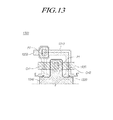
- the transistor 1100 according to the fourth exemplary embodiment is a double bent gate type transistor in which the third electrode unit 1130 is bent at two positions in a " " shape.
- the third voltage V3 is applied to one point P1 of the bent points of the third electrode unit 1130 of the transistor 1100 according to the fourth exemplary embodiment of the present invention.
- the first electrode unit 1110 is formed to be interposed between the opposite ends of the second electrode unit 1120, and one or two semiconductor layers 1140 in a " " shape may be formed over one end of the second electrode unit 1120, the interposed portion of the first electrode unit, and the other end of the second electrode unit 1120.
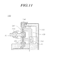
- the third electrode unit 1130 corresponding to a gate electrode is formed on a substrate 1210.
- the semiconductor layer 1140 made of amorphous silicon (a-Si:H) or low temperature polycrystalline silicon (LTPS) is formed on a gate insulation layer 1220.
- a-Si:H amorphous silicon
- LTPS low temperature polycrystalline silicon
- the first electrode unit 1110 and the second electrode unit 1120 are formed. At this time, the first electrode unit 1110 and the second electrode unit 1120 are connected with the semiconductor layer 1140 through a contact hole.
- the second electrode unit 1320 is formed with a second electrode body 1420 and two second electrode protrusions 1421 and 1422 that function as the two first electrodes and protrude from the second electrode body 1420.
- the first electrode unit, the second electrode unit, and the two channels CH1 and CH2 are formed together in the single body 1400.
- the metallic oxide semiconductor material may be, for example, a zinc-oxide based material.
- the metallic oxide semiconductor material may also be a zinc-oxide based material containing indium.
- the metallic oxide semiconductor material may be, for example, Indium Gallium Zinc Oxide (IGZO), Zinc Tin Oxide (ZTO), and Indium Zinc Oxide (IZO).
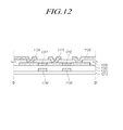
- a semiconductor layer 1520 is formed on a substrate 1510.
- the semiconductor layer 1520 corresponds to the single body 1400 of FIG. 14 .
- the two channels CH1 and CH2 of the transistor 1600 according to the sixth exemplary embodiment are formed in a layer which is different from the layer where the first electrode unit 1610 and the second electrode unit 1620 are formed and may be formed in a semiconductor layer made of amorphous silicon (a-Si:H) or low temperature polycrystalline silicon (LTPS).
- a-Si:H amorphous silicon
- LTPS low temperature polycrystalline silicon
- the at least one pixel among the plurality of pixels defined in the display panel 110 of the display device 100 has a pixel defect and has been repaired
- the at least one pixel among the plurality of pixels will include a transistor according to one or more embodiments among the six embodiments of the present invention that has been repaired.
- FIGs. 19a to 19f are plan views of repaired transistors 300, 600, 800, 1100, 1300, and 1600 according to the first to sixth embodiments.
- FIGs. 20 and 21 are an equivalent circuit diagram of a pixel in which a transistor structure according to one embodiment of the present invention is applied to the driving transistor DT and a cross-sectional view of the organic light-emitting display device, respectively.
- the first electrode unit 310 and the second electrode unit 320 of the driving transistor DT are formed together with the source electrode and the drain electrode of the first transistor T1.
- the two channels CH1 and CH2 of the driving transistor DT are formed together with the channel of the first transistor.
- FIGs. 22a and 22b are plan views of a liquid crystal display device before and after a transistor structure according to exemplary embodiments is applied thereto.
- each pixel is defined by a data line and a gate line, and at least one transistor TR is disposed in each pixel.
Landscapes
- Physics & Mathematics (AREA)
- Engineering & Computer Science (AREA)
- General Physics & Mathematics (AREA)
- Nonlinear Science (AREA)
- Chemical & Material Sciences (AREA)
- Crystallography & Structural Chemistry (AREA)
- Microelectronics & Electronic Packaging (AREA)
- Theoretical Computer Science (AREA)
- Mathematical Physics (AREA)
- Optics & Photonics (AREA)
- Computer Hardware Design (AREA)
- Thin Film Transistor (AREA)
- Devices For Indicating Variable Information By Combining Individual Elements (AREA)
- Liquid Crystal (AREA)
- Electroluminescent Light Sources (AREA)
Applications Claiming Priority (1)
| Application Number | Priority Date | Filing Date | Title |
|---|---|---|---|
| KR1020130165291A KR102195180B1 (ko) | 2013-12-27 | 2013-12-27 | 리던던시 트랜지스터 구조를 갖는 표시장치 |
Publications (2)
| Publication Number | Publication Date |
|---|---|
| EP2889682A1 true EP2889682A1 (de) | 2015-07-01 |
| EP2889682B1 EP2889682B1 (de) | 2016-11-02 |
Family
ID=51022753
Family Applications (1)
| Application Number | Title | Priority Date | Filing Date |
|---|---|---|---|
| EP14174907.7A Active EP2889682B1 (de) | 2013-12-27 | 2014-06-30 | Anzeigevorrichtung mit redundanter Transistorstruktur |
Country Status (6)
| Country | Link |
|---|---|
| US (1) | US9147699B2 (de) |
| EP (1) | EP2889682B1 (de) |
| KR (1) | KR102195180B1 (de) |
| CN (1) | CN104751760B (de) |
| DE (1) | DE102014116179A1 (de) |
| TW (1) | TWI651576B (de) |
Families Citing this family (11)
| Publication number | Priority date | Publication date | Assignee | Title |
|---|---|---|---|---|
| CN105047163A (zh) * | 2015-08-27 | 2015-11-11 | 京东方科技集团股份有限公司 | 栅极驱动电路结构及其修复方法、阵列基板 |
| KR102443832B1 (ko) * | 2015-12-31 | 2022-09-19 | 엘지디스플레이 주식회사 | 유기발광표시패널 및 이를 포함하는 유기발광표시장치 |
| CN110337687A (zh) * | 2017-02-10 | 2019-10-15 | L3技术公司 | 具有双晶体管像素单元的容错lcd显示器 |
| KR102263122B1 (ko) * | 2017-10-19 | 2021-06-09 | 삼성디스플레이 주식회사 | 트랜지스터 표시판 |
| CN107742648A (zh) | 2017-10-27 | 2018-02-27 | 京东方科技集团股份有限公司 | 薄膜晶体管、阵列基板及其制造方法和显示装置 |
| CN108594553B (zh) * | 2018-05-08 | 2022-09-09 | 京东方科技集团股份有限公司 | 一种阵列基板、其修复方法及显示装置 |
| CN111933582B (zh) * | 2020-08-17 | 2024-06-11 | 京东方科技集团股份有限公司 | 像素暗点化处理方法、阵列基板及其制作方法及显示装置 |
| CN114446187B (zh) * | 2020-11-03 | 2023-06-27 | 成都辰显光电有限公司 | 驱动背板、显示面板及其制备方法 |
| KR20220091697A (ko) * | 2020-12-23 | 2022-07-01 | 삼성디스플레이 주식회사 | 표시 장치 및 그 리페어 방법 |
| KR20230103739A (ko) * | 2021-12-31 | 2023-07-07 | 엘지디스플레이 주식회사 | 발광 표시 장치 이의 수리 방법 |
| CN117456913A (zh) * | 2022-07-13 | 2024-01-26 | 北京京东方技术开发有限公司 | 半导体基板及其驱动方法、半导体显示装置 |
Citations (3)
| Publication number | Priority date | Publication date | Assignee | Title |
|---|---|---|---|---|
| JPH07199221A (ja) * | 1993-12-28 | 1995-08-04 | Toshiba Corp | 液晶表示装置 |
| JPH10107150A (ja) * | 1996-10-01 | 1998-04-24 | Sharp Corp | 半導体装置およびそれを備えた画像表示装置 |
| JPH1197701A (ja) * | 1997-09-18 | 1999-04-09 | Seiko Epson Corp | 薄膜トランジスタ、その製造方法及び液晶表示装置 |
Family Cites Families (7)
| Publication number | Priority date | Publication date | Assignee | Title |
|---|---|---|---|---|
| JP3437747B2 (ja) * | 1997-09-19 | 2003-08-18 | 株式会社東芝 | インクジェット記録装置 |
| US6657698B1 (en) * | 1999-08-06 | 2003-12-02 | Rainbow Displays, Inc. | Design features optimized for tiled flat-panel displays |
| US6456354B2 (en) * | 1999-08-06 | 2002-09-24 | Rainbow Displays, Inc. | Design features optimized for tiled flat-panel displays |
| TWI223569B (en) * | 2002-03-20 | 2004-11-01 | Sanyo Electric Co | Method for reducing light quantity of organic EL panel and organic EL panel |
| US8619225B2 (en) * | 2007-03-28 | 2013-12-31 | Japan Display West Inc. | Liquid crystal device with pixel electrode under the common electrode and thinner than drain electrode, method of manufacturing liquid crystal device, and electronic apparatus |
| TWI459587B (zh) * | 2012-02-02 | 2014-11-01 | Chunghwa Picture Tubes Ltd | 主動式發光元件 |
| CN102998869B (zh) * | 2012-12-14 | 2015-11-11 | 京东方科技集团股份有限公司 | 薄膜晶体管阵列基板及其制作方法、显示装置 |
-
2013
- 2013-12-27 KR KR1020130165291A patent/KR102195180B1/ko active Active
-
2014
- 2014-06-30 EP EP14174907.7A patent/EP2889682B1/de active Active
- 2014-07-23 CN CN201410354284.4A patent/CN104751760B/zh active Active
- 2014-09-03 US US14/476,431 patent/US9147699B2/en active Active
- 2014-11-06 DE DE102014116179.3A patent/DE102014116179A1/de not_active Ceased
- 2014-11-26 TW TW103141068A patent/TWI651576B/zh active
Patent Citations (3)
| Publication number | Priority date | Publication date | Assignee | Title |
|---|---|---|---|---|
| JPH07199221A (ja) * | 1993-12-28 | 1995-08-04 | Toshiba Corp | 液晶表示装置 |
| JPH10107150A (ja) * | 1996-10-01 | 1998-04-24 | Sharp Corp | 半導体装置およびそれを備えた画像表示装置 |
| JPH1197701A (ja) * | 1997-09-18 | 1999-04-09 | Seiko Epson Corp | 薄膜トランジスタ、その製造方法及び液晶表示装置 |
Also Published As
| Publication number | Publication date |
|---|---|
| EP2889682B1 (de) | 2016-11-02 |
| US9147699B2 (en) | 2015-09-29 |
| TW201525597A (zh) | 2015-07-01 |
| TWI651576B (zh) | 2019-02-21 |
| KR102195180B1 (ko) | 2020-12-28 |
| CN104751760B (zh) | 2017-11-21 |
| CN104751760A (zh) | 2015-07-01 |
| DE102014116179A1 (de) | 2015-07-02 |
| KR20150077518A (ko) | 2015-07-08 |
| US20150187804A1 (en) | 2015-07-02 |
Similar Documents
| Publication | Publication Date | Title |
|---|---|---|
| EP2889682B1 (de) | Anzeigevorrichtung mit redundanter Transistorstruktur | |
| US11210975B2 (en) | Transparent display device and transparent display panel | |
| US9632378B2 (en) | Display device | |
| KR102702938B1 (ko) | 멀티 타입의 박막 트랜지스터를 포함하는 유기발광 표시장치 | |
| CN101946327B (zh) | Tft、移位寄存器、扫描信号线驱动电路、开关电路和显示装置 | |
| EP3330952B1 (de) | Organische lichtemittierende anzeigevorrichtung und verfahren für deren reparatur | |
| US8102481B2 (en) | Array substrate of liquid crystal display | |
| US9859496B2 (en) | Organic light-emitting diode display device having an extension line crossing second signal lines | |
| US10497309B2 (en) | Organic light emitting diode display and method for repairing the same | |
| US10403209B2 (en) | Array substrate, electrical aging method, display device and manufacturing method thereof | |
| CN104319354B (zh) | 一种管脚绑定结构及显示面板 | |
| WO2011096125A1 (ja) | 表示装置 | |
| CN205355054U (zh) | 显示器薄膜晶体管结构及显示器 | |
| US10199401B2 (en) | Array substrate and method for maintaining the same, display panel and display device | |
| US10141349B2 (en) | Thin-film transistor array, fabrication method therefor, image display device and display method | |
| CN203950504U (zh) | 有源矩阵型显示装置 | |
| US11929027B2 (en) | Display device | |
| DE102023134405A1 (de) | Anzeigevorrichtung | |
| KR102182880B1 (ko) | 리페어 구조를 갖는 표시장치 및 표시패널 | |
| US20180040508A1 (en) | Tft structure and repair method thereof, goa circuit | |
| US12484428B2 (en) | Display device | |
| US12154894B2 (en) | Display device with divided capacitors | |
| US9553137B2 (en) | Display device | |
| DE102024120109A1 (de) | Anzeigevorrichtung | |
| DE102024122528A1 (de) | Anzeigevorrichtung |
Legal Events
| Date | Code | Title | Description |
|---|---|---|---|
| PUAI | Public reference made under article 153(3) epc to a published international application that has entered the european phase |
Free format text: ORIGINAL CODE: 0009012 |
|
| 17P | Request for examination filed |
Effective date: 20140630 |
|
| AK | Designated contracting states |
Kind code of ref document: A1 Designated state(s): AL AT BE BG CH CY CZ DE DK EE ES FI FR GB GR HR HU IE IS IT LI LT LU LV MC MK MT NL NO PL PT RO RS SE SI SK SM TR |
|
| AX | Request for extension of the european patent |
Extension state: BA ME |
|
| R17P | Request for examination filed (corrected) |
Effective date: 20151229 |
|
| RBV | Designated contracting states (corrected) |
Designated state(s): AL AT BE BG CH CY CZ DE DK EE ES FI FR GB GR HR HU IE IS IT LI LT LU LV MC MK MT NL NO PL PT RO RS SE SI SK SM TR |
|
| GRAP | Despatch of communication of intention to grant a patent |
Free format text: ORIGINAL CODE: EPIDOSNIGR1 |
|
| RIC1 | Information provided on ipc code assigned before grant |
Ipc: G02F 1/1362 20060101AFI20160425BHEP Ipc: H01L 27/32 20060101ALI20160425BHEP |
|
| INTG | Intention to grant announced |
Effective date: 20160601 |
|
| RAP1 | Party data changed (applicant data changed or rights of an application transferred) |
Owner name: LG DISPLAY CO., LTD. |
|
| GRAS | Grant fee paid |
Free format text: ORIGINAL CODE: EPIDOSNIGR3 |
|
| GRAA | (expected) grant |
Free format text: ORIGINAL CODE: 0009210 |
|
| AK | Designated contracting states |
Kind code of ref document: B1 Designated state(s): AL AT BE BG CH CY CZ DE DK EE ES FI FR GB GR HR HU IE IS IT LI LT LU LV MC MK MT NL NO PL PT RO RS SE SI SK SM TR |
|
| REG | Reference to a national code |
Ref country code: GB Ref legal event code: FG4D |
|
| REG | Reference to a national code |
Ref country code: AT Ref legal event code: REF Ref document number: 842416 Country of ref document: AT Kind code of ref document: T Effective date: 20161115 Ref country code: CH Ref legal event code: EP |
|
| REG | Reference to a national code |
Ref country code: IE Ref legal event code: FG4D |
|
| REG | Reference to a national code |
Ref country code: DE Ref legal event code: R096 Ref document number: 602014004575 Country of ref document: DE |
|
| PG25 | Lapsed in a contracting state [announced via postgrant information from national office to epo] |
Ref country code: LV Free format text: LAPSE BECAUSE OF FAILURE TO SUBMIT A TRANSLATION OF THE DESCRIPTION OR TO PAY THE FEE WITHIN THE PRESCRIBED TIME-LIMIT Effective date: 20161102 |
|
| REG | Reference to a national code |
Ref country code: NL Ref legal event code: MP Effective date: 20161102 |
|
| REG | Reference to a national code |
Ref country code: LT Ref legal event code: MG4D |
|
| REG | Reference to a national code |
Ref country code: AT Ref legal event code: MK05 Ref document number: 842416 Country of ref document: AT Kind code of ref document: T Effective date: 20161102 |
|
| PG25 | Lapsed in a contracting state [announced via postgrant information from national office to epo] |
Ref country code: NL Free format text: LAPSE BECAUSE OF FAILURE TO SUBMIT A TRANSLATION OF THE DESCRIPTION OR TO PAY THE FEE WITHIN THE PRESCRIBED TIME-LIMIT Effective date: 20161102 Ref country code: LT Free format text: LAPSE BECAUSE OF FAILURE TO SUBMIT A TRANSLATION OF THE DESCRIPTION OR TO PAY THE FEE WITHIN THE PRESCRIBED TIME-LIMIT Effective date: 20161102 Ref country code: NO Free format text: LAPSE BECAUSE OF FAILURE TO SUBMIT A TRANSLATION OF THE DESCRIPTION OR TO PAY THE FEE WITHIN THE PRESCRIBED TIME-LIMIT Effective date: 20170202 Ref country code: SE Free format text: LAPSE BECAUSE OF FAILURE TO SUBMIT A TRANSLATION OF THE DESCRIPTION OR TO PAY THE FEE WITHIN THE PRESCRIBED TIME-LIMIT Effective date: 20161102 Ref country code: GR Free format text: LAPSE BECAUSE OF FAILURE TO SUBMIT A TRANSLATION OF THE DESCRIPTION OR TO PAY THE FEE WITHIN THE PRESCRIBED TIME-LIMIT Effective date: 20170203 |
|
| PG25 | Lapsed in a contracting state [announced via postgrant information from national office to epo] |
Ref country code: HR Free format text: LAPSE BECAUSE OF FAILURE TO SUBMIT A TRANSLATION OF THE DESCRIPTION OR TO PAY THE FEE WITHIN THE PRESCRIBED TIME-LIMIT Effective date: 20161102 Ref country code: PL Free format text: LAPSE BECAUSE OF FAILURE TO SUBMIT A TRANSLATION OF THE DESCRIPTION OR TO PAY THE FEE WITHIN THE PRESCRIBED TIME-LIMIT Effective date: 20161102 Ref country code: PT Free format text: LAPSE BECAUSE OF FAILURE TO SUBMIT A TRANSLATION OF THE DESCRIPTION OR TO PAY THE FEE WITHIN THE PRESCRIBED TIME-LIMIT Effective date: 20170302 Ref country code: AT Free format text: LAPSE BECAUSE OF FAILURE TO SUBMIT A TRANSLATION OF THE DESCRIPTION OR TO PAY THE FEE WITHIN THE PRESCRIBED TIME-LIMIT Effective date: 20161102 Ref country code: IS Free format text: LAPSE BECAUSE OF FAILURE TO SUBMIT A TRANSLATION OF THE DESCRIPTION OR TO PAY THE FEE WITHIN THE PRESCRIBED TIME-LIMIT Effective date: 20170302 Ref country code: RS Free format text: LAPSE BECAUSE OF FAILURE TO SUBMIT A TRANSLATION OF THE DESCRIPTION OR TO PAY THE FEE WITHIN THE PRESCRIBED TIME-LIMIT Effective date: 20161102 Ref country code: ES Free format text: LAPSE BECAUSE OF FAILURE TO SUBMIT A TRANSLATION OF THE DESCRIPTION OR TO PAY THE FEE WITHIN THE PRESCRIBED TIME-LIMIT Effective date: 20161102 Ref country code: FI Free format text: LAPSE BECAUSE OF FAILURE TO SUBMIT A TRANSLATION OF THE DESCRIPTION OR TO PAY THE FEE WITHIN THE PRESCRIBED TIME-LIMIT Effective date: 20161102 |
|
| REG | Reference to a national code |
Ref country code: FR Ref legal event code: PLFP Year of fee payment: 4 |
|
| PG25 | Lapsed in a contracting state [announced via postgrant information from national office to epo] |
Ref country code: SK Free format text: LAPSE BECAUSE OF FAILURE TO SUBMIT A TRANSLATION OF THE DESCRIPTION OR TO PAY THE FEE WITHIN THE PRESCRIBED TIME-LIMIT Effective date: 20161102 Ref country code: EE Free format text: LAPSE BECAUSE OF FAILURE TO SUBMIT A TRANSLATION OF THE DESCRIPTION OR TO PAY THE FEE WITHIN THE PRESCRIBED TIME-LIMIT Effective date: 20161102 Ref country code: DK Free format text: LAPSE BECAUSE OF FAILURE TO SUBMIT A TRANSLATION OF THE DESCRIPTION OR TO PAY THE FEE WITHIN THE PRESCRIBED TIME-LIMIT Effective date: 20161102 Ref country code: RO Free format text: LAPSE BECAUSE OF FAILURE TO SUBMIT A TRANSLATION OF THE DESCRIPTION OR TO PAY THE FEE WITHIN THE PRESCRIBED TIME-LIMIT Effective date: 20161102 Ref country code: CZ Free format text: LAPSE BECAUSE OF FAILURE TO SUBMIT A TRANSLATION OF THE DESCRIPTION OR TO PAY THE FEE WITHIN THE PRESCRIBED TIME-LIMIT Effective date: 20161102 |
|
| REG | Reference to a national code |
Ref country code: DE Ref legal event code: R097 Ref document number: 602014004575 Country of ref document: DE |
|
| PG25 | Lapsed in a contracting state [announced via postgrant information from national office to epo] |
Ref country code: IT Free format text: LAPSE BECAUSE OF FAILURE TO SUBMIT A TRANSLATION OF THE DESCRIPTION OR TO PAY THE FEE WITHIN THE PRESCRIBED TIME-LIMIT Effective date: 20161102 Ref country code: SM Free format text: LAPSE BECAUSE OF FAILURE TO SUBMIT A TRANSLATION OF THE DESCRIPTION OR TO PAY THE FEE WITHIN THE PRESCRIBED TIME-LIMIT Effective date: 20161102 Ref country code: BG Free format text: LAPSE BECAUSE OF FAILURE TO SUBMIT A TRANSLATION OF THE DESCRIPTION OR TO PAY THE FEE WITHIN THE PRESCRIBED TIME-LIMIT Effective date: 20170202 Ref country code: BE Free format text: LAPSE BECAUSE OF FAILURE TO SUBMIT A TRANSLATION OF THE DESCRIPTION OR TO PAY THE FEE WITHIN THE PRESCRIBED TIME-LIMIT Effective date: 20161102 |
|
| PLBE | No opposition filed within time limit |
Free format text: ORIGINAL CODE: 0009261 |
|
| STAA | Information on the status of an ep patent application or granted ep patent |
Free format text: STATUS: NO OPPOSITION FILED WITHIN TIME LIMIT |
|
| 26N | No opposition filed |
Effective date: 20170803 |
|
| PG25 | Lapsed in a contracting state [announced via postgrant information from national office to epo] |
Ref country code: SI Free format text: LAPSE BECAUSE OF FAILURE TO SUBMIT A TRANSLATION OF THE DESCRIPTION OR TO PAY THE FEE WITHIN THE PRESCRIBED TIME-LIMIT Effective date: 20161102 |
|
| PG25 | Lapsed in a contracting state [announced via postgrant information from national office to epo] |
Ref country code: MC Free format text: LAPSE BECAUSE OF FAILURE TO SUBMIT A TRANSLATION OF THE DESCRIPTION OR TO PAY THE FEE WITHIN THE PRESCRIBED TIME-LIMIT Effective date: 20161102 |
|
| REG | Reference to a national code |
Ref country code: CH Ref legal event code: PL |
|
| REG | Reference to a national code |
Ref country code: IE Ref legal event code: MM4A |
|
| PG25 | Lapsed in a contracting state [announced via postgrant information from national office to epo] |
Ref country code: LU Free format text: LAPSE BECAUSE OF NON-PAYMENT OF DUE FEES Effective date: 20170630 Ref country code: IE Free format text: LAPSE BECAUSE OF NON-PAYMENT OF DUE FEES Effective date: 20170630 Ref country code: LI Free format text: LAPSE BECAUSE OF NON-PAYMENT OF DUE FEES Effective date: 20170630 Ref country code: CH Free format text: LAPSE BECAUSE OF NON-PAYMENT OF DUE FEES Effective date: 20170630 |
|
| REG | Reference to a national code |
Ref country code: FR Ref legal event code: PLFP Year of fee payment: 5 |
|
| PG25 | Lapsed in a contracting state [announced via postgrant information from national office to epo] |
Ref country code: MT Free format text: LAPSE BECAUSE OF NON-PAYMENT OF DUE FEES Effective date: 20170630 |
|
| PG25 | Lapsed in a contracting state [announced via postgrant information from national office to epo] |
Ref country code: HU Free format text: LAPSE BECAUSE OF FAILURE TO SUBMIT A TRANSLATION OF THE DESCRIPTION OR TO PAY THE FEE WITHIN THE PRESCRIBED TIME-LIMIT; INVALID AB INITIO Effective date: 20140630 |
|
| PG25 | Lapsed in a contracting state [announced via postgrant information from national office to epo] |
Ref country code: CY Free format text: LAPSE BECAUSE OF FAILURE TO SUBMIT A TRANSLATION OF THE DESCRIPTION OR TO PAY THE FEE WITHIN THE PRESCRIBED TIME-LIMIT Effective date: 20161102 |
|
| PG25 | Lapsed in a contracting state [announced via postgrant information from national office to epo] |
Ref country code: MK Free format text: LAPSE BECAUSE OF FAILURE TO SUBMIT A TRANSLATION OF THE DESCRIPTION OR TO PAY THE FEE WITHIN THE PRESCRIBED TIME-LIMIT Effective date: 20161102 |
|
| PG25 | Lapsed in a contracting state [announced via postgrant information from national office to epo] |
Ref country code: TR Free format text: LAPSE BECAUSE OF FAILURE TO SUBMIT A TRANSLATION OF THE DESCRIPTION OR TO PAY THE FEE WITHIN THE PRESCRIBED TIME-LIMIT Effective date: 20161102 |
|
| PG25 | Lapsed in a contracting state [announced via postgrant information from national office to epo] |
Ref country code: AL Free format text: LAPSE BECAUSE OF FAILURE TO SUBMIT A TRANSLATION OF THE DESCRIPTION OR TO PAY THE FEE WITHIN THE PRESCRIBED TIME-LIMIT Effective date: 20161102 |
|
| PGFP | Annual fee paid to national office [announced via postgrant information from national office to epo] |
Ref country code: DE Payment date: 20250422 Year of fee payment: 12 |
|
| PGFP | Annual fee paid to national office [announced via postgrant information from national office to epo] |
Ref country code: GB Payment date: 20250422 Year of fee payment: 12 |
|
| PGFP | Annual fee paid to national office [announced via postgrant information from national office to epo] |
Ref country code: FR Payment date: 20250422 Year of fee payment: 12 |