US9147699B2 - Display device with redundant transistor structure - Google Patents
Display device with redundant transistor structure Download PDFInfo
- Publication number
- US9147699B2 US9147699B2 US14/476,431 US201414476431A US9147699B2 US 9147699 B2 US9147699 B2 US 9147699B2 US 201414476431 A US201414476431 A US 201414476431A US 9147699 B2 US9147699 B2 US 9147699B2
- Authority
- US
- United States
- Prior art keywords
- electrode unit
- electrode
- transistor
- display device
- shape
- Prior art date
- Legal status (The legal status is an assumption and is not a legal conclusion. Google has not performed a legal analysis and makes no representation as to the accuracy of the status listed.)
- Active
Links
Images


Classifications
-
- H01L27/124—
-
- G—PHYSICS
- G02—OPTICS
- G02F—OPTICAL DEVICES OR ARRANGEMENTS FOR THE CONTROL OF LIGHT BY MODIFICATION OF THE OPTICAL PROPERTIES OF THE MEDIA OF THE ELEMENTS INVOLVED THEREIN; NON-LINEAR OPTICS; FREQUENCY-CHANGING OF LIGHT; OPTICAL LOGIC ELEMENTS; OPTICAL ANALOGUE/DIGITAL CONVERTERS
- G02F1/00—Devices or arrangements for the control of the intensity, colour, phase, polarisation or direction of light arriving from an independent light source, e.g. switching, gating or modulating; Non-linear optics
- G02F1/01—Devices or arrangements for the control of the intensity, colour, phase, polarisation or direction of light arriving from an independent light source, e.g. switching, gating or modulating; Non-linear optics for the control of the intensity, phase, polarisation or colour
- G02F1/13—Devices or arrangements for the control of the intensity, colour, phase, polarisation or direction of light arriving from an independent light source, e.g. switching, gating or modulating; Non-linear optics for the control of the intensity, phase, polarisation or colour based on liquid crystals, e.g. single liquid crystal display cells
- G02F1/133—Constructional arrangements; Operation of liquid crystal cells; Circuit arrangements
- G02F1/136—Liquid crystal cells structurally associated with a semi-conducting layer or substrate, e.g. cells forming part of an integrated circuit
- G02F1/1362—Active matrix addressed cells
- G02F1/136259—Repairing; Defects
-
- G—PHYSICS
- G09—EDUCATION; CRYPTOGRAPHY; DISPLAY; ADVERTISING; SEALS
- G09G—ARRANGEMENTS OR CIRCUITS FOR CONTROL OF INDICATING DEVICES USING STATIC MEANS TO PRESENT VARIABLE INFORMATION
- G09G3/00—Control arrangements or circuits, of interest only in connection with visual indicators other than cathode-ray tubes
- G09G3/20—Control arrangements or circuits, of interest only in connection with visual indicators other than cathode-ray tubes for presentation of an assembly of a number of characters, e.g. a page, by composing the assembly by combination of individual elements arranged in a matrix no fixed position being assigned to or needed to be assigned to the individual characters or partial characters
-
- H—ELECTRICITY
- H10—SEMICONDUCTOR DEVICES; ELECTRIC SOLID-STATE DEVICES NOT OTHERWISE PROVIDED FOR
- H10D—INORGANIC ELECTRIC SEMICONDUCTOR DEVICES
- H10D86/00—Integrated devices formed in or on insulating or conducting substrates, e.g. formed in silicon-on-insulator [SOI] substrates or on stainless steel or glass substrates
- H10D86/40—Integrated devices formed in or on insulating or conducting substrates, e.g. formed in silicon-on-insulator [SOI] substrates or on stainless steel or glass substrates characterised by multiple TFTs
- H10D86/60—Integrated devices formed in or on insulating or conducting substrates, e.g. formed in silicon-on-insulator [SOI] substrates or on stainless steel or glass substrates characterised by multiple TFTs wherein the TFTs are in active matrices
-
- G—PHYSICS
- G09—EDUCATION; CRYPTOGRAPHY; DISPLAY; ADVERTISING; SEALS
- G09F—DISPLAYING; ADVERTISING; SIGNS; LABELS OR NAME-PLATES; SEALS
- G09F9/00—Indicating arrangements for variable information in which the information is built-up on a support by selection or combination of individual elements
- G09F9/30—Indicating arrangements for variable information in which the information is built-up on a support by selection or combination of individual elements in which the desired character or characters are formed by combining individual elements
-
- H01L27/1222—
-
- H01L27/1225—
-
- H01L27/1255—
-
- H01L29/41733—
-
- H01L29/42384—
-
- H01L29/78663—
-
- H01L29/78672—
-
- H01L29/7869—
-
- H—ELECTRICITY
- H10—SEMICONDUCTOR DEVICES; ELECTRIC SOLID-STATE DEVICES NOT OTHERWISE PROVIDED FOR
- H10D—INORGANIC ELECTRIC SEMICONDUCTOR DEVICES
- H10D30/00—Field-effect transistors [FET]
- H10D30/60—Insulated-gate field-effect transistors [IGFET]
- H10D30/67—Thin-film transistors [TFT]
- H10D30/6729—Thin-film transistors [TFT] characterised by the electrodes
- H10D30/673—Thin-film transistors [TFT] characterised by the electrodes characterised by the shapes, relative sizes or dispositions of the gate electrodes
-
- H—ELECTRICITY
- H10—SEMICONDUCTOR DEVICES; ELECTRIC SOLID-STATE DEVICES NOT OTHERWISE PROVIDED FOR
- H10D—INORGANIC ELECTRIC SEMICONDUCTOR DEVICES
- H10D30/00—Field-effect transistors [FET]
- H10D30/60—Insulated-gate field-effect transistors [IGFET]
- H10D30/67—Thin-film transistors [TFT]
- H10D30/674—Thin-film transistors [TFT] characterised by the active materials
- H10D30/6741—Group IV materials, e.g. germanium or silicon carbide
- H10D30/6743—Silicon
- H10D30/6745—Polycrystalline or microcrystalline silicon
-
- H—ELECTRICITY
- H10—SEMICONDUCTOR DEVICES; ELECTRIC SOLID-STATE DEVICES NOT OTHERWISE PROVIDED FOR
- H10D—INORGANIC ELECTRIC SEMICONDUCTOR DEVICES
- H10D30/00—Field-effect transistors [FET]
- H10D30/60—Insulated-gate field-effect transistors [IGFET]
- H10D30/67—Thin-film transistors [TFT]
- H10D30/674—Thin-film transistors [TFT] characterised by the active materials
- H10D30/6741—Group IV materials, e.g. germanium or silicon carbide
- H10D30/6743—Silicon
- H10D30/6746—Amorphous silicon
-
- H—ELECTRICITY
- H10—SEMICONDUCTOR DEVICES; ELECTRIC SOLID-STATE DEVICES NOT OTHERWISE PROVIDED FOR
- H10D—INORGANIC ELECTRIC SEMICONDUCTOR DEVICES
- H10D30/00—Field-effect transistors [FET]
- H10D30/60—Insulated-gate field-effect transistors [IGFET]
- H10D30/67—Thin-film transistors [TFT]
- H10D30/674—Thin-film transistors [TFT] characterised by the active materials
- H10D30/6755—Oxide semiconductors, e.g. zinc oxide, copper aluminium oxide or cadmium stannate
-
- H—ELECTRICITY
- H10—SEMICONDUCTOR DEVICES; ELECTRIC SOLID-STATE DEVICES NOT OTHERWISE PROVIDED FOR
- H10D—INORGANIC ELECTRIC SEMICONDUCTOR DEVICES
- H10D86/00—Integrated devices formed in or on insulating or conducting substrates, e.g. formed in silicon-on-insulator [SOI] substrates or on stainless steel or glass substrates
- H10D86/40—Integrated devices formed in or on insulating or conducting substrates, e.g. formed in silicon-on-insulator [SOI] substrates or on stainless steel or glass substrates characterised by multiple TFTs
- H10D86/421—Integrated devices formed in or on insulating or conducting substrates, e.g. formed in silicon-on-insulator [SOI] substrates or on stainless steel or glass substrates characterised by multiple TFTs having a particular composition, shape or crystalline structure of the active layer
- H10D86/423—Integrated devices formed in or on insulating or conducting substrates, e.g. formed in silicon-on-insulator [SOI] substrates or on stainless steel or glass substrates characterised by multiple TFTs having a particular composition, shape or crystalline structure of the active layer comprising semiconductor materials not belonging to the Group IV, e.g. InGaZnO
-
- H—ELECTRICITY
- H10—SEMICONDUCTOR DEVICES; ELECTRIC SOLID-STATE DEVICES NOT OTHERWISE PROVIDED FOR
- H10D—INORGANIC ELECTRIC SEMICONDUCTOR DEVICES
- H10D86/00—Integrated devices formed in or on insulating or conducting substrates, e.g. formed in silicon-on-insulator [SOI] substrates or on stainless steel or glass substrates
- H10D86/40—Integrated devices formed in or on insulating or conducting substrates, e.g. formed in silicon-on-insulator [SOI] substrates or on stainless steel or glass substrates characterised by multiple TFTs
- H10D86/441—Interconnections, e.g. scanning lines
-
- H—ELECTRICITY
- H10—SEMICONDUCTOR DEVICES; ELECTRIC SOLID-STATE DEVICES NOT OTHERWISE PROVIDED FOR
- H10D—INORGANIC ELECTRIC SEMICONDUCTOR DEVICES
- H10D86/00—Integrated devices formed in or on insulating or conducting substrates, e.g. formed in silicon-on-insulator [SOI] substrates or on stainless steel or glass substrates
- H10D86/40—Integrated devices formed in or on insulating or conducting substrates, e.g. formed in silicon-on-insulator [SOI] substrates or on stainless steel or glass substrates characterised by multiple TFTs
- H10D86/481—Integrated devices formed in or on insulating or conducting substrates, e.g. formed in silicon-on-insulator [SOI] substrates or on stainless steel or glass substrates characterised by multiple TFTs integrated with passive devices, e.g. auxiliary capacitors
-
- G—PHYSICS
- G02—OPTICS
- G02F—OPTICAL DEVICES OR ARRANGEMENTS FOR THE CONTROL OF LIGHT BY MODIFICATION OF THE OPTICAL PROPERTIES OF THE MEDIA OF THE ELEMENTS INVOLVED THEREIN; NON-LINEAR OPTICS; FREQUENCY-CHANGING OF LIGHT; OPTICAL LOGIC ELEMENTS; OPTICAL ANALOGUE/DIGITAL CONVERTERS
- G02F1/00—Devices or arrangements for the control of the intensity, colour, phase, polarisation or direction of light arriving from an independent light source, e.g. switching, gating or modulating; Non-linear optics
- G02F1/01—Devices or arrangements for the control of the intensity, colour, phase, polarisation or direction of light arriving from an independent light source, e.g. switching, gating or modulating; Non-linear optics for the control of the intensity, phase, polarisation or colour
- G02F1/13—Devices or arrangements for the control of the intensity, colour, phase, polarisation or direction of light arriving from an independent light source, e.g. switching, gating or modulating; Non-linear optics for the control of the intensity, phase, polarisation or colour based on liquid crystals, e.g. single liquid crystal display cells
- G02F1/133—Constructional arrangements; Operation of liquid crystal cells; Circuit arrangements
- G02F1/136—Liquid crystal cells structurally associated with a semi-conducting layer or substrate, e.g. cells forming part of an integrated circuit
- G02F1/1362—Active matrix addressed cells
- G02F1/136259—Repairing; Defects
- G02F1/136268—Switch defects
Definitions
- the present invention relates to a display device with a redundant transistor structure.
- a display panel for use in a display device such as a liquid display device or an organic light-emitting display device is, in general, provided with at least one transistor for displaying an image.
- a transistor within each pixel in a display panel is fabricated through a number of processes. During the processes, fine foreign substances, particles, and/or impurities may undesirably be included in the transistors (in particular, in the channel regions). In such an instance, the transistor may be electrically shorted or disconnected and, thus, the transistor may not function normally. This may cause a pixel defect which changes the corresponding pixel into a bright dot or a dark dot.
- Such a pixel defect which changes a pixel into a bright dot or a dark dot may considerably degrade the quality of the image of display devices and reduce the yield of display panel production.
- a repair process has been conventionally performed so as to change a defective pixel that appears as a bright dot, e.g., due to fine foreign substances, rather into a dark dot such that the defective pixel cannot be visually recognized.
- an aspect of the present invention is to provide a display device having a redundant transistor structure that, when a pixel defect occurs due to foreign particles/substances/impurities introduced into a transistor in the display device, enables a repair process such that the corresponding pixel may function as a normal pixel.
- Another aspect of the present invention is to provide a display device having a redundant transistor structure which is capable of enhancing the repair success rate as well as enabling a repair process.
- Yet another aspect of the present invention is to provide a display device having a redundant transistor structure which does not reduce the aperture ratio of the display panel as well as enables a repair process of the display panel.
- Still another aspect of the present invention is to provide a display device including at least one pixel, which can be subjected to a repair process using the redundant transistor structure as described above.
- a display device including: a display panel in which a plurality of data lines and gate lines are formed to define a plurality of pixels; a data drive unit configured to supply a data voltage to the data lines; and a gate drive unit configured to supply a scan signal to the gate lines.
- the display panel is provided with a transistor that includes: a first electrode unit applied with a first voltage and configured to function as two first electrodes; a second electrode unit formed with a second voltage and configured to function as two second electrodes; a third electrode unit applied with a third voltage and configured to function as a common third electrode, the third electrode unit being formed to be bent between the first electrode unit and the second electrode unit; and two channels formed to be spaced apart from each other at points where opposite ends of the third electrode unit are positioned and configured to correspondingly connect the two first electrodes and the two second electrodes, respectively.
- a display device including: a display panel in which a data line and a gate line are formed; a data drive unit configured to supply a data voltage to the data lines; and a gate drive unit configured to supply a scan signal to the gate lines.
- the display panel is provided with a transistor that includes: a first electrode unit applied with a first voltage and configured to function as two first electrodes; a second electrode unit formed with a second voltage and configured to function as two second electrodes; a third electrode unit applied with a third voltage and configured to function as a common third electrode, the third electrode unit being formed in a “ ” shape between the first electrode unit and the second electrode unit; and two channels formed in parallel to each other at points where opposite ends of the third electrode unit are positioned and configured to correspondingly connect the two first electrodes and the two second electrodes, respectively.
- the present invention may provide a display device having a redundant transistor structure which enables a repair process in such a manner that, when a foreign substance exists in a transistor and causes a pixel defect, the corresponding pixel can still function as a normal pixel.
- the present invention may provide a display device having a redundant transistor structure capable of enhancing the repair success rate as well as enabling a repair process.
- the present invention may provide a display device having a redundant transistor structure which does not reduce the aperture ratio of the display panel, while enabling enables a repair process.
- the present invention may provide a display device including at least one pixel that may be subjected to a repair process using a redundant transistor structure.
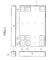
- FIG. 1 is a view illustrating a system configuration of a display device in accordance with embodiments of the present invention
- FIG. 2 is an equivalent circuit diagram of a transistor according to embodiments of the present invention.
- FIG. 3 is a plan view of a transistor according to a first exemplary embodiment
- FIG. 4 is a view illustrating a single body of the transistor TR according to the first exemplary embodiment
- FIG. 5 is a cross-sectional view of the transistor according to the first exemplary embodiment
- FIG. 6 is a plan view of a transistor according to a second exemplary embodiment
- FIG. 7 is a cross-sectional view of the transistor according to the second exemplary embodiment.
- FIG. 8 is a plan view of a transistor according to a third exemplary embodiment
- FIG. 9 is a view illustrating a single body of the transistor according to the third exemplary embodiment.
- FIG. 10 is a cross-sectional view of the transistor according to the third exemplary embodiment.
- FIG. 11 is a plan view of a transistor according to a fourth exemplary embodiment.
- FIG. 12 is a cross-sectional view of the transistor according to the fourth exemplary embodiment.
- FIG. 13 is a plan view of the transistor according to a fifth exemplary embodiment
- FIG. 14 is a view illustrating a single body of the transistor according to the fifth exemplary embodiment.
- FIG. 15 is a cross-sectional view of the transistor according to the fifth exemplary embodiment.
- FIG. 16 is a plan view of a transistor according to a sixth exemplary embodiment.
- FIG. 17 is a cross-sectional view of the transistor according to the sixth exemplary embodiment.
- FIG. 18 is an equivalent circuit diagram of a transistor subjected to a repair process according to embodiments of the present invention.
- FIGS. 19 a to 19 f are plan views of the transistors according to the first to sixth exemplary embodiments which have been subjected to a repair process;
- FIG. 20 is an equivalent circuit diagram of a pixel of an organic light-emitting display device including transistor structures according to embodiments of the present invention.
- FIG. 21 is a cross-sectional view of an organic light-emitting display device including transistor structures according to embodiments of the present invention.
- FIGS. 22 a and 22 b are plan views of a liquid crystal display device before and after transistor structures according to embodiments of the present invention are applied.
- first, second, A, B, (a), (b) or the like may be used herein when describing components of the present invention.
- Each of these terminologies is not used to define an essence, order or sequence of a corresponding component but used merely to distinguish the corresponding component from other component(s).
- a third component may be “interposed” between the first and second components, although the first component may be directly “connected”, “coupled” or “joined” to the second component.
- FIG. 1 illustrates a system configuration of a display device 100 according to one or more embodiments of the present invention.
- the display device 100 includes: a display panel 110 formed with m data lines DL 1 to DLm and n gate lines GL 1 to GLn; a data drive unit 120 configured to supply a data voltage to them data lines DL 1 to DLm; a gate drive unit 130 configured to supply a scan signal to the n gate lines GL 1 to GLn; and a timing controller 140 configured to control a drive timing of the data drive unit 120 and the gate drive unit 130 .
- the above-mentioned gate drive unit 130 may be positioned on only one side of the display panel 110 as illustrated in FIG. 1 or may be divided into two and positioned on both sides of the display panel 110 , depending on the driving type of the gate drive unit 130 .
- the gate drive unit 130 may include a plurality of gate drive integrated circuits.
- the plurality of gate drive integrated circuits may be connected to a bonding pad of the display panel 110 through a Tape Automated Bonding (TAB) method or a Chip On Glass (COG) method, or implemented in a Gate In Panel (GIP) type and directly formed in the display panel 110 .
- TAB Tape Automated Bonding
- COG Chip On Glass
- GIP Gate In Panel
- the plurality of gate drive integrated circuits may be integrated and formed in the display panel 110 .
- the data drive unit 120 may include a plurality of data drive integrated circuits (also referred to as “source driving integrated circuits”).
- the plurality of data drive integrated circuits may be connected to a bonding pad of the display panel by the TAB method or the COG method or directly formed in the display panel 110 .
- the plurality of data drive integrated circuits may be integrated and formed in the display panel 110 .
- the display device 100 may be a Liquid Crystal Display (LCD), or an Organic Light-Emitting Display (OLED) or the like.
- the display device 100 may include at least one transistor in each of a plurality of pixels defined in the display panel 110 regardless of the type of the display device 100 .
- a transistor disposed in a pixel may malfunction or may not function at all when it is shorted or disconnected due to the introduction of undesired foreign substances in the manufacturing process. In that instance, the corresponding pixel typically appears to be a bright dot or a dark dot, thereby becoming a defective pixel.
- the present disclosure proposes various transistor structures that, when a transistor in a pixel is shorted or disconnected due to the introduction of foreign substances in the manufacturing process and, hence, the corresponding pixel becomes a defective pixel, enable a repair process of the defective pixel after which the pixel can function as a normal pixel.
- the repair process may be performed during the panel fabrication process prior to the manufacturing of the product being completed.
- FIG. 2 is an equivalent circuit diagram of a transistor TR according to embodiments of the present invention.
- the transistor TR is a transistor disposed in each of a plurality of pixels defined in a display panel 110 of a display device 100 and has a redundant structure in which a first transistor TR 1 and a second transistor TR 2 are connected in parallel to each other.
- the first transistor TR 1 and the second transistor TR 2 are connected in parallel to each other to perform a switching operation.
- the switching operation in a normal pixel is performed in the same manner that one transistor TR performs its switching operation.
- one of the first transistor TR 1 and the second transistor TR 2 is cut (i.e., disconnected), and only the remaining one performs the switching operation. This will be described in more detail below.
- the transistor TR includes: a first electrode unit E 1 applied with a first voltage V 1 and which configured to function as two first electrodes e 1 and e 1 ′; a second electrode unit E 2 applied with a second voltage V 2 and configured to function as two second electrodes e 2 and e 2 ; a third electrode unit E 3 applied with a third voltage V 3 and configured to function as a common third electrode; and two channels CH 1 and CH 2 configured to correspondingly connect the two first electrodes e 1 and e 1 ′ and the two second electrodes e 2 and e 2 ′, respectively.
- the first transistor TR 1 includes the first electrode e 1 of the first electrode unit E 1 , the second electrode e 2 of the second electrode unit E 2 , the third electrode unit E 3 , and the channel CH 1 that interconnects the first electrode e 1 of the first electrode unit E 1 and the second electrode e 2 of the second electrode unit E 2 .
- the second transistor TR 2 includes the first electrode e 1 ′ of the first electrode unit E 1 , the second electrode e 2 ′ of the second electrode unit E 2 , the third electrode unit E 3 , and the channel CH 2 which interconnects the first electrode e 1 ′ of the first electrode unit E 1 and the second electrode e 2 ′ of the second electrode unit E 2 .
- first transistor TR 1 and the second transistor TR 2 are connected in parallel to each other and function as a single transistor TR.
- the first voltage V 1 is commonly applied to the first and second transistors TR 1 and TR 2 through the first electrode unit E 1 which functions as the two first electrodes e 1 and e 1 ′
- the third voltage V 3 which corresponds to a gate voltage is commonly applied to the first and second transistors TR 1 and TR 2 through the third electrode unit E 3
- the second voltage V 2 is commonly formed in the second electrode unit E 2 which functions as the two second electrodes e 2 and e 2 ′.
- the first electrode unit E 1 and the two first electrodes e 1 and e 1 ′ formed therein may be a source electrode or a drain electrode
- the second electrode unit E 2 and the two second electrodes e 2 and e 2 ′ formed therein may be a drain electrode or a source electrode
- the third electrode unit E 3 may be a gate electrode.
- transistors are illustrated as an N type according to one embodiment. However, this is merely for ease of description, and one skilled in the art would readily appreciate that the transistors may be designed as a P type according to one embodiment.
- transistors TR having a redundant structure in which the first transistor TR 1 and the second transistor TR 2 are connected in parallel to each other will be described in accordance with six exemplary embodiments, which may be differentiated from each other by the gate type and the semiconductor layer material type.
- transistor TR according to a first exemplary embodiment will be described with reference to FIGS. 3 to 5 .
- transistor 300 is a single bent gate type in which a third electrode unit 330 corresponding to a gate electrode is bent at one position, and the semiconductor material is made of a metallic oxide semiconductor material.
- FIG. 3 is a plan view of the transistor 300 according to the first exemplary embodiment
- FIG. 4 illustrates a single body 400 of the transistor 300 according to the first exemplary embodiment in which a first electrode unit 310 , a second electrode unit 320 and channels CH 1 and CH 2 are formed together
- FIG. 5 is a cross-sectional view of the transistor 300 according to the first exemplary embodiment.
- the transistor 300 includes a first electrode unit 310 , a second electrode unit 320 , and a third electrode unit 330 .
- the first electrode unit 310 is applied with a first voltage V 1 and functions as two first electrodes.
- the first electrode unit 310 is formed with a first electrode body 410 and two first electrode protrusions 411 and 412 which function as the two first electrodes and protrude from the first electrode body 410 .
- the second electrode unit 320 receives a second voltage V 2 and functions as two second electrodes.
- the second electrode unit 320 is formed with a second electrode body 420 and two second electrode protrusions 421 and 422 which function as the two second electrodes and protrude from the second electrode body 420 .
- the third electrode unit 330 is applied with a third voltage V 3 and functions as a common third electrode.
- the third electrode unit 330 is formed to be bent between the first electrode unit 310 and the second electrode unit 320 .
- the third electrode unit 330 is bent in a “ ” shape or an “ ” shape.
- a bent point P 1 of the third electrode unit 330 may be a point where the voltage V 3 is applied.
- the third electrode unit 330 may be connected with a first plate 340 of a capacitor through a contact hole, and the second electrode unit 320 may be connected with a second plate of the capacitor or function as the second plate, thereby forming one capacitor.
- the first electrode unit 310 , the second electrode unit 320 , and the third electrode unit 330 in FIG. 3 correspond to the first electrode unit E 1 , the second electrode unit E 2 , and the third electrode unit E 3 in FIG. 2 , respectively.
- the two first electrode protrusions 411 and 412 in FIG. 4 correspond to the first electrode e 1 of the first transistor TR 1 and the first electrode e 1 ′ of the second transistor TR 2 in FIG. 2 , respectively.
- the two second electrode protrusions 421 and 422 in FIG. 4 correspond to the second electrode e 2 of the first transistor TR 1 and the second electrode e 2 ′ of the second transistor TR 2 , respectively.
- the two channels CH 1 and CH 2 are formed to be spaced apart from each other at the points where opposite ends of the third electrode unit 330 are positioned, and correspondingly connect the two first electrodes of the first electrode unit 310 and the two second electrodes of the second electrode unit 320 , respectively. That is, the two channels CH 1 and CH 2 are positioned at the positions where the two first electrode protrusions 411 and 412 face the two second electrode protrusions 421 and 422 , respectively.
- the two channels CH 1 and CH 2 are formed not to be parallel to each other. That is, when viewed in FIGS. 3 and 4 , the channel CH 1 is formed in a vertical direction, while the channel CH 2 is formed in a horizontal direction, for example.
- the two channels CH 1 and CH 2 are formed not to be parallel to each other, in particular, to be orthogonal to each other.
- end portions of the two first electrode protrusion 411 and 412 are formed to be orthogonal to each other
- end portions of the two second electrode protrusions 421 and 422 are formed to be orthogonal to each other.
- the first electrode unit 310 , the second electrode unit 320 and the channels CH 1 and CH 2 of the transistor 300 are formed together in the single body 400 .
- the single body 400 is made of, for example, a semiconductor material.
- the single body 400 made of a semiconductor material as described above other than the region where the two channels CH 1 and CH 2 will be formed, only a remaining region is made conductive so as to form the first electrode unit 310 and the second electrode unit 320 .
- the semiconductor material may be, for example, a metallic oxide semiconductor material.
- the metallic oxide semiconductor material may be, for example, a zinc-oxide based material.
- the metallic oxide semiconductor material may be a zinc-oxide based material containing indium.
- the metallic oxide semiconductor material may be, for example, IGZO (Indium Gallium Zinc Oxide), ZTO (Zinc Tin Oxide), and IZO (Indium Zinc Oxide).
- the first electrode unit 310 and the second electrode unit 320 may be formed by making the single body 400 conductive by a plasma process or an ion doping process in which the single body 400 may be made of any of the above-mentioned metallic oxide semiconductor materials.
- the non-metalized regions correspond to the two channels CH 1 and CH 2 , respectively.
- FIG. 5 is a cross-sectional view taken along A-A′ in FIG. 3 .
- a semiconductor layer 520 is formed on a substrate 510 .
- the semiconductor layer 520 corresponds to the single body 400 of FIG. 4 .
- the semiconductor layer 520 may also be referred to as an active layer.
- the remaining region is made conductive to form the first electrode unit 310 and the second electrode unit 320 .
- the first electrode unit 310 and the second electrode unit 320 are formed in the regions which are made conductive in the semiconductor layer 520 , and the regions which are not made conductive form the two channels CH 1 and CH 2 .
- a gate insulation layer 530 is formed on the semiconductor layer 520 which has been made partially conductive.
- the third electrode unit 330 corresponding to a gate electrode is formed on the gate insulation layer 530 .
- the third electrode unit 330 Since the third electrode unit 330 is bent in the “ ” shape or the “ ” shape when viewed in the plan view of FIG. 3 , the third electrode unit 330 overlaps with the semiconductor layer 520 corresponding to the single body 400 at two points.
- an interlayer insulation film 540 is formed, and a signal wire 350 configured to supply the first voltage V 1 to the first electrode unit 310 is connected with the first electrode unit 310 through a contact hole at a point P 2 .
- the first exemplary embodiment forms the two channels CH 1 and CH 2 not to be parallel to each other as illustrated in FIGS. 3 and 4 such that the two channels CH 1 and CH 2 are as distant from each other as possible.
- the single body 400 may include a “ ” shape section in which the first electrode unit 310 , the second electrode unit 320 , and the two channels CH 1 and CH 2 are formed, as illustrated in FIGS. 3 and 4 .
- the single body 400 illustrated in FIG. 4 is the “ ” shape section.
- the “ ” shape section included in the single body 400 includes a body portion 430 , corner portions 440 and 450 , side bars 460 and 470 connecting the body portion 430 and the corner portion 440 and 450 , and a side bar 480 connecting the corner portions 440 and 450 .
- the first electrode unit 310 is formed in one corner portion 440 of the “ ” shape section included in the single body 400 , and the two channels CH 1 and CH 2 are formed in two side bars 460 and 480 which are not parallel to each other and connected to the one corner portion 440 where the first electrode unit 310 is formed.
- the transistor 300 according to the first exemplary embodiment which is described above with reference to FIGS. 3 to 5 may be referred to as, for example, an oxide Thin Film Transistor (TFT).
- TFT Thin Film Transistor
- transistor 600 according to a second exemplary embodiment will be described with reference to FIGS. 6 and 7 .
- the transistor 600 according to the second exemplary embodiment (to be described below) is the same as the transistor 300 according to the first exemplary embodiment in that the transistor 600 is a single bent gate type transistor in which a third electrode unit 630 corresponding to the gate electrode is bent at one position.
- the transistor 600 is different from the transistor 300 according to the first exemplary embodiment in that the semiconductor material of the transistor 600 is not made of a metallic oxide semiconductor material but made of amorphous silicon (a-Si:H) or Low Temperature Polycrystalline Silicon (LTPS). Accordingly, hereinafter, the features of the transistor 600 according to the second exemplary embodiment which are different from those of the transistor 300 according to the first exemplary will be mainly described.
- FIG. 6 is a plan view of the transistor 600 according to the second exemplary embodiment and FIG. 7 is a cross-sectional view of the transistor 600 according to the second exemplary embodiment.
- the transistor 600 according to the second exemplary embodiment is a single bent gate type transistor in which a third electrode unit 630 is bent at one position.
- the transistor 600 includes: a first electrode unit 610 applied with a first voltage V 1 and configured to function as two first electrodes; a second electrode unit 620 formed with a second voltage V 2 and configured to function as two second electrodes; a third electrode unit 630 applied with a third electrode V 3 and configured to function as a common third electrode, the third electrode unit 630 being formed between the first electrode unit 610 and the second electrode unit 620 to be bent; and two channels CH 1 and CH 2 formed to be spaced apart from points where the opposite ends of the third electrode unit 630 are positioned, and configured to correspondingly connect the two first electrodes of the first electrode unit 610 and the two second electrodes of the second electrode unit 620 , respectively.
- the third electrode unit 630 is bent in a “ ” shape or a “ ” shape in a single bent gate type.
- the third voltage V 3 is applied to the bent point P 1 of the third electrode unit 630 .
- the third electrode unit 630 may be connected with a first plate 650 of a capacitor through a contact hole at the bent point P 1 , and the second electrode unit 620 may be connected with a second plate of the capacitor or function as the second plate, thereby forming one capacitor.
- the first electrode unit 610 is formed with two first electrode protrusions 611 and 612 that function as the two first electrodes
- the second electrode unit 620 is formed with two second electrode protrusions 621 and 622 that function as the two second electrodes.
- the two channels CH 1 and CH 2 are formed at the positions where the two first electrode protrusions 611 and 612 formed on the first electrode unit 610 face the two second electrode protrusions 621 and 622 of the second electrode unit 620 , respectively.
- the end portions of the two first electrode protrusions 611 and 612 formed on the first electrode unit 610 are not parallel to each other, and the end portions of the two second electrode protrusions 621 and 622 formed on the second electrode unit 620 are not parallel to each other.
- the end portions of the two first electrode protrusions 611 and 612 formed on the first electrode unit 610 are orthogonal to each other, and the end portions of the two second electrode protrusion 621 and 622 formed on the second electrode unit 620 are orthogonal to each other.
- the two channels CH 1 and CH 2 may be formed not to be parallel to each other.
- the first electrode unit 610 , the second electrode unit 620 , and the third electrode unit 630 in FIG. 6 correspond to the first electrode unit E 1 , the second electrode unit E 2 , and the third electrode unit E 3 , respectively.
- the two first electrode protrusions 611 and 612 in FIG. 6 correspond to the first electrode e 1 of the first transistor TR 1 and the first electrode e 1 ′ of the second transistor TR 2 in FIG. 2 , respectively, while the two second electrode protrusions 621 and 622 in FIG. 6 correspond to the second electrode e 2 of the first transistor TR 1 and the second electrode e 2 ′ of the second transistor TR 2 in FIG. 2 , respectively.
- first electrode unit 610 and the second electrode unit 620 of the transistor 600 according to the second exemplary embodiment are formed on different bodies, respectively, unlike the first exemplary embodiment.
- the two channels CH 1 and CH 2 of the transistor 600 according to the second exemplary embodiment may be formed in a layer which is different from the layer where the first electrode unit 610 and the second electrode unit 620 are formed unlike the first exemplary embodiment and may be formed in a semiconductor layer which is made of amorphous silicon (a-Si:H) or low temperature polycrystalline silicon (LTPS).
- a-Si:H amorphous silicon
- LTPS low temperature polycrystalline silicon
- the second electrode unit 620 of the transistor 600 according to the second exemplary embodiment may include a portion which is bent in the same shape as the bent shape of the third electrode unit 630 . That is, the second electrode unit 620 may include a portion formed in a “ ” shape, a “ ” shape or a “ ” shape.
- a semiconductor layer 640 in the “ ” shape or the “ ” shape may be formed between the first electrode unit 610 and the second electrode unit 620 .
- FIG. 7 is a cross sectional view taken along line B-B′ in FIG. 6 .
- the third electrode unit 630 corresponding to a gate electrode is formed on a substrate 710 .
- a gate insulation layer 720 is formed.
- the semiconductor layer 640 made of amorphous silicon (a-Si:H) or low temperature polycrystalline silicon (LTPS) is formed on the gate insulation layer 720 .
- a-Si:H amorphous silicon
- LTPS low temperature polycrystalline silicon
- an interlayer insulation film 730 is formed.
- the first electrode unit 610 and the second electrode unit 620 are formed. At this time, the first electrode unit 610 and the second electrode unit 620 are connected with the semiconductor layer 640 through a contact hole.
- the transistor 600 according to the second exemplary embodiment illustrated with reference to FIGS. 6 and 7 may be, for example, an amorphous silicon TFT or a low temperature polycrystalline silicon TFT.
- transistor 800 according to a third exemplary embodiment will be described.
- FIG. 8 is a plan view of the transistor 800 according to the third exemplary embodiment
- FIG. 9 is a view illustrating a single body 900 of the transistor 800 according to the third exemplary embodiment
- FIG. 10 is a cross-sectional view of the transistor 800 according to the third exemplary embodiment.
- the transistor 800 includes: a first electrode unit 810 applied with a first voltage V 1 and configured to function as two first electrodes; a second electrode unit 820 formed with a second voltage V 2 and configured to function as two second electrodes; a third electrode unit 830 applied with a third voltage V 3 and configured to function as a common third electrode, the third electrode unit 830 being formed in a bent shape between the first electrode unit 810 and the second electrode unit 820 ; and two channels CH 1 and CH 2 formed to be spaced apart from each other at points where opposite ends of the third electrode unit 830 are positioned and configured to correspondingly connect the two first electrodes of the first electrode unit 810 and the two second electrodes of the second electrode unit 820 , respectively.
- the transistor 800 according to the third exemplary embodiment is a double bent gate type transistor in which the third electrode unit 830 is bent in a “ ” shape.
- one point (e.g., P 1 ) of the bent points of the third electrode 830 is a point where the third voltage V 3 is applied.
- the third electrode unit 830 may be connected with a first plate 840 of a capacitor through a contact hole at one point (e.g., P 1 ) of the bent points, and the second electrode unit 820 may be connected with a second plate of the capacitor, thereby forming a capacitor.
- the first electrode unit 810 is connected with a signal wire 850 configured to supply the first voltage through a contact hole at a point P 2 .
- the first electrode unit 810 is formed with a first electrode body 910 , and two first electrode protrusions 911 and 912 that function as two first electrodes
- the second electrode unit 820 is formed with a second electrode body 920 and two second electrode protrusions 921 and 922 that function as two second electrodes.
- the first electrode unit 810 , the second electrode unit 820 , and the third electrode unit 830 in FIG. 8 correspond to the first electrode unit E 1 , the second electrode unit E 2 , and the third electrode unit E 3 in FIG. 2 , respectively.
- the two first electrode protrusions 911 and 912 in FIG. 9 correspond to the first electrode e 1 of the first transistor TR 1 and the first electrode e 1 ′ of the second transistor TR 2 in FIG. 2 , respectively
- the two second electrode protrusions 921 and 922 in FIG. 9 correspond to the second electrode e 2 of the first transistor TR 1 and the second electrode e 2 ′ of the second transistor TR 2 , respectively.
- the two channels CH 1 and CH 2 are formed at positions where the two first electrode protrusions 911 and 912 of the first electrode unit 810 face the two second electrode protrusions 921 and 922 formed on the second electrode unit 820 , respectively.
- the end portions of the first electrode protrusions 911 and 912 formed on the first electrode unit 810 are parallel to each other, and the end portions of the two second electrode protrusions 921 and 922 of the second electrode unit 820 are parallel to each other. Accordingly, the two channels CH 1 and CH 2 may be formed in parallel to each other.
- the first electrode unit 810 , the second electrode unit 820 , and the two channels CH 1 and CH 2 of the transistor 800 according to the third exemplary embodiment may be formed together in a single body 900 .
- the single body 900 is made of a semiconductor material, for example.
- the single body 900 made of a semiconductor material as described above other than regions where the two channels CH 1 and CH 2 will be formed, only the remaining region is made conductive so as to form the first electrode unit 810 and the second electrode unit 820 .
- the semiconductor material may be a metallic oxide semiconductor material, for example.
- the metallic oxide semiconductor material may be, for example, a zinc-oxide based material, and may also be a zinc-oxide based material containing indium.
- the metallic oxide semiconductor material may be, for example, Indium Gallium Zinc Oxide (IGZO), Zinc Tin Oxide (ZTO), and Indium Zinc Oxide (IZO).
- the single body 900 is made of a metallic semiconductor material and the first electrode unit 810 and the second electrode unit 820 may be formed by making the single body 900 conductive, for example, by a plasma process or an ion doping process.
- the regions which are not made conductive correspond to the two channels CH 1 and CH 2 .
- FIG. 10 is a cross-sectional view taken along C-C′ in FIG. 8 .
- a semiconductor layer 1020 is formed on a substrate 1010 .
- the semiconductor layer 1020 corresponds to the single body 900 of FIG. 9 .
- the remaining region is made conductive so as to form the first electrode unit 810 and the second electrode unit 820 .
- the first electrode unit 810 and the second electrode unit 820 are formed in the regions which are made conductive in the semiconductor layer 1020 , while the regions which are not made conductive become the two channels CH 1 and CH 2 .
- a gate insulation layer 1030 is formed on the semiconductor layer 1020 which is made conductive.
- the third electrode unit 830 corresponding to the gate electrode is formed on the gate insulation layer 1030 .
- the third electrode unit 830 is formed to be bent in a “ ” shape to overlap with the semiconductor layer 1020 corresponding to the single body 900 at two positions.
- an interlayer insulation film 1040 is formed.
- the two channels CH 1 and CH 2 are formed to be parallel to each other. A structure related to this will be described in more detail with reference to FIG. 9 .
- the single body 900 includes a “ ” shape section. That is, FIG. 9 illustrates the “ ” shape section included in the single body 900 .
- the “ ” shape section included in the single body 900 includes a body portion 930 , side bars 940 and 950 connected with the body portion 930 , a side bar 960 connecting the side bars 940 and 950 connected with the body portion 930 , and a protrusion 970 connected to the center of one side bar 940 of the side bars 940 and 950 connected with the body portion 930 .
- the first electrode unit 810 is formed on the protrusion 970 , and the two channels CH 1 and CH 2 are formed to be parallel to each other adjacent to the opposite ends of the one side bar 940 with reference to a point P where the protrusion 970 is connected.
- the transistor 800 according to the third exemplary embodiment may be, for example, an oxide TFT.
- transistor 1100 according to a fourth exemplary embodiment of the present invention will be described with reference to FIGS. 11 and 12 .
- the transistor 1100 according to the fourth exemplary embodiment is the same as the transistor 800 according to the third exemplary embodiment in that the transistor 1100 is a double bent gate type transistor in which a third electrode unit 1130 corresponding to a gate electrode is bent at two positions but is different from the transistor 800 according to the third exemplary embodiment in that the semiconductor material is not made of a metallic oxide semiconductor material but made of amorphous silicon (a-Si:H) or low temperature polycrystalline silicon (LTPS). Accordingly, the features which are different from those of the transistor 800 according to the third exemplary embodiment will be mainly described below.
- FIG. 11 is a plan view of the transistor 1100 according to the fourth exemplary embodiment
- FIG. 12 is a cross-sectional view illustrating a cross-sectional view of the transistor 1100 according to the fourth exemplary embodiment.
- the transistor 1100 includes: a first electrode unit 1110 applied with a first voltage V 1 and configured to function as two first electrodes; a second electrode unit 1120 formed with a second voltage V 2 and configured to function as two second electrodes; a third electrode unit 1130 applied with a third voltage V 3 and configured to function as a common third electrode, the third electrode unit 1130 being formed in a bent shape between the first electrode unit 1110 and the second electrode unit 1120 ; and two channels CH 1 and CH 2 which are formed to be spaced apart from each other at points where opposite ends of the third electrode unit 1130 are positioned and configured to correspondingly connect the two first electrodes of the first electrode unit 1110 and the two second electrodes of the second electrode unit 1120 , respectively.
- the transistor 1100 according to the fourth exemplary embodiment is a double bent gate type transistor in which the third electrode unit 1130 is bent at two positions in a “ ” shape.
- the third voltage V 3 is applied to one point P 1 of the bent points of the third electrode unit 1130 of the transistor 1100 according to the fourth exemplary embodiment of the present invention.
- the third electrode unit 1130 may be connected with a first plate 1150 of a capacitor through a contact hole at the one point P 1 of the bent points, and the second electrode unit 1120 may be connected with a second plate of the capacitor or functions as a second plate, thereby forming a capacitor.
- the first electrode unit 1110 is formed with two first electrode protrusions 1111 and 1112 that function as the two first electrodes
- the second electrode unit 1120 is formed with two second electrode protrusions 1121 and 1122 that function as the two second electrodes.
- the two channels CH 1 and CH 2 may be formed at the positions where the two first electrode protrusions 1111 , 1112 formed on the first electrode unit 1110 face the two second electrode protrusions 1121 and 1122 formed on the second electrode unit 1120 , respectively.
- the end portions of the first electrode protrusions 1111 and 1112 formed on the first electrode unit 1110 may be parallel to each other, and the end portions of the two second electrode protrusions 1121 and 1122 formed on the second electrode unit 1120 may be parallel to each other.
- the two channels CH 1 and CH 2 may be formed to be parallel to each other.
- the transistor 1110 according to the fourth exemplary embodiment is different from the transistor 800 according to the third exemplary embodiment in that the first electrode unit 1110 and the second electrode unit 1120 are formed in different bodies, respectively.
- the transistor 1110 according to the fourth exemplary embodiment is different from the transistor 800 according to the third exemplary embodiment in that the two channels CH 1 and CH 2 are formed in a layer which is different from the layer where the first electrode unit 1110 and the second electrode unit 1120 are formed, and may be formed in a semiconductor layer which is made of amorphous silicon or low temperature polycrystalline silicon.
- the second electrode unit 1120 may be bent in the same shape as the bent shape of the third electrode unit 1130 .
- the second electrode unit 1120 may be formed in the “ ” shape.
- the first electrode unit 1110 is formed to be interposed between the opposite ends of the second electrode unit 1120 , and one or two semiconductor layers 1140 in a “ ” shape may be formed over one end of the second electrode unit 1120 , the interposed portion of the first electrode unit, and the other end of the second electrode unit 1120 .
- FIG. 12 is a cross-sectional view taken along D-D′ in FIG. 11 .
- the third electrode unit 1130 corresponding to a gate electrode is formed on a substrate 1210 .
- a gate insulation layer 1220 is formed.
- the semiconductor layer 1140 made of amorphous silicon (a-Si:H) or low temperature polycrystalline silicon (LTPS) is formed on a gate insulation layer 1220 .
- a-Si:H amorphous silicon
- LTPS low temperature polycrystalline silicon
- an interlayer insulation film 1230 is formed.
- the first electrode unit 1110 and the second electrode unit 1120 are formed. At this time, the first electrode unit 1110 and the second electrode unit 1120 are connected with the semiconductor layer 1140 through a contact hole.
- the transistor 1100 according to the fourth exemplary embodiment described above with reference to FIGS. 11 and 12 may be, for example, an amorphous silicon TFT or a low temperature polycrystalline silicon TFT.
- transistor 1300 according to a fifth exemplary embodiment will be described with reference to FIGS. 13 to 15 .
- the transistor 1300 according to the fifth exemplary embodiment is a bar gate type transistor in which a third electrode unit 1330 corresponding to a gate electrode is formed in a “ ” shape (hereinafter, referred to as a “ ” shape or a bar shape), and a semiconductor layer is made of a metallic oxide material.
- FIG. 13 is a plan view of the transistor 1300 according to the fifth exemplary embodiment
- FIG. 14 is a single body 1400 of the transistor 1300 according to the fifth exemplary embodiment
- FIG. 15 is a cross-sectional view of the transistor 1500 according to the fifth exemplary embodiment.
- the transistor 1300 includes: a first electrode unit 1310 applied with a first voltage V 1 and configured to function as two first electrodes; a second electrode unit 1320 formed with a second voltage V 2 and configured to function as two second electrodes; a third electrode unit 1330 applied with a third voltage V 3 and configured to function as a common third electrode, the third electrode unit 1330 being formed in a “ ” shape between the first electrode unit 1310 and the second electrode unit 1320 ; and two channels CH 1 and CH 2 configured to correspondingly connect the two first electrodes of the first electrode unit 1310 and the two second electrodes of the second electrode unit 1320 , respectively.
- the two channels CH 1 and CH 2 are formed to be parallel to each other and positioned between the opposite ends of the third electrode unit 1330 and the point P 1 where the third voltage V 3 is applied.
- the third electrode unit 1330 is a bar gate type formed in a “ ” shape.
- the third electrode unit 1330 may be connected with a first plate 1340 of a capacitor through a contact hole at the point P 1 where the third voltage V 3 is applied, and the second electrode unit 1320 may connected with a second plate of the capacitor or function as the second plate itself, thereby forming a capacitor.
- the first electrode unit 1310 is connected with a signal wire 1350 configured to supply the first voltage V 1 through a contact hole at a point P 2 .
- the first electrode unit 1310 is formed with a first electrode body 1410 , and two first electrode protrusions 1411 and 1412 that function as the two first electrodes and protruding from the first electrode body 1410 .
- the second electrode unit 1320 is formed with a second electrode body 1420 and two second electrode protrusions 1421 and 1422 that function as the two second electrodes and protrude from the second electrode body 1420 .
- the first electrode unit 1310 , the second electrode unit 1320 , and the third electrode unit 1330 in FIG. 13 correspond to the first electrode unit E 1 , the second electrode unit E 2 , and the third electrode unit E 3 , respectively.
- the two first electrode protrusions 1411 and 1412 in FIG. 14 correspond to the first electrode e 1 of the first transistor TR 1 and the first electrode e 1 ′ of the second transistor TR 2 in FIG. 2
- the two second electrode protrusions 1421 and 1422 in FIG. 14 correspond to the second electrode e 2 of the first transistor TR 1 and the second electrode e 2 ′ of the second transistor TR 2 in FIG. 2 .
- the first electrode unit, the second electrode unit, and the two channels CH 1 and CH 2 are formed together in the single body 1400 .
- the single body 1400 is made of a semiconductor material, for example.
- the remaining region is made conductive so as form the first electrode unit 1310 and the second electrode unit 1320 .
- the semiconductor material may include a metallic oxide semiconductor material, for example.
- the metallic oxide semiconductor material may be, for example, a zinc-oxide based material.
- the metallic oxide semiconductor material may also be a zinc-oxide based material containing indium.
- the metallic oxide semiconductor material may be, for example, Indium Gallium Zinc Oxide (IGZO), Zinc Tin Oxide (ZTO), and Indium Zinc Oxide (IZO).
- the single body 1400 is made of a metallic oxide semiconductor material as described above, and the first electrode unit 1310 and the second electrode unit 1320 may be formed by making the single body 1400 conductive, for example, by a plasma process or an ion doping process.
- the regions which are not made conductive correspond to the two channels CH 1 and CH 2 .
- FIG. 15 is a cross-sectional view taken along E-E′ of FIG. 13 .
- a semiconductor layer 1520 is formed on a substrate 1510 .
- the semiconductor layer 1520 corresponds to the single body 1400 of FIG. 14 .
- the remaining regions are made conductive so as to form the first electrode unit 1310 and the second electrode unit 1320 .
- the first electrode unit 1310 and the second electrode unit 1320 are formed in the regions which are made conductive in the semiconductor layer 1520 , and the regions which are not made conductive form the two channels CH 1 and CH 2 .
- a gate insulation layer 1530 is formed on the semiconductor layer 1520 which is made conductive.
- the third electrode unit 1330 corresponding to a gate electrode is formed.
- two portions in a “ ” shape exist in the single body 1400 corresponding to the semiconductor layer 1520 , and the third electrode unit 330 in a “ ” shape is formed to cross the two portions formed in the “ ” shape.
- the two channels CH 1 and CH 2 are formed.
- an interlayer insulation film 1540 is formed, and a signal wire 1350 configured to supply the first voltage V 1 to the first electrode unit 1310 is connected with the first electrode unit 1310 through a contact hole at the point P 2 .
- the two channels CH 1 and CH 2 are close to each other within a certain distance, it is highly probable that, when one of the first transistor TR 1 formed with the channel CH 1 and the second transistor TR 2 formed with the channel CH 2 is shorted or disconnected, one or both of the first electrode and the second electrode of the shorted or disconnected transistor may not be precisely cut, thereby resulting in a failure of the repair.
- the fifth exemplary embodiment forms the two channels CH 1 and CH 2 not to be parallel to each other as illustrated in FIGS. 13 and 14 such that the two channels CH 1 and CH 2 can be positioned as distant from each other as possible.
- the third electrode unit 1330 corresponding to the gate electrode is formed in a “ ” shape.
- the third electrode unit has a “ ” shape, an “ ” shape, or a “ ” shape, it is possible to reduce the height (size) in the vertical direction where the transistor TR 1 is arranged, thereby further increasing the aperture ratio.
- the “ ” shape section included in the single body 1400 illustrated in FIG. 14 includes a body portion 1430 , side bars 1440 and 1450 connected with the body portion 1430 , a corner portion 1460 connected with one side bar 1440 of the side bars 1440 and 1450 connected with the body portion 1430 , and a side bar 1470 connecting the corner portion 1460 and the other side bar 1450 .
- the first electrode unit 1310 is formed in the one corner portion 1460 of the “ ” shape section included in the single body 1400 , and the two channels CH 1 and CH 2 are formed in the side bar 1440 connected with the corner portion 1460 and the side bar 1450 which is parallel to the side bar 1440 , respectively. As a result, the two channels CH 1 and CH 2 are formed to be parallel to each other.
- the transistor 300 according to the fifth exemplary embodiment which is described above with reference to FIGS. 13 to 15 may be, for example, an oxide Thin Film Transistor (TFT).
- TFT Thin Film Transistor
- transistor 1600 according to a sixth exemplary embodiment of the present invention will be described with reference to FIGS. 16 and 17 .
- the transistor 1600 according to the sixth exemplary embodiment is the same as the transistor 1300 according to the third exemplary embodiment in that the transistor 1600 is a bar gate type transistor in which a gate electrode is formed in a “ ” shape but is different from the transistor 1300 according to the fifth exemplary embodiment in that the semiconductor material is not made of a metallic oxide semiconductor material but made of amorphous silicon (a-Si:H) or low temperature polycrystalline silicon (LTPS). Accordingly, the features which are different from those of the transistor 1300 according to the fifth exemplary embodiment will be mainly described below.
- FIG. 16 is a plan view of the transistor 1600 according to the sixth exemplary embodiment
- FIG. 17 is a cross-sectional view of the transistor 1600 according to the sixth exemplary embodiment.
- the transistor 1600 includes: a first electrode unit 1610 applied with a first voltage V 1 and configured to function as two first electrodes; a second electrode unit 1620 formed with a second voltage V 2 and configured to function as two second electrodes; a third electrode unit 1630 applied with a third voltage V 3 and configured to function as a common third electrode, the third electrode unit 1630 being formed between the first electrode unit 1610 and the second electrode unit 1620 in a “ ” shape; and two channels CH 1 and CH 2 formed to be parallel to each other adjacent to points where opposite ends of the third electrode unit 1630 are positioned with reference to the point P 1 where the third voltage V 3 is applied and configured to correspondingly connect the two first electrodes of the first electrode unit 1610 with the two second electrodes of the second electrode unit 1620 , respectively.
- the first electrode unit 1610 is formed with two first electrode protrusions 1611 and 1612 that function as the two first electrodes
- the second electrode unit 1620 is formed with two second electrode protrusions 1621 and 1622 that function as the two second electrodes.
- the two channels CH 1 and CH 2 are formed in parallel to each other at the positions where two first electrode protrusions 1611 and 1612 formed on the first electrode unit 1610 face the two second electrode protrusions 1621 and 1622 formed on the second electrode unit 1620 , respectively.
- the end portions of the two first electrode protrusions 1611 and 1612 formed on the first electrode unit 1610 are parallel to each other, and the end portions of the two second electrode protrusions 1621 and 1622 formed on the second electrode unit 1620 are parallel to each other.
- the first electrode unit 1610 , the second electrode unit 1620 , and the third electrode unit 1630 in FIG. 16 correspond to the first electrode unit E 1 , the second electrode unit E 2 , and the third electrode unit E 3 in FIG. 2 , respectively.
- the two first electrode protrusions 1611 and 1612 in FIG. 16 correspond to the first electrode e 1 of the first transistor TR 1 and the first electrode e 1 ′ of the second transistor TR 2 in FIG. 2 , respectively
- the two second electrode protrusions 1621 and 1622 in FIG. 16 correspond to the second electrode e 2 of the first transistor TR 1 and the second electrode e 2 ′ of the second transistor TR 2 in FIG. 2 , respectively.
- the first electrode unit 1610 and the second electrode unit 1620 of the transistor 1600 according to the sixth exemplary embodiment are formed in different bodies, respectively, unlike the fifth exemplary embodiment.
- the two channels CH 1 and CH 2 of the transistor 1600 according to the sixth exemplary embodiment are formed in a layer which is different from the layer where the first electrode unit 1610 and the second electrode unit 1620 are formed and may be formed in a semiconductor layer made of amorphous silicon (a-Si:H) or low temperature polycrystalline silicon (LIPS).
- a-Si:H amorphous silicon
- LIPS low temperature polycrystalline silicon
- first electrode unit 1610 , the third electrode unit 1630 , and the second electrode unit 1620 of the transistor 1600 according to the sixth exemplary embodiment are formed to be parallel to each other, and two semiconductor layers 1640 and 1650 are formed to be spaced apart from each other and to be orthogonal to the first electrode unit 1610 , the third electrode unit 1630 , and the second electrode unit 1620 .
- the third electrode unit 1630 may be connected with a first plate 1660 of a capacitor through a contact hole at the point P 1 where the third voltage V 3 is applied, and the second electrode unit 1620 may be connected with a second plate of the capacitor or function as the second plate itself thereby forming a capacitor.
- FIG. 17 is a cross-sectional view taken along F-F′ in FIG. 16 .
- the third electrode unit 1630 corresponding to a gate electrode is formed on a substrate 1710 .
- a gate insulation layer 1720 is formed.
- semiconductor layers 1640 and 1650 made of amorphous silicon (a-Si:H) or low temperature polycrystalline silicon (LTPS) are formed.
- a-Si:H amorphous silicon
- LTPS low temperature polycrystalline silicon
- an interlayer insulation film 1730 is formed.
- the first electrode unit 1610 and the second electrode unit 1620 are formed. At this time, through a contact hole, the first electrode unit 1610 and the second electrode unit 1620 are connected with the semiconductor layers 1640 and 1650 .
- the transistor 1600 according to the sixth exemplary embodiment described above with reference to FIGS. 16 and 17 may be, for example, an amorphous silicon TFT or a low temperature polycrystalline silicon TFT.
- transistor structures configured such that, when a defect is found in a transistor in any of pixels defined in a display panel 110 of a display device 100 , thereby causing a pixel defect, the transistor may be repaired so that the defective pixel can function as if it was a normal pixel.
- a transistor according to at least one embodiment among the six embodiments of the present invention may be disposed.
- those six embodiments of the invention as described above are provided for illustrative purposes, and the scope of the invention is not limited to the six embodiments.
- transistor structures that can embody the circuitry shown in FIG. 2 may be within the scope of the present disclosure.
- a repair process is required. Such a repair process may be performed during the panel fabrication process prior to manufacturing of the product being complete.
- a transistor according to one or more embodiments among the six embodiments of the present invention as described above is disposed in every pixel.
- the at least one pixel among the plurality of pixels defined in the display panel 110 of the display device 100 has a pixel defect and has been repaired
- the at least one pixel among the plurality of pixels will include a transistor according to one or more embodiments among the six embodiments of the present invention that has been repaired.
- FIG. 18 is an equivalent circuit diagram of a repaired transistor TR according to embodiments of the present invention.
- FIG. 18 is a view of the transistor TR illustrated in FIG. 2 after a repair process is performed thereon.
- the first electrode e 1 ′ and the second electrode e 2 ′ of the second transistor TR 2 are shorted, thereby changing the corresponding pixel into a bright dot
- at least one of the first electrode e 1 ′ and the second electrode e 2 ′ of the second transistor TR 2 may be cut by a laser cutting process.
- the first transistor TR 1 and the second transistor TR 2 only the first transistor TR 1 performs a switching operation such that the pixel defect may be repaired.
- the corresponding pixel may function again like a normal pixel.
- the plurality of pixels defined in the display panel 110 may include at least one pixel provided with a transistor TR in which at least one of the first electrode protrusion and the second electrode protrusion is cut in at least one of the corresponding pairs (i.e., pair 1 (e 1 -e 2 ) and pair 2 (e 1 ′-e 2 ′) of the two first electrode protrusions e 1 and e 1 ′ of the first electrode unit E 1 and the two second electrode protrusions e 2 and e 2 ′ of the second electrode unit E 2 .
- the plurality of pixels defined in the display panel 110 may include at least one pixel which is provided with a transistor TR in which only one channel CH 1 or CH 2 is formed at only one of the opposite ends of the third electrode unit E 3 .
- FIG. 19 illustrates transistors in which the repair process (e.g., cutting process) described with reference to FIG. 18 is applied to the first to sixth embodiments.
- the repair process e.g., cutting process
- FIGS. 19 a to 19 f are plan views of repaired transistors 300 , 600 , 800 , 1100 , 1300 , and 1600 according to the first to sixth embodiments.
- the first electrode e 1 ′ and the second electrode e 2 ′ of the second transistor TR 2 may be cutting points CP 1 and CP 2 which may be subjected to the laser cutting process.
- the display device 100 having a transistor structure according to each embodiment described above may be, for example, an organic light-emitting display device or a liquid crystal display device.
- FIGS. 20 and 21 an organic display device including a transistor structure according to one or more embodiments of the present invention is described.
- FIG. 20 illustrates an equivalent circuit diagram of a pixel of an organic light-emitting display device in which the transistor structures according to first to sixth embodiments of the present invention are applied to a driving transistor DT
- FIG. 21 is a cross-sectional view of the organic light-emitting display device in which the transistor structure according to the first embodiment is applied to the driving transistor DT.
- FIG. 21 only a pixel supplied with a data voltage from an i th data line DLi and a pixel supplied with a data voltage from a (i+1) th data line DLi+1 are indicated for ease of description.
- an organic light-emitting display device including a pixel having a transistor structure includes: an organic light-emitting diode (OLED); a driving transistor DT configured to be supplied with a driving voltage VDD and to drive the OLED; a first transistor T 1 configured to be controlled by a scan signal SCAN supplied through a gate line GL and connected between a reference voltage line RVL configured to be supplied with a reference voltage Vref and a first node N 1 of a driving transistor DT; a second transistor 12 configured to be controlled by the scan signal SCAN supplied through the gate line GL and connected between a data line DL and a second node N 2 of the driving transistor DT; and a storage capacitor Cstg connected between the first node N 1 and the second node N 2 of the driving transistor DT.
- OLED organic light-emitting diode
- driving transistor DT configured to be supplied with a driving voltage VDD and to drive the OLED
- a first transistor T 1 configured to be controlled by a scan signal SCAN
- One of the transistor structures according to the first to sixth embodiments may be applied to at least one of three types of transistors DT, T 1 and T 2 included in pixels of a conventional organic light-emitting display device.
- FIGS. 20 and 21 are an equivalent circuit diagram of a pixel in which a transistor structure according to one embodiment of the present invention is applied to the driving transistor DT and a cross-sectional view of the organic light-emitting display device, respectively.
- the driving transistor DT has a transistor structure in which two transistors TR 1 and TR 2 are connected in parallel to each other.
- the driving transistor DT may have a transistor structure according to the first exemplary embodiment illustrated in FIG. 3 .
- the first transistor TR 1 of the two transistors TR 1 and TR 2 that form the driving transistor DT performs the switching operation such that a driving voltage can be supplied to the organic light-emitting diode (OLED).
- the third electrode unit 330 is formed to be bent, and the two channels CH 1 and CH 2 are formed not to be parallel to each other.
- the bent point P 1 of the third electrode unit 330 of the driving transistor DT is a point where a data voltage Vdata supplied through the data line DLi is applied through the second transistor 12 in the ON state.
- the second transistor T 2 is turned on/off controlled by a scan signal SCAN supplied through a gate line GLj.
- the bent point P 1 of the third electrode unit 330 of the driving transistor DT corresponds to the second node N 2 in FIG. 20 .
- the third electrode unit 330 of the driving transistor DT is connected with the first plate 340 of the storage capacitor Cstg at the bent point P 1 , and the second electrode unit 320 of the driving transistor DT formed in a region made conductive in the single body 400 corresponding to the semiconductor layer 520 functions as the second plate of the storage capacitor Cstg. As a result, the storage capacitor Cstg is formed.
- one point in the region which is made conductive in the single body 400 corresponding to the semiconductor layer 520 is connected with a first electrode 2110 (anode or cathode) of the organic light-emitting diode (OLED) through a contact hole.
- a first electrode 2110 anode or cathode of the organic light-emitting diode (OLED)
- the first electrode unit 310 and the second electrode unit 320 of the driving transistor DT are formed together with the source electrode and the drain electrode of the first transistor T 1 .
- the two channels CH 1 and CH 2 of the driving transistor DT are formed together with the channel of the first transistor.
- an over coat layer 2120 for planarization and protection of the display and a shield layer 2130 for use in light shielding may be formed.
- FIGS. 22 a and 22 b are plan views of a liquid crystal display device before and after a transistor structure according to exemplary embodiments is applied thereto.
- FIGS. 22 a and 22 b illustrate a pixel defined by a j th gate line GLj and an i th data line DLi.
- FIG. 22 a illustrates a pixel to which a transistor structure according to the present invention is not applied
- FIG. 22 b illustrates a pixel to which a transistor structure according one embodiment of the present invention is applied.
- each pixel is defined by a data line and a gate line, and at least one transistor TR is disposed in each pixel.
- the third electrode unit E 3 corresponding to a gate electrode of a transistor TR is connected to the gate line GLj
- the second electrode unit E 2 corresponding to a source electrode (or a drain electrode) of a transistor TR is connected to the data line DLi
- the drain electrode (or the source electrode) of the transistor TR is connected with a pixel electrode 2200 .
- the display device As shown in FIG. 22 a , when foreign substances are introduced into one transistor TR and, thus, the first electrode unit E 1 and the second electrode unit E 2 are shorted, the corresponding pixel becomes a bright dot. When it takes place, in order to repair the pixel changed into the bright dot, it is necessary to change the pixel into a dark dot by cutting two cutting points CP 1 and CP 2 . Then, the pixel becomes a dead pixel that cannot perform a display function. When the number of dead pixels increases, the display panel may no longer be usable. That is, it is impossible to recover a pixel with a pixel defect to a normal pixel by a repair process with respect to the display device of FIG. 22 a.
- the transistor TR when a transistor structure according to any of the exemplary embodiment is applied to the transistor TR illustrated in FIG. 22 a , the transistor TR will have a redundant structure in which the first transistor TR 2 and the second transistor TR 2 are connected in parallel to each other.
- the corresponding pixel can be normally operated by performing a repair process of removing the defective transistor with the foreign substances (in FIG. 22 b , TR 2 ) so that the remaining transistor TR 1 can perform a switching operation.
- the repair process of removing the transistor TR 2 with the foreign matter means to cut at least one of two cutting points CP 1 and CP 2 which correspond to the first electrode e 1 ′ and the second electrode e 2 ′ of the transistor TR 2 which contains the foreign substances therein, respectively.
- the present disclosure proposes a display device 100 having a redundant transistor structure which enables a repair process in such a manner that, when a foreign substance is introduced into a transistor to cause a pixel defect, the corresponding pixel can function as a normal pixel.
- the present disclosure proposes a display device 100 having a redundant transistor structure capable of enhancing the repair success rate as well as enabling a repair process.
- the present disclosure proposes a display device 100 having a redundant transistor structure which does not reduce a aperture ratio of a display panel as well as enables a repair process.
- the present disclosure proposes a display device 100 having a redundant transistor structure which is capable of enhancing the success rate of a repair process as well as enabling the repair process, without reducing a aperture ratio.
- the present disclosure proposes a display device 100 including at least one pixel subjected to a repair process using a redundant transistor structure exists.
Landscapes
- Physics & Mathematics (AREA)
- Engineering & Computer Science (AREA)
- General Physics & Mathematics (AREA)
- Nonlinear Science (AREA)
- Chemical & Material Sciences (AREA)
- Crystallography & Structural Chemistry (AREA)
- Microelectronics & Electronic Packaging (AREA)
- Theoretical Computer Science (AREA)
- Mathematical Physics (AREA)
- Optics & Photonics (AREA)
- Computer Hardware Design (AREA)
- Thin Film Transistor (AREA)
- Devices For Indicating Variable Information By Combining Individual Elements (AREA)
- Liquid Crystal (AREA)
- Electroluminescent Light Sources (AREA)
Applications Claiming Priority (2)
| Application Number | Priority Date | Filing Date | Title |
|---|---|---|---|
| KR10-2013-0165291 | 2013-12-27 | ||
| KR1020130165291A KR102195180B1 (ko) | 2013-12-27 | 2013-12-27 | 리던던시 트랜지스터 구조를 갖는 표시장치 |
Publications (2)
| Publication Number | Publication Date |
|---|---|
| US20150187804A1 US20150187804A1 (en) | 2015-07-02 |
| US9147699B2 true US9147699B2 (en) | 2015-09-29 |
Family
ID=51022753
Family Applications (1)
| Application Number | Title | Priority Date | Filing Date |
|---|---|---|---|
| US14/476,431 Active US9147699B2 (en) | 2013-12-27 | 2014-09-03 | Display device with redundant transistor structure |
Country Status (6)
| Country | Link |
|---|---|
| US (1) | US9147699B2 (de) |
| EP (1) | EP2889682B1 (de) |
| KR (1) | KR102195180B1 (de) |
| CN (1) | CN104751760B (de) |
| DE (1) | DE102014116179A1 (de) |
| TW (1) | TWI651576B (de) |
Cited By (1)
| Publication number | Priority date | Publication date | Assignee | Title |
|---|---|---|---|---|
| US10872984B2 (en) | 2017-10-27 | 2020-12-22 | Boe Technology Group Co., Ltd. | Thin film transistor having channel regions, array substrate, manufacturing method thereof and display device comprising the same |
Families Citing this family (10)
| Publication number | Priority date | Publication date | Assignee | Title |
|---|---|---|---|---|
| CN105047163A (zh) * | 2015-08-27 | 2015-11-11 | 京东方科技集团股份有限公司 | 栅极驱动电路结构及其修复方法、阵列基板 |
| KR102443832B1 (ko) * | 2015-12-31 | 2022-09-19 | 엘지디스플레이 주식회사 | 유기발광표시패널 및 이를 포함하는 유기발광표시장치 |
| CN110337687A (zh) * | 2017-02-10 | 2019-10-15 | L3技术公司 | 具有双晶体管像素单元的容错lcd显示器 |
| KR102263122B1 (ko) * | 2017-10-19 | 2021-06-09 | 삼성디스플레이 주식회사 | 트랜지스터 표시판 |
| CN108594553B (zh) * | 2018-05-08 | 2022-09-09 | 京东方科技集团股份有限公司 | 一种阵列基板、其修复方法及显示装置 |
| CN111933582B (zh) * | 2020-08-17 | 2024-06-11 | 京东方科技集团股份有限公司 | 像素暗点化处理方法、阵列基板及其制作方法及显示装置 |
| CN114446187B (zh) * | 2020-11-03 | 2023-06-27 | 成都辰显光电有限公司 | 驱动背板、显示面板及其制备方法 |
| KR20220091697A (ko) * | 2020-12-23 | 2022-07-01 | 삼성디스플레이 주식회사 | 표시 장치 및 그 리페어 방법 |
| KR20230103739A (ko) * | 2021-12-31 | 2023-07-07 | 엘지디스플레이 주식회사 | 발광 표시 장치 이의 수리 방법 |
| CN117456913A (zh) * | 2022-07-13 | 2024-01-26 | 北京京东方技术开发有限公司 | 半导体基板及其驱动方法、半导体显示装置 |
Citations (6)
| Publication number | Priority date | Publication date | Assignee | Title |
|---|---|---|---|---|
| JPH07199221A (ja) | 1993-12-28 | 1995-08-04 | Toshiba Corp | 液晶表示装置 |
| JPH10107150A (ja) | 1996-10-01 | 1998-04-24 | Sharp Corp | 半導体装置およびそれを備えた画像表示装置 |
| JPH1197701A (ja) | 1997-09-18 | 1999-04-09 | Seiko Epson Corp | 薄膜トランジスタ、その製造方法及び液晶表示装置 |
| US20010046007A1 (en) * | 1999-08-06 | 2001-11-29 | Raymond G. Greene | Design features optimized for tiled flat-panel displays |
| US6624870B1 (en) * | 1999-08-06 | 2003-09-23 | Rainbow Displays, Inc. | Design features optimized for tiled flat-panel displays |
| US20080239223A1 (en) * | 2007-03-28 | 2008-10-02 | Epson Imaging Devices Corporation | Liquid crystal device, method of manufacturing liquid crystal device, and electronic apparatus |
Family Cites Families (4)
| Publication number | Priority date | Publication date | Assignee | Title |
|---|---|---|---|---|
| JP3437747B2 (ja) * | 1997-09-19 | 2003-08-18 | 株式会社東芝 | インクジェット記録装置 |
| TWI223569B (en) * | 2002-03-20 | 2004-11-01 | Sanyo Electric Co | Method for reducing light quantity of organic EL panel and organic EL panel |
| TWI459587B (zh) * | 2012-02-02 | 2014-11-01 | Chunghwa Picture Tubes Ltd | 主動式發光元件 |
| CN102998869B (zh) * | 2012-12-14 | 2015-11-11 | 京东方科技集团股份有限公司 | 薄膜晶体管阵列基板及其制作方法、显示装置 |
-
2013
- 2013-12-27 KR KR1020130165291A patent/KR102195180B1/ko active Active
-
2014
- 2014-06-30 EP EP14174907.7A patent/EP2889682B1/de active Active
- 2014-07-23 CN CN201410354284.4A patent/CN104751760B/zh active Active
- 2014-09-03 US US14/476,431 patent/US9147699B2/en active Active
- 2014-11-06 DE DE102014116179.3A patent/DE102014116179A1/de not_active Ceased
- 2014-11-26 TW TW103141068A patent/TWI651576B/zh active
Patent Citations (6)
| Publication number | Priority date | Publication date | Assignee | Title |
|---|---|---|---|---|
| JPH07199221A (ja) | 1993-12-28 | 1995-08-04 | Toshiba Corp | 液晶表示装置 |
| JPH10107150A (ja) | 1996-10-01 | 1998-04-24 | Sharp Corp | 半導体装置およびそれを備えた画像表示装置 |
| JPH1197701A (ja) | 1997-09-18 | 1999-04-09 | Seiko Epson Corp | 薄膜トランジスタ、その製造方法及び液晶表示装置 |
| US20010046007A1 (en) * | 1999-08-06 | 2001-11-29 | Raymond G. Greene | Design features optimized for tiled flat-panel displays |
| US6624870B1 (en) * | 1999-08-06 | 2003-09-23 | Rainbow Displays, Inc. | Design features optimized for tiled flat-panel displays |
| US20080239223A1 (en) * | 2007-03-28 | 2008-10-02 | Epson Imaging Devices Corporation | Liquid crystal device, method of manufacturing liquid crystal device, and electronic apparatus |
Cited By (1)
| Publication number | Priority date | Publication date | Assignee | Title |
|---|---|---|---|---|
| US10872984B2 (en) | 2017-10-27 | 2020-12-22 | Boe Technology Group Co., Ltd. | Thin film transistor having channel regions, array substrate, manufacturing method thereof and display device comprising the same |
Also Published As
| Publication number | Publication date |
|---|---|
| EP2889682A1 (de) | 2015-07-01 |
| EP2889682B1 (de) | 2016-11-02 |
| TW201525597A (zh) | 2015-07-01 |
| TWI651576B (zh) | 2019-02-21 |
| KR102195180B1 (ko) | 2020-12-28 |
| CN104751760B (zh) | 2017-11-21 |
| CN104751760A (zh) | 2015-07-01 |
| DE102014116179A1 (de) | 2015-07-02 |
| KR20150077518A (ko) | 2015-07-08 |
| US20150187804A1 (en) | 2015-07-02 |
Similar Documents
| Publication | Publication Date | Title |
|---|---|---|
| US9147699B2 (en) | Display device with redundant transistor structure | |
| KR102702938B1 (ko) | 멀티 타입의 박막 트랜지스터를 포함하는 유기발광 표시장치 | |
| US9632378B2 (en) | Display device | |
| US10497309B2 (en) | Organic light emitting diode display and method for repairing the same | |
| US20220045150A1 (en) | Amoled display panel and corresponding display device | |
| US9366926B2 (en) | Pixel unit, array substrate, method for manufacturing array substrate, method for repairing array substrate, and display device | |
| US9780126B2 (en) | Z-inversion type display device and method of manufacturing the same | |
| KR102387791B1 (ko) | 유기전계 발광표시장치 및 그 제조방법 | |
| CN104319354B (zh) | 一种管脚绑定结构及显示面板 | |
| KR102758332B1 (ko) | 멀티 타입의 박막 트랜지스터를 포함하는 유기발광 표시장치 및 유기발광 표시장치 제조방법 | |
| US20190333461A1 (en) | Active-matrix substrate and display device | |
| US10403209B2 (en) | Array substrate, electrical aging method, display device and manufacturing method thereof | |
| CN205355054U (zh) | 显示器薄膜晶体管结构及显示器 | |
| US20140002423A1 (en) | Driving circuit, flat panel display device having the same and method of repairing the driving circuit | |
| US20160062187A1 (en) | Touch display panel and fabrication method thereof, and display device | |
| US10991326B2 (en) | Liquid crystal display panel and correction method therefor | |
| US20160211280A1 (en) | Thin-film transistor array, fabrication method therefor, image display device and display method | |
| US20190011747A1 (en) | Liquid crystal display panel and method for correcting same | |
| US20130106679A1 (en) | Lcd panel and method of manufacturing the same | |
| US20180040508A1 (en) | Tft structure and repair method thereof, goa circuit | |
| US9235093B2 (en) | Display apparatus | |
| US9553137B2 (en) | Display device | |
| JP2013238718A (ja) | 半導体装置及び半導体装置の製造方法 |
Legal Events
| Date | Code | Title | Description |
|---|---|---|---|
| AS | Assignment |
Owner name: LG DISPLAY CO., LTD., KOREA, REPUBLIC OF Free format text: ASSIGNMENT OF ASSIGNORS INTEREST;ASSIGNORS:PARK, CHONGHUN;YUN, SOONIL;JEONG, ILGI;AND OTHERS;REEL/FRAME:034010/0113 Effective date: 20140806 |
|
| STCF | Information on status: patent grant |
Free format text: PATENTED CASE |
|
| FEPP | Fee payment procedure |
Free format text: PAYOR NUMBER ASSIGNED (ORIGINAL EVENT CODE: ASPN); ENTITY STATUS OF PATENT OWNER: LARGE ENTITY |
|
| MAFP | Maintenance fee payment |
Free format text: PAYMENT OF MAINTENANCE FEE, 4TH YEAR, LARGE ENTITY (ORIGINAL EVENT CODE: M1551); ENTITY STATUS OF PATENT OWNER: LARGE ENTITY Year of fee payment: 4 |
|
| MAFP | Maintenance fee payment |
Free format text: PAYMENT OF MAINTENANCE FEE, 8TH YEAR, LARGE ENTITY (ORIGINAL EVENT CODE: M1552); ENTITY STATUS OF PATENT OWNER: LARGE ENTITY Year of fee payment: 8 |