EP2889607A1 - Surface-enhanced raman scattering element - Google Patents
Surface-enhanced raman scattering element Download PDFInfo
- Publication number
- EP2889607A1 EP2889607A1 EP13828677.8A EP13828677A EP2889607A1 EP 2889607 A1 EP2889607 A1 EP 2889607A1 EP 13828677 A EP13828677 A EP 13828677A EP 2889607 A1 EP2889607 A1 EP 2889607A1
- Authority
- EP
- European Patent Office
- Prior art keywords
- raman scattering
- enhanced raman
- conductor layer
- scattering element
- substrate
- Prior art date
- Legal status (The legal status is an assumption and is not a legal conclusion. Google has not performed a legal analysis and makes no representation as to the accuracy of the status listed.)
- Granted
Links
Images







Classifications
-
- G—PHYSICS
- G01—MEASURING; TESTING
- G01N—INVESTIGATING OR ANALYSING MATERIALS BY DETERMINING THEIR CHEMICAL OR PHYSICAL PROPERTIES
- G01N21/00—Investigating or analysing materials by the use of optical means, i.e. using sub-millimetre waves, infrared, visible or ultraviolet light
- G01N21/62—Systems in which the material investigated is excited whereby it emits light or causes a change in wavelength of the incident light
- G01N21/63—Systems in which the material investigated is excited whereby it emits light or causes a change in wavelength of the incident light optically excited
- G01N21/65—Raman scattering
- G01N21/658—Raman scattering enhancement Raman, e.g. surface plasmons
-
- G—PHYSICS
- G01—MEASURING; TESTING
- G01N—INVESTIGATING OR ANALYSING MATERIALS BY DETERMINING THEIR CHEMICAL OR PHYSICAL PROPERTIES
- G01N21/00—Investigating or analysing materials by the use of optical means, i.e. using sub-millimetre waves, infrared, visible or ultraviolet light
- G01N21/01—Arrangements or apparatus for facilitating the optical investigation
- G01N21/03—Cuvette constructions
-
- B—PERFORMING OPERATIONS; TRANSPORTING
- B82—NANOTECHNOLOGY
- B82Y—SPECIFIC USES OR APPLICATIONS OF NANOSTRUCTURES; MEASUREMENT OR ANALYSIS OF NANOSTRUCTURES; MANUFACTURE OR TREATMENT OF NANOSTRUCTURES
- B82Y40/00—Manufacture or treatment of nanostructures
-
- G—PHYSICS
- G01—MEASURING; TESTING
- G01N—INVESTIGATING OR ANALYSING MATERIALS BY DETERMINING THEIR CHEMICAL OR PHYSICAL PROPERTIES
- G01N2201/00—Features of devices classified in G01N21/00
- G01N2201/06—Illumination; Optics
- G01N2201/068—Optics, miscellaneous
Definitions
- the present invention relates to a surface-enhanced Raman scattering element.
- Patent Literature 2 discloses a minute metal structure in which metal layers are formed on one surface of a substrate and upper faces of a plurality of minute projections formed on the one surface of the substrate (or bottom faces of a plurality of fine holes formed on the one surface of the substrate) so as to be out of contact with each other (such that the shortest distance therebetween is on the order of 5 nm to 10 ⁇ m).
- Non Patent Literature 1 " Q-SERSTM G1 Substrate", [online], Opto Science, Inc., [retrieved on 2012-07-19]. Retrieved from the Internet: ⁇ URL: http://www optoscience.com/maker/nanova/pdf/Q-SERS_G1.pdf> .
- the surface-enhanced Raman scattering element in accordance with one aspect of the present invention comprises a substrate having a principal surface; a fine structure part formed on the principal surface and having a plurality of projections; and a conductor layer formed on the fine structure part and constituting an optical function part for generating surface-enhanced Raman scattering; the conductor layer having a base part formed along the principal surface and a plurality of protrusions protruding from the base part at respective positions corresponding to the projections; the base part and protrusions forming a plurality of gaps in the conductor layer, each of the gaps having an interstice gradually decreasing in a direction perpendicular to the projecting direction of the projections.
- the base part and protruding parts form a plurality of gaps, each of the gaps having an interstice gradually decreasing in a direction perpendicular to the projecting direction of the projections, in the conductor layer constituting the optical function part.
- the gaps formed in this conductor layer favorably function as nanogaps where electric fields are enhanced. Therefore, this surface-enhanced Raman scattering element can increase the intensity of surface-enhanced Raman scattering by favorable nanogaps.
- the projections may be arranged periodically along the principal surface. This configuration can increase the intensity of surface-enhanced Raman scattering.
- the gaps may be formed so as to surround the respective projections when seen in the projecting direction of the projections and each of the gaps may have the interstice gradually decreasing at an end part on the substrate side. This configuration can increase the gaps favorably functioning as nanogaps.
- the interstice of the gap may gradually decrease continuously. This configuration enables the gaps formed by the base part and protrusions to function securely as nanogaps.
- the protrusion may have a form constricted at an end part on the substrate side. This configuration can easily and securely yield the gap gradually decreasing the interstice in a direction perpendicular to the projecting direction of the projections.
- the base part may have a thickness either smaller or greater than a height of the projections. Either configuration can increase the intensity of surface-enhanced Raman scattering by favorable nanogaps.
- the base part and protrusion may be either connected to each other or separated from each other at the deepest part of the gap. Either configuration can increase the intensity of surface-enhanced Raman scattering by favorable nanogaps.
- the present invention can provide a surface-enhanced Raman scattering element which can increase the intensity of surface-enhanced Raman scattering by a favorable nanogap.
- a SERS unit (surface-enhanced Raman scattering unit) 1 comprises a handling board 2 and a SERS element (surface-enhanced Raman scattering element) 3 attached onto the handling board 2.
- the handling board 2 is a rectangular plate-shaped glass slide, resin board, ceramic board, or the like.
- the SERS element 3 is arranged on a front face 2a of the handling board 2 while being biased to one end part in the longitudinal direction of the handling board 2.
- the SERS element 3 comprises a substrate 4 attached onto the handling board 2, a molded layer 5 formed on the substrate 4, and a conductor layer 6 formed on the molded layer 5.
- the substrate 4 is formed into a rectangular plate by silicon, glass, or the like and has an outer form on the order of several hundred ⁇ m ⁇ several hundred ⁇ m to several ten mm ⁇ several ten mm and a thickness on the order of 100 ⁇ m to 2 mm.
- a rear face 4b of the substrate 4 is secured to the front face 2a of the handling board 2 by direct bonding, bonding with a metal such as solder, eutectic bonding, fusion bonding by irradiation with laser light and the like, anodic bonding, or bonding with a resin.
- the molded layer 5 includes a fine structure part 7, a support part 8, and a frame part 9.
- the fine structure part 7, which is a region having a periodic pattern, is formed on a surface layer on the side opposite from the substrate 4 at a center part of the molded layer 5.
- a plurality of circular columnar pillars (projections) 11, each having a diameter and height on the order of several nm to several hundred nm, are periodically arranged at a pitch on the order of several ten nm to several hundred nm (preferably 250 nm to 800 nm) along a front face (principal surface) 4a of the substrate 4.
- the fine structure part 7 has a rectangular outer form on the order of several mm ⁇ several mm when seen in the thickness direction of the substrate 4.
- the support part 8, which is a rectangular region supporting the fine structure part 7, is formed on the front face 4a of the substrate 4.
- the frame part 9, which is a rectangular ring-shaped region surrounding the support part 8, is formed on the front face 4a of the substrate 4.
- the support part 8 and frame part 9 have a thickness on the order of several ten nm to several ten ⁇ m.
- the molded layer 5 like this is integrally formed by molding a resin (examples of which include resins based on acrylics, fluorine, epoxy, silicone, and urethane, PET, polycarbonate, and inorganic/organic hybrid materials) or low-melting glass arranged on the substrate 4 by nanoimprinting, for example.
- a resin examples of which include resins based on acrylics, fluorine, epoxy, silicone, and urethane, PET, polycarbonate, and inorganic/organic hybrid materials
- low-melting glass arranged on the substrate 4 by nanoimprinting, for example.
- the conductor layer 6 is formed over the fine structure part 7 and frame part 9. In the fine structure part 7, the conductor layer 6 reaches a surface 8a of the support part 8 which is exposed to the side opposite from the substrate 4.
- the conductor layer 6 has a thickness on the order of several nm to several ⁇ m.
- the conductor layer 6 like this is formed by vapor-depositing a conductor such as a metal (Au, Ag, Al, Cu, Pt, or the like) on the molded layer 5 molded by nanoimprinting, for example.
- a conductor such as a metal (Au, Ag, Al, Cu, Pt, or the like) on the molded layer 5 molded by nanoimprinting, for example.
- the conductor layer 6 formed on the fine structure part 7 and the surface 8a of the support part 8 constructs an optical function part 10 which generates surface-enhanced Raman scattering.
- the conductor layer 6 has a base part 61 formed along the front face 4a of the substrate 4 and a plurality of protrusions 62 protruding from the base part 61 at respective positions corresponding to the pillars 11.
- the base part 61 is formed like a layer on the surface 8a of the support part 8.
- the base part 61 has a thickness on the order of several nm to several hundred nm, which is smaller than the height of the pillars 11.
- Each protrusion 62 is formed so as to cover its corresponding pillar 11 and has a form constricted at least at an end part on the substrate 4 side.
- the end part on the substrate 4 side of the protrusion 62 is located closer to the substrate than is the upper face of the base part 61.
- the base part 61 and protrusions 62 form a plurality of gaps G in which an interstice d in a direction perpendicular to the projecting direction of the pillars 11 gradually decreases.
- the gap G has the interstice d on the order of 0 to several ten nm.
- the gap G is formed into a circular ring so as to surround its corresponding pillar 11 when seen in the projecting direction of the pillar 11, while the interstice d gradually decreases continuously at an end part G1 on the substrate 4 side. That is, the interstice d of the gap G in a direction perpendicular to the projecting direction of the pillar 11 gradually becomes smaller toward the substrate 4.
- the base part 61 and protrusion 62 are connected to each other at the deepest part of the gap G, while a space S is formed at a root part of the pillar 11 (i.e., a corner part defined by the surface 8a of the support part 8 and the side face of the pillar 11).
- This space S is formed depending on a vapor deposition condition for forming the conductor layer 6 on the fine structure part 7 by vapor deposition and the like.
- the thickness of the base part 61 may be greater than the height of the pillar 11, and the protrusion 62 may be formed on an extension of its corresponding pillar 11.
- the base part 61 and protrusion 62 form the gap G gradually decreasing the interstice d in a direction perpendicular to the projecting direction of the pillar 11 in this case as well.
- the SERS unit 1 constructed as in the foregoing is used as follows. First, a ring-shaped spacer made of silicone, for example, is arranged on the front face 2a of the handling board 2 so as to surround the SERS element 3. Subsequently, a sample of a solution (or a dispersion of a powder sample in a solution such as water or ethanol) is dropped to the inside of the spacer with a pipette or the like, so as to arrange the sample on the optical function part 10. Then, for preventing the solvent from evaporating and for reducing the lens effect, a glass cover is mounted on the spacer and brought into close contact with the solution sample.
- the SERS unit 1 is set in a Raman spectroscopic analyzer, and the sample arranged on the optical function part 10 is irradiated with excitation light through the glass cover. This generates surface-enhanced Raman scattering at the interface between the optical function part 10 and sample, whereby surface-enhanced Raman scattering light derived from the sample is enhanced and released.
- the Raman spectroscopic analyzer enables Raman spectroscopy with high accuracy.
- the SERS element 3 may be dipped in and lifted from the solution sample (or a dispersion of a powder sample in a solution such as water or ethanol), and then the sample may be blown to dry. A minute amount of the solution sample (or a dispersion of a powder sample in a solution such as water or ethanol) may be dropped onto the optical function part 10 and left to dry A powder sample may be dispersed as it is on the optical function part 10.
- a master mold MM and a film base F are prepared.
- the master mold MM includes a fine structure part M7 corresponding to the fine structure part 7 and a support part M8 for supporting the fine structure part M7.
- a plurality of fine structure parts M7 are arranged in a matrix on the support part M8.
- the film base F is pressed against the master mold MM and pressurized and heated in this state, so as to transfer a pattern of the plurality of fine structure parts M7 to the film base F.
- the film base F is released from the master mold MM, so as to yield a replica mold (replica film) RM having the pattern of the plurality of fine structure parts M7 transferred thereto.
- the replica mold RM may also be one formed by applying a resin (examples of which include resins based on epoxy, acrylics, fluorine, silicone, and urethane and inorganic/organic hybrid resins) onto the film base F.
- a resin examples of which include resins based on epoxy, acrylics, fluorine, silicone, and urethane and inorganic/organic hybrid resins
- the replica mold R can be obtained by curing the resin applied on the film base F by irradiation with UV (UV nanoimprinting) instead of thermal nanoimprinting.
- a silicone wafer 40 to become the substrate 4 is prepared, and a UV-curable resin is applied onto a front face 40a of the silicon wafer 40, so as to form a nanoimprinting layer 50 to become the molded layer 5 on the silicone wafer 40.
- the replica mold RM is pressed against the nanoimprinting layer 50, and the nanoimprinting layer 50 is irradiated with UV in this state, so as to be cured, whereby the pattern of the replica mold RM is transferred to the nanoimprinting layer 50.
- the replica mold RM is released from the nanoimprinting layer 50, so as to yield the silicone wafer 40 formed with a plurality of fine structure parts 7.
- a film of a metal such as Au or Ag is produced on the molded layer 5 by vapor deposition, so as to form the conductor layer 6.
- the silicone wafer 40 is cut for each fine structure part 7 (i.e., for each optical function part 10), whereby a plurality of SERS elements 3 are obtained.
- the SERS element 3 manufactured as mentioned above it is sufficient for the SERS element 3 manufactured as mentioned above to be attached onto the handling board 2.
- the fine structure part 7 may be formed on the substrate 4 by etching using a mask having a two-dimensional pattern formed by photoetching, electron beam lithography, or the like instead of the above-mentioned nanoimprinting. In either case, forming the conductor layer 6 on the fine structure part 7 by vapor deposition can produce the conductor layer 6 with the nano-order gaps G with a favorable reproducibility in a simple process, thereby enabling mass production of the SERS element 3.
- a plurality of gaps G in which the interstice d in a direction perpendicular to the projecting direction of the pillar 11 gradually decreases are formed by the base part 61 and protrusions 62 as explained in the foregoing.
- the gaps G formed in the conductor layer 6 favorably function as nanogaps (in particular in a part where the interstice d of the gaps G is 20 nm or less) where electric fields are locally enhanced. Therefore, the SERS element 3 can increase the intensity of surface-enhanced Raman scattering by favorable nanogaps.
- the gap G is formed so as to surround the pillar 11 when seen in the projecting direction of the pillar 11, while the interstice d gradually decreases at the end part on the substrate 4 side, whereby the gaps G favorably functioning as nanogaps can be increased.
- the gap G can securely function as a nanogap.
- the protrusion 62 has a form constricted at the end part on the substrate 4 side, the gap G gradually decreasing the interstice d in a direction perpendicular to the projecting direction of the pillar 11 can be obtained easily and securely.
- Fig. 8 is a SEM photograph of the optical function part in the SERS element of Example 1.
- Au was vapor-deposited as a conductor layer with a thickness of 30 nm.
- Fig. 9 is a SEM photograph of the optical function part in the SERS element of Example 2.
- Au was vapor-deposited as a conductor layer with a thickness of 50 nm.
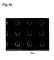
- Fig. 10 is a SEM photograph of the optical function part in the SERS element of Example 3.
- Au was vapor-deposited as a conductor layer with a thickness of 100 nm.
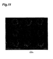
- FIG. 11 is a SEM photograph of the optical function part in the SERS element of Example 4.
- Au was vapor-deposited as a conductor layer with a thickness of 200 nm.
- Figs. 8 and 9 is a SEM photographs capturing the optical function part in a direction tilted by 30° from a direction perpendicular to the surface of the substrate.
- the SERS elements of Examples 1 to 4 were made as follows. First, using a mold in which holes, each having a hole diameter of 120 nm and a hole depth of 180 nm, were arranged in a square lattice at a hole interval (distance between center lines of holes adjacent to each other) of 360 nm, a resin on a substrate made of glass was molded by nanoimprinting, so as to produce a fine structure part.
- the pillars had a diameter of 120 nm, a height of 150 nm, and a pillar pitch (distance between center lines of pillars adjacent to each other) of 360 nm.
- a film of Ti was formed as a buffer layer by resistance heating vacuum vapor deposition on the produced fine structure part.
- the film forming condition for the buffer layer was "film thickness: 2 nm; vapor deposition rate: 0.02 nm/s; degree of vacuum during film forming: 2 ⁇ 10 -5 torr; substrate rotation: none; substrate temperature control: none.”
- a film of Au was formed as a conductor layer by resistance heating vacuum vapor deposition on the buffer layer, so as to yield the SERS elements of Examples 1 to 4.
- the film forming condition for the conductor layer was "film thickness: as mentioned above; vapor deposition rate: 0.02 nm/s; degree of vacuum during film forming: 1.5 ⁇ 10 -5 torr; substrate rotation: none; substrate temperature control: none.”
- the gap formed by the base part and protrusion is easier to form under the following conditions.
- resistance heating vacuum vapor deposition or electron beam vapor deposition is preferred to sputtering. It seems that resistance heating vacuum vapor deposition or electron beam vapor deposition employs a vapor deposition source having a relatively small heating part, so that vapor deposition materials fly to the substrate with such favorable directivity as to be less likely to reach side faces of pillars, whereby vapor-deposited materials piled on leading end parts of the pillars are likely to cast shadows on bottom parts of the pillars.
- vapor deposition materials seem to fly from a relatively large gold target surface toward the side faces of pillars as well, thereby making it harder for gaps to occur in the bottom parts of the pillars.
- the substrate it is preferable for the substrate to stand still during vapor deposition.
- better stability in film thickness is attained when revolving the wafers about the vapor deposition source while keeping a fixed angle thereto without rotating them.
- ring-slit-shaped gaps are generated in root parts of the protrusions of the conductor layer in Example 1 (with the Au film thickness of 30 nm).
- Example 2 the Au film thickness of 50 nm
- Example 3 the Au film thickness of 100 nm
- Example 4 the Au film thickness of 200 nm
- the protrusions in the conductor layer become laterally thicker, and the ring-slit-shaped gaps formed in the root parts of the protrusions are also made greater.
- the ring-slit-shaped gaps are generated either when the thickness of the conductor layer (i.e., the thickness of the base part of the conductor layer) is smaller (Examples 1 to 3) or greater (Example 4) than the height of the pillars.
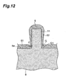
- the root part of the pillar 11 when the thickness of the base part 61 is smaller than the height of the pillar 11, the root part of the pillar 11 (i.e., the corner part defined by the surface 8a of the support part 8 and the side face of the pillar 11) may be free of the space S illustrated in Fig. 4 .
- the root part of the pillar 11 may be free of the space S illustrated in Fig. 5 when the thickness of the base part 61 is greater than the height of the pillar 11.
- Fig. 14 is a SEM photograph of the optical function part in the SERS element of Example 5.
- Fig. 14 is a SEM photograph of the optical function part in the SERS element of Example 5.
- Fig. 14 is a SEM photograph capturing the optical function part in a direction tilted by 30° from a direction perpendicular to the surface of the substrate.
- the SERS element of Example 5 was made as follows. First, as with the above-mentioned Examples 1 to 4, a resin on the substrate made of glass was molded by nanoimprinting, so as to make a fine structure part. In thus produced fine structure part, the pillars had a diameter of 120 nm, a height of 150 nm, and a pillar pitch (distance between center lines of pillers adjacent to each other) of 360 nm.
- a film of Ti was formed as a buffer layer by resistance heating vacuum vapor deposition on the produced fine structure part.
- the film forming condition for the buffer layer was "film thickness: 2 nm; vapor deposition rate: 0.02 nm/s; degree of vacuum during film forming: 2 ⁇ 10 -5 torr; substrate rotation: none; substrate temperature control: none.”
- a film of Au was formed as a conductor layer by sputtering on the buffer layer, so as to yield a continuous Au film as illustrated in (a) of Fig. 14 .
- the film forming condition for the conductor layer was "film thickness: 50 nm; film forming time: 5 min; atmosphere gas: air; substrate rotation: none; substrate temperature control: none.” Then, a film of Au was formed as a conductor layer by resistance heating vapor deposition method on the continuous Au film, so as to yield the SERS element of Example 5 as illustrated in (b) of Fig. 14 .
- the film forming condition for the continuous Au film was "film thickness: 50 nm; vapor deposition rate: 0.02 nm/s; degree of vacuum during film forming: 1.5 ⁇ 10 -5 torr; substrate rotation: none; substrate temperature control: none.”
- the continuous Au film formed by sputtering is a film which is continuous so as to cover the whole surface of the fine structure part.
- ring-slit-shaped gaps are generated in root parts of the protrusions of the conductor layer also when a film of Au is formed by resistance heating vacuum vapor deposition as a conductor layer on the continuous Au film.
- Fig. 15 is a graph illustrating relationships between Stokes shift and signal intensity concerning the surface-enhanced Raman scattering elements of Examples 2 and 5.
- the SERS elements of Examples 2 and 5 were dipped in an ethanol solution of mercaptobenzonic acid (1 mM) for two hours, then rinsed with ethanol, and dried with a nitrogen gas, so that a sample was arranged on the optical function part of the SERS element.
- the sample was subjected to Raman spectrometry with excitation light having a wavelength of 785 nm. This resulted in SERS spectra of mercaptobenzonic acid with substantially the same signal intensity in both Examples 2 and 5 as illustrated in Fig. 15 .
- the intensity of surface-enhanced Raman scattering is seen to increase regardless of whether or not there is the space S in root parts of the pillar 11 (i.e., the corner part defined by the surface 8a of the support part 8 and the side face of the pillar 11).
- Fig. 16 is a graph illustrating a relationship between Stokes shift and signal intensity concerning the surface-enhanced Raman scattering element of Example 2.
- an aqueous solution of 4,4'-bipyridyl (0.1 ⁇ M) was dropped onto the optical function part of the SERS element of Example 2, and a glass cover was put thereon as a lid so as to keep it from drying, whereby a sample was arranged on the optical function part.
- the sample was subjected to Raman spectrometry with excitation light having a wavelength of 785 nm. This resulted in a SERS spectrum of 4,4'-bipyridyl as illustrated in Fig. 16 .
- FIG. 17 (a) and (b) are graphs illustrating relationships between pillar pitch and signal intensity in the surface-enhanced Raman scattering elements of Examples 2 and 5, respectively. These graphs show results concerning a peak intensity at a Stokes shift of 1072 cm -1 in the case of Fig. 15 . It is seen from (a) and (b) of Fig. 17 that the intensity of surface-enhanced Raman scattering depends on the pillar pitch (distance between the center lines of pillars adjacent to each other) and that the pillar pitch is preferably 250 nm to 800 nm in order to increase the intensity of surface-enhanced Raman scattering. These plots are substantially applicable even when the diameter of pillars varies.
- duty in the graphs of (a) and (b) in Fig. 17 is meant the ratio between the pillar width and the space between pillars in the fine structure part.
- the present invention is not limited to the above-mentioned embodiment.
- the pillars 11 may be arranged one-dimensionally instead of two-dimensionally or in a triangular lattice instead of a square lattice.
- the cross-sectional form of the pillars 11 is not limited to circles, but may be ellipses or polygons such as triangles and quadrangles.
- various materials and forms can be employed for constituents of the SERS element 3 and SERS unit 1.
- the width of the gap formed by the based part and the protrusion is smaller than the distance between the conductor layer formed on the outer surface of one projection and that formed on the outer surface of the other projection. This can easily and stably form such a narrow gap (gap favorably functioning as a nanogap) as to be unattainable by the configuration of the fine structure part alone.
- the fine structure part 7 may be formed on the front face 4a of the substrate 4 either indirectly with the support part 8, for example, interposed therebetween as in the above-mentioned embodiment or directly.
- the conductor layer 6 may be formed on the fine structure part 7 either indirectly with a layer such as a buffer metal (Ti, Cr, or the like) for improving the adhesion of a metal to the fine structure part 7, for example, interposed therebetween or directly.
- the base part 61 and protrusion 62 may be separated from each other at the deepest part of the gap G.
- An end part on the substrate 4 side of the protrusion 62 located closer to the substrate than is the upper face of the base part 61 also forms a favorable nanogap with the base part 61 while curving radially of the pillar 11, which can increase the intensity of surface-enhanced Raman scattering in this case as well.
- the present invention can provide a surface-enhanced Raman scattering element which can increase the intensity of surface-enhanced Raman scattering by a favorable nanogap.
- SERS element surface-enhanced Raman scattering element
- 4 substrate
- 4a front face (principal surface)
- 6 conductor layer
- 7 fine structure part
- 10 optical function part
- 11 pillar (projection)
- 61 base part
- 62 protrusion
- G gap.
Landscapes
- Health & Medical Sciences (AREA)
- Physics & Mathematics (AREA)
- Life Sciences & Earth Sciences (AREA)
- Chemical & Material Sciences (AREA)
- Analytical Chemistry (AREA)
- Biochemistry (AREA)
- General Health & Medical Sciences (AREA)
- General Physics & Mathematics (AREA)
- Immunology (AREA)
- Pathology (AREA)
- Nuclear Medicine, Radiotherapy & Molecular Imaging (AREA)
- Investigating, Analyzing Materials By Fluorescence Or Luminescence (AREA)
Abstract
Description
- The present invention relates to a surface-enhanced Raman scattering element.
- As a conventional surface-enhanced Raman scattering element, one equipped with a minute metal structure configured to generate surface-enhanced Raman scattering (SERS) has been known (see, for example,
Patent Literature 1 and Non Patent Literature 1). In such a surface-enhanced Raman scattering element, when a sample to be subjected to Raman spectroscopic analysis is brought into contact with the minute metal structure and is irradiated with excitation light in this state, surface-enhanced Raman scattering occurs, whereby Raman scattering light enhanced by about 108 times, for example, is released. - Meanwhile, for example,
Patent Literature 2 discloses a minute metal structure in which metal layers are formed on one surface of a substrate and upper faces of a plurality of minute projections formed on the one surface of the substrate (or bottom faces of a plurality of fine holes formed on the one surface of the substrate) so as to be out of contact with each other (such that the shortest distance therebetween is on the order of 5 nm to 10 µm). -
- Patent Literature 1: Japanese Patent Application Laid-Open No.
2011-33518 - Patent Literature 2: Japanese Patent Application Laid-Open No.
2009-222507 - Non Patent Literature 1: "Q-SERS™ G1 Substrate", [online], Opto Science, Inc., [retrieved on 2012-07-19]. Retrieved from the Internet: < URL: http://www optoscience.com/maker/nanova/pdf/Q-SERS_G1.pdf>.
- When a minute metal structure is formed with a so-called nanogap as mentioned above, electric fields are locally enhanced upon irradiation with excitation light, whereby the intensity of surface-enhanced Raman scattering increases.
- It is therefore an object of the present invention to provide a surface-enhanced Raman scattering element which can increase the intensity of surface-enhanced Raman scattering by a favorable nanogap.
- The surface-enhanced Raman scattering element in accordance with one aspect of the present invention comprises a substrate having a principal surface; a fine structure part formed on the principal surface and having a plurality of projections; and a conductor layer formed on the fine structure part and constituting an optical function part for generating surface-enhanced Raman scattering; the conductor layer having a base part formed along the principal surface and a plurality of protrusions protruding from the base part at respective positions corresponding to the projections; the base part and protrusions forming a plurality of gaps in the conductor layer, each of the gaps having an interstice gradually decreasing in a direction perpendicular to the projecting direction of the projections.
- In this surface-enhanced Raman scattering element, the base part and protruding parts form a plurality of gaps, each of the gaps having an interstice gradually decreasing in a direction perpendicular to the projecting direction of the projections, in the conductor layer constituting the optical function part. The gaps formed in this conductor layer favorably function as nanogaps where electric fields are enhanced. Therefore, this surface-enhanced Raman scattering element can increase the intensity of surface-enhanced Raman scattering by favorable nanogaps.
- In the surface-enhanced Raman scattering element in accordance with one aspect of the present invention, the projections may be arranged periodically along the principal surface. This configuration can increase the intensity of surface-enhanced Raman scattering.
- In the surface-enhanced Raman scattering element in accordance with one aspect of the present invention, the gaps may be formed so as to surround the respective projections when seen in the projecting direction of the projections and each of the gaps may have the interstice gradually decreasing at an end part on the substrate side. This configuration can increase the gaps favorably functioning as nanogaps.
- In the surface-enhanced Raman scattering element in accordance with one aspect of the present invention, the interstice of the gap may gradually decrease continuously. This configuration enables the gaps formed by the base part and protrusions to function securely as nanogaps.
- In the surface-enhanced Raman scattering element in accordance with one aspect of the present invention, the protrusion may have a form constricted at an end part on the substrate side. This configuration can easily and securely yield the gap gradually decreasing the interstice in a direction perpendicular to the projecting direction of the projections.
- In the surface-enhanced Raman scattering element in accordance with one aspect of the present invention, the base part may have a thickness either smaller or greater than a height of the projections. Either configuration can increase the intensity of surface-enhanced Raman scattering by favorable nanogaps.
- In the surface-enhanced Raman scattering element in accordance with one aspect of the present invention, the base part and protrusion may be either connected to each other or separated from each other at the deepest part of the gap. Either configuration can increase the intensity of surface-enhanced Raman scattering by favorable nanogaps.
- The present invention can provide a surface-enhanced Raman scattering element which can increase the intensity of surface-enhanced Raman scattering by a favorable nanogap.
-
-
Fig. 1 is a plan view of a surface-enhanced Raman scattering unit equipped with a surface-enhanced Raman scattering element in accordance with an embodiment of the present invention; -
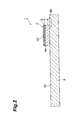
Fig. 2 is a sectional view taken along the line II-II ofFig. 1 ; -
Fig. 3 is a vertical sectional view of an optical function part in the surface-enhanced Raman scattering element ofFig. 1 ; -
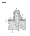
Fig. 4 is a vertical sectional view of a pillar and a conductor layer in the optical function part ofFig. 3 ; -
Fig. 5 is a vertical sectional view of the pillar and conductor layer in a modified example of the optical function part ofFig. 3 ; -
Fig. 6 is a sectional view illustrating steps of manufacturing the surface-enhanced Raman scattering element ofFig. 1 ; -
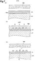
Fig. 7 is a sectional view illustrating steps of manufacturing the surface-enhanced Raman scattering element ofFig. 1 ; -
Fig. 8 is a SEM photograph of the optical function part in the surface-enhanced Raman scattering element of Example 1; -
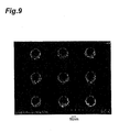
Fig. 9 is a SEM photograph of the optical function part in the surface-enhanced Raman scattering element of Example 2; -
Fig. 10 is a SEM photograph of the optical function part in the surface-enhanced Raman scattering element of Example 3; -
Fig. 11 is a SEM photograph of the optical function part in the surface-enhanced Raman scattering element of Example 4; -
Fig. 12 is a vertical sectional view of the pillar and conductor layer in a modified example of the optical function part ofFig. 3 ; -
Fig. 13 is a vertical sectional view of the pillar and conductor layer in a modified example of the optical function part ofFig. 3 ; -
Fig. 14 is a SEM photograph of the optical function part in the surface-enhanced Raman scattering element of Example 5; -
Fig. 15 is a graph illustrating relationships between Stokes shift and signal intensity concerning the surface-enhanced Raman scattering elements of Examples 2 and 5; -
Fig. 16 is a graph illustrating a relationship between Stokes shift and signal intensity concerning the surface-enhanced Raman scattering element of Example 2; -
Fig. 17 is a graph illustrating relationships between pillar pitch and signal intensity concerning the surface-enhanced Raman scattering elements of Examples 2 and 5; and -
Fig. 18 is a vertical sectional view of the pillar and conductor layer in a modified example of the optical function part ofFig. 3 . - In the following, preferred embodiments of the present invention will be explained in detail with reference to the drawings. In the drawings, the same or equivalent parts will be referred to with the same signs while omitting their overlapping descriptions.
- As illustrated in
Figs. 1 and2 , a SERS unit (surface-enhanced Raman scattering unit) 1 comprises ahandling board 2 and a SERS element (surface-enhanced Raman scattering element) 3 attached onto thehandling board 2. Thehandling board 2 is a rectangular plate-shaped glass slide, resin board, ceramic board, or the like. TheSERS element 3 is arranged on afront face 2a of thehandling board 2 while being biased to one end part in the longitudinal direction of thehandling board 2. - The
SERS element 3 comprises asubstrate 4 attached onto thehandling board 2, a moldedlayer 5 formed on thesubstrate 4, and aconductor layer 6 formed on the moldedlayer 5. Thesubstrate 4 is formed into a rectangular plate by silicon, glass, or the like and has an outer form on the order of several hundred µm × several hundred µm to several ten mm × several ten mm and a thickness on the order of 100 µm to 2 mm. Arear face 4b of thesubstrate 4 is secured to thefront face 2a of thehandling board 2 by direct bonding, bonding with a metal such as solder, eutectic bonding, fusion bonding by irradiation with laser light and the like, anodic bonding, or bonding with a resin. - As illustrated in
Fig. 3 , themolded layer 5 includes afine structure part 7, asupport part 8, and aframe part 9. Thefine structure part 7, which is a region having a periodic pattern, is formed on a surface layer on the side opposite from thesubstrate 4 at a center part of the moldedlayer 5. In thefine structure part 7, a plurality of circular columnar pillars (projections) 11, each having a diameter and height on the order of several nm to several hundred nm, are periodically arranged at a pitch on the order of several ten nm to several hundred nm (preferably 250 nm to 800 nm) along a front face (principal surface) 4a of thesubstrate 4. Thefine structure part 7 has a rectangular outer form on the order of several mm × several mm when seen in the thickness direction of thesubstrate 4. Thesupport part 8, which is a rectangular region supporting thefine structure part 7, is formed on thefront face 4a of thesubstrate 4. Theframe part 9, which is a rectangular ring-shaped region surrounding thesupport part 8, is formed on thefront face 4a of thesubstrate 4. Thesupport part 8 and framepart 9 have a thickness on the order of several ten nm to several ten µm. The moldedlayer 5 like this is integrally formed by molding a resin (examples of which include resins based on acrylics, fluorine, epoxy, silicone, and urethane, PET, polycarbonate, and inorganic/organic hybrid materials) or low-melting glass arranged on thesubstrate 4 by nanoimprinting, for example. - The
conductor layer 6 is formed over thefine structure part 7 and framepart 9. In thefine structure part 7, theconductor layer 6 reaches asurface 8a of thesupport part 8 which is exposed to the side opposite from thesubstrate 4. Theconductor layer 6 has a thickness on the order of several nm to several µm. Theconductor layer 6 like this is formed by vapor-depositing a conductor such as a metal (Au, Ag, Al, Cu, Pt, or the like) on the moldedlayer 5 molded by nanoimprinting, for example. In theSERS element 3, theconductor layer 6 formed on thefine structure part 7 and thesurface 8a of thesupport part 8 constructs anoptical function part 10 which generates surface-enhanced Raman scattering. - As illustrated in
Fig. 4 , theconductor layer 6 has abase part 61 formed along thefront face 4a of thesubstrate 4 and a plurality ofprotrusions 62 protruding from thebase part 61 at respective positions corresponding to thepillars 11. Thebase part 61 is formed like a layer on thesurface 8a of thesupport part 8. Thebase part 61 has a thickness on the order of several nm to several hundred nm, which is smaller than the height of thepillars 11. Eachprotrusion 62 is formed so as to cover itscorresponding pillar 11 and has a form constricted at least at an end part on thesubstrate 4 side. The end part on thesubstrate 4 side of theprotrusion 62 is located closer to the substrate than is the upper face of thebase part 61. - In the
conductor layer 6, thebase part 61 andprotrusions 62 form a plurality of gaps G in which an interstice d in a direction perpendicular to the projecting direction of thepillars 11 gradually decreases. The gap G has the interstice d on the order of 0 to several ten nm. The gap G is formed into a circular ring so as to surround itscorresponding pillar 11 when seen in the projecting direction of thepillar 11, while the interstice d gradually decreases continuously at an end part G1 on thesubstrate 4 side. That is, the interstice d of the gap G in a direction perpendicular to the projecting direction of thepillar 11 gradually becomes smaller toward thesubstrate 4. Here, thebase part 61 andprotrusion 62 are connected to each other at the deepest part of the gap G, while a space S is formed at a root part of the pillar 11 (i.e., a corner part defined by thesurface 8a of thesupport part 8 and the side face of the pillar 11). This space S is formed depending on a vapor deposition condition for forming theconductor layer 6 on thefine structure part 7 by vapor deposition and the like. - As illustrated in
Fig. 5 , the thickness of thebase part 61 may be greater than the height of thepillar 11, and theprotrusion 62 may be formed on an extension of itscorresponding pillar 11. In theconductor layer 6, thebase part 61 andprotrusion 62 form the gap G gradually decreasing the interstice d in a direction perpendicular to the projecting direction of thepillar 11 in this case as well. - The
SERS unit 1 constructed as in the foregoing is used as follows. First, a ring-shaped spacer made of silicone, for example, is arranged on thefront face 2a of the handlingboard 2 so as to surround theSERS element 3. Subsequently, a sample of a solution (or a dispersion of a powder sample in a solution such as water or ethanol) is dropped to the inside of the spacer with a pipette or the like, so as to arrange the sample on theoptical function part 10. Then, for preventing the solvent from evaporating and for reducing the lens effect, a glass cover is mounted on the spacer and brought into close contact with the solution sample. - Next, the
SERS unit 1 is set in a Raman spectroscopic analyzer, and the sample arranged on theoptical function part 10 is irradiated with excitation light through the glass cover. This generates surface-enhanced Raman scattering at the interface between theoptical function part 10 and sample, whereby surface-enhanced Raman scattering light derived from the sample is enhanced and released. Hence, the Raman spectroscopic analyzer enables Raman spectroscopy with high accuracy. - Not only the above-mentioned method, but the following methods may also be used for arranging the sample on the
optical function part 10. For example, while holding the handlingboard 2, theSERS element 3 may be dipped in and lifted from the solution sample (or a dispersion of a powder sample in a solution such as water or ethanol), and then the sample may be blown to dry. A minute amount of the solution sample (or a dispersion of a powder sample in a solution such as water or ethanol) may be dropped onto theoptical function part 10 and left to dry A powder sample may be dispersed as it is on theoptical function part 10. - An example of methods for manufacturing the
SERS element 3 will now be explained. First, as illustrated in (a) ofFig. 6 , a master mold MM and a film base F are prepared. The master mold MM includes a fine structure part M7 corresponding to thefine structure part 7 and a support part M8 for supporting the fine structure part M7. A plurality of fine structure parts M7 are arranged in a matrix on the support part M8. Subsequently, as illustrated in (b) ofFig. 6 , the film base F is pressed against the master mold MM and pressurized and heated in this state, so as to transfer a pattern of the plurality of fine structure parts M7 to the film base F. Then, as illustrated in (c) ofFig. 6 , the film base F is released from the master mold MM, so as to yield a replica mold (replica film) RM having the pattern of the plurality of fine structure parts M7 transferred thereto. The replica mold RM may also be one formed by applying a resin (examples of which include resins based on epoxy, acrylics, fluorine, silicone, and urethane and inorganic/organic hybrid resins) onto the film base F. When the resin to be applied onto the film base F is UV-curable, the replica mold R can be obtained by curing the resin applied on the film base F by irradiation with UV (UV nanoimprinting) instead of thermal nanoimprinting. - Next, as illustrated in (a) of
Fig. 7 , asilicone wafer 40 to become thesubstrate 4 is prepared, and a UV-curable resin is applied onto afront face 40a of thesilicon wafer 40, so as to form ananoimprinting layer 50 to become the moldedlayer 5 on thesilicone wafer 40. Subsequently, as illustrated in (b) ofFig. 7 , the replica mold RM is pressed against thenanoimprinting layer 50, and thenanoimprinting layer 50 is irradiated with UV in this state, so as to be cured, whereby the pattern of the replica mold RM is transferred to thenanoimprinting layer 50. Then, as illustrated in (c) ofFig. 7 , the replica mold RM is released from thenanoimprinting layer 50, so as to yield thesilicone wafer 40 formed with a plurality offine structure parts 7. - Next, a film of a metal such as Au or Ag is produced on the molded
layer 5 by vapor deposition, so as to form theconductor layer 6. Subsequently, thesilicone wafer 40 is cut for each fine structure part 7 (i.e., for each optical function part 10), whereby a plurality ofSERS elements 3 are obtained. For yielding theSERS unit 1, it is sufficient for theSERS element 3 manufactured as mentioned above to be attached onto the handlingboard 2. - The
fine structure part 7 may be formed on thesubstrate 4 by etching using a mask having a two-dimensional pattern formed by photoetching, electron beam lithography, or the like instead of the above-mentioned nanoimprinting. In either case, forming theconductor layer 6 on thefine structure part 7 by vapor deposition can produce theconductor layer 6 with the nano-order gaps G with a favorable reproducibility in a simple process, thereby enabling mass production of theSERS element 3. - In the
conductor layer 6 constituting theoptical function part 10 in theSERS element 3, a plurality of gaps G in which the interstice d in a direction perpendicular to the projecting direction of thepillar 11 gradually decreases are formed by thebase part 61 andprotrusions 62 as explained in the foregoing. The gaps G formed in theconductor layer 6 favorably function as nanogaps (in particular in a part where the interstice d of the gaps G is 20 nm or less) where electric fields are locally enhanced. Therefore, theSERS element 3 can increase the intensity of surface-enhanced Raman scattering by favorable nanogaps. - Since a plurality of
pillars 11 are arranged periodically along thefront face 4a of thesubstrate 4, the intensity of surface-enhanced Raman scattering can be increased. - The gap G is formed so as to surround the
pillar 11 when seen in the projecting direction of thepillar 11, while the interstice d gradually decreases at the end part on thesubstrate 4 side, whereby the gaps G favorably functioning as nanogaps can be increased. - Since the interstice of the gap G gradually decreases continuously, the gap G can securely function as a nanogap.
- Since the
protrusion 62 has a form constricted at the end part on thesubstrate 4 side, the gap G gradually decreasing the interstice d in a direction perpendicular to the projecting direction of thepillar 11 can be obtained easily and securely. - Examples of the
SERS element 3 having thepillar 11 andconductor layer 6 illustrated inFigs. 4 and5 will now be explained.Fig. 8 is a SEM photograph of the optical function part in the SERS element of Example 1. In Example 1, Au was vapor-deposited as a conductor layer with a thickness of 30 nm.Fig. 9 is a SEM photograph of the optical function part in the SERS element of Example 2. In Example 2, Au was vapor-deposited as a conductor layer with a thickness of 50 nm.Fig. 10 is a SEM photograph of the optical function part in the SERS element of Example 3. In Example 3, Au was vapor-deposited as a conductor layer with a thickness of 100 nm.Fig. 11 is a SEM photograph of the optical function part in the SERS element of Example 4. In Example 4, Au was vapor-deposited as a conductor layer with a thickness of 200 nm. Each ofFigs. 8 and9 is a SEM photographs capturing the optical function part in a direction tilted by 30° from a direction perpendicular to the surface of the substrate. - The SERS elements of Examples 1 to 4 were made as follows. First, using a mold in which holes, each having a hole diameter of 120 nm and a hole depth of 180 nm, were arranged in a square lattice at a hole interval (distance between center lines of holes adjacent to each other) of 360 nm, a resin on a substrate made of glass was molded by nanoimprinting, so as to produce a fine structure part. In thus produced fine structure part, the pillars had a diameter of 120 nm, a height of 150 nm, and a pillar pitch (distance between center lines of pillars adjacent to each other) of 360 nm.
- Next, a film of Ti was formed as a buffer layer by resistance heating vacuum vapor deposition on the produced fine structure part. The film forming condition for the buffer layer was "film thickness: 2 nm; vapor deposition rate: 0.02 nm/s; degree of vacuum during film forming: 2 × 10⁻⁵ torr; substrate rotation: none; substrate temperature control: none." Subsequently, a film of Au was formed as a conductor layer by resistance heating vacuum vapor deposition on the buffer layer, so as to yield the SERS elements of Examples 1 to 4. The film forming condition for the conductor layer was "film thickness: as mentioned above; vapor deposition rate: 0.02 nm/s; degree of vacuum during film forming: 1.5 × 10⁻⁵ torr; substrate rotation: none; substrate temperature control: none."
- The gap formed by the base part and protrusion (gap gradually decreasing the interstice in a direction perpendicular to the projecting direction of the protrusion) is easier to form under the following conditions. First, resistance heating vacuum vapor deposition or electron beam vapor deposition is preferred to sputtering. It seems that resistance heating vacuum vapor deposition or electron beam vapor deposition employs a vapor deposition source having a relatively small heating part, so that vapor deposition materials fly to the substrate with such favorable directivity as to be less likely to reach side faces of pillars, whereby vapor-deposited materials piled on leading end parts of the pillars are likely to cast shadows on bottom parts of the pillars. In sputtering, on the other hand, vapor deposition materials seem to fly from a relatively large gold target surface toward the side faces of pillars as well, thereby making it harder for gaps to occur in the bottom parts of the pillars. Second, it is preferable for the substrate to stand still during vapor deposition. For mass production (for processing a plurality of wafers in a vapor deposition system), however, better stability in film thickness is attained when revolving the wafers about the vapor deposition source while keeping a fixed angle thereto without rotating them.
- As illustrated in
Fig. 8 , ring-slit-shaped gaps are generated in root parts of the protrusions of the conductor layer in Example 1 (with the Au film thickness of 30 nm). As illustrated inFigs. 9 to 11 , as the Au film thickness increases successively in Example 2 (the Au film thickness of 50 nm), Example 3 (the Au film thickness of 100 nm), and Example 4 (the Au film thickness of 200 nm), the protrusions in the conductor layer become laterally thicker, and the ring-slit-shaped gaps formed in the root parts of the protrusions are also made greater. Thus, the ring-slit-shaped gaps are generated either when the thickness of the conductor layer (i.e., the thickness of the base part of the conductor layer) is smaller (Examples 1 to 3) or greater (Example 4) than the height of the pillars. - Modified examples of the
optical function part 10 ofFig. 3 will now be explained. As illustrated inFig. 12 , when the thickness of thebase part 61 is smaller than the height of thepillar 11, the root part of the pillar 11 (i.e., the corner part defined by thesurface 8a of thesupport part 8 and the side face of the pillar 11) may be free of the space S illustrated inFig. 4 . Similarly, as illustrated inFig. 13 , the root part of thepillar 11 may be free of the space S illustrated inFig. 5 when the thickness of thebase part 61 is greater than the height of thepillar 11. - Examples of the
SERS element 3 having thepillar 11 andconductor layer 6 illustrated inFigs. 12 and13 will now be explained.Fig. 14 is a SEM photograph of the optical function part in the SERS element of Example 5.Fig. 14 is a SEM photograph of the optical function part in the SERS element of Example 5.Fig. 14 is a SEM photograph capturing the optical function part in a direction tilted by 30° from a direction perpendicular to the surface of the substrate. - The SERS element of Example 5 was made as follows. First, as with the above-mentioned Examples 1 to 4, a resin on the substrate made of glass was molded by nanoimprinting, so as to make a fine structure part. In thus produced fine structure part, the pillars had a diameter of 120 nm, a height of 150 nm, and a pillar pitch (distance between center lines of pillers adjacent to each other) of 360 nm.
- Next, a film of Ti was formed as a buffer layer by resistance heating vacuum vapor deposition on the produced fine structure part. The film forming condition for the buffer layer was "film thickness: 2 nm; vapor deposition rate: 0.02 nm/s; degree of vacuum during film forming: 2 × 10⁻⁵ torr; substrate rotation: none; substrate temperature control: none." Subsequently, a film of Au was formed as a conductor layer by sputtering on the buffer layer, so as to yield a continuous Au film as illustrated in (a) of
Fig. 14 . The film forming condition for the conductor layer was "film thickness: 50 nm; film forming time: 5 min; atmosphere gas: air; substrate rotation: none; substrate temperature control: none." Then, a film of Au was formed as a conductor layer by resistance heating vapor deposition method on the continuous Au film, so as to yield the SERS element of Example 5 as illustrated in (b) ofFig. 14 . The film forming condition for the continuous Au film was "film thickness: 50 nm; vapor deposition rate: 0.02 nm/s; degree of vacuum during film forming: 1.5 × 10⁻⁵ torr; substrate rotation: none; substrate temperature control: none." - As illustrated in (a) of
Fig. 14 , the continuous Au film formed by sputtering is a film which is continuous so as to cover the whole surface of the fine structure part. As illustrated in (b) ofFig. 14 , ring-slit-shaped gaps are generated in root parts of the protrusions of the conductor layer also when a film of Au is formed by resistance heating vacuum vapor deposition as a conductor layer on the continuous Au film. -
Fig. 15 is a graph illustrating relationships between Stokes shift and signal intensity concerning the surface-enhanced Raman scattering elements of Examples 2 and 5. Here, the SERS elements of Examples 2 and 5 were dipped in an ethanol solution of mercaptobenzonic acid (1 mM) for two hours, then rinsed with ethanol, and dried with a nitrogen gas, so that a sample was arranged on the optical function part of the SERS element. The sample was subjected to Raman spectrometry with excitation light having a wavelength of 785 nm. This resulted in SERS spectra of mercaptobenzonic acid with substantially the same signal intensity in both Examples 2 and 5 as illustrated inFig. 15 . The intensity of surface-enhanced Raman scattering is seen to increase regardless of whether or not there is the space S in root parts of the pillar 11 (i.e., the corner part defined by thesurface 8a of thesupport part 8 and the side face of the pillar 11). -
Fig. 16 is a graph illustrating a relationship between Stokes shift and signal intensity concerning the surface-enhanced Raman scattering element of Example 2. Here, an aqueous solution of 4,4'-bipyridyl (0.1 µM) was dropped onto the optical function part of the SERS element of Example 2, and a glass cover was put thereon as a lid so as to keep it from drying, whereby a sample was arranged on the optical function part. The sample was subjected to Raman spectrometry with excitation light having a wavelength of 785 nm. This resulted in a SERS spectrum of 4,4'-bipyridyl as illustrated inFig. 16 . - In
Fig. 17 , (a) and (b) are graphs illustrating relationships between pillar pitch and signal intensity in the surface-enhanced Raman scattering elements of Examples 2 and 5, respectively. These graphs show results concerning a peak intensity at a Stokes shift of 1072 cm-1 in the case ofFig. 15 . It is seen from (a) and (b) ofFig. 17 that the intensity of surface-enhanced Raman scattering depends on the pillar pitch (distance between the center lines of pillars adjacent to each other) and that the pillar pitch is preferably 250 nm to 800 nm in order to increase the intensity of surface-enhanced Raman scattering. These plots are substantially applicable even when the diameter of pillars varies. By "duty" in the graphs of (a) and (b) inFig. 17 is meant the ratio between the pillar width and the space between pillars in the fine structure part. - While an embodiment of the present invention is explained in the foregoing, the present invention is not limited to the above-mentioned embodiment. For example, the
pillars 11 may be arranged one-dimensionally instead of two-dimensionally or in a triangular lattice instead of a square lattice. The cross-sectional form of thepillars 11 is not limited to circles, but may be ellipses or polygons such as triangles and quadrangles. Thus, without being restricted to those mentioned above, various materials and forms can be employed for constituents of theSERS element 3 andSERS unit 1. - When attention is focused on a pair of projections (those corresponding to the pillars 11) adjacent to each other, the width of the gap formed by the based part and the protrusion is smaller than the distance between the conductor layer formed on the outer surface of one projection and that formed on the outer surface of the other projection. This can easily and stably form such a narrow gap (gap favorably functioning as a nanogap) as to be unattainable by the configuration of the fine structure part alone.
- The
fine structure part 7 may be formed on thefront face 4a of thesubstrate 4 either indirectly with thesupport part 8, for example, interposed therebetween as in the above-mentioned embodiment or directly. Theconductor layer 6 may be formed on thefine structure part 7 either indirectly with a layer such as a buffer metal (Ti, Cr, or the like) for improving the adhesion of a metal to thefine structure part 7, for example, interposed therebetween or directly. - As illustrated in
Fig. 18 , thebase part 61 andprotrusion 62 may be separated from each other at the deepest part of the gap G. An end part on thesubstrate 4 side of theprotrusion 62 located closer to the substrate than is the upper face of thebase part 61 also forms a favorable nanogap with thebase part 61 while curving radially of thepillar 11, which can increase the intensity of surface-enhanced Raman scattering in this case as well. - The present invention can provide a surface-enhanced Raman scattering element which can increase the intensity of surface-enhanced Raman scattering by a favorable nanogap.
- 3: SERS element (surface-enhanced Raman scattering element); 4: substrate; 4a: front face (principal surface); 6: conductor layer; 7: fine structure part; 10: optical function part; 11: pillar (projection); 61: base part; 62: protrusion; G: gap.
Claims (9)
- A surface-enhanced Raman scattering element comprising:a substrate having a principal surface;a fine structure part formed on the principal surface and having a plurality of projections; anda conductor layer formed on the fine structure part and constituting an optical function part for generating surface-enhanced Raman scattering;wherein the conductor layer has a base part formed along the principal surface and a plurality of protrusions protruding from the base part at respective positions corresponding to the projections; andwherein the base part and the protrusions form a plurality of gaps in the conductor layer, each of the gaps having an interstice gradually decreasing in a direction perpendicular to the projecting direction of the projection.
- A surface-enhanced Raman scattering element according to claim 1, wherein the projections are arranged periodically along the principal surface.
- A surface-enhanced Raman scattering element according to claim 1 or 2, wherein the gaps are formed so as to surround the respective projections when seen in the projecting direction of the projections and each of the gaps have the interstice gradually decreasing at an end part on the substrate side.
- A surface-enhanced Raman scattering element according to one of claims 1 to 3, wherein the interstice of the gap gradually decreases continuously.
- A surface-enhanced Raman scattering element according to one of claims 1 to 4, wherein the protrusion has a form constricted at an end part on the substrate side.
- A surface-enhanced Raman scattering element according to one of claims 1 to 5, wherein the base part has a thickness smaller than a height of the projections.
- A surface-enhanced Raman scattering element according to one of claims 1 to 5, wherein the base part has a thickness greater than a height of the projections.
- A surface-enhanced Raman scattering element according to one of claims 1 to 7, wherein the base part and the protrusion are connected to each other at the deepest part of the gap.
- A surface-enhanced Raman scattering element according to one of claims 1 to 7, wherein the base part and the protrusion are separated from each other at the deepest part of the gap.
Applications Claiming Priority (2)
| Application Number | Priority Date | Filing Date | Title |
|---|---|---|---|
| JP2012178765A JP6023509B2 (en) | 2012-08-10 | 2012-08-10 | Surface-enhanced Raman scattering unit |
| PCT/JP2013/071698 WO2014025029A1 (en) | 2012-08-10 | 2013-08-09 | Surface-enhanced raman scattering element |
Publications (3)
| Publication Number | Publication Date |
|---|---|
| EP2889607A1 true EP2889607A1 (en) | 2015-07-01 |
| EP2889607A4 EP2889607A4 (en) | 2016-09-28 |
| EP2889607B1 EP2889607B1 (en) | 2020-09-23 |
Family
ID=50068245
Family Applications (1)
| Application Number | Title | Priority Date | Filing Date |
|---|---|---|---|
| EP13828677.8A Active EP2889607B1 (en) | 2012-08-10 | 2013-08-09 | Surface-enhanced raman scattering element |
Country Status (6)
| Country | Link |
|---|---|
| US (1) | US9874523B2 (en) |
| EP (1) | EP2889607B1 (en) |
| JP (1) | JP6023509B2 (en) |
| CN (1) | CN104508468B (en) |
| TW (1) | TWI627127B (en) |
| WO (1) | WO2014025029A1 (en) |
Cited By (1)
| Publication number | Priority date | Publication date | Assignee | Title |
|---|---|---|---|---|
| DE112017001837T5 (en) | 2016-04-04 | 2018-12-20 | Valeo Embrayages | Arrangement for a device for transmitting torque, device for transmitting torque and their assembly method |
Families Citing this family (13)
| Publication number | Priority date | Publication date | Assignee | Title |
|---|---|---|---|---|
| JP5908370B2 (en) * | 2012-08-10 | 2016-04-26 | 浜松ホトニクス株式会社 | Surface-enhanced Raman scattering unit |
| CN104520696B (en) | 2012-08-10 | 2018-01-12 | 浜松光子学株式会社 | Surface-enhanced Raman scattering element and its manufacturing method |
| CN104508466B (en) | 2012-08-10 | 2018-07-17 | 浜松光子学株式会社 | Surface enhanced raman scattering element |
| JP6294797B2 (en) * | 2014-09-10 | 2018-03-14 | 浜松ホトニクス株式会社 | Surface-enhanced Raman scattering unit |
| CN107075661B (en) * | 2014-09-26 | 2020-03-17 | 韩国机械研究院 | Substrate formed with a plurality of nanogaps and method for preparing the same |
| KR101639684B1 (en) * | 2014-09-29 | 2016-07-15 | 한국기계연구원 | adjusted nano-gap substrate and fabricating method for the same |
| KR101639686B1 (en) * | 2014-09-29 | 2016-07-25 | 한국기계연구원 | substrate which have multiple nano-gaps and fabricating method for the same |
| CN107561053B (en) * | 2016-07-01 | 2020-04-28 | 清华大学 | Single molecule detection method |
| JP6559187B2 (en) * | 2016-07-01 | 2019-08-14 | ツィンファ ユニバーシティ | Carrier for single molecule detection and single molecule detector |
| CN106292200B (en) * | 2016-09-19 | 2018-05-29 | 苏州大学 | Method for holographically manufacturing surface Raman enhanced substrate and photoetching system |
| KR102046436B1 (en) * | 2018-04-26 | 2019-11-19 | 한국기계연구원 | Substrate with sliding dielectric film and fabricating method for the same |
| TWI856328B (en) * | 2022-06-10 | 2024-09-21 | 國立臺北科技大學 | A substrate having a top angle thin film grating structure |
| KR20240034365A (en) * | 2022-09-07 | 2024-03-14 | 한국재료연구원 | 3D nano- plasmonic cavity substrate and the manufacturing method thereof |
Family Cites Families (56)
| Publication number | Priority date | Publication date | Assignee | Title |
|---|---|---|---|---|
| JPH0544867U (en) | 1991-11-18 | 1993-06-15 | 三洋電機株式会社 | Measuring device package |
| JPH07260646A (en) | 1994-03-17 | 1995-10-13 | Nikon Corp | Sample container |
| US20040023046A1 (en) | 1998-08-04 | 2004-02-05 | Falko Schlottig | Carrier substrate for Raman spectrometric analysis |
| JP2003026232A (en) | 2001-07-18 | 2003-01-29 | Seiko Epson Corp | Packing method and cushioning material |
| US7460224B2 (en) | 2005-12-19 | 2008-12-02 | Opto Trace Technologies, Inc. | Arrays of nano structures for surface-enhanced Raman scattering |
| CN100357738C (en) | 2004-03-26 | 2007-12-26 | 博奥生物有限公司 | Method of detecting small molecule compound and its special biochip |
| RU2361193C2 (en) | 2004-05-19 | 2009-07-10 | Вп Холдинг, Ллс | Optical sensor with multilayered plasmon structure for improved detection of chemical groups through sers |
| JP2005337771A (en) | 2004-05-25 | 2005-12-08 | National Institute For Materials Science | Integrated pillar structure optical element having nanostructure |
| GB0424458D0 (en) * | 2004-11-04 | 2004-12-08 | Mesophotonics Ltd | Metal nano-void photonic crystal for enhanced raman spectroscopy |
| US7245370B2 (en) | 2005-01-06 | 2007-07-17 | Hewlett-Packard Development Company, L.P. | Nanowires for surface-enhanced Raman scattering molecular sensors |
| US7528948B2 (en) | 2006-07-25 | 2009-05-05 | Hewlett-Packard Development Company, L.P. | Controllable surface enhanced Raman spectroscopy |
| EP2074421B1 (en) | 2006-10-12 | 2014-12-17 | Koninklijke Philips N.V. | Fast biosensor with reagent layer |
| US7388661B2 (en) * | 2006-10-20 | 2008-06-17 | Hewlett-Packard Development Company, L.P. | Nanoscale structures, systems, and methods for use in nano-enhanced raman spectroscopy (NERS) |
| JP2008196992A (en) | 2007-02-14 | 2008-08-28 | National Institute Of Information & Communication Technology | Electric field enhancement structure of surface plasmons |
| JP5397577B2 (en) | 2007-03-05 | 2014-01-22 | オムロン株式会社 | Surface plasmon resonance sensor and chip for the sensor |
| JP2008268059A (en) | 2007-04-23 | 2008-11-06 | St Japan Inc | Sample holder |
| JP4993360B2 (en) | 2007-06-08 | 2012-08-08 | 富士フイルム株式会社 | MICROSTRUCTURE, MANUFACTURING METHOD THEREOF, PHOTOELECTRIC FIELD ENHANCER DEVICE |
| JP2009047623A (en) | 2007-08-22 | 2009-03-05 | Jiyasuko Eng Kk | Transmission measuring holder |
| JP2009103643A (en) | 2007-10-25 | 2009-05-14 | Fujifilm Corp | Surface enhanced Raman spectrometer |
| US8115920B2 (en) | 2007-11-14 | 2012-02-14 | 3M Innovative Properties Company | Method of making microarrays |
| JP2009222507A (en) | 2008-03-14 | 2009-10-01 | National Institute Of Advanced Industrial & Technology | Trace material detection element |
| JP2009236830A (en) * | 2008-03-28 | 2009-10-15 | Sumitomo Precision Prod Co Ltd | Analyte carrier and its manufacturing method |
| CN101281133B (en) | 2008-05-12 | 2010-08-18 | 中国科学院合肥物质科学研究院 | Preparation of surface reinforced Raman active substrate of large area micro-nano dendritical structure array |
| US8198706B2 (en) | 2008-07-25 | 2012-06-12 | Hewlett-Packard Development Company, L.P. | Multi-level nanowire structure and method of making the same |
| JP4980324B2 (en) | 2008-09-30 | 2012-07-18 | テルモ株式会社 | Component measuring device |
| JP5042371B2 (en) | 2008-10-30 | 2012-10-03 | 日本電信電話株式会社 | Measuring chip attaching / detaching device, SPR measuring system, and measuring chip attaching / detaching method |
| CN102282094A (en) | 2008-11-17 | 2011-12-14 | 惠普开发有限公司 | A substrate for surface enhanced raman scattering (SERS) |
| JP5632751B2 (en) | 2009-02-09 | 2014-11-26 | 浜松ホトニクス株式会社 | Processing object cutting method |
| EP2419733A4 (en) | 2009-04-13 | 2013-12-25 | Univ Leland Stanford Junior | METHODS AND DEVICES FOR DETECTING THE PRESENCE OF AN ANALYTE IN A SAMPLE |
| US20120081703A1 (en) | 2009-05-07 | 2012-04-05 | Nant Holdings Ip, Llc | Highly Efficient Plamonic Devices, Molecule Detection Systems, and Methods of Making the Same |
| JP2011021085A (en) | 2009-07-15 | 2011-02-03 | Yokohama Rubber Co Ltd:The | Rubber composition for pneumatic tire |
| JP2011033518A (en) | 2009-08-04 | 2011-02-17 | Toray Res Center:Kk | Surface intensifying raman spectroscopy |
| US8659391B2 (en) | 2009-08-18 | 2014-02-25 | Indian Institute Of Technology Madras | Multielement and multiproperty tagging |
| EP2478343A1 (en) | 2009-09-17 | 2012-07-25 | Hewlett-Packard Development Company, L.P. | Electrically driven devices for surface enhanced raman spectroscopy |
| TWI523950B (en) | 2009-09-30 | 2016-03-01 | 凸版印刷股份有限公司 | Nucleic acid analysis apparatus |
| JP2011075348A (en) | 2009-09-30 | 2011-04-14 | Nidek Co Ltd | Method for manufacturing test piece |
| WO2011047690A1 (en) * | 2009-10-23 | 2011-04-28 | Danmarks Tekniske Universitet | Surface enhanced raman scattering substrates consumables for raman spectroscopy |
| JP5544836B2 (en) * | 2009-11-19 | 2014-07-09 | オムロン株式会社 | Surface plasmon resonance chip |
| US20110166045A1 (en) * | 2009-12-01 | 2011-07-07 | Anuj Dhawan | Wafer scale plasmonics-active metallic nanostructures and methods of fabricating same |
| JP5589656B2 (en) | 2009-12-11 | 2014-09-17 | セイコーエプソン株式会社 | Sensor chip, sensor cartridge and analyzer |
| JP5574783B2 (en) | 2010-03-31 | 2014-08-20 | 富士フイルム株式会社 | Fluorescence detection apparatus and method |
| US8358407B2 (en) | 2010-04-30 | 2013-01-22 | Hewlett-Packard Development Company, L.P. | Enhancing signals in Surface Enhanced Raman Spectroscopy (SERS) |
| US20140154668A1 (en) * | 2010-05-21 | 2014-06-05 | The Trustees Of Princeton University | Structures for Enhancement of Local Electric Field, Light Absorption, Light Radiation, Material Detection and Methods for Making and Using of the Same. |
| US9182338B2 (en) | 2010-05-21 | 2015-11-10 | The Trustees Of Princeton University | Structures for enhancement of local electric field, light absorption, light radiation, material detection and methods for making and using of the same |
| JP2012050073A (en) | 2010-07-30 | 2012-03-08 | Nikon Corp | Imaging device and image synthesis program |
| JP5779963B2 (en) | 2011-04-28 | 2015-09-16 | ナノフォトン株式会社 | Observation sample sealed container |
| WO2013015810A2 (en) | 2011-07-27 | 2013-01-31 | Hewlett-Packard Development Company, L.P. | Surface enhanced raman spectroscopy employing a nanorod in a surface indentation |
| TWI469917B (en) * | 2012-08-09 | 2015-01-21 | Nat Univ Tsing Hua | A sers-active structure, a fabrication method thereof, and a detection device comprising the same |
| EP4033222A1 (en) | 2012-08-10 | 2022-07-27 | Hamamatsu Photonics K.K. | Surface-enhanced raman scattering unit |
| CN108827928B (en) | 2012-08-10 | 2021-12-24 | 浜松光子学株式会社 | Surface enhanced Raman scattering unit and using method thereof |
| JP5945192B2 (en) * | 2012-08-10 | 2016-07-05 | 浜松ホトニクス株式会社 | Surface-enhanced Raman scattering unit |
| CN104508466B (en) * | 2012-08-10 | 2018-07-17 | 浜松光子学株式会社 | Surface enhanced raman scattering element |
| CN104520696B (en) * | 2012-08-10 | 2018-01-12 | 浜松光子学株式会社 | Surface-enhanced Raman scattering element and its manufacturing method |
| JP6055234B2 (en) * | 2012-08-10 | 2016-12-27 | 浜松ホトニクス株式会社 | Surface-enhanced Raman scattering unit |
| JP5908370B2 (en) | 2012-08-10 | 2016-04-26 | 浜松ホトニクス株式会社 | Surface-enhanced Raman scattering unit |
| CN104541158B (en) * | 2012-08-10 | 2017-05-24 | 浜松光子学株式会社 | Surface-enhanced Raman scattering element, and method of manufacturing surface-enhanced Raman scattering element |
-
2012
- 2012-08-10 JP JP2012178765A patent/JP6023509B2/en active Active
-
2013
- 2013-08-09 WO PCT/JP2013/071698 patent/WO2014025029A1/en not_active Ceased
- 2013-08-09 TW TW102128771A patent/TWI627127B/en not_active IP Right Cessation
- 2013-08-09 US US14/420,422 patent/US9874523B2/en active Active
- 2013-08-09 EP EP13828677.8A patent/EP2889607B1/en active Active
- 2013-08-09 CN CN201380041034.9A patent/CN104508468B/en not_active Expired - Fee Related
Cited By (1)
| Publication number | Priority date | Publication date | Assignee | Title |
|---|---|---|---|---|
| DE112017001837T5 (en) | 2016-04-04 | 2018-12-20 | Valeo Embrayages | Arrangement for a device for transmitting torque, device for transmitting torque and their assembly method |
Also Published As
| Publication number | Publication date |
|---|---|
| WO2014025029A1 (en) | 2014-02-13 |
| CN104508468B (en) | 2017-04-05 |
| EP2889607A4 (en) | 2016-09-28 |
| US20150212000A1 (en) | 2015-07-30 |
| JP2014037970A (en) | 2014-02-27 |
| CN104508468A (en) | 2015-04-08 |
| TWI627127B (en) | 2018-06-21 |
| JP6023509B2 (en) | 2016-11-09 |
| US9874523B2 (en) | 2018-01-23 |
| EP2889607B1 (en) | 2020-09-23 |
| TW201410590A (en) | 2014-03-16 |
Similar Documents
| Publication | Publication Date | Title |
|---|---|---|
| US9874523B2 (en) | Surface-enhanced Raman scattering element including a conductor layer having a base part and a plurality of protusions | |
| US9863883B2 (en) | Surface-enhanced raman scattering element | |
| US9976961B2 (en) | Surface-enhanced raman scattering element including a conductor layer having a base part and a plurality of protusions | |
| US10132755B2 (en) | Surface-enhanced Raman scattering element, and method for manufacturing surface-enhanced Raman scattering element | |
| US9857306B2 (en) | Surface-enhanced Raman scattering element | |
| EP2884264B1 (en) | Surface-enhanced raman scattering element, and method for producing same | |
| US10393663B2 (en) | Surface-enhanced raman scattering element and method for manufacturing same | |
| US9846123B2 (en) | Surface-enhanced Raman scattering element | |
| WO2014025031A1 (en) | Surface-enhanced raman scattering element | |
| JP6023669B2 (en) | Surface-enhanced Raman scattering element | |
| WO2014025032A1 (en) | Surface-enhanced raman scattering element | |
| JP6203558B2 (en) | Surface-enhanced Raman scattering element and manufacturing method thereof |
Legal Events
| Date | Code | Title | Description |
|---|---|---|---|
| PUAI | Public reference made under article 153(3) epc to a published international application that has entered the european phase |
Free format text: ORIGINAL CODE: 0009012 |
|
| 17P | Request for examination filed |
Effective date: 20150306 |
|
| AK | Designated contracting states |
Kind code of ref document: A1 Designated state(s): AL AT BE BG CH CY CZ DE DK EE ES FI FR GB GR HR HU IE IS IT LI LT LU LV MC MK MT NL NO PL PT RO RS SE SI SK SM TR |
|
| AX | Request for extension of the european patent |
Extension state: BA ME |
|
| DAX | Request for extension of the european patent (deleted) | ||
| RA4 | Supplementary search report drawn up and despatched (corrected) |
Effective date: 20160825 |
|
| RIC1 | Information provided on ipc code assigned before grant |
Ipc: G01N 21/65 20060101AFI20160819BHEP Ipc: B82Y 15/00 20110101ALI20160819BHEP Ipc: B82Y 40/00 20110101ALI20160819BHEP |
|
| STAA | Information on the status of an ep patent application or granted ep patent |
Free format text: STATUS: EXAMINATION IS IN PROGRESS |
|
| 17Q | First examination report despatched |
Effective date: 20181207 |
|
| GRAP | Despatch of communication of intention to grant a patent |
Free format text: ORIGINAL CODE: EPIDOSNIGR1 |
|
| STAA | Information on the status of an ep patent application or granted ep patent |
Free format text: STATUS: GRANT OF PATENT IS INTENDED |
|
| INTG | Intention to grant announced |
Effective date: 20200331 |
|
| GRAS | Grant fee paid |
Free format text: ORIGINAL CODE: EPIDOSNIGR3 |
|
| GRAA | (expected) grant |
Free format text: ORIGINAL CODE: 0009210 |
|
| STAA | Information on the status of an ep patent application or granted ep patent |
Free format text: STATUS: THE PATENT HAS BEEN GRANTED |
|
| AK | Designated contracting states |
Kind code of ref document: B1 Designated state(s): AL AT BE BG CH CY CZ DE DK EE ES FI FR GB GR HR HU IE IS IT LI LT LU LV MC MK MT NL NO PL PT RO RS SE SI SK SM TR |
|
| REG | Reference to a national code |
Ref country code: GB Ref legal event code: FG4D |
|
| REG | Reference to a national code |
Ref country code: CH Ref legal event code: EP |
|
| REG | Reference to a national code |
Ref country code: DE Ref legal event code: R096 Ref document number: 602013072806 Country of ref document: DE |
|
| REG | Reference to a national code |
Ref country code: IE Ref legal event code: FG4D |
|
| REG | Reference to a national code |
Ref country code: AT Ref legal event code: REF Ref document number: 1316899 Country of ref document: AT Kind code of ref document: T Effective date: 20201015 |
|
| PG25 | Lapsed in a contracting state [announced via postgrant information from national office to epo] |
Ref country code: GR Free format text: LAPSE BECAUSE OF FAILURE TO SUBMIT A TRANSLATION OF THE DESCRIPTION OR TO PAY THE FEE WITHIN THE PRESCRIBED TIME-LIMIT Effective date: 20201224 Ref country code: SE Free format text: LAPSE BECAUSE OF FAILURE TO SUBMIT A TRANSLATION OF THE DESCRIPTION OR TO PAY THE FEE WITHIN THE PRESCRIBED TIME-LIMIT Effective date: 20200923 Ref country code: BG Free format text: LAPSE BECAUSE OF FAILURE TO SUBMIT A TRANSLATION OF THE DESCRIPTION OR TO PAY THE FEE WITHIN THE PRESCRIBED TIME-LIMIT Effective date: 20201223 Ref country code: NO Free format text: LAPSE BECAUSE OF FAILURE TO SUBMIT A TRANSLATION OF THE DESCRIPTION OR TO PAY THE FEE WITHIN THE PRESCRIBED TIME-LIMIT Effective date: 20201223 Ref country code: FI Free format text: LAPSE BECAUSE OF FAILURE TO SUBMIT A TRANSLATION OF THE DESCRIPTION OR TO PAY THE FEE WITHIN THE PRESCRIBED TIME-LIMIT Effective date: 20200923 Ref country code: HR Free format text: LAPSE BECAUSE OF FAILURE TO SUBMIT A TRANSLATION OF THE DESCRIPTION OR TO PAY THE FEE WITHIN THE PRESCRIBED TIME-LIMIT Effective date: 20200923 |
|
| REG | Reference to a national code |
Ref country code: AT Ref legal event code: MK05 Ref document number: 1316899 Country of ref document: AT Kind code of ref document: T Effective date: 20200923 |
|
| PG25 | Lapsed in a contracting state [announced via postgrant information from national office to epo] |
Ref country code: LV Free format text: LAPSE BECAUSE OF FAILURE TO SUBMIT A TRANSLATION OF THE DESCRIPTION OR TO PAY THE FEE WITHIN THE PRESCRIBED TIME-LIMIT Effective date: 20200923 Ref country code: RS Free format text: LAPSE BECAUSE OF FAILURE TO SUBMIT A TRANSLATION OF THE DESCRIPTION OR TO PAY THE FEE WITHIN THE PRESCRIBED TIME-LIMIT Effective date: 20200923 |
|
| REG | Reference to a national code |
Ref country code: NL Ref legal event code: MP Effective date: 20200923 |
|
| REG | Reference to a national code |
Ref country code: LT Ref legal event code: MG4D |
|
| PG25 | Lapsed in a contracting state [announced via postgrant information from national office to epo] |
Ref country code: LT Free format text: LAPSE BECAUSE OF FAILURE TO SUBMIT A TRANSLATION OF THE DESCRIPTION OR TO PAY THE FEE WITHIN THE PRESCRIBED TIME-LIMIT Effective date: 20200923 Ref country code: PT Free format text: LAPSE BECAUSE OF FAILURE TO SUBMIT A TRANSLATION OF THE DESCRIPTION OR TO PAY THE FEE WITHIN THE PRESCRIBED TIME-LIMIT Effective date: 20210125 Ref country code: NL Free format text: LAPSE BECAUSE OF FAILURE TO SUBMIT A TRANSLATION OF THE DESCRIPTION OR TO PAY THE FEE WITHIN THE PRESCRIBED TIME-LIMIT Effective date: 20200923 Ref country code: RO Free format text: LAPSE BECAUSE OF FAILURE TO SUBMIT A TRANSLATION OF THE DESCRIPTION OR TO PAY THE FEE WITHIN THE PRESCRIBED TIME-LIMIT Effective date: 20200923 Ref country code: SM Free format text: LAPSE BECAUSE OF FAILURE TO SUBMIT A TRANSLATION OF THE DESCRIPTION OR TO PAY THE FEE WITHIN THE PRESCRIBED TIME-LIMIT Effective date: 20200923 Ref country code: EE Free format text: LAPSE BECAUSE OF FAILURE TO SUBMIT A TRANSLATION OF THE DESCRIPTION OR TO PAY THE FEE WITHIN THE PRESCRIBED TIME-LIMIT Effective date: 20200923 Ref country code: CZ Free format text: LAPSE BECAUSE OF FAILURE TO SUBMIT A TRANSLATION OF THE DESCRIPTION OR TO PAY THE FEE WITHIN THE PRESCRIBED TIME-LIMIT Effective date: 20200923 |
|
| PG25 | Lapsed in a contracting state [announced via postgrant information from national office to epo] |
Ref country code: AT Free format text: LAPSE BECAUSE OF FAILURE TO SUBMIT A TRANSLATION OF THE DESCRIPTION OR TO PAY THE FEE WITHIN THE PRESCRIBED TIME-LIMIT Effective date: 20200923 Ref country code: AL Free format text: LAPSE BECAUSE OF FAILURE TO SUBMIT A TRANSLATION OF THE DESCRIPTION OR TO PAY THE FEE WITHIN THE PRESCRIBED TIME-LIMIT Effective date: 20200923 Ref country code: ES Free format text: LAPSE BECAUSE OF FAILURE TO SUBMIT A TRANSLATION OF THE DESCRIPTION OR TO PAY THE FEE WITHIN THE PRESCRIBED TIME-LIMIT Effective date: 20200923 Ref country code: IS Free format text: LAPSE BECAUSE OF FAILURE TO SUBMIT A TRANSLATION OF THE DESCRIPTION OR TO PAY THE FEE WITHIN THE PRESCRIBED TIME-LIMIT Effective date: 20210123 Ref country code: PL Free format text: LAPSE BECAUSE OF FAILURE TO SUBMIT A TRANSLATION OF THE DESCRIPTION OR TO PAY THE FEE WITHIN THE PRESCRIBED TIME-LIMIT Effective date: 20200923 |
|
| REG | Reference to a national code |
Ref country code: DE Ref legal event code: R097 Ref document number: 602013072806 Country of ref document: DE |
|
| PG25 | Lapsed in a contracting state [announced via postgrant information from national office to epo] |
Ref country code: SK Free format text: LAPSE BECAUSE OF FAILURE TO SUBMIT A TRANSLATION OF THE DESCRIPTION OR TO PAY THE FEE WITHIN THE PRESCRIBED TIME-LIMIT Effective date: 20200923 |
|
| PLBE | No opposition filed within time limit |
Free format text: ORIGINAL CODE: 0009261 |
|
| STAA | Information on the status of an ep patent application or granted ep patent |
Free format text: STATUS: NO OPPOSITION FILED WITHIN TIME LIMIT |
|
| PG25 | Lapsed in a contracting state [announced via postgrant information from national office to epo] |
Ref country code: SI Free format text: LAPSE BECAUSE OF FAILURE TO SUBMIT A TRANSLATION OF THE DESCRIPTION OR TO PAY THE FEE WITHIN THE PRESCRIBED TIME-LIMIT Effective date: 20200923 Ref country code: DK Free format text: LAPSE BECAUSE OF FAILURE TO SUBMIT A TRANSLATION OF THE DESCRIPTION OR TO PAY THE FEE WITHIN THE PRESCRIBED TIME-LIMIT Effective date: 20200923 |
|
| 26N | No opposition filed |
Effective date: 20210624 |
|
| PG25 | Lapsed in a contracting state [announced via postgrant information from national office to epo] |
Ref country code: IT Free format text: LAPSE BECAUSE OF FAILURE TO SUBMIT A TRANSLATION OF THE DESCRIPTION OR TO PAY THE FEE WITHIN THE PRESCRIBED TIME-LIMIT Effective date: 20200923 |
|
| REG | Reference to a national code |
Ref country code: CH Ref legal event code: PL |
|
| PG25 | Lapsed in a contracting state [announced via postgrant information from national office to epo] |
Ref country code: MC Free format text: LAPSE BECAUSE OF FAILURE TO SUBMIT A TRANSLATION OF THE DESCRIPTION OR TO PAY THE FEE WITHIN THE PRESCRIBED TIME-LIMIT Effective date: 20200923 |
|
| REG | Reference to a national code |
Ref country code: BE Ref legal event code: MM Effective date: 20210831 |
|
| PG25 | Lapsed in a contracting state [announced via postgrant information from national office to epo] |
Ref country code: LI Free format text: LAPSE BECAUSE OF NON-PAYMENT OF DUE FEES Effective date: 20210831 Ref country code: CH Free format text: LAPSE BECAUSE OF NON-PAYMENT OF DUE FEES Effective date: 20210831 |
|
| PG25 | Lapsed in a contracting state [announced via postgrant information from national office to epo] |
Ref country code: LU Free format text: LAPSE BECAUSE OF NON-PAYMENT OF DUE FEES Effective date: 20210809 |
|
| PG25 | Lapsed in a contracting state [announced via postgrant information from national office to epo] |
Ref country code: IE Free format text: LAPSE BECAUSE OF NON-PAYMENT OF DUE FEES Effective date: 20210809 Ref country code: BE Free format text: LAPSE BECAUSE OF NON-PAYMENT OF DUE FEES Effective date: 20210831 |
|
| PG25 | Lapsed in a contracting state [announced via postgrant information from national office to epo] |
Ref country code: HU Free format text: LAPSE BECAUSE OF FAILURE TO SUBMIT A TRANSLATION OF THE DESCRIPTION OR TO PAY THE FEE WITHIN THE PRESCRIBED TIME-LIMIT; INVALID AB INITIO Effective date: 20130809 |
|
| P01 | Opt-out of the competence of the unified patent court (upc) registered |
Effective date: 20230509 |
|
| PG25 | Lapsed in a contracting state [announced via postgrant information from national office to epo] |
Ref country code: CY Free format text: LAPSE BECAUSE OF FAILURE TO SUBMIT A TRANSLATION OF THE DESCRIPTION OR TO PAY THE FEE WITHIN THE PRESCRIBED TIME-LIMIT Effective date: 20200923 |
|
| PGFP | Annual fee paid to national office [announced via postgrant information from national office to epo] |
Ref country code: GB Payment date: 20230629 Year of fee payment: 11 |
|
| PG25 | Lapsed in a contracting state [announced via postgrant information from national office to epo] |
Ref country code: MK Free format text: LAPSE BECAUSE OF FAILURE TO SUBMIT A TRANSLATION OF THE DESCRIPTION OR TO PAY THE FEE WITHIN THE PRESCRIBED TIME-LIMIT Effective date: 20200923 |
|
| PG25 | Lapsed in a contracting state [announced via postgrant information from national office to epo] |
Ref country code: TR Free format text: LAPSE BECAUSE OF FAILURE TO SUBMIT A TRANSLATION OF THE DESCRIPTION OR TO PAY THE FEE WITHIN THE PRESCRIBED TIME-LIMIT Effective date: 20200923 |
|
| PG25 | Lapsed in a contracting state [announced via postgrant information from national office to epo] |
Ref country code: MT Free format text: LAPSE BECAUSE OF FAILURE TO SUBMIT A TRANSLATION OF THE DESCRIPTION OR TO PAY THE FEE WITHIN THE PRESCRIBED TIME-LIMIT Effective date: 20200923 |
|
| GBPC | Gb: european patent ceased through non-payment of renewal fee |
Effective date: 20240809 |
|
| PG25 | Lapsed in a contracting state [announced via postgrant information from national office to epo] |
Ref country code: GB Free format text: LAPSE BECAUSE OF NON-PAYMENT OF DUE FEES Effective date: 20240809 |
|
| PGFP | Annual fee paid to national office [announced via postgrant information from national office to epo] |
Ref country code: DE Payment date: 20250702 Year of fee payment: 13 |
|
| PGFP | Annual fee paid to national office [announced via postgrant information from national office to epo] |
Ref country code: FR Payment date: 20250703 Year of fee payment: 13 |