EP2888075B1 - Scheibe mit elektrischem anschlusselement - Google Patents
Scheibe mit elektrischem anschlusselement Download PDFInfo
- Publication number
- EP2888075B1 EP2888075B1 EP13740006.5A EP13740006A EP2888075B1 EP 2888075 B1 EP2888075 B1 EP 2888075B1 EP 13740006 A EP13740006 A EP 13740006A EP 2888075 B1 EP2888075 B1 EP 2888075B1
- Authority
- EP
- European Patent Office
- Prior art keywords
- pane
- connection element
- electrically conductive
- conductive structure
- solder
- Prior art date
- Legal status (The legal status is an assumption and is not a legal conclusion. Google has not performed a legal analysis and makes no representation as to the accuracy of the status listed.)
- Active
Links
Images


Classifications
-
- H—ELECTRICITY
- H01—ELECTRIC ELEMENTS
- H01R—ELECTRICALLY-CONDUCTIVE CONNECTIONS; STRUCTURAL ASSOCIATIONS OF A PLURALITY OF MUTUALLY-INSULATED ELECTRICAL CONNECTING ELEMENTS; COUPLING DEVICES; CURRENT COLLECTORS
- H01R13/00—Details of coupling devices of the kinds covered by groups H01R12/70 or H01R24/00 - H01R33/00
- H01R13/02—Contact members
-
- B—PERFORMING OPERATIONS; TRANSPORTING
- B23—MACHINE TOOLS; METAL-WORKING NOT OTHERWISE PROVIDED FOR
- B23K—SOLDERING OR UNSOLDERING; WELDING; CLADDING OR PLATING BY SOLDERING OR WELDING; CUTTING BY APPLYING HEAT LOCALLY, e.g. FLAME CUTTING; WORKING BY LASER BEAM
- B23K35/00—Rods, electrodes, materials, or media, for use in soldering, welding, or cutting
- B23K35/22—Rods, electrodes, materials, or media, for use in soldering, welding, or cutting characterised by the composition or nature of the material
- B23K35/24—Selection of soldering or welding materials proper
- B23K35/26—Selection of soldering or welding materials proper with the principal constituent melting at less than 400 degrees C
-
- B—PERFORMING OPERATIONS; TRANSPORTING
- B23—MACHINE TOOLS; METAL-WORKING NOT OTHERWISE PROVIDED FOR
- B23K—SOLDERING OR UNSOLDERING; WELDING; CLADDING OR PLATING BY SOLDERING OR WELDING; CUTTING BY APPLYING HEAT LOCALLY, e.g. FLAME CUTTING; WORKING BY LASER BEAM
- B23K1/00—Soldering, e.g. brazing, or unsoldering
- B23K1/0006—Exothermic brazing
-
- B—PERFORMING OPERATIONS; TRANSPORTING
- B23—MACHINE TOOLS; METAL-WORKING NOT OTHERWISE PROVIDED FOR
- B23K—SOLDERING OR UNSOLDERING; WELDING; CLADDING OR PLATING BY SOLDERING OR WELDING; CUTTING BY APPLYING HEAT LOCALLY, e.g. FLAME CUTTING; WORKING BY LASER BEAM
- B23K1/00—Soldering, e.g. brazing, or unsoldering
- B23K1/0008—Soldering, e.g. brazing, or unsoldering specially adapted for particular articles or work
- B23K1/0016—Brazing of electronic components
-
- B—PERFORMING OPERATIONS; TRANSPORTING
- B23—MACHINE TOOLS; METAL-WORKING NOT OTHERWISE PROVIDED FOR
- B23K—SOLDERING OR UNSOLDERING; WELDING; CLADDING OR PLATING BY SOLDERING OR WELDING; CUTTING BY APPLYING HEAT LOCALLY, e.g. FLAME CUTTING; WORKING BY LASER BEAM
- B23K1/00—Soldering, e.g. brazing, or unsoldering
- B23K1/20—Preliminary treatment of work or areas to be soldered, e.g. in respect of a galvanic coating
-
- H—ELECTRICITY
- H01—ELECTRIC ELEMENTS
- H01R—ELECTRICALLY-CONDUCTIVE CONNECTIONS; STRUCTURAL ASSOCIATIONS OF A PLURALITY OF MUTUALLY-INSULATED ELECTRICAL CONNECTING ELEMENTS; COUPLING DEVICES; CURRENT COLLECTORS
- H01R43/00—Apparatus or processes specially adapted for manufacturing, assembling, maintaining, or repairing of line connectors or current collectors or for joining electric conductors
- H01R43/02—Apparatus or processes specially adapted for manufacturing, assembling, maintaining, or repairing of line connectors or current collectors or for joining electric conductors for soldered or welded connections
- H01R43/0235—Apparatus or processes specially adapted for manufacturing, assembling, maintaining, or repairing of line connectors or current collectors or for joining electric conductors for soldered or welded connections for applying solder
-
- H—ELECTRICITY
- H05—ELECTRIC TECHNIQUES NOT OTHERWISE PROVIDED FOR
- H05B—ELECTRIC HEATING; ELECTRIC LIGHT SOURCES NOT OTHERWISE PROVIDED FOR; CIRCUIT ARRANGEMENTS FOR ELECTRIC LIGHT SOURCES, IN GENERAL
- H05B3/00—Ohmic-resistance heating
- H05B3/02—Details
- H05B3/06—Heater elements structurally combined with coupling elements or holders
-
- H—ELECTRICITY
- H05—ELECTRIC TECHNIQUES NOT OTHERWISE PROVIDED FOR
- H05B—ELECTRIC HEATING; ELECTRIC LIGHT SOURCES NOT OTHERWISE PROVIDED FOR; CIRCUIT ARRANGEMENTS FOR ELECTRIC LIGHT SOURCES, IN GENERAL
- H05B3/00—Ohmic-resistance heating
- H05B3/84—Heating arrangements specially adapted for transparent or reflecting areas, e.g. for demisting or de-icing windows, mirrors or vehicle windshields
-
- Y—GENERAL TAGGING OF NEW TECHNOLOGICAL DEVELOPMENTS; GENERAL TAGGING OF CROSS-SECTIONAL TECHNOLOGIES SPANNING OVER SEVERAL SECTIONS OF THE IPC; TECHNICAL SUBJECTS COVERED BY FORMER USPC CROSS-REFERENCE ART COLLECTIONS [XRACs] AND DIGESTS
- Y10—TECHNICAL SUBJECTS COVERED BY FORMER USPC
- Y10T—TECHNICAL SUBJECTS COVERED BY FORMER US CLASSIFICATION
- Y10T29/00—Metal working
- Y10T29/49—Method of mechanical manufacture
- Y10T29/49002—Electrical device making
- Y10T29/49117—Conductor or circuit manufacturing
- Y10T29/49169—Assembling electrical component directly to terminal or elongated conductor
Definitions
- the invention relates to a disc with an electrical connection element, an economical and environmentally friendly method for their production and their use.
- the invention further relates to a disc with an electrical connection element for vehicles with electrically conductive structures such as heating conductors or antenna conductors.
- the electrically conductive structures are usually connected via soldered electrical connection elements with the on-board electrical system. Due to different thermal expansion coefficients of the materials used, mechanical stresses occur during manufacture and during operation, which can load the disks and cause the disk to break.
- Lead-containing solders have a high ductility, which can compensate occurring mechanical stresses between the electrical connection element and the disc by plastic deformation.
- the Directive is collectively referred to as the ELV (End of Life Vehicles).
- the goal is to eliminate extremely problematic components from the products as a result of the massive expansion of disposable electronics.
- the substances involved are lead, mercury, cadmium and chromium. This includes, among other things, the enforcement of lead-free solders in electrical applications on glass and the introduction of appropriate replacement products for this purpose.
- solder compositions known from electronic applications are not suitable for use on glass.
- a higher adhesive strength is required on glass, which is not achieved with these solder compositions.
- the flexible solders used for electronic substrates have a higher thermal expansion coefficient, which makes it very easy for the glass to break with larger temperature fluctuations.
- lead-free metal alloys containing silver, tin, zinc, indium, bismuth and / or gallium are disclosed for use on glass.
- EP 2 339 894 A1 describes the use of bismuth alloys for brazing a conductive layer on a wafer with a connector.
- bismuth alloys are very brittle, they are not optimally suited for soldering in combination with glass substrates and too high tensile stresses occur at the solder joint.
- US 2006/0147337 A1 discloses, for example, a tin-silver alloy incorporated with a granular nickel-iron alloy. As a result, the thermal expansion coefficient of the solder can be significantly reduced.
- indium alloys for contacting glass.
- Indium has proven to be a particularly suitable material because it reduces the tensile stresses at the soldering point due to its low hardness.
- WO 2000058051 discloses an alloy containing 65% by weight of indium, 30% by weight of tin, 4.5% by weight of silver and 0.5% by weight of copper. Due to the high indium content, the described solder composition has a comparatively low melting point of about 121 ° C., whereby excessive heat transfer to the glass substrate during the soldering process can be prevented.
- the U.S. Patent No. 2008/175748 A1 shows a solder mass with an alloy content of 13-65 wt .-% indium, 30-85 wt .-% tin, 1-10 wt .-% silver and 0.25-0.75 wt .-% copper.
- the object of the present invention is to provide an improved disk with connection element, which does not have the disadvantages of the prior art and to provide an environmentally friendly method for their production.
- the pane according to the invention comprises a substrate having an electrically conductive structure on at least one subregion of the substrate, an electrical connection element on at least one subregion of the electrically conductive structure and a lead-free solder mass which connects the electrical connection element in at least one subregion to the electrically conductive structure in an electrically conductive manner.
- the lead-free solder mass contains 58 percent by weight (wt .-%) to 62 wt .-% indium and 35 wt .-% to 38 wt .-% tin.
- the solder mass according to the invention comprises 58.0% by weight to 62.0% by weight of indium and 35.0% by weight to 38.0% by weight of tin.
- Tin is due to its mechanical properties and good wetting properties as an essential part of the solder and is mainly used as a filler, the tin content is determined by the proportions of the remaining components, so that all components add up to 100%. Accurate adherence to the indium content, however, is enormously important, since even small variations affect the nature of the solder mass and the particularly advantageous properties of the solder mass occur only in the specified range.
- the lead-free solder paste can be used as an alternative to leaded solder according to the EC directive "2002/95 / EC on the restriction of the use of certain hazardous substances in electrical and electronic equipment" and contains at most the directive-compliant limit of 0.1% lead by weight. prefers no lead. This is particularly advantageous with regard to the environmental compatibility of the fiction, contemporary disc. Lead-free solder masses typically have a lower ductility than lead-containing solder masses, so that mechanical stresses between the connection element and the pane can generally be less well compensated. However, it has been found that the lead-free solder composition according to the invention is particularly well suited for processing in combination with glass substrates.
- the lead-free solder mass contains 59% by weight to 61% by weight of indium and 35% by weight to 38% by weight of tin.
- the lead-free solder mass is 1 wt .-% to 3.5 wt .-% silver (in particular 1.0 wt .-% to 3.5 wt .-% silver), preferably 1.5 wt .-% to 3 wt. -% silver (in particular 1.5 wt .-% to 3.0 wt .-% silver) added.
- silver reduces the migration of silver atoms from the adjacent materials, such as the conductive structure, into the solder.
- the addition of silver increases the mechanical strength of the lead-free solder mass and helps prevent fatigue caused by temperature fluctuations.
- the lead-free solder mass is inventively 1.2 wt .-% to 1.7 wt .-% copper, in particular 1.4 wt .-% to 1.6 wt .-% copper added.
- This copper content causes a lowering of the melting point, increases the aging resistance to temperature fluctuations and improves the wetting properties of the solder.
- the copper content further prevents the migration of copper atoms from the corresponding components into the solder.
- nickel can also be contained in the lead-free solder mass, with nickel being used in a proportion of at most 1% by weight.
- Nickel serves to avoid intermetallic phases, such as Ag 6 Sn and Ag 3 Sn, which make the solder harder and more brittle.
- a nickel content of 0.1 wt .-% to 0.2 wt .-%.
- the nickel content may also be 0% by weight.
- bismuth, zinc, antimony, gold, aluminum, arsenic, cadmium, chromium, carbon, manganese, niobium, titanium, germanium, iron and / or phosphorus can be contained in the lead-free solder mass, the maximum proportions of cadmium and chromium Limit values according to EC Directive 2002/95 / EC.
- the solder composition according to the invention very particularly preferably contains In60Sn36.5Ag2.0Cul, 5, In60Sn36.4Ag2.0Cul, 5Ni0.1, In59Sn36.5Ag3.5Cul, 0, In61Sn35.5Ag2.0Cul, 5, In61Sn37.5Ag1.0Cu0.5, In60Sn37.4Ag2.5Ni0.1, especially In60Sn36.5Ag2.0Cul, 5.
- the production-related fluctuation range of the solder composition is 1% based on the total amounts of the individual components used.
- the substrate preferably contains glass, particularly preferably flat glass, float glass, quartz glass, borosilicate glass and / or soda-lime glass.
- the substrate may contain polymers, preferably polyethylene, polypropylene, polycarbonate, polymethylmethacrylate and / or mixtures thereof.
- the connecting element preferably comprises copper, zinc, titanium, iron, nickel, cobalt, molybdenum, tin, manganese and / or chromium and / or alloys thereof, such as brass, bronze, steel, nickel silver, Konstantan, Invar, Kovar.
- the connecting element contains steel, in particular stainless steel, for example, the sold under the trade name "Nirosta" stainless steel.
- the terminal 58.0 wt .-% to 99.9 wt .-% copper and 0 wt .-% to 37 wt .-% zinc.
- An example is the brass alloy Cu70Zn30.
- the particularly advantageous composition of the lead-free solder composition according to the invention allows the use of a wide variety of materials as a connection element.
- the composition of the solder composition according to the invention is adapted to one hand to ensure optimum adhesion of the connection element and on the other hand to keep the material costs as low as possible.
- Indium-rich solder compositions must be used for connection elements with a high copper content, while, for example, stainless-steel solder elements can also be used with lower-rank solder compositions.
- An indiumarmes in the context of the solder composition according to the invention thus leads in conjunction with a connecting element made of stainless steel to a significant reduction in material costs, since the proportion of expensive indium can be reduced.
- Such a synergistic effect between connection element and solder can only be achieved by precise matching of the materials of the connection element and the solder composition.
- the soldering material according to the invention has a very good processability and stability.
- a pane comprising a substrate made of soda lime glass, a connecting element made of stainless steel and the solder composition according to the invention is thus particularly advantageous with regard to the stability of the solder joint in the event of temperature fluctuations.
- the connecting element preferably carries a coating, more preferably a silver-containing coating or nickel-containing coating.
- the coating preferably has a thickness of 2 ⁇ m to 5 ⁇ m.
- silver-plated or nickel-plated connecting elements are used, wherein the silver plating or nickel plating improves the surface quality, the conductance and the wettability of the surface.
- connection elements made of stainless steel are preferably silver plated or nickel plated.
- connection elements of various shapes, for example bridge-shaped connection elements which contact the electrically conductive structure on two or more surfaces, or also plate-shaped connection elements which are connected to the electrically conductive structure via a continuous contact surface.
- connection element has at least one contact surface, via which the connection element is connected over the entire area to a subregion of the electrically conductive structure by means of the lead-free solder mass.
- an electrically conductive structure which preferably contains silver, particularly preferably silver particles and glass frits.
- the electrically conductive structure according to the invention preferably has a layer thickness of from 3 ⁇ m to 40 ⁇ m, more preferably from 5 ⁇ m to 20 ⁇ m, very particularly preferably from 7 ⁇ m to 15 ⁇ m and in particular from 8 ⁇ m to 12 ⁇ m.
- the connecting element is connected over a contact surface over the entire surface with a portion of the electrically conductive structure.
- the electrical contacting takes place by means of the lead-free solder mass.
- the electrically conductive structure can serve, for example, for contacting wires or a coating applied to the pane.
- the electrically conductive structure is mounted, for example in the form of bus bars on opposite edges of the disc.
- a voltage can be applied via the connection elements mounted on the bus bars, whereby a current flows through the conductive wires or the coating from one bus bar to the other and heats the pane.
- the pane according to the invention can also be used in combination with antenna conductors or also in any other configurations in which stable contacting of the pane is required.
- the lead-free solder mass emerges from the gap between the connection element and the electrically conductive structure, wherein the solder describes a concave meniscus and thus forms a homogeneous solder fillet.
- a homogeneous solder fillet is above all attributable to the extremely good wetting properties of the solder composition according to the invention.
- the formation of homogeneous fillets is a quality criterion for the solder joint, since in this case, a homogeneous distribution of the solder in the gap between the connection element and electrically conductive structure can be assumed. If the solder emerges unevenly in the form of solder balls from the gap, these solder balls can lead to damage to the surface of the electrically conductive structure.
- solder joints prove to be extremely unstable with temperature fluctuations.
- the good wetting properties of the solder according to the invention are thus extremely advantageous in terms of the stability and quality of the solder joint, as well as with regard to a resource-saving and cost-efficient handling of raw materials.
- the shape of the electrical connection element can form solder deposits in the intermediate space of connection element and electrically conductive structure.
- the Lotdepots and Wetting properties of the solder on the connection element prevent the escape of the solder mass from the gap. Lotdepots can be rectangular, rounded or polygonal configured.
- the connection element can have spacers on its contact surface.
- one or more spacers preferably at least two spacers, more preferably at least three spacers may be mounted on the contact surface.
- the spacers preferably have a width of 0.1 mm to 3 mm and a height of 0.05 mm to 1 mm, particularly preferably a width of 0.3 mm to 1 mm and a height of 0.2 mm to 0.4 mm.
- the spacers in their composition preferably correspond to the composition of the connecting element itself and can be configured in various forms, for example cube-shaped, pyramidal or as spherical segments or segments of an ellipsoid.
- the spacers are preferably formed integrally with the connection element, for example by forming a connection element with originally planar contact surface, for example by embossing or deep-drawing.
- the layer thickness of the lead-free solder mass is preferably less than or equal to 600 .mu.m, more preferably less than 300 .mu.m.
- the introduction of the energy in the electrical connection of electrical connection element and electrically conductive structure is preferably carried out with stamp, thermodes, piston soldering, microflame soldering, preferably laser soldering, hot air soldering, induction soldering, resistance soldering and / or with ultrasound.
- the invention furthermore comprises a method for producing the pane according to the invention, wherein the lead-free solder paste is first applied to the contact surfaces of the connection element.
- the lead-free solder mass is used as a plate, sphere, cone, cylinder or ellipsoid or as a segment of these bodies with a defined layer thickness, volume and shape, the Lotmenge is designed so that leakage of the solder mass is avoided during the soldering process as possible.
- An electrically conductive structure is then applied to a region of the substrate and the Connection element arranged together with the lead-free solder mass on the electrically conductive structure. Subsequently, the connection element is connected to the electrically conductive structure by soldering.
- halogen-free fluxes (No Clean Flux ) are used in the usual form.
- the flux can, for example, be contained in the interior of a solder deposit or be applied directly to the contact surfaces between the solder mass and the connection element or electrically conductive structure.
- a black print is applied to the edge region of the pane prior to the application of the electrically conductive structure, so that it covers the connection elements after the pane has been mounted.
- connection element is welded or crimped after installation on the disc with a metal sheet, a stranded wire or a braid, for example of copper, and connected to the on-board electronics.
- the invention further comprises the use of the pane according to the invention with electrically conductive structures in vehicles, architectural glazing or building glazing, in particular in motor vehicles, rail vehicles, aircraft or maritime vehicles.
- a connection element of the connection of electrically conductive structures of the disc such as heating conductors or antenna conductors, with external electrical systems, such as amplifiers, control units or voltage sources.
- FIG. 1 shows a disc according to the invention (I) with connection element (3).
- a Abdecksieb réelle (5) is applied on a substrate (1) of a 3 mm thick thermally toughened tempered safety glass of soda-lime glass .
- the substrate (1) has a width of 150 cm and a height of 80 cm, wherein at the shorter side edge in the region of Abdecksieb réelles (5), a connecting element (3) is mounted.
- an electrically conductive structure (2) is applied in the form of a Schuleiter Modell.
- the electrically conductive structure contains silver particles and glass frits, the silver content being greater than 90%.
- the electrically conductive structure (2) is widened to 10 mm.
- a lead-free solder mass (4) is applied, which connects the electrically conductive structure (2) with a contact surface (6) of the connection element (3).
- the contact is obscured by the Abdecksieb réelle (5) after mounting in the vehicle body.
- the lead-free solder compound (4) ensures a permanent electrical and mechanical connection of the electrically conductive structure (2) with the connection element (3).
- the lead-free solder composition (4) is completely arranged between the electrical connection element (3) and the electrically conductive structure (2) by a predetermined volume and predetermined shape.
- the lead-free solder mass (4) contains 60% by weight of indium, 36.5% by weight of tin, 2.0% by weight of silver and 1.5% by weight of copper.
- the lead-free solder mass (4) has a thickness of 250 microns.
- the electrical connection element (3) is made of stainless steel.
- the electrical connection element (3) has a width of 4 mm and a length of 24 mm. Surprisingly, shows the combination of inventive lead-free solder mass (4) and stainless steel connection element a good stability and quality of the solder joint.
- indium-rich solders such as In65Sn30Ag4.5Cu0.5
- In65Sn30Ag4.5Cu0.5 indium-rich solders
- Indium poor solders are, however, advantageous in terms of a resource-saving and cost-effective handling of raw materials.
- the solder mass according to the invention exhibits improved wetting behavior (see FIG. Fig. 2 and Fig. 3 ). Simply lowering the indium content, replacing it with a filler such as tin, is not enough.
- FIG. 2 shows a section AA 'through the inventive disc (I) with connection element (3) according to FIG. 1 ,
- the lead-free solder mass (4) emerges laterally from the gap between the electrically conductive structure (2) and connection element (3).
- the lead-free solder composition (4) according to the invention forms a concave meniscus due to its very good wetting properties.
- the formation of such a homogeneous fillet is an indication that the solder has good flow and wetting properties and thus there is also a homogeneous distribution without voids formation in the gap between the connection element and the electrically conductive structure.
- solder balls In the case of soldering materials with poorer wetting properties, solder balls often form, which can damage the electrically conductive structure, or a solder mass leakage occurs so strongly that the solder mass completely encloses the side edges of the connection element, which leads to a weakening of the solder connection.
- the lead-free solder composition according to the invention (4) can be used in a much thinner layer thickness due to their particularly good flow behavior, while the according to the prior art Technically known soldering materials in high layer thicknesses (above 600 microns) must be used to guarantee a sufficient quality of the solder joint.
- the lead-free solder composition (4) according to the invention the optimum layer thickness for a particular connection geometry can be freely selected, whereby a homogeneous structure is achieved even with thin layer thicknesses.
- a saving of solder mass is also useful in terms of a resource-saving and cost-effective handling of raw materials.
- FIG. 3 shows a section AA 'by a known in the prior art disc (I) with connection element (3).
- the solder mass (8) according to the prior art contains 65% by weight of indium, 30% by weight of tin, 4.5% by weight of silver and 0.5% by weight of copper.
- the general structure of the disc consisting of a substrate (1), a Abdecksiebdruck (5), an electrically conductive structure (2), a connection element (3) and the solder mass (8) is analogous to that of the disc according to the invention.
- the solder mass (8) is applied to the electrically conductive structure (2) and connects it to the contact surface (6) of the connection element (3).
- solder mass (8) Due to the poor wetting properties of the solder mass (8), it swells out in a teardrop shape out of the gap between the electrically conductive structure (2) and connection element (3), forming a convex meniscus. This creates solder balls that can cause damage to the silver layer and thus contribute to a failure of the solder joint. Such an unfavorable wetting behavior of the solder mass (8) also brings about a poor homogeneity in addition to this uncontrollable swelling out of the gap.
- FIG. 4 shows in continuation of the embodiment of Figures 1 and 2 an alternative embodiment of the disc (I) according to the invention with connection element (3), wherein the connection element (3) has spacers (7) on the contact surface (6).
- the connecting element (3) has a bridge-like structure similar to that in FIG FIG. 1 shown connecting element, wherein two surfaces of the connecting element (3) are configured obliquely to the substrate surface.
- a contact surface (6) which is in direct contact with the lead-free solder composition (4), both planar portions of the connection element (3) and inclined surfaces are used in this embodiment.
- the spacers (7) are arranged in the planar sections of the connecting element (3) and touch the electrically conductive structure (2) directly, so that the connection element (3) is held at a uniform distance to this. This favors the formation of a uniform solder mass layer.
- the hemispherical spacers (7) have a height h of 0.25 mm and a width of 0.5 mm.
- FIG. 5 shows the lead-free solder composition according to the invention.
- the lead-free solder composition (4) according to the invention contains 58% by weight to 62% by weight of indium, 35% by weight to 38% by weight of tin, 1% by weight to 3.5% by weight of silver and 0, 5 wt .-% to 2.0 wt .-% copper.
- the higher the indium content of the solder composition the lower the melting point and the higher the ductility of the solder.
- indium contents of from 58% by weight to 62% by weight, preferably from 59% by weight to 61% by weight are particularly suitable.
- the lead-free solder mass (4) contains an indium content of 59.5 wt .-% to 60.5 wt .-%. Tin is used in the lead-free solder composition (4) according to the invention above all as a favorable filling material with good flow properties.
- the silver content of the solder mass according to the invention serves to prevent migration of silver atoms from the electrically conductive structure (2) into the solder mass and at the same time lowers the melting point. In view of this undesirable lowering of the melting point and cost reasons, however, the silver content should be kept as low as possible.
- the melting point can be finally adjusted. Copper also ensures a certain smoothness of the solder and prevents the dissolution of the copper components of the soldering partner.
- the lead-free solder composition (4) according to the invention contains between 0.5% by weight and 2% by weight of copper, preferably between 0.8% by weight and 1.8% by weight of copper.
- a small proportion of nickel, at most 1% by weight, preferably between 0.1% by weight and 0.2% by weight of nickel, can be added to the solder composition.
- a most preferred solder composition is in FIG. 5 in the form of bars and consists of 60.0 wt .-% indium, 36.5 wt .-% tin, 2.0 wt .-% silver and 1.5 wt .-% copper.
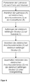
- FIG. 6 shows a flow chart of the inventive method for producing the disc (I) according to the invention with connection element (3).
- the unleaded solder mass (4) portioned and arranged on the contact surface (6) of the electrical connection element (3).
- an electrically conductive structure (2) is applied, for example in the form of printed wires.
- a region of the electrically conductive structure (2) is thereby formed wider so that the dimensions of this region correspond at least to the dimensions of the connection element (3).
- the electrical connection element (3) with the lead-free solder composition (4) is positioned on the electrically conductive structure (2), preferably in its wider-shaped region.
- the lead-free solder mass (4) contacts the electrically conductive structure (2).
- the electrical connection element (3) is permanently electrically and mechanically connected to the electrically conductive structure (2).
Landscapes
- Engineering & Computer Science (AREA)
- Mechanical Engineering (AREA)
- Manufacturing & Machinery (AREA)
- Electric Connection Of Electric Components To Printed Circuits (AREA)
- Connections Effected By Soldering, Adhesion, Or Permanent Deformation (AREA)
- Joining Of Glass To Other Materials (AREA)
- Parts Printed On Printed Circuit Boards (AREA)
- Conductive Materials (AREA)
- Surface Heating Bodies (AREA)
- Resistance Heating (AREA)
Priority Applications (2)
| Application Number | Priority Date | Filing Date | Title |
|---|---|---|---|
| PL13740006T PL2888075T3 (pl) | 2012-08-24 | 2013-07-24 | Szyba z elektrycznym elementem przyłączeniowym |
| EP13740006.5A EP2888075B1 (de) | 2012-08-24 | 2013-07-24 | Scheibe mit elektrischem anschlusselement |
Applications Claiming Priority (3)
| Application Number | Priority Date | Filing Date | Title |
|---|---|---|---|
| EP12181663 | 2012-08-24 | ||
| EP13740006.5A EP2888075B1 (de) | 2012-08-24 | 2013-07-24 | Scheibe mit elektrischem anschlusselement |
| PCT/EP2013/065561 WO2014029576A1 (de) | 2012-08-24 | 2013-07-24 | Scheibe mit elektrischem anschlusselement |
Publications (2)
| Publication Number | Publication Date |
|---|---|
| EP2888075A1 EP2888075A1 (de) | 2015-07-01 |
| EP2888075B1 true EP2888075B1 (de) | 2019-05-08 |
Family
ID=48856627
Family Applications (1)
| Application Number | Title | Priority Date | Filing Date |
|---|---|---|---|
| EP13740006.5A Active EP2888075B1 (de) | 2012-08-24 | 2013-07-24 | Scheibe mit elektrischem anschlusselement |
Country Status (12)
| Country | Link |
|---|---|
| US (1) | US9484651B2 (pl) |
| EP (1) | EP2888075B1 (pl) |
| JP (2) | JP6203262B2 (pl) |
| KR (1) | KR101720888B1 (pl) |
| CN (1) | CN104540636B (pl) |
| BR (1) | BR112015003280B1 (pl) |
| EA (1) | EA028332B1 (pl) |
| ES (1) | ES2740955T3 (pl) |
| MX (1) | MX370004B (pl) |
| PL (1) | PL2888075T3 (pl) |
| TR (1) | TR201910819T4 (pl) |
| WO (1) | WO2014029576A1 (pl) |
Families Citing this family (17)
| Publication number | Priority date | Publication date | Assignee | Title |
|---|---|---|---|---|
| US20140290931A1 (en) * | 2013-04-01 | 2014-10-02 | University Of Maryland, College Park | High Temperature Solder For Downhole Components |
| US10180035B2 (en) | 2013-04-01 | 2019-01-15 | Schlumberger Technology Corporation | Soldered components for downhole use |
| ES2713397T3 (es) * | 2014-10-07 | 2019-05-21 | Saint Gobain | Método de fabricación de un cristal con recubrimiento eléctricamente conductor y una cinta metálica soldada encima; cristal correspondiente |
| JP6826995B2 (ja) * | 2015-05-15 | 2021-02-10 | アプティブ・テクノロジーズ・リミテッド | インジウム−スズ−銀ベースの無鉛はんだ |
| GB201515010D0 (en) * | 2015-08-24 | 2015-10-07 | Pilkington Group Ltd | Electrical connector |
| DE202015007098U1 (de) * | 2015-10-10 | 2017-01-24 | Fractal-Technologies Dr.-Ing. Thomas Reul GmbH | Hybrides-Bleifreies-Elektrisches-Glas-Löt-Anschluß-Element |
| PL3455020T3 (pl) * | 2016-05-10 | 2021-12-20 | Saint-Gobain Glass France | Sposób wytwarzania szyby z elektrycznym elementem przyłączeniowym |
| FR3054403B1 (fr) * | 2016-07-22 | 2019-10-18 | Saint-Gobain Glass France | Vitrage avec element electriquement conducteur et sa connexion electrique |
| CN108788510B (zh) * | 2017-05-03 | 2021-04-16 | 上汽通用汽车有限公司 | 无铅焊料合金及其制备方法和应用、玻璃组件 |
| EP4061094A1 (en) | 2017-11-07 | 2022-09-21 | Central Glass Company, Limited | Car window glass assembly |
| JP7241379B2 (ja) * | 2018-02-08 | 2023-03-17 | 国立研究開発法人産業技術総合研究所 | はんだ実装方法及びマイクロ波加熱装置 |
| GB201804624D0 (en) * | 2018-03-22 | 2018-05-09 | Central Glass Co Ltd | Method of producing a vehicle glass assembly |
| DE102018217612A1 (de) * | 2018-10-15 | 2020-04-16 | Siemens Aktiengesellschaft | Verfahren zur elektrischen Kontaktierung eines supraleitenden Bandleiters |
| JP7078595B2 (ja) * | 2019-11-15 | 2022-05-31 | 矢崎総業株式会社 | 回路体と導電体との接続構造 |
| CN114284770B (zh) * | 2021-12-20 | 2023-04-28 | 福耀玻璃工业集团股份有限公司 | 车用玻璃加热导电组件、车用玻璃及其制作方法 |
| US12269127B2 (en) * | 2022-04-22 | 2025-04-08 | Magna Exteriors, Inc. | Vehicular window assembly process with temperature control of the solder joint that attaches an electrical connector |
| WO2024017966A1 (en) * | 2022-07-19 | 2024-01-25 | Agc Glass Europe | An electrically conductive connector for a window pane |
Family Cites Families (12)
| Publication number | Priority date | Publication date | Assignee | Title |
|---|---|---|---|---|
| US6253988B1 (en) | 1999-03-29 | 2001-07-03 | Antaya Technologies Corporation | Low temperature solder |
| US8169684B2 (en) | 2002-09-30 | 2012-05-01 | Gentex Corporation | Vehicular rearview mirror elements and assemblies incorporating these elements |
| US20060147337A1 (en) | 2003-07-03 | 2006-07-06 | Antaya Technologies Corporation | Solder composition |
| US7159756B2 (en) | 2003-08-29 | 2007-01-09 | Ppg Industries Ohio, Inc. | Method of soldering and solder compositions |
| US20070105412A1 (en) | 2004-11-12 | 2007-05-10 | Agc Automotive Americas R&D, Inc. | Electrical Connector For A Window Pane Of A Vehicle |
| DE102004057630B3 (de) * | 2004-11-30 | 2006-03-30 | Saint-Gobain Sekurit Deutschland Gmbh & Co. Kg | Verfahren und Vorrichtung zum Löten von Anschlüssen mit Induktionswärme |
| EP3590653B1 (en) * | 2005-08-12 | 2023-10-18 | Aptiv Technologies Limited | Solder composition |
| US20080175748A1 (en) * | 2005-08-12 | 2008-07-24 | John Pereira | Solder Composition |
| EP2339894A1 (de) | 2009-12-22 | 2011-06-29 | Saint-Gobain Glass France | Scheibe mit elektrischem Anschlusselement |
| EP2365730A1 (de) * | 2010-03-02 | 2011-09-14 | Saint-Gobain Glass France | Scheibe mit einem elektrischen Anschlusselement |
| JP2011240352A (ja) * | 2010-05-17 | 2011-12-01 | Central Glass Co Ltd | 車両用無鉛はんだ組成物 |
| JP2012091216A (ja) | 2010-10-28 | 2012-05-17 | Asahi Glass Co Ltd | 無鉛はんだ合金、およびこれを用いたガラス物品 |
-
2013
- 2013-07-24 ES ES13740006T patent/ES2740955T3/es active Active
- 2013-07-24 KR KR1020157006976A patent/KR101720888B1/ko not_active Expired - Fee Related
- 2013-07-24 US US14/421,993 patent/US9484651B2/en active Active
- 2013-07-24 MX MX2015002351A patent/MX370004B/es active IP Right Grant
- 2013-07-24 EA EA201590429A patent/EA028332B1/ru not_active IP Right Cessation
- 2013-07-24 EP EP13740006.5A patent/EP2888075B1/de active Active
- 2013-07-24 BR BR112015003280-0A patent/BR112015003280B1/pt not_active IP Right Cessation
- 2013-07-24 JP JP2015527825A patent/JP6203262B2/ja not_active Expired - Fee Related
- 2013-07-24 PL PL13740006T patent/PL2888075T3/pl unknown
- 2013-07-24 WO PCT/EP2013/065561 patent/WO2014029576A1/de not_active Ceased
- 2013-07-24 CN CN201380044442.XA patent/CN104540636B/zh active Active
- 2013-07-24 TR TR2019/10819T patent/TR201910819T4/tr unknown
-
2017
- 2017-01-05 JP JP2017000639A patent/JP2017100190A/ja active Pending
Non-Patent Citations (1)
| Title |
|---|
| SPIEKERMANN P: "LEGIERUNGEN - EIN BESONDERES PATENTRECHTLICHES PROBLEM? - LEGIERUNGSPRUEFUNG IM EUROPAEISCHEN PATENTAMT -", MITTEILUNGEN DER DEUTSCHEN PATENTANWAELTE, HEYMANN, KOLN, DE, 1 January 1993 (1993-01-01), pages 178 - 190, XP000961882, ISSN: 0026-6884 * |
Also Published As
| Publication number | Publication date |
|---|---|
| KR101720888B1 (ko) | 2017-03-28 |
| JP2017100190A (ja) | 2017-06-08 |
| KR20150046191A (ko) | 2015-04-29 |
| EA028332B1 (ru) | 2017-11-30 |
| JP2016500575A (ja) | 2016-01-14 |
| US20150236438A1 (en) | 2015-08-20 |
| EP2888075A1 (de) | 2015-07-01 |
| WO2014029576A1 (de) | 2014-02-27 |
| MX2015002351A (es) | 2015-05-12 |
| TR201910819T4 (tr) | 2019-08-21 |
| ES2740955T3 (es) | 2020-02-07 |
| CN104540636A (zh) | 2015-04-22 |
| JP6203262B2 (ja) | 2017-09-27 |
| PL2888075T3 (pl) | 2019-10-31 |
| MX370004B (es) | 2019-11-28 |
| US9484651B2 (en) | 2016-11-01 |
| CN104540636B (zh) | 2017-09-08 |
| EA201590429A1 (ru) | 2015-06-30 |
| BR112015003280A2 (pt) | 2017-07-04 |
| BR112015003280B1 (pt) | 2020-03-10 |
Similar Documents
| Publication | Publication Date | Title |
|---|---|---|
| EP2888075B1 (de) | Scheibe mit elektrischem anschlusselement | |
| EP2923528B1 (de) | Scheibe mit elektrischem anschlusselement und verbindungssteg | |
| EP2923529B1 (de) | Scheibe mit elektrischem anschlusselement und kompensatorplatten | |
| EP2543229B1 (de) | Scheibe mit einem elektrischen anschlusselement | |
| EP2708091B1 (de) | Scheibe mit einem elektrischen anschlusselement | |
| EP2594109B1 (de) | Scheibe mit einem elektrischen anschlusselement | |
| EP3751960B1 (de) | Scheibe mit einem elektrischen anschlusselement | |
| EP2896269B2 (de) | Scheibe mit einem elektrischen anschlusselement | |
| EP2729277B1 (de) | Verfahren zur herstellung einer scheibe mit einem elektrischen anschlusselement | |
| EP2859620B1 (de) | Scheibe mit einem elektrischen anschlusselement | |
| DE202013006781U1 (de) | Scheibe mit einem elektrischen Anschlusselement | |
| DE202014010271U1 (de) | Scheibe mit mindestens zwei elektrischen Anschlusselementen und Verbindungsleiter |
Legal Events
| Date | Code | Title | Description |
|---|---|---|---|
| PUAI | Public reference made under article 153(3) epc to a published international application that has entered the european phase |
Free format text: ORIGINAL CODE: 0009012 |
|
| 17P | Request for examination filed |
Effective date: 20150204 |
|
| AK | Designated contracting states |
Kind code of ref document: A1 Designated state(s): AL AT BE BG CH CY CZ DE DK EE ES FI FR GB GR HR HU IE IS IT LI LT LU LV MC MK MT NL NO PL PT RO RS SE SI SK SM TR |
|
| AX | Request for extension of the european patent |
Extension state: BA ME |
|
| DAX | Request for extension of the european patent (deleted) | ||
| STAA | Information on the status of an ep patent application or granted ep patent |
Free format text: STATUS: EXAMINATION IS IN PROGRESS |
|
| 17Q | First examination report despatched |
Effective date: 20180403 |
|
| REG | Reference to a national code |
Ref country code: DE Ref legal event code: R079 Ref document number: 502013012801 Country of ref document: DE Free format text: PREVIOUS MAIN CLASS: B23K0035260000 Ipc: B23K0001200000 |
|
| GRAP | Despatch of communication of intention to grant a patent |
Free format text: ORIGINAL CODE: EPIDOSNIGR1 |
|
| STAA | Information on the status of an ep patent application or granted ep patent |
Free format text: STATUS: GRANT OF PATENT IS INTENDED |
|
| RIC1 | Information provided on ipc code assigned before grant |
Ipc: H05B 3/06 20060101ALI20181024BHEP Ipc: B23K 35/26 20060101ALI20181024BHEP Ipc: H01R 13/02 20060101ALI20181024BHEP Ipc: H05B 3/84 20060101ALI20181024BHEP Ipc: B23K 1/20 20060101AFI20181024BHEP Ipc: B23K 1/00 20060101ALI20181024BHEP Ipc: H01R 43/02 20060101ALI20181024BHEP |
|
| INTG | Intention to grant announced |
Effective date: 20181115 |
|
| RIN1 | Information on inventor provided before grant (corrected) |
Inventor name: REUL, BERNHARD Inventor name: RATEICZAK, MITJA Inventor name: SCHMALBUCH, KLAUS |
|
| GRAS | Grant fee paid |
Free format text: ORIGINAL CODE: EPIDOSNIGR3 |
|
| GRAA | (expected) grant |
Free format text: ORIGINAL CODE: 0009210 |
|
| STAA | Information on the status of an ep patent application or granted ep patent |
Free format text: STATUS: THE PATENT HAS BEEN GRANTED |
|
| AK | Designated contracting states |
Kind code of ref document: B1 Designated state(s): AL AT BE BG CH CY CZ DE DK EE ES FI FR GB GR HR HU IE IS IT LI LT LU LV MC MK MT NL NO PL PT RO RS SE SI SK SM TR |
|
| REG | Reference to a national code |
Ref country code: GB Ref legal event code: FG4D Free format text: NOT ENGLISH |
|
| REG | Reference to a national code |
Ref country code: CH Ref legal event code: EP Ref country code: AT Ref legal event code: REF Ref document number: 1129427 Country of ref document: AT Kind code of ref document: T Effective date: 20190515 |
|
| REG | Reference to a national code |
Ref country code: DE Ref legal event code: R096 Ref document number: 502013012801 Country of ref document: DE |
|
| REG | Reference to a national code |
Ref country code: IE Ref legal event code: FG4D Free format text: LANGUAGE OF EP DOCUMENT: GERMAN |
|
| REG | Reference to a national code |
Ref country code: RO Ref legal event code: EPE |
|
| REG | Reference to a national code |
Ref country code: NL Ref legal event code: FP |
|
| REG | Reference to a national code |
Ref country code: SE Ref legal event code: TRGR |
|
| PGFP | Annual fee paid to national office [announced via postgrant information from national office to epo] |
Ref country code: NL Payment date: 20190712 Year of fee payment: 7 |
|
| REG | Reference to a national code |
Ref country code: LT Ref legal event code: MG4D |
|
| PG25 | Lapsed in a contracting state [announced via postgrant information from national office to epo] |
Ref country code: AL Free format text: LAPSE BECAUSE OF FAILURE TO SUBMIT A TRANSLATION OF THE DESCRIPTION OR TO PAY THE FEE WITHIN THE PRESCRIBED TIME-LIMIT Effective date: 20190508 Ref country code: PT Free format text: LAPSE BECAUSE OF FAILURE TO SUBMIT A TRANSLATION OF THE DESCRIPTION OR TO PAY THE FEE WITHIN THE PRESCRIBED TIME-LIMIT Effective date: 20190908 Ref country code: FI Free format text: LAPSE BECAUSE OF FAILURE TO SUBMIT A TRANSLATION OF THE DESCRIPTION OR TO PAY THE FEE WITHIN THE PRESCRIBED TIME-LIMIT Effective date: 20190508 Ref country code: NO Free format text: LAPSE BECAUSE OF FAILURE TO SUBMIT A TRANSLATION OF THE DESCRIPTION OR TO PAY THE FEE WITHIN THE PRESCRIBED TIME-LIMIT Effective date: 20190808 Ref country code: HR Free format text: LAPSE BECAUSE OF FAILURE TO SUBMIT A TRANSLATION OF THE DESCRIPTION OR TO PAY THE FEE WITHIN THE PRESCRIBED TIME-LIMIT Effective date: 20190508 Ref country code: LT Free format text: LAPSE BECAUSE OF FAILURE TO SUBMIT A TRANSLATION OF THE DESCRIPTION OR TO PAY THE FEE WITHIN THE PRESCRIBED TIME-LIMIT Effective date: 20190508 |
|
| PGFP | Annual fee paid to national office [announced via postgrant information from national office to epo] |
Ref country code: GB Payment date: 20190627 Year of fee payment: 7 Ref country code: ES Payment date: 20190801 Year of fee payment: 7 Ref country code: DE Payment date: 20190716 Year of fee payment: 7 |
|
| PG25 | Lapsed in a contracting state [announced via postgrant information from national office to epo] |
Ref country code: RS Free format text: LAPSE BECAUSE OF FAILURE TO SUBMIT A TRANSLATION OF THE DESCRIPTION OR TO PAY THE FEE WITHIN THE PRESCRIBED TIME-LIMIT Effective date: 20190508 Ref country code: BG Free format text: LAPSE BECAUSE OF FAILURE TO SUBMIT A TRANSLATION OF THE DESCRIPTION OR TO PAY THE FEE WITHIN THE PRESCRIBED TIME-LIMIT Effective date: 20190808 Ref country code: GR Free format text: LAPSE BECAUSE OF FAILURE TO SUBMIT A TRANSLATION OF THE DESCRIPTION OR TO PAY THE FEE WITHIN THE PRESCRIBED TIME-LIMIT Effective date: 20190809 Ref country code: LV Free format text: LAPSE BECAUSE OF FAILURE TO SUBMIT A TRANSLATION OF THE DESCRIPTION OR TO PAY THE FEE WITHIN THE PRESCRIBED TIME-LIMIT Effective date: 20190508 |
|
| PGFP | Annual fee paid to national office [announced via postgrant information from national office to epo] |
Ref country code: GB Payment date: 20190724 Year of fee payment: 7 |
|
| REG | Reference to a national code |
Ref country code: SK Ref legal event code: T3 Ref document number: E 32374 Country of ref document: SK |
|
| PG25 | Lapsed in a contracting state [announced via postgrant information from national office to epo] |
Ref country code: CZ Free format text: LAPSE BECAUSE OF FAILURE TO SUBMIT A TRANSLATION OF THE DESCRIPTION OR TO PAY THE FEE WITHIN THE PRESCRIBED TIME-LIMIT Effective date: 20190508 Ref country code: DK Free format text: LAPSE BECAUSE OF FAILURE TO SUBMIT A TRANSLATION OF THE DESCRIPTION OR TO PAY THE FEE WITHIN THE PRESCRIBED TIME-LIMIT Effective date: 20190508 Ref country code: EE Free format text: LAPSE BECAUSE OF FAILURE TO SUBMIT A TRANSLATION OF THE DESCRIPTION OR TO PAY THE FEE WITHIN THE PRESCRIBED TIME-LIMIT Effective date: 20190508 |
|
| REG | Reference to a national code |
Ref country code: ES Ref legal event code: FG2A Ref document number: 2740955 Country of ref document: ES Kind code of ref document: T3 Effective date: 20200207 |
|
| REG | Reference to a national code |
Ref country code: DE Ref legal event code: R097 Ref document number: 502013012801 Country of ref document: DE |
|
| PG25 | Lapsed in a contracting state [announced via postgrant information from national office to epo] |
Ref country code: MC Free format text: LAPSE BECAUSE OF FAILURE TO SUBMIT A TRANSLATION OF THE DESCRIPTION OR TO PAY THE FEE WITHIN THE PRESCRIBED TIME-LIMIT Effective date: 20190508 Ref country code: SM Free format text: LAPSE BECAUSE OF FAILURE TO SUBMIT A TRANSLATION OF THE DESCRIPTION OR TO PAY THE FEE WITHIN THE PRESCRIBED TIME-LIMIT Effective date: 20190508 |
|
| REG | Reference to a national code |
Ref country code: CH Ref legal event code: PL |
|
| PLBE | No opposition filed within time limit |
Free format text: ORIGINAL CODE: 0009261 |
|
| STAA | Information on the status of an ep patent application or granted ep patent |
Free format text: STATUS: NO OPPOSITION FILED WITHIN TIME LIMIT |
|
| 26N | No opposition filed |
Effective date: 20200211 |
|
| PG25 | Lapsed in a contracting state [announced via postgrant information from national office to epo] |
Ref country code: SI Free format text: LAPSE BECAUSE OF FAILURE TO SUBMIT A TRANSLATION OF THE DESCRIPTION OR TO PAY THE FEE WITHIN THE PRESCRIBED TIME-LIMIT Effective date: 20190508 Ref country code: LI Free format text: LAPSE BECAUSE OF NON-PAYMENT OF DUE FEES Effective date: 20190731 Ref country code: LU Free format text: LAPSE BECAUSE OF NON-PAYMENT OF DUE FEES Effective date: 20190724 Ref country code: CH Free format text: LAPSE BECAUSE OF NON-PAYMENT OF DUE FEES Effective date: 20190731 |
|
| PG25 | Lapsed in a contracting state [announced via postgrant information from national office to epo] |
Ref country code: IE Free format text: LAPSE BECAUSE OF NON-PAYMENT OF DUE FEES Effective date: 20190724 |
|
| PGFP | Annual fee paid to national office [announced via postgrant information from national office to epo] |
Ref country code: BE Payment date: 20200617 Year of fee payment: 8 |
|
| REG | Reference to a national code |
Ref country code: AT Ref legal event code: MM01 Ref document number: 1129427 Country of ref document: AT Kind code of ref document: T Effective date: 20190724 |
|
| PG25 | Lapsed in a contracting state [announced via postgrant information from national office to epo] |
Ref country code: AT Free format text: LAPSE BECAUSE OF NON-PAYMENT OF DUE FEES Effective date: 20190724 |
|
| REG | Reference to a national code |
Ref country code: DE Ref legal event code: R119 Ref document number: 502013012801 Country of ref document: DE |
|
| REG | Reference to a national code |
Ref country code: SE Ref legal event code: EUG |
|
| REG | Reference to a national code |
Ref country code: NL Ref legal event code: MM Effective date: 20200801 |
|
| GBPC | Gb: european patent ceased through non-payment of renewal fee |
Effective date: 20200724 |
|
| PG25 | Lapsed in a contracting state [announced via postgrant information from national office to epo] |
Ref country code: NL Free format text: LAPSE BECAUSE OF NON-PAYMENT OF DUE FEES Effective date: 20200801 Ref country code: GB Free format text: LAPSE BECAUSE OF NON-PAYMENT OF DUE FEES Effective date: 20200724 |
|
| PG25 | Lapsed in a contracting state [announced via postgrant information from national office to epo] |
Ref country code: CY Free format text: LAPSE BECAUSE OF FAILURE TO SUBMIT A TRANSLATION OF THE DESCRIPTION OR TO PAY THE FEE WITHIN THE PRESCRIBED TIME-LIMIT Effective date: 20190508 Ref country code: DE Free format text: LAPSE BECAUSE OF NON-PAYMENT OF DUE FEES Effective date: 20210202 Ref country code: SE Free format text: LAPSE BECAUSE OF NON-PAYMENT OF DUE FEES Effective date: 20200725 |
|
| PG25 | Lapsed in a contracting state [announced via postgrant information from national office to epo] |
Ref country code: IS Free format text: LAPSE BECAUSE OF FAILURE TO SUBMIT A TRANSLATION OF THE DESCRIPTION OR TO PAY THE FEE WITHIN THE PRESCRIBED TIME-LIMIT Effective date: 20190908 |
|
| PG25 | Lapsed in a contracting state [announced via postgrant information from national office to epo] |
Ref country code: MT Free format text: LAPSE BECAUSE OF FAILURE TO SUBMIT A TRANSLATION OF THE DESCRIPTION OR TO PAY THE FEE WITHIN THE PRESCRIBED TIME-LIMIT Effective date: 20190508 Ref country code: HU Free format text: LAPSE BECAUSE OF FAILURE TO SUBMIT A TRANSLATION OF THE DESCRIPTION OR TO PAY THE FEE WITHIN THE PRESCRIBED TIME-LIMIT; INVALID AB INITIO Effective date: 20130724 |
|
| REG | Reference to a national code |
Ref country code: ES Ref legal event code: FD2A Effective date: 20211230 |
|
| PG25 | Lapsed in a contracting state [announced via postgrant information from national office to epo] |
Ref country code: ES Free format text: LAPSE BECAUSE OF NON-PAYMENT OF DUE FEES Effective date: 20200725 |
|
| REG | Reference to a national code |
Ref country code: BE Ref legal event code: MM Effective date: 20210731 |
|
| PG25 | Lapsed in a contracting state [announced via postgrant information from national office to epo] |
Ref country code: MK Free format text: LAPSE BECAUSE OF FAILURE TO SUBMIT A TRANSLATION OF THE DESCRIPTION OR TO PAY THE FEE WITHIN THE PRESCRIBED TIME-LIMIT Effective date: 20190508 |
|
| PG25 | Lapsed in a contracting state [announced via postgrant information from national office to epo] |
Ref country code: BE Free format text: LAPSE BECAUSE OF NON-PAYMENT OF DUE FEES Effective date: 20210731 |
|
| REG | Reference to a national code |
Ref country code: SK Ref legal event code: PC4A Ref document number: E 32374 Country of ref document: SK Owner name: SAINT-GOBAIN SEKURIT FRANCE, THOUROTTE, FR Free format text: FORMER OWNER: SAINT-GOBAIN GLASS FRANCE, COURBEVOIE, FR Effective date: 20250522 |
|
| PGFP | Annual fee paid to national office [announced via postgrant information from national office to epo] |
Ref country code: PL Payment date: 20250611 Year of fee payment: 13 |
|
| PGFP | Annual fee paid to national office [announced via postgrant information from national office to epo] |
Ref country code: FR Payment date: 20250610 Year of fee payment: 13 |
|
| PGFP | Annual fee paid to national office [announced via postgrant information from national office to epo] |
Ref country code: RO Payment date: 20250625 Year of fee payment: 13 |
|
| PGFP | Annual fee paid to national office [announced via postgrant information from national office to epo] |
Ref country code: SK Payment date: 20250612 Year of fee payment: 13 |
|
| PGFP | Annual fee paid to national office [announced via postgrant information from national office to epo] |
Ref country code: TR Payment date: 20250709 Year of fee payment: 13 Ref country code: IT Payment date: 20250623 Year of fee payment: 13 |