EP3590653B1 - Solder composition - Google Patents
Solder composition Download PDFInfo
- Publication number
- EP3590653B1 EP3590653B1 EP19193508.9A EP19193508A EP3590653B1 EP 3590653 B1 EP3590653 B1 EP 3590653B1 EP 19193508 A EP19193508 A EP 19193508A EP 3590653 B1 EP3590653 B1 EP 3590653B1
- Authority
- EP
- European Patent Office
- Prior art keywords
- solder
- tin
- indium
- composition
- silver
- Prior art date
- Legal status (The legal status is an assumption and is not a legal conclusion. Google has not performed a legal analysis and makes no representation as to the accuracy of the status listed.)
- Active
Links
- 229910000679 solder Inorganic materials 0.000 title claims description 253
- 239000000203 mixture Substances 0.000 title claims description 92
- 229910052718 tin Inorganic materials 0.000 claims description 66
- ATJFFYVFTNAWJD-UHFFFAOYSA-N Tin Chemical compound [Sn] ATJFFYVFTNAWJD-UHFFFAOYSA-N 0.000 claims description 59
- 229910052738 indium Inorganic materials 0.000 claims description 52
- 229910052709 silver Inorganic materials 0.000 claims description 52
- APFVFJFRJDLVQX-UHFFFAOYSA-N indium atom Chemical compound [In] APFVFJFRJDLVQX-UHFFFAOYSA-N 0.000 claims description 51
- 239000010949 copper Substances 0.000 claims description 44
- 239000004332 silver Substances 0.000 claims description 44
- 229910052802 copper Inorganic materials 0.000 claims description 40
- RYGMFSIKBFXOCR-UHFFFAOYSA-N Copper Chemical compound [Cu] RYGMFSIKBFXOCR-UHFFFAOYSA-N 0.000 claims description 36
- 229910052797 bismuth Inorganic materials 0.000 claims description 31
- JCXGWMGPZLAOME-UHFFFAOYSA-N bismuth atom Chemical compound [Bi] JCXGWMGPZLAOME-UHFFFAOYSA-N 0.000 claims description 31
- 238000002844 melting Methods 0.000 description 56
- 230000008018 melting Effects 0.000 description 56
- 239000011521 glass Substances 0.000 description 51
- BQCADISMDOOEFD-UHFFFAOYSA-N Silver Chemical compound [Ag] BQCADISMDOOEFD-UHFFFAOYSA-N 0.000 description 37
- 239000000758 substrate Substances 0.000 description 35
- 238000005476 soldering Methods 0.000 description 30
- 238000005096 rolling process Methods 0.000 description 16
- 238000005336 cracking Methods 0.000 description 12
- 238000005097 cold rolling Methods 0.000 description 8
- 239000000463 material Substances 0.000 description 8
- 238000000034 method Methods 0.000 description 7
- 230000008569 process Effects 0.000 description 7
- 238000009966 trimming Methods 0.000 description 7
- 238000001816 cooling Methods 0.000 description 5
- 238000010438 heat treatment Methods 0.000 description 5
- 238000004901 spalling Methods 0.000 description 5
- XEEYBQQBJWHFJM-UHFFFAOYSA-N Iron Chemical compound [Fe] XEEYBQQBJWHFJM-UHFFFAOYSA-N 0.000 description 4
- 230000004907 flux Effects 0.000 description 4
- 230000013011 mating Effects 0.000 description 3
- PXHVJJICTQNCMI-UHFFFAOYSA-N Nickel Chemical compound [Ni] PXHVJJICTQNCMI-UHFFFAOYSA-N 0.000 description 2
- XUIMIQQOPSSXEZ-UHFFFAOYSA-N Silicon Chemical compound [Si] XUIMIQQOPSSXEZ-UHFFFAOYSA-N 0.000 description 2
- 239000000919 ceramic Substances 0.000 description 2
- 229910052742 iron Inorganic materials 0.000 description 2
- 238000004519 manufacturing process Methods 0.000 description 2
- 229910052751 metal Inorganic materials 0.000 description 2
- 239000002184 metal Substances 0.000 description 2
- 239000000843 powder Substances 0.000 description 2
- 230000009467 reduction Effects 0.000 description 2
- 230000002000 scavenging effect Effects 0.000 description 2
- 229910052710 silicon Inorganic materials 0.000 description 2
- 239000010703 silicon Substances 0.000 description 2
- 239000000126 substance Substances 0.000 description 2
- 238000010257 thawing Methods 0.000 description 2
- 230000008646 thermal stress Effects 0.000 description 2
- 238000003466 welding Methods 0.000 description 2
- 241000220010 Rhode Species 0.000 description 1
- 229910000831 Steel Inorganic materials 0.000 description 1
- HCHKCACWOHOZIP-UHFFFAOYSA-N Zinc Chemical compound [Zn] HCHKCACWOHOZIP-UHFFFAOYSA-N 0.000 description 1
- -1 about 97% Sn 3% Ag Chemical compound 0.000 description 1
- 229910052782 aluminium Inorganic materials 0.000 description 1
- XAGFODPZIPBFFR-UHFFFAOYSA-N aluminium Chemical compound [Al] XAGFODPZIPBFFR-UHFFFAOYSA-N 0.000 description 1
- 229910052787 antimony Inorganic materials 0.000 description 1
- WATWJIUSRGPENY-UHFFFAOYSA-N antimony atom Chemical compound [Sb] WATWJIUSRGPENY-UHFFFAOYSA-N 0.000 description 1
- 229910052785 arsenic Inorganic materials 0.000 description 1
- RQNWIZPPADIBDY-UHFFFAOYSA-N arsenic atom Chemical compound [As] RQNWIZPPADIBDY-UHFFFAOYSA-N 0.000 description 1
- 229910052793 cadmium Inorganic materials 0.000 description 1
- BDOSMKKIYDKNTQ-UHFFFAOYSA-N cadmium atom Chemical compound [Cd] BDOSMKKIYDKNTQ-UHFFFAOYSA-N 0.000 description 1
- 230000008859 change Effects 0.000 description 1
- 239000011248 coating agent Substances 0.000 description 1
- 238000000576 coating method Methods 0.000 description 1
- 239000000356 contaminant Substances 0.000 description 1
- 230000001419 dependent effect Effects 0.000 description 1
- 230000008021 deposition Effects 0.000 description 1
- 238000005516 engineering process Methods 0.000 description 1
- 230000007613 environmental effect Effects 0.000 description 1
- PCHJSUWPFVWCPO-UHFFFAOYSA-N gold Chemical compound [Au] PCHJSUWPFVWCPO-UHFFFAOYSA-N 0.000 description 1
- 229910052737 gold Inorganic materials 0.000 description 1
- 239000010931 gold Substances 0.000 description 1
- 238000003754 machining Methods 0.000 description 1
- 230000005012 migration Effects 0.000 description 1
- 238000013508 migration Methods 0.000 description 1
- 238000002156 mixing Methods 0.000 description 1
- 229910052759 nickel Inorganic materials 0.000 description 1
- 238000007711 solidification Methods 0.000 description 1
- 230000008023 solidification Effects 0.000 description 1
- 239000010959 steel Substances 0.000 description 1
- 230000035882 stress Effects 0.000 description 1
- 238000011282 treatment Methods 0.000 description 1
- 238000009736 wetting Methods 0.000 description 1
- 229910052725 zinc Inorganic materials 0.000 description 1
- 239000011701 zinc Substances 0.000 description 1
Images

Classifications
-
- C—CHEMISTRY; METALLURGY
- C22—METALLURGY; FERROUS OR NON-FERROUS ALLOYS; TREATMENT OF ALLOYS OR NON-FERROUS METALS
- C22C—ALLOYS
- C22C13/00—Alloys based on tin
-
- B—PERFORMING OPERATIONS; TRANSPORTING
- B23—MACHINE TOOLS; METAL-WORKING NOT OTHERWISE PROVIDED FOR
- B23K—SOLDERING OR UNSOLDERING; WELDING; CLADDING OR PLATING BY SOLDERING OR WELDING; CUTTING BY APPLYING HEAT LOCALLY, e.g. FLAME CUTTING; WORKING BY LASER BEAM
- B23K35/00—Rods, electrodes, materials, or media, for use in soldering, welding, or cutting
- B23K35/02—Rods, electrodes, materials, or media, for use in soldering, welding, or cutting characterised by mechanical features, e.g. shape
- B23K35/0222—Rods, electrodes, materials, or media, for use in soldering, welding, or cutting characterised by mechanical features, e.g. shape for use in soldering, brazing
- B23K35/0233—Sheets, foils
- B23K35/0238—Sheets, foils layered
-
- B—PERFORMING OPERATIONS; TRANSPORTING
- B23—MACHINE TOOLS; METAL-WORKING NOT OTHERWISE PROVIDED FOR
- B23K—SOLDERING OR UNSOLDERING; WELDING; CLADDING OR PLATING BY SOLDERING OR WELDING; CUTTING BY APPLYING HEAT LOCALLY, e.g. FLAME CUTTING; WORKING BY LASER BEAM
- B23K35/00—Rods, electrodes, materials, or media, for use in soldering, welding, or cutting
- B23K35/22—Rods, electrodes, materials, or media, for use in soldering, welding, or cutting characterised by the composition or nature of the material
- B23K35/24—Selection of soldering or welding materials proper
- B23K35/26—Selection of soldering or welding materials proper with the principal constituent melting at less than 400 degrees C
- B23K35/262—Sn as the principal constituent
-
- B—PERFORMING OPERATIONS; TRANSPORTING
- B23—MACHINE TOOLS; METAL-WORKING NOT OTHERWISE PROVIDED FOR
- B23K—SOLDERING OR UNSOLDERING; WELDING; CLADDING OR PLATING BY SOLDERING OR WELDING; CUTTING BY APPLYING HEAT LOCALLY, e.g. FLAME CUTTING; WORKING BY LASER BEAM
- B23K35/00—Rods, electrodes, materials, or media, for use in soldering, welding, or cutting
- B23K35/22—Rods, electrodes, materials, or media, for use in soldering, welding, or cutting characterised by the composition or nature of the material
- B23K35/24—Selection of soldering or welding materials proper
- B23K35/30—Selection of soldering or welding materials proper with the principal constituent melting at less than 1550 degrees C
- B23K35/302—Cu as the principal constituent
-
- B—PERFORMING OPERATIONS; TRANSPORTING
- B32—LAYERED PRODUCTS
- B32B—LAYERED PRODUCTS, i.e. PRODUCTS BUILT-UP OF STRATA OF FLAT OR NON-FLAT, e.g. CELLULAR OR HONEYCOMB, FORM
- B32B15/00—Layered products comprising a layer of metal
- B32B15/01—Layered products comprising a layer of metal all layers being exclusively metallic
-
- C—CHEMISTRY; METALLURGY
- C03—GLASS; MINERAL OR SLAG WOOL
- C03C—CHEMICAL COMPOSITION OF GLASSES, GLAZES OR VITREOUS ENAMELS; SURFACE TREATMENT OF GLASS; SURFACE TREATMENT OF FIBRES OR FILAMENTS MADE FROM GLASS, MINERALS OR SLAGS; JOINING GLASS TO GLASS OR OTHER MATERIALS
- C03C17/00—Surface treatment of glass, not in the form of fibres or filaments, by coating
- C03C17/34—Surface treatment of glass, not in the form of fibres or filaments, by coating with at least two coatings having different compositions
- C03C17/36—Surface treatment of glass, not in the form of fibres or filaments, by coating with at least two coatings having different compositions at least one coating being a metal
- C03C17/3602—Surface treatment of glass, not in the form of fibres or filaments, by coating with at least two coatings having different compositions at least one coating being a metal the metal being present as a layer
- C03C17/3668—Surface treatment of glass, not in the form of fibres or filaments, by coating with at least two coatings having different compositions at least one coating being a metal the metal being present as a layer the multilayer coating having electrical properties
- C03C17/3673—Surface treatment of glass, not in the form of fibres or filaments, by coating with at least two coatings having different compositions at least one coating being a metal the metal being present as a layer the multilayer coating having electrical properties specially adapted for use in heating devices for rear window of vehicles
-
- C—CHEMISTRY; METALLURGY
- C03—GLASS; MINERAL OR SLAG WOOL
- C03C—CHEMICAL COMPOSITION OF GLASSES, GLAZES OR VITREOUS ENAMELS; SURFACE TREATMENT OF GLASS; SURFACE TREATMENT OF FIBRES OR FILAMENTS MADE FROM GLASS, MINERALS OR SLAGS; JOINING GLASS TO GLASS OR OTHER MATERIALS
- C03C27/00—Joining pieces of glass to pieces of other inorganic material; Joining glass to glass other than by fusing
- C03C27/04—Joining glass to metal by means of an interlayer
- C03C27/042—Joining glass to metal by means of an interlayer consisting of a combination of materials selected from glass, glass-ceramic or ceramic material with metals, metal oxides or metal salts
- C03C27/046—Joining glass to metal by means of an interlayer consisting of a combination of materials selected from glass, glass-ceramic or ceramic material with metals, metal oxides or metal salts of metals, metal oxides or metal salts only
-
- C—CHEMISTRY; METALLURGY
- C22—METALLURGY; FERROUS OR NON-FERROUS ALLOYS; TREATMENT OF ALLOYS OR NON-FERROUS METALS
- C22C—ALLOYS
- C22C28/00—Alloys based on a metal not provided for in groups C22C5/00 - C22C27/00
-
- C—CHEMISTRY; METALLURGY
- C22—METALLURGY; FERROUS OR NON-FERROUS ALLOYS; TREATMENT OF ALLOYS OR NON-FERROUS METALS
- C22C—ALLOYS
- C22C30/00—Alloys containing less than 50% by weight of each constituent
- C22C30/04—Alloys containing less than 50% by weight of each constituent containing tin or lead
Definitions
- Electrical connectors are typically used for making electrical connections to devices such as antennas and defrosters, which are incorporated on or embedded within automotive glass.
- the electrical connectors are commonly soldered to the glass with a solder that contains lead. Due to environmental concerns, most industries are currently using or planning to use low or non-lead solders for various soldering applications.
- a common non-lead solder employed in some industries contains a high tin (Sn) content, for example 95% tin.
- Sn tin
- Automotive glass tends to be brittle, and the common high tin, non-lead solders that are suitable for use in other applications can typically cause cracking of the automotive glass.
- materials such as ceramics and silicon might appear to be similar in some respects to automotive glass, some solders that are suitable for soldering to ceramic or silicon devices are not suitable for soldering to automotive glass.
- Publication WO 00/58051 A discloses a low temperature solder composition having about 65% indium, 30% tin, 4.5 % silver, and 0.5 % copper by weight.
- the solder composition can also contain trace amounts of antimony, gold, lead, aluminum, arsenic, cadmium, zinc, bismuth, iron or nickel.
- Publication " Solder for soldering components of electrovacuum devices" discloses a solder composition comprising indium, 0.05-12% Ag, 35-60% Sn, and 0.5-5% Cu.
- the present invention provides a solder article that can be suitable for soldering to automotive glass and can be lead free.
- a solder composition according to the present invention discloses the features of claim 1. Preferred embodiments are described in the dependent claims.
- FIG. 1 depicts an embodiment of an apparatus 10 for forming a multilayer solder article 24 ( FIG. 6 ).
- the multilayer solder article 24 can have a multilayer solder 15 which can include a first solder 13 and a second solder 16.
- a clad ribbon, strip, belt or band 12 FIG. 4
- the first solder 13 can be a higher melting point or temperature solder.
- the base substrate 11 can be a ribbon, strip, belt or band of sheet metal suitable for forming electrical devices, such as electrical connectors, by stamping.
- the clad band 12 can be moved through a guide 20 to align the clad band 12 with a rolling device or mill 14 ( FIG. 2 ).
- a ribbon, strip, belt or band 16b of a second or lower melting point or temperature solder 16 can be pulled from a roll 16a at an unwind station for positioning on or over the higher melting temperature solder 13.
- the second solder 16 can be softer or more ductile than the first solder 13.
- the band 16b of the second solder 16 can be moved through the guide 20 ( FIG. 3 ) for alignment with both the clad band 12 and the rolling mill 14.
- the guide 20 can align the band 16b of the second solder 16 relative to or with the first solder 13 and the base substrate 11.
- the band 16b of the second solder 16 and the clad band 12 can be cold rolled together by rolling mill 14 between first or upper 18 a, and second or lower 18b rollers of a roll system 18. Cold rolling can combine or bond the second solder 16 with the first solder 13 to form the multilayer solder article 24.
- a heating station 26 can be positioned after the rolling mill 14 for heating the multilayer solder article 24 to ensure a sufficient bond between the first solder 13 and the second solder 16, but without melting the solders 13 or 16.
- the heating station 26 can be a flame heater positioned under the base substrate 11 as shown, or in other embodiments, can be an oven, hot air gun, etc.
- the multilayer solder article 24 ( FIG. 6 ) can then be wound up in a roll 24a at a windup station.
- the guide 20 can be secured to the rolling mill 14 close to the rollers 18a/18b.
- the position of the guide 20 can be adjusted by an adjustment device 22 ( FIG. 1 ).
- the guide 20 can include a first or upper portion 32 and a second or lower portion 34 which are shaped and fastened together to form a longitudinal passage 36 through the guide 20 ( FIG. 3 ).
- the lower portion 34 can have a groove 34a which is sized to guide the base substrate 11 through the guide 20 and the upper portion 32 can have a groove 32a which is sized and positioned for guiding the band 16b of the second solder 16 in alignment with the first solder 13 on the base substrate 11.
- the guide 20 can commence the combining of the second solder 16 with the first solder 13 and the base substrate 11.
- the downstream end of the guide 20 can be contoured such as in a tapered or curved manner in order to be positioned closely between and adjacent to rolls 18a and 18b.
- the groove 34a can be about .01 inches (0.025 cm) wider and .004 inches (0.010 cm) higher than the width and thickness of the base substrate 11.
- the groove 32a can be about .025 inches (0.063 cm) wider than the width of the solder 13 on the base substrate 11 and about .010 inches (0.254 cm) higher than the combined height or thicknesses of the first solder 13 and the band 16b of the second solder 16.
- the rolling mill 14 can include a frame 30 to which the rolls 18a and 18b are rotatably mounted about first or upper 17a, and second or lower 17b axes, respectively.
- a gear system 28 can be connected to the roller system 18 for causing the rolls 18a and 18b to rotate in unison.
- the gear system 28 can include a first or upper gear 28a that is secured to roll 18a along axis 17a, and a second or lower gear 28b that is secured to roll 18b along axis 17b.
- Gears 28a and 28b can be engaged or intermeshed with each other.
- the rolling mill 14 can be driven by a motor drive 29, or can be rotated by the movement of the clad band 12 and the second solder 16 passing between the rolls 18a and 18b.
- the space 35 between the rolls 18a and 18b can be adjusted by an adjustment fixture 33 to provide the desired amount of pressure on the clad band 12 and solder 16 during the rolling process in order to bond the second solder 16 to the first solder 13 by cold rolling.
- the space 35 between rolls 18a and 18b can be set to reduce the initial combined height or thickness of the first solder 13 and the second solder 16 by about 30% to 50%.
- the adjustment fixture 33 can include a pair of cylinders 31, for example, hydraulic or pneumatic cylinders, for positioning roll 18a and axis 17a relative to roll 18b and axis 17b, and providing rolling pressure.
- the cylinders 31 can be secured to an adjustable plate 37, which can be adjusted, for example, with adjustment screws (not shown) to change the position of the cylinders 31.
- the cold rolling by rolling mill 14 can be performed without requiring pretreatment of the mating surfaces of the first 13 and second 16 solders (for example, the removal of contaminants such as oxides, by chemical, energy or mechanical means).
- the thickness reduction and material deformation of the first 13 and second 16 solders during the cold rolling process can provide sufficient pressure, heat or material changes for bonding to occur between the layers of the first 13 and second 16 solders.
- the heating station 26 can be omitted.
- the base substrate 11 can be omitted so that the first 13 and second 16 solders are alone combined by the rolling mill 14 to form a multilayer solder article.
- the guide 20 can be modified to accommodate the omission of the base substrate 11.
- the band 9 of the first solder 13 can initially be about .016 inches (0.041 cm) thick and the thickness of the first solder 13 can be reduced to about .005 to .010 inches (0.013 to 0.025 cm) thick by trimming, machining or skiving. Thickness reduction can also include cold rolling.
- the band 16b of the second solder 16 can initially be about .010 inches (0.025 cm) thick and the thickness of the second solder 16 can be reduced to about .005 to .008 inches (0.013 to 0.020 cm) thick by trimming and/or cold rolling.
- the total thickness of multilayer solder 15 can be about .013 to .015 inches (0.033 to 0.038 cm) thick, In some embodiments, the multilayer solder 15 can be about .007 to .040 inches (0.018 to 0,102 cm) thick. In other embodiments, solder 13 can be even thinner or omitted, and the layer of the second solder 16 can range between about .001 to .008 inches (0.003 to 0.020 cm) thick. Depending upon the application at hand, the thicknesses can be even higher or lower than those described above. The second solder 16 can be softer and more ductile than the first solder 13. In particular embodiments, the multilayer solder 15 can be formed of generally lead free compositions that are suitable for cold rolling by the rolling mill 14 of apparatus 10.
- the clad band 12 can be pre-formed prior to being processed by apparatus 10. This can be accomplished by embodiments of the apparatus 8 depicted in FIG. 5 where a moving band of the base substrate 11 can have flux 46a applied to a surface of the base substrate 11 at a flux station 46, such as by a brush, roller dispenser, etc.
- a ribbon, strip, belt or band 9 of the first or higher melting temperature solder 13 can be applied by a roller 48 over the flux 46a and against the base substrate 11.
- the band 9 of the first solder 13 can then be melted or reflowed at a heating station 50, such as by flames, oven, hot air gun, etc., to melt and bond the band 9 to the base substrate 11 as reflowed solder 9a.
- a skiving or trimming station 52 can be included for trimming the reflowed solder 9a and/or the base substrate 11 to result in clad band 12 with a trimmed layer 9b of the first or higher melting temperature solder 13 at desired dimensions.
- the desired dimensions can be thickness and/or width.
- the trimming can also be performed on a separate processing machine.
- the clad band 12 can be wound up in a roll 12a for processing on apparatus 10.
- the clad band 12 can be fed directly into rolling mill 14 for combining with the band 16b of the second solder 16.
- the multilayer solder article 24 produced by apparatus 10 can have a multilayer solder 15 where the first or higher melting temperature solder 13 can be positioned or bonded against the base substrate 11 and the second or higher melting temperature solder 16 can be bonded over the first solder 13.
- the multilayer solder 15 can be a strip that is narrower than the base substrate 11 and can be located along a longitudinal axis of the base substrate 11, for example, the central longitudinal axis. As a result, only a portion of the base substrate 11 can be covered by the multilayer solder 15 so that side margins of the base substrate 11 are exposed.
- the base substrate 11 can be made of a material, such as sheet metal that is suitable for forming into electrical devices.
- base substrate 11 can be made of copper, for example, C110 that is about .031 inches (0.079 cm) thick and about 1.812 inches (4.602 cm) wide.
- the base substrate 11 can be trimmed down to a width of about 1.56 inches (3.962 cm).
- the multilayer solder 15 can be about .620 inches (1.575 cm) wide and centered on base substrate 11 with about .448 inch (1.138 cm) margins on each side.
- other materials such as steel can be employed, and the base substrate 11 and/or multilayer solder 15 can have other suitable dimensions.
- the width of the base substrate 11 can be trimmed before stamping begins.
- the base substrate 11 can be trimmed by a trimming station 52, on apparatus 8, apparatus 10, or on a separate processing machine.
- the multilayer solder 15 can also be trimmed to desired configurations and dimensions by trimming station 52 on apparatus 10, or on a separate processing machine.
- the width and/or thickness of the multilayer solder 15 can be trimmed.
- the layer of the first solder 13 can be made narrower than the layer of the second solder 16 to reduce the possibility of the first solder 13 from contacting soldering surfaces.
- a second solder 16 that is wider than the first solder 13 can also be cold rolled over the first solder 13.
- the multilayer solder article 24 can be formed into solder clad electrical devices of various configurations, including an electrical connector 40, such as by stamping processes, by feeding the roll 24a into the appropriate processing machinery.
- the electrical connector 40 can include a connector portion 38 which is formed from the base substrate 11 into a desired configuration, for example, to engage a mating connector.
- the multilayer solder 15 can be located on the electrical connector 40 in a location suitable for soldering electrical connector 40 to a surface, such as on a base 39.
- the layer of the first or higher melting temperature solder 13 can be sandwiched between the base 39 of the connector portion 38 and the layer of the second or lower melting temperature solder 16.
- the first solder 13 can have a composition that is suitable for bonding to the material of connector portion 38, for example, copper, and the second solder 16 can have a composition that is suitable for bonding to a terminal pad 44 on the surface of automotive glass 42.
- the first or higher melting temperature solder 13, not according to the present invention can be a tin (Sn) and silver (Ag) solder, for example, having about 70% or greater tin, by weight.
- solder 13 can be a tin and silver, solder having a composition of about 95% tin and about 5% silver, by weight (95Sn 5Ag).
- solder 13 can have a variety of different amounts of tin, such as about 97% Sn 3% Ag, 90% Sn 10% Ag, 80% Sn 20% Ag, etc. In addition, some of the silver can be replaced by other elements.
- the first solder 13 is suitable for being bonded to the connector portion 38, the first solder 13 might not be suitable for soldering to the automotive glass 42, and might cause cracking of the glass 42. It has been observed by the Applicant that high tin solders typically cause cracking of automotive glass.
- the second or lower melting temperature solder 16 can have a lower tin (Sn) content and high indium (hi) content to allow soldering to automotive glass 42 without cracking the glass 42.
- the second solder 16 can be positioned on the base 39 of connector portion 38 to contact the automotive glass 42 and also to prevent contact of the first solder 13 with the glass 42.
- the second solder 16 can have an indium (hi), tin (Sn), silver (Ag) and copper (Cu) composition with at least about 40% indium, less than about 55% tin, and the balance being about 3% to 5% silver and .25% to .75% copper, by weight.
- solder 16 can have at least about 50% indium and about 45% or less tin.
- solder 16 can have a composition of more than 50% indium, a maximum of about 30% tin, about 3% to 5% silver and about .25% to .75% copper.
- solder 16 can be about 65% indium, about 30% tin, about 4.5% silver and about .5% copper, by weight. The indium content can even be higher than 65%, thereby further reducing the percentage of tin.
- An example of a suitable solder composition for solder 16 is disclosed in U.S. Patent No. 6,253,988, issued July 3, 2001 .
- the multilayer solder article can be formed with the desired solder compositions, and then, if desired, formed into electrical devices or electrical connectors 40.
- Solder 13 and solder 16 can both include silver to prevent or reduce the scavenging of silver from the automobile glass 42.
- a soldering device 54 can apply a selected or programmed amount of heat 56 for soldering the electrical device 40 to the terminal pad 44 of the automotive glass 42.
- the soldering device 54 can be microprocessor controlled and the amount of required heat can be preselected or preprogrammed, for example in watt/sec.
- Such a soldering device is commercially available from Antaya Technologies Corporation, in Cranston, Rhode Island.
- the programmed amount of heat 56 can melt the second or lower melting temperature solder 16 for soldering the electrical device 40 to the glass 42 without substantially melting the first or higher melting temperature solder 13.
- the first or higher melting temperature solder 13 does not melt at all, but slight melting is permitted, as long as there is not too much mixing of the two layers of solder 13 and 16. If the tin content next to the glass 42 increases too much by the migration of tin from the layer of the first solder 13 into the layer of the second solder 16, cracking of the glass 42 can occur.
- the multilayer solder article 24 and resulting electrical device or electrical connector 40 can have a first solder 13 having a composition of 95Sn 5Ag, and a second solder 16 having a composition of 65In 30Sn 4.5Ag .5Cu.
- the melting point or melting temperature (liquidus) of a 95Sn 5Ag first solder 13 is about 465° F (241° C), and the solidus is about 430° F (221° C).
- the melting point or melting temperature (liquidus) of a 65In 30Sn 4.5Ag .5Cu second solder 16 is about 250° F (121° C), and the solidus is about 245° F (118° C).
- the difference in melting temperatures between the 95Sn 5Ag first solder 13 and the 65In 30Sn 4.5Ag .5Cu second solder 16 can be about 215° F (102° C). Such a differential between the two melting temperatures can permit the second solder 16 to be melted without substantially melting the first solder 13.
- solder 13 has a composition of 95Sn 5Ag and solder 16 has a composition of 65In 30Sn 4.5Ag .5Cu
- about 500 to 650 watt/sec of heat 56 can be a suitable range for melting the second solder 16 but not the first solder 13.
- the amount of heat that is applied can differ depending upon the size and thickness of the connector portion 38 and the volume of solder 16. In other examples, about 650 to 750 watt/sec can be suitable.
- soldering the second solder 16 to the automotive glass 42 at such a low temperature can minimize thermal stress on the automotive glass 42.
- the extent of cooling that the second solder 16 experiences while cooling from the melting temperature to room temperature can be as little as a 180° F (82° C) temperature drop. Therefore, the amount of thermal shrinkage experienced by the second solder 16 can be kept to a minimum due to the small temperature drop, thereby minimizing the shrinkage differential between the second solder 16 and the automotive glass 42.
- Automotive glass 42 has a very low coefficient thermal expansion relative to solder 16, and does not shrink as much as solder 16 during cooling. Furthermore, by including a high indium content, the solder 16 can be ductile or soft enough to absorb thermal expansion differences between the solder 16 and the automotive glass 42 without cracking the glass 42. One or more of these factors can allow the second solder 16 to solder to automotive glass 42 without cracking the glass 42.
- the melting temperatures of the first 13 and second 16 solders can vary depending upon the situation at hand and the compositions chosen.
- the melting temperature of the first solder 13 can be lower than 465° F (241° C), for example, about 350° F (177° C), or can be higher, for example, above 500° F (260° C), and even as high as about 650° F (343° C).
- the melting temperature of the second solder can be below 250° F (121° C), for example, as low as 135° F (57° C), or can be higher than 310° F (154° C), for example 500° F (260° C) to 550° F (288° C).
- compositions chosen for the first 13 and second 16 solders should have at least about a 100° F (38° C) difference in melting temperature to more easily enable the melting of the second solder 16 without substantially melting the first solder 13. It may be possible to have smaller differences in melting temperature depending upon the precision at which the heat 56 can be delivered and the compositions employed.
- additional examples of the second solder 16 can have a greater range of tin and indium and be compatible or suitable for soldering on automotive glass without cracking or spalling the glass.
- Additional examples of the second solder 16 can have a composition with 55% or more tin (Sn) and 40% or less indium (In).
- the composition of the second solder 16 can have less than 90% tin (Sn) and greater than 10% indium (In), which in comparison to a high tin solder such as 95 Sn 5 Ag, is lower tin and high indium.
- the balance can be about 1% to 10% silver (Ag) (often about 1% to 6%), and about .25% to .75% copper (Cu).
- Examples of the second solder 16 can have a melting temperature at about 360° F (182° C) and below, and often about 320° F (160° C) and below. In some examples, the melting temperature can be below about 315° F (157° C) and in other examples, can be below about 310° F (154° C).
- the second solder 16 can be about 60% tin (Sn), about 35% indium (In), about 4.5% silver (Ag) and about .5% copper (Cu). The exact percentages can vary slightly due to normal variations in manufacturing, for example, about 59% to 61% Sn, about 34% to 36% In, about 4% to 5% Ag and about .4% to .6% Cu.
- the melting point or melting temperature (liquidus) can be about 300° F (149° C) and the solidus can be about 235° F (113° C).
- the second solder 16 can be about 50% Sn, about 46% hi, about 3.5% Ag and about .5% Cu.
- the exact percentages can vary slightly due to normal variations in manufacturing, for example, about 49% to 52% Sn, about 45% to 47% In, about 3% to 4% Ag and about .4% to .6% Cu.
- the melting point or melting temperature (liquidus) can be about 240° F (116° C) and the solidus can be about 235° F (113° C).
- These compositions of the second solder 16 can be used with a first solder 13 having 95 Sn 5 Ag, as well as other suitable compositions, including those previously described.
- a common composition range of the additional examples of the second solder 16 can be at least about 50% tin, at least about 10% indium, 1% to 10% silver (often about 2% to 6%), and about .25% to .75% copper, in some situations, it is understood that further elements can also be included in the second solder 16 composition in addition to the tin, indium, silver and copper, typically, a relatively small percentage in comparison to the tin and indium.
- the present invention provides another non-lead solder composition that is suitable for soldering electrical components to automotive glass for electrically connecting to electrical devices within or on the glass, as well as suitable for use as the second solder 16 of a multilayer solder.
- the rear automotive glass window 60 of an automobile is employed as an illustrative example for soldering electrical components to automotive glass.
- Automotive glass window 60 can include a window defroster 62 consisting of electrically resistive defrosting lines 64 embedded within or deposited on the inner surface of window 60.
- the defrosting lines 64 can be electrically connected to a pair of electrical contacts 66 located on the inner surface of the glass 60.
- the electrical contacts 66 can consist of a conductive coating deposited on the inner surface of the glass 60. Often, electrical contacts 66 are formed from silver.
- solder composition 70 is employed to solder an electrical connector 72 to each electrical contact 66 on the glass 60.
- Power lines 74 can then be electrically connected to electrical connectors 72 to provide power to window defroster 62 ( FIG. 9 ).
- Soldering of the electrical connectors 72 to the electrical contacts 66 on glass 60 with solder composition 70 can be conducted by resistance soldering.
- any conventional soldering apparatus can be employed to melt solder composition 70, for example, a soldering iron.
- Solder composition 70 consists of tin (Sn), indium (In), silver (Ag)s and bismuth (Bi). Solder composition 70 can have a lower amount of tin than found in common high tin solder compositions. This can help prevent cracking and/or spalling of automotive glass 60 during soldering. Sufficient indium provides solder composition 70 with a relatively low melting point or temperature (liquidus) as well as mechanical properties which can prevent cracking and/or spalling of automotive glass 60.
- solder composition 70 Although too much bismuth can make solder composition 70 brittle, the proper amount of bismuth in combination with the other elements provides solder composition 70 with a sufficiently low solidus temperature that also can help prevent cracking and/or spalling of automotive glass 60, without making solder composition 70 too brittle.
- the bismuth can provide a paste range between the liquidus and solidus temperatures which can be as small as about 30° F (17° C) and as large as about 140° F (78° C).
- a proper amount of bismuth keeps the solidus temperature below about 330° F (166° C), commonly below about 315° F (157° C).
- solder composition 70 can have a solidus temperature of about 310° F (154° C) and less, for example, about 305° F (152° C) and less.
- the silver in solder composition 70 prevents solder composition 70 from scavenging silver from the electrical contact 66 into the solder composition 70.
- copper (Cu) is included within solder composition 70 for improving wetting.
- the solder composition 70 By providing the solder composition 70 with a relatively low melting temperature, thermal stress on the automotive glass 60 is minimized. In addition, by providing the solder composition with a relatively low solidus temperature, the extent of cooling that the solder composition 70 experiences while cooling from the solidus temperature to room temperature is minimized. Therefore, the amount of thermal shrinkage experienced by the solder composition 70 after solidification is kept to a minimum due to a relatively small temperature drop, thereby minimizing the shrinkage differential and stresses between the solder composition 70 and the automotive glass 60. As previously mentioned, by including sufficient indium content, the solder composition 70 is ductile or soft enough to absorb thermal expansion differences between the solder composition 70 and the automotive glass 60 without cracking and/or spalling the glass 60.
- the compositional range for solder composition 70 consists of 50% to 83% tin, 13% to 45% indium (often 15% to 45%), 1% to 10% silver, and .25% to 6% bismuth, by weight. Additional embodiments includes 66% to 83% tin, and 13% to 26% indium (often 15% to 26%). Particular embodiments can include 70% to 80% tin, and 15% to 26% indium. The embodiments include .25% to .75% copper. In some embodiments there can be 1% to 6% silver, .25% to 4% bismuth and .25% to .75% copper.
- solder composition 70 ingots of indium, tin, silver, bismuth and copper are melted and mixed together. Alternatively, the elements can be melted from powder form or a desired combination of ingots, powder and/or existing solder compositions. The mixed solder composition 70 can then be cast, extruded or rolled into a shape suitable for soldering, for example, a ribbon, wire, etc. If desired, the solder composition 70 can be formed into a paste.
- solder composition 70 can consists of 51% tin, 42% indium, 3.5% silver, 3% bismuth and .5% copper.
- the melting point or temperature (liquidus) can be about 253° F (123° C) and the solidus can be about 223° F (106° C), resulting in a paste range of about 30° F (17° C).
- the solder composition 70 consists of 60% to 63% tin, 28% to 33% indium, 1% to 6% silver, .25% to 4% bismuth, and .25% to .75% copper.
- solder composition 70 consists of 62% tin, 30% indium, 5% silver, 2.5% bismuth, and .5% copper.
- the melting point or temperature (liquidus) can be about 311° F (155° C) and the solidus can be about 226° F (108° C), resulting in a paste range of about 85° F (47° C).
- the solder composition 70 consists of 62% tin, 32% indium, 4.5% silver, 1% bismuth and .5% copper.
- the melting point or temperature (liquidus) can be about 336° F (169° C) and the solidus can be about 199° F (93° C), resulting in a paste range of about 137° F (76° C).
- the coefficient of thermal expansion (CTE) can be about 10 ⁇ 10 -6 /F (19.7 ⁇ 10 -6 /° C).
- the solder composition 70 consists of 68% tin, 24% indium, 6% silver, 1.5% bismuth and .5% copper.
- the actual percentages can vary slightly, for example, 66% to 69% tin, 22% to 26% indium, 1% to 7% silver, .25% to 4% bismuth, and .25% to .75% copper.
- the melting point or temperature (liquidus) can be about 360° F (182° C) and the solidus can be about 235° F (113° C), resulting in a paste range of about 125° F (69° C).
- the coefficient of thermal expansion (CTE) can be about 10.910 -6 / F (19.6 ⁇ 10 -6 /° C).
- the solder composition 70 consists of 70% to 74% tin, 18% to 26% indium, 1% to 6% silver, .25% to 4% bismuth, and .25% to .75% copper.
- the solder composition 70 consists of 72% tin, 19% indium, 5% silver, 3.5% bismuth and .5% copper.
- the melting point or temperature (liquidus) can be about 370° F (188° C) and the solidus can be about 273° F (134° C), resulting in a paste range of about 97° F (54° C).
- the coefficient of thermal expansion (CTE) can be about 10.8 ⁇ 10 -6 /° F (19.5 ⁇ 10 -6 /° C).
- the solder composition 70 consists of 72% tin, 24% indium, 2% silver, 1.5 % bismuth and .5% copper.
- the melting point or temperature (liquidus) can be in the range of about 379° F (193° C) to 385° F (196° C) with an average of about 382° F (194° C), and the solidus can be in the range of about 221° F (105° C) to 233° F (112° C) with an average of about 227° F (108° C). This can result in an average paste range of about 155° F (86° C).
- the coefficient of thermal expansion (CTE) can have an average of about 12.5 ⁇ 10 -6 /° F (22.5 ⁇ 10 -6 / C).
- solder composition 70 consists of 73% to 78% tin, 17% to 22% indium, 1% to 6% silver, .25% to 4% bismuth, and .25% to .75% copper.
- solder composition 70 consists of 75% tin, 19% indium, 3.5% silver, 2% bismuth and .5% copper.
- the melting point or temperature (liquidus) can be about 381° F (194° C) and the solidus can be about 284° F (140° C), resulting in a paste range of about 97° F (54° C).
- the coefficient of thermal expansion (CTE) can be about 10 ⁇ 10 -6 / 0 F (18 ⁇ l0 -6 /° C) and the density can be about 7.4 g/cm 3 .
- the solder composition consists of 75% tin, 20.5% indium, 2.5% silver, 1.5% bismuth and .5% copper.
- the melting point or temperature (liquidus) can be about 372° F (189°C) and the solidus can be about 278°F (137°C), resulting in a paste range of about 94° F (52° C).
- the solder composition 70 can include about 77% tin, about 18% indium, about 3% silver, about 1.5% bismuth and about .5% copper.
- the melting point or temperature (liquidus) can be about 379° F (193°C) and the solidus can be about 297° F (147°C), resulting in a paste range of about 82° F (46° C).
- the coefficient of thermal expansion (CTE) can be about 8.8 ⁇ l0 -6 / F (15.9 ⁇ l0 -6 / C).
- solder composition 70 consists of 80% tin, 15% indium, 3.5% silver, about 1% bismuth and .5% copper.
- the melting point or temperature (liquidus) can be about 390° F (199° C) and the solidus can be about 304°F (151°C), resulting in a paste range of about 86° F (48° C).
- the coefficient of thermal expansion (CTE) can be about 8.5 ⁇ 10 -6 / F (15.3 ⁇ 10 - ⁇ /°C).
- the solder composition 70 consists of 83% tin, 13% indium, 2.5% silver, 1% bismuth, and .5% copper.
- the melting point or temperature (liquidus) can be about 399° F (204°C) and the solidus can be about 305° F (152°C), resulting in a paste range of about 94° F (52° C).
- the coefficient of thermal expansion (CTE) can be about 7.6 ⁇ 10 -6 /°F (13.7 ⁇ 10 -6 /°C).
- the apparatus 10 can be employed for bonding more than two layers of solder together, resulting in a multilayer solder article, electrical device or electrical connector having more than two layers of solder.
- the mating surfaces of the solders 13/16 can be pretreated for bonding purposes.
- the multilayer solder article can be subsequently bonded or positioned relative to products requiring soldering.
- a rolling process can also be used to bond the first solder 13 to the base substrate 11.
- multilayer solder article 24 has been shown and described to be formed employing cold rolling processes, alternatively, article 24 and/or electrical device or connector 40 can be formed employing other processes, for example, deposition or reflow processes.
- Ultrasonic or resistance welding devices can also be employed for bonding desired layers of material together.
- the solders can be applied to the base substrate 11 by welding processes.
Description
- Electrical connectors are typically used for making electrical connections to devices such as antennas and defrosters, which are incorporated on or embedded within automotive glass. The electrical connectors are commonly soldered to the glass with a solder that contains lead. Due to environmental concerns, most industries are currently using or planning to use low or non-lead solders for various soldering applications. A common non-lead solder employed in some industries, contains a high tin (Sn) content, for example 95% tin. However, there are difficulties encountered when soldering devices to automotive glass that are not present in other fields. Automotive glass tends to be brittle, and the common high tin, non-lead solders that are suitable for use in other applications can typically cause cracking of the automotive glass. Although materials such as ceramics and silicon might appear to be similar in some respects to automotive glass, some solders that are suitable for soldering to ceramic or silicon devices are not suitable for soldering to automotive glass.
- Publication
WO 00/58051 A - The present invention provides a solder article that can be suitable for soldering to automotive glass and can be lead free. A solder composition according to the present invention discloses the features of claim 1. Preferred embodiments are described in the dependent claims.
- The foregoing and other objects, features and advantages of the invention will be apparent from the following more particular description of particular embodiments of the invention, as illustrated in the accompanying drawings in which like reference characters refer to the same parts throughout the different views. The drawings are not necessarily to scale, emphasis instead being placed upon illustrating the principles of the invention.
-
FIG. 1 is a schematic drawing of an embodiment of an apparatus for forming a multilayer solder article. -
FIG. 2 is a front schematic view of an embodiment of a rolling device or mill depicted inFIG. 1 . -
FIG. 3 is a front view of an embodiment of a guide for guiding material into the rolling mill. -
FIG. 4 is a cross section of a clad band having a base substrate clad with a layer of a first or higher melting temperature solder. -
FIG. 5 is a schematic drawing of an embodiment of a process and apparatus for forming the clad band ofFIG. 4 . -
FIG. 6 is a cross section of an embodiment of a multilayer solder article including a base substrate having a multilayer solder with a layer of a first or higher melting temperature solder and a layer of a second or lower melting temperature solder covering the first solder. -
FIG. 7 is a schematic drawing of an electrical connector having a multilayer solder prior to soldering to automotive glass, which is not covered by the claims. -
FIG. 8 is a schematic drawing of the device ofFIG. 7 after soldering to automotive glass, which is not covered by the claims. -
FIG. 9 is an inside view of a rear window of an automobile including an electrically operated defroster. -
FIG. 10 is a side view of an electrical connector soldered to an electrical contact on the rear window ofFIG. 9 , with the rear window, electrical contact and solder being shown in section. -
FIG. 1 depicts an embodiment of anapparatus 10 for forming a multilayer solder article 24 (FIG. 6 ). Themultilayer solder article 24 can have amultilayer solder 15 which can include afirst solder 13 and asecond solder 16. When forming themultilayer solder article 24, a clad ribbon, strip, belt or band 12 (FIG. 4 ), having an electricallyconductive base substrate 11 and a layer of afirst solder 13 on one surface, can be pulled from aroll 12a at an unwind station. Thefirst solder 13 can be a higher melting point or temperature solder. Thebase substrate 11 can be a ribbon, strip, belt or band of sheet metal suitable for forming electrical devices, such as electrical connectors, by stamping. - The
clad band 12 can be moved through aguide 20 to align theclad band 12 with a rolling device or mill 14 (FIG. 2 ). A ribbon, strip, belt orband 16b of a second or lower melting point ortemperature solder 16 can be pulled from aroll 16a at an unwind station for positioning on or over the highermelting temperature solder 13. Thesecond solder 16 can be softer or more ductile than thefirst solder 13. Theband 16b of thesecond solder 16 can be moved through the guide 20 (FIG. 3 ) for alignment with both theclad band 12 and therolling mill 14. Theguide 20 can align theband 16b of thesecond solder 16 relative to or with thefirst solder 13 and thebase substrate 11. - The
band 16b of thesecond solder 16 and theclad band 12 can be cold rolled together by rollingmill 14 between first or upper 18 a, and second or lower 18b rollers of aroll system 18. Cold rolling can combine or bond thesecond solder 16 with thefirst solder 13 to form themultilayer solder article 24. Aheating station 26 can be positioned after the rollingmill 14 for heating themultilayer solder article 24 to ensure a sufficient bond between thefirst solder 13 and thesecond solder 16, but without melting thesolders heating station 26 can be a flame heater positioned under thebase substrate 11 as shown, or in other embodiments, can be an oven, hot air gun, etc. The multilayer solder article 24 (FIG. 6 ) can then be wound up in aroll 24a at a windup station. - In particular embodiments, the
guide 20 can be secured to the rollingmill 14 close to therollers 18a/18b. The position of theguide 20 can be adjusted by an adjustment device 22 (FIG. 1 ). Theguide 20 can include a first orupper portion 32 and a second orlower portion 34 which are shaped and fastened together to form alongitudinal passage 36 through the guide 20 (FIG. 3 ). Thelower portion 34 can have agroove 34a which is sized to guide thebase substrate 11 through theguide 20 and theupper portion 32 can have agroove 32a which is sized and positioned for guiding theband 16b of thesecond solder 16 in alignment with thefirst solder 13 on thebase substrate 11. Theguide 20 can commence the combining of thesecond solder 16 with thefirst solder 13 and thebase substrate 11. The downstream end of theguide 20 can be contoured such as in a tapered or curved manner in order to be positioned closely between and adjacent torolls - In one embodiment, the
groove 34a can be about .01 inches (0.025 cm) wider and .004 inches (0.010 cm) higher than the width and thickness of thebase substrate 11. In addition, thegroove 32a can be about .025 inches (0.063 cm) wider than the width of thesolder 13 on thebase substrate 11 and about .010 inches (0.254 cm) higher than the combined height or thicknesses of thefirst solder 13 and theband 16b of thesecond solder 16. - Referring to
FIGs. 1 and2 , the rollingmill 14 can include aframe 30 to which therolls gear system 28 can be connected to theroller system 18 for causing therolls gear system 28 can include a first orupper gear 28a that is secured to roll 18a alongaxis 17a, and a second orlower gear 28b that is secured to roll 18b alongaxis 17b.Gears mill 14 can be driven by amotor drive 29, or can be rotated by the movement of theclad band 12 and thesecond solder 16 passing between therolls space 35 between therolls adjustment fixture 33 to provide the desired amount of pressure on theclad band 12 andsolder 16 during the rolling process in order to bond thesecond solder 16 to thefirst solder 13 by cold rolling. - In some embodiments, the
space 35 betweenrolls first solder 13 and thesecond solder 16 by about 30% to 50%. Theadjustment fixture 33 can include a pair ofcylinders 31, for example, hydraulic or pneumatic cylinders, forpositioning roll 18a andaxis 17a relative to roll 18b andaxis 17b, and providing rolling pressure. Thecylinders 31 can be secured to anadjustable plate 37, which can be adjusted, for example, with adjustment screws (not shown) to change the position of thecylinders 31. - The cold rolling by rolling
mill 14 can be performed without requiring pretreatment of the mating surfaces of the first 13 and second 16 solders (for example, the removal of contaminants such as oxides, by chemical, energy or mechanical means). The thickness reduction and material deformation of the first 13 and second 16 solders during the cold rolling process can provide sufficient pressure, heat or material changes for bonding to occur between the layers of the first 13 and second 16 solders. In some embodiments, theheating station 26 can be omitted. In other embodiments, thebase substrate 11 can be omitted so that the first 13 and second 16 solders are alone combined by the rollingmill 14 to form a multilayer solder article. Theguide 20 can be modified to accommodate the omission of thebase substrate 11. - The
band 9 of thefirst solder 13 can initially be about .016 inches (0.041 cm) thick and the thickness of thefirst solder 13 can be reduced to about .005 to .010 inches (0.013 to 0.025 cm) thick by trimming, machining or skiving. Thickness reduction can also include cold rolling. Theband 16b of thesecond solder 16 can initially be about .010 inches (0.025 cm) thick and the thickness of thesecond solder 16 can be reduced to about .005 to .008 inches (0.013 to 0.020 cm) thick by trimming and/or cold rolling. The total thickness ofmultilayer solder 15 can be about .013 to .015 inches (0.033 to 0.038 cm) thick, In some embodiments, themultilayer solder 15 can be about .007 to .040 inches (0.018 to 0,102 cm) thick. In other embodiments,solder 13 can be even thinner or omitted, and the layer of thesecond solder 16 can range between about .001 to .008 inches (0.003 to 0.020 cm) thick. Depending upon the application at hand, the thicknesses can be even higher or lower than those described above. Thesecond solder 16 can be softer and more ductile than thefirst solder 13. In particular embodiments, themultilayer solder 15 can be formed of generally lead free compositions that are suitable for cold rolling by the rollingmill 14 ofapparatus 10. - Referring to
FIG. 4 , theclad band 12 can be pre-formed prior to being processed byapparatus 10. This can be accomplished by embodiments of theapparatus 8 depicted inFIG. 5 where a moving band of thebase substrate 11 can haveflux 46a applied to a surface of thebase substrate 11 at aflux station 46, such as by a brush, roller dispenser, etc. A ribbon, strip, belt orband 9 of the first or highermelting temperature solder 13 can be applied by aroller 48 over theflux 46a and against thebase substrate 11. Theband 9 of thefirst solder 13 can then be melted or reflowed at aheating station 50, such as by flames, oven, hot air gun, etc., to melt and bond theband 9 to thebase substrate 11 as reflowedsolder 9a. If desired, a skiving or trimmingstation 52 can be included for trimming the reflowedsolder 9a and/or thebase substrate 11 to result in cladband 12 with a trimmedlayer 9b of the first or highermelting temperature solder 13 at desired dimensions. The desired dimensions can be thickness and/or width. The trimming can also be performed on a separate processing machine. Theclad band 12 can be wound up in aroll 12a for processing onapparatus 10. In some embodiments, theclad band 12 can be fed directly into rollingmill 14 for combining with theband 16b of thesecond solder 16. Althoughflux 46a has been described for treating the surfaces to allow thefirst solder 13 to bond to thebase substrate 11, other suitable treatments can be employed. - Referring to
FIG. 6 , themultilayer solder article 24 produced by apparatus 10 (FIG. 1 ) can have amultilayer solder 15 where the first or highermelting temperature solder 13 can be positioned or bonded against thebase substrate 11 and the second or highermelting temperature solder 16 can be bonded over thefirst solder 13. Themultilayer solder 15 can be a strip that is narrower than thebase substrate 11 and can be located along a longitudinal axis of thebase substrate 11, for example, the central longitudinal axis. As a result, only a portion of thebase substrate 11 can be covered by themultilayer solder 15 so that side margins of thebase substrate 11 are exposed. Thebase substrate 11 can be made of a material, such as sheet metal that is suitable for forming into electrical devices. In one embodiment,base substrate 11 can be made of copper, for example, C110 that is about .031 inches (0.079 cm) thick and about 1.812 inches (4.602 cm) wide. Thebase substrate 11 can be trimmed down to a width of about 1.56 inches (3.962 cm). Themultilayer solder 15 can be about .620 inches (1.575 cm) wide and centered onbase substrate 11 with about .448 inch (1.138 cm) margins on each side. Depending upon the situation at hand, other materials such as steel can be employed, and thebase substrate 11 and/ormultilayer solder 15 can have other suitable dimensions. - In some embodiments, the width of the
base substrate 11 can be trimmed before stamping begins. Thebase substrate 11 can be trimmed by a trimmingstation 52, onapparatus 8,apparatus 10, or on a separate processing machine. Themultilayer solder 15 can also be trimmed to desired configurations and dimensions by trimmingstation 52 onapparatus 10, or on a separate processing machine. For example, the width and/or thickness of themultilayer solder 15 can be trimmed. In addition, the layer of thefirst solder 13 can be made narrower than the layer of thesecond solder 16 to reduce the possibility of thefirst solder 13 from contacting soldering surfaces. Alternatively, asecond solder 16 that is wider than thefirst solder 13 can also be cold rolled over thefirst solder 13. - Referring to
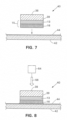
FIG. 7 , which is not covered by the claims, themultilayer solder article 24 can be formed into solder clad electrical devices of various configurations, including anelectrical connector 40, such as by stamping processes, by feeding theroll 24a into the appropriate processing machinery. Theelectrical connector 40 can include aconnector portion 38 which is formed from thebase substrate 11 into a desired configuration, for example, to engage a mating connector. Themultilayer solder 15 can be located on theelectrical connector 40 in a location suitable for solderingelectrical connector 40 to a surface, such as on abase 39. The layer of the first or highermelting temperature solder 13 can be sandwiched between the base 39 of theconnector portion 38 and the layer of the second or lowermelting temperature solder 16. - For examples of the
electrical connector 40 that are suitable for soldering toautomotive glass 42, thefirst solder 13 can have a composition that is suitable for bonding to the material ofconnector portion 38, for example, copper, and thesecond solder 16 can have a composition that is suitable for bonding to aterminal pad 44 on the surface ofautomotive glass 42. The first or highermelting temperature solder 13, not according to the present invention, can be a tin (Sn) and silver (Ag) solder, for example, having about 70% or greater tin, by weight. For example, in one example,solder 13 can be a tin and silver, solder having a composition of about 95% tin and about 5% silver, by weight (95Sn 5Ag). In other examples,solder 13 can have a variety of different amounts of tin, such as about 97% Sn 3% Ag, 90% Sn 10% Ag, 80% Sn 20% Ag, etc. In addition, some of the silver can be replaced by other elements. Although thefirst solder 13 is suitable for being bonded to theconnector portion 38, thefirst solder 13 might not be suitable for soldering to theautomotive glass 42, and might cause cracking of theglass 42. It has been observed by the Applicant that high tin solders typically cause cracking of automotive glass. - On the other hand, the second or lower
melting temperature solder 16, not according to the present invention, can have a lower tin (Sn) content and high indium (hi) content to allow soldering toautomotive glass 42 without cracking theglass 42. Thesecond solder 16 can be positioned on thebase 39 ofconnector portion 38 to contact theautomotive glass 42 and also to prevent contact of thefirst solder 13 with theglass 42. Thesecond solder 16 can have an indium (hi), tin (Sn), silver (Ag) and copper (Cu) composition with at least about 40% indium, less than about 55% tin, and the balance being about 3% to 5% silver and .25% to .75% copper, by weight. Some examples ofsolder 16 can have at least about 50% indium and about 45% or less tin. For example,solder 16 can have a composition of more than 50% indium, a maximum of about 30% tin, about 3% to 5% silver and about .25% to .75% copper. In one example,solder 16 can be about 65% indium, about 30% tin, about 4.5% silver and about .5% copper, by weight. The indium content can even be higher than 65%, thereby further reducing the percentage of tin. An example of a suitable solder composition forsolder 16 is disclosed inU.S. Patent No. 6,253,988, issued July 3, 2001 . The multilayer solder article can be formed with the desired solder compositions, and then, if desired, formed into electrical devices orelectrical connectors 40.Solder 13 andsolder 16 can both include silver to prevent or reduce the scavenging of silver from theautomobile glass 42. - Referring to
FIGs.7 and 8 , which are not covered by the claims, when solderingelectrical device 40 toautomotive glass 42, asoldering device 54 can apply a selected or programmed amount ofheat 56 for soldering theelectrical device 40 to theterminal pad 44 of theautomotive glass 42. Thesoldering device 54 can be microprocessor controlled and the amount of required heat can be preselected or preprogrammed, for example in watt/sec. Such a soldering device is commercially available from Antaya Technologies Corporation, in Cranston, Rhode Island. The programmed amount ofheat 56 can melt the second or lowermelting temperature solder 16 for soldering theelectrical device 40 to theglass 42 without substantially melting the first or highermelting temperature solder 13. Preferably, the first or highermelting temperature solder 13 does not melt at all, but slight melting is permitted, as long as there is not too much mixing of the two layers ofsolder glass 42 increases too much by the migration of tin from the layer of thefirst solder 13 into the layer of thesecond solder 16, cracking of theglass 42 can occur. - In one example, the
multilayer solder article 24 and resulting electrical device orelectrical connector 40 can have afirst solder 13 having a composition of 95Sn 5Ag, and asecond solder 16 having a composition of 65In 30Sn 4.5Ag .5Cu. The melting point or melting temperature (liquidus) of a 95Sn 5Agfirst solder 13 is about 465° F (241° C), and the solidus is about 430° F (221° C). The melting point or melting temperature (liquidus) of a 65In 30Sn 4.5Ag .5Cusecond solder 16 is about 250° F (121° C), and the solidus is about 245° F (118° C). As can be seen, the difference in melting temperatures between the 95Sn 5Agfirst solder 13 and the 65In 30Sn 4.5Ag .5Cusecond solder 16 can be about 215° F (102° C). Such a differential between the two melting temperatures can permit thesecond solder 16 to be melted without substantially melting thefirst solder 13. Whensolder 13 has a composition of 95Sn 5Ag andsolder 16 has a composition of 65In 30Sn 4.5Ag .5Cu, about 500 to 650 watt/sec ofheat 56 can be a suitable range for melting thesecond solder 16 but not thefirst solder 13. The amount of heat that is applied can differ depending upon the size and thickness of theconnector portion 38 and the volume ofsolder 16. In other examples, about 650 to 750 watt/sec can be suitable. - By having the
second solder 16 with a melting temperature below about 310° F (154° C), for example about 250° F (121° C), soldering thesecond solder 16 to theautomotive glass 42 at such a low temperature can minimize thermal stress on theautomotive glass 42. In addition, the extent of cooling that thesecond solder 16 experiences while cooling from the melting temperature to room temperature (for example down to about 70° F (21° C)) can be as little as a 180° F (82° C) temperature drop. Therefore, the amount of thermal shrinkage experienced by thesecond solder 16 can be kept to a minimum due to the small temperature drop, thereby minimizing the shrinkage differential between thesecond solder 16 and theautomotive glass 42.Automotive glass 42 has a very low coefficient thermal expansion relative to solder 16, and does not shrink as much assolder 16 during cooling. Furthermore, by including a high indium content, thesolder 16 can be ductile or soft enough to absorb thermal expansion differences between thesolder 16 and theautomotive glass 42 without cracking theglass 42. One or more of these factors can allow thesecond solder 16 to solder toautomotive glass 42 without cracking theglass 42. - In other examples, the melting temperatures of the first 13 and second 16 solders can vary depending upon the situation at hand and the compositions chosen. The melting temperature of the
first solder 13 can be lower than 465° F (241° C), for example, about 350° F (177° C), or can be higher, for example, above 500° F (260° C), and even as high as about 650° F (343° C). The melting temperature of the second solder can be below 250° F (121° C), for example, as low as 135° F (57° C), or can be higher than 310° F (154° C), for example 500° F (260° C) to 550° F (288° C). The compositions chosen for the first 13 and second 16 solders should have at least about a 100° F (38° C) difference in melting temperature to more easily enable the melting of thesecond solder 16 without substantially melting thefirst solder 13. It may be possible to have smaller differences in melting temperature depending upon the precision at which theheat 56 can be delivered and the compositions employed. - It has been found through further testing that additional examples of the
second solder 16 can have a greater range of tin and indium and be compatible or suitable for soldering on automotive glass without cracking or spalling the glass. Additional examples of thesecond solder 16 can have a composition with 55% or more tin (Sn) and 40% or less indium (In). The composition of thesecond solder 16 can have less than 90% tin (Sn) and greater than 10% indium (In), which in comparison to a high tin solder such as 95 Sn 5 Ag, is lower tin and high indium. The balance can be about 1% to 10% silver (Ag) (often about 1% to 6%), and about .25% to .75% copper (Cu). Examples of thesecond solder 16 can have a melting temperature at about 360° F (182° C) and below, and often about 320° F (160° C) and below. In some examples, the melting temperature can be below about 315° F (157° C) and in other examples, can be below about 310° F (154° C). - In one example, the
second solder 16 can be about 60% tin (Sn), about 35% indium (In), about 4.5% silver (Ag) and about .5% copper (Cu). The exact percentages can vary slightly due to normal variations in manufacturing, for example, about 59% to 61% Sn, about 34% to 36% In, about 4% to 5% Ag and about .4% to .6% Cu. The melting point or melting temperature (liquidus) can be about 300° F (149° C) and the solidus can be about 235° F (113° C). In another example, thesecond solder 16 can be about 50% Sn, about 46% hi, about 3.5% Ag and about .5% Cu. The exact percentages can vary slightly due to normal variations in manufacturing, for example, about 49% to 52% Sn, about 45% to 47% In, about 3% to 4% Ag and about .4% to .6% Cu. The melting point or melting temperature (liquidus) can be about 240° F (116° C) and the solidus can be about 235° F (113° C). These compositions of thesecond solder 16 can be used with afirst solder 13 having 95 Sn 5 Ag, as well as other suitable compositions, including those previously described. - A common composition range of the additional examples of the
second solder 16 can be at least about 50% tin, at least about 10% indium, 1% to 10% silver (often about 2% to 6%), and about .25% to .75% copper, in some situations, it is understood that further elements can also be included in thesecond solder 16 composition in addition to the tin, indium, silver and copper, typically, a relatively small percentage in comparison to the tin and indium. - The present invention provides another non-lead solder composition that is suitable for soldering electrical components to automotive glass for electrically connecting to electrical devices within or on the glass, as well as suitable for use as the
second solder 16 of a multilayer solder. Referring toFIG. 9 , the rearautomotive glass window 60 of an automobile is employed as an illustrative example for soldering electrical components to automotive glass.Automotive glass window 60 can include awindow defroster 62 consisting of electricallyresistive defrosting lines 64 embedded within or deposited on the inner surface ofwindow 60. The defrosting lines 64 can be electrically connected to a pair ofelectrical contacts 66 located on the inner surface of theglass 60. Theelectrical contacts 66 can consist of a conductive coating deposited on the inner surface of theglass 60. Often,electrical contacts 66 are formed from silver. - Referring to
FIG. 10 , thesolder composition 70, according to the present invention, is employed to solder anelectrical connector 72 to eachelectrical contact 66 on theglass 60.Power lines 74 can then be electrically connected toelectrical connectors 72 to provide power to window defroster 62 (FIG. 9 ). Soldering of theelectrical connectors 72 to theelectrical contacts 66 onglass 60 withsolder composition 70 can be conducted by resistance soldering. Alternatively, any conventional soldering apparatus can be employed to meltsolder composition 70, for example, a soldering iron. -
Solder composition 70 consists of tin (Sn), indium (In), silver (Ag)s and bismuth (Bi).Solder composition 70 can have a lower amount of tin than found in common high tin solder compositions. This can help prevent cracking and/or spalling ofautomotive glass 60 during soldering. Sufficient indium providessolder composition 70 with a relatively low melting point or temperature (liquidus) as well as mechanical properties which can prevent cracking and/or spalling ofautomotive glass 60. - Although too much bismuth can make
solder composition 70 brittle, the proper amount of bismuth in combination with the other elements providessolder composition 70 with a sufficiently low solidus temperature that also can help prevent cracking and/or spalling ofautomotive glass 60, without makingsolder composition 70 too brittle. The bismuth can provide a paste range between the liquidus and solidus temperatures which can be as small as about 30° F (17° C) and as large as about 140° F (78° C). A proper amount of bismuth keeps the solidus temperature below about 330° F (166° C), commonly below about 315° F (157° C). Some embodiments of thesolder composition 70 can have a solidus temperature of about 310° F (154° C) and less, for example, about 305° F (152° C) and less. The silver insolder composition 70 preventssolder composition 70 from scavenging silver from theelectrical contact 66 into thesolder composition 70. Finally, copper (Cu) is included withinsolder composition 70 for improving wetting. - By providing the
solder composition 70 with a relatively low melting temperature, thermal stress on theautomotive glass 60 is minimized. In addition, by providing the solder composition with a relatively low solidus temperature, the extent of cooling that thesolder composition 70 experiences while cooling from the solidus temperature to room temperature is minimized. Therefore, the amount of thermal shrinkage experienced by thesolder composition 70 after solidification is kept to a minimum due to a relatively small temperature drop, thereby minimizing the shrinkage differential and stresses between thesolder composition 70 and theautomotive glass 60. As previously mentioned, by including sufficient indium content, thesolder composition 70 is ductile or soft enough to absorb thermal expansion differences between thesolder composition 70 and theautomotive glass 60 without cracking and/or spalling theglass 60. - The compositional range for
solder composition 70 consists of 50% to 83% tin, 13% to 45% indium (often 15% to 45%), 1% to 10% silver, and .25% to 6% bismuth, by weight. Additional embodiments includes 66% to 83% tin, and 13% to 26% indium (often 15% to 26%). Particular embodiments can include 70% to 80% tin, and 15% to 26% indium. The embodiments include .25% to .75% copper. In some embodiments there can be 1% to 6% silver, .25% to 4% bismuth and .25% to .75% copper. - To make
solder composition 70, ingots of indium, tin, silver, bismuth and copper are melted and mixed together. Alternatively, the elements can be melted from powder form or a desired combination of ingots, powder and/or existing solder compositions. Themixed solder composition 70 can then be cast, extruded or rolled into a shape suitable for soldering, for example, a ribbon, wire, etc. If desired, thesolder composition 70 can be formed into a paste. - In one embodiment,
solder composition 70 can consists of 51% tin, 42% indium, 3.5% silver, 3% bismuth and .5% copper. The melting point or temperature (liquidus) can be about 253° F (123° C) and the solidus can be about 223° F (106° C), resulting in a paste range of about 30° F (17° C). - In another embodiment, the
solder composition 70 consists of 60% to 63% tin, 28% to 33% indium, 1% to 6% silver, .25% to 4% bismuth, and .25% to .75% copper. For example,solder composition 70 consists of 62% tin, 30% indium, 5% silver, 2.5% bismuth, and .5% copper. The melting point or temperature (liquidus) can be about 311° F (155° C) and the solidus can be about 226° F (108° C), resulting in a paste range of about 85° F (47° C). In another example, thesolder composition 70 consists of 62% tin, 32% indium, 4.5% silver, 1% bismuth and .5% copper. The melting point or temperature (liquidus) can be about 336° F (169° C) and the solidus can be about 199° F (93° C), resulting in a paste range of about 137° F (76° C). The coefficient of thermal expansion (CTE) can be about 10×10-6/F (19.7×10⁻⁶/° C). - In still another embodiment, the
solder composition 70 consists of 68% tin, 24% indium, 6% silver, 1.5% bismuth and .5% copper. The actual percentages can vary slightly, for example, 66% to 69% tin, 22% to 26% indium, 1% to 7% silver, .25% to 4% bismuth, and .25% to .75% copper. The melting point or temperature (liquidus) can be about 360° F (182° C) and the solidus can be about 235° F (113° C), resulting in a paste range of about 125° F (69° C). The coefficient of thermal expansion (CTE) can be about 10.910-6/ F (19.6×10⁻⁶/° C). - In another embodiment, the
solder composition 70 consists of 70% to 74% tin, 18% to 26% indium, 1% to 6% silver, .25% to 4% bismuth, and .25% to .75% copper. For example, thesolder composition 70 consists of 72% tin, 19% indium, 5% silver, 3.5% bismuth and .5% copper. The melting point or temperature (liquidus) can be about 370° F (188° C) and the solidus can be about 273° F (134° C), resulting in a paste range of about 97° F (54° C). The coefficient of thermal expansion (CTE) can be about 10.8×10⁻⁶/° F (19.5×10⁻⁶/° C). In another example, thesolder composition 70 consists of 72% tin, 24% indium, 2% silver, 1.5 % bismuth and .5% copper. The melting point or temperature (liquidus) can be in the range of about 379° F (193° C) to 385° F (196° C) with an average of about 382° F (194° C), and the solidus can be in the range of about 221° F (105° C) to 233° F (112° C) with an average of about 227° F (108° C). This can result in an average paste range of about 155° F (86° C). The coefficient of thermal expansion (CTE) can have an average of about 12.5×10⁻⁶/° F (22.5×10⁻⁶/ C). - In another embodiment, the
solder composition 70 consists of 73% to 78% tin, 17% to 22% indium, 1% to 6% silver, .25% to 4% bismuth, and .25% to .75% copper. For example,solder composition 70 consists of 75% tin, 19% indium, 3.5% silver, 2% bismuth and .5% copper. The melting point or temperature (liquidus) can be about 381° F (194° C) and the solidus can be about 284° F (140° C), resulting in a paste range of about 97° F (54° C). The coefficient of thermal expansion (CTE) can be about 10×10-6/0 F (18×l0-6/° C) and the density can be about 7.4 g/cm3. In another example, the solder composition consists of 75% tin, 20.5% indium, 2.5% silver, 1.5% bismuth and .5% copper. The melting point or temperature (liquidus) can be about 372° F (189°C) and the solidus can be about 278°F (137°C), resulting in a paste range of about 94° F (52° C). In another example, thesolder composition 70 can include about 77% tin, about 18% indium, about 3% silver, about 1.5% bismuth and about .5% copper. The melting point or temperature (liquidus) can be about 379° F (193°C) and the solidus can be about 297° F (147°C), resulting in a paste range of about 82° F (46° C). The coefficient of thermal expansion (CTE) can be about 8.8×l0-6/ F (15.9×l0-6/ C). - For example,
solder composition 70 consists of 80% tin, 15% indium, 3.5% silver, about 1% bismuth and .5% copper. The melting point or temperature (liquidus) can be about 390° F (199° C) and the solidus can be about 304°F (151°C), resulting in a paste range of about 86° F (48° C). The coefficient of thermal expansion (CTE) can be about 8.5×10⁻⁶/ F (15.3×10-δ/°C). In another example, thesolder composition 70 consists of 83% tin, 13% indium, 2.5% silver, 1% bismuth, and .5% copper. The melting point or temperature (liquidus) can be about 399° F (204°C) and the solidus can be about 305° F (152°C), resulting in a paste range of about 94° F (52° C). The coefficient of thermal expansion (CTE) can be about
7.6×10⁻⁶/°F (13.7×10⁻⁶/°C). For example, theapparatus 10 can be employed for bonding more than two layers of solder together, resulting in a multilayer solder article, electrical device or electrical connector having more than two layers of solder. In addition, the mating surfaces of thesolders 13/16 can be pretreated for bonding purposes. In embodiments where the multilayer solder article does not have abase substrate 11 , the multilayer solder article can be subsequently bonded or positioned relative to products requiring soldering. A rolling process can also be used to bond thefirst solder 13 to thebase substrate 11. Althoughmultilayer solder article 24 has been shown and described to be formed employing cold rolling processes, alternatively,article 24 and/or electrical device orconnector 40 can be formed employing other processes, for example, deposition or reflow processes. Ultrasonic or resistance welding devices can also be employed for bonding desired layers of material together. For example, the solders can be applied to thebase substrate 11 by welding processes.
Claims (12)
- A solder composition, consisting of50% to 83% tin;13% to 45% indium;1 to 10% silver;0.25% to 6% bismuth; and0.25% to 0.75% copper,wherein the solder composition has a solidus temperature below 157°C.
- The solder composition according to claim 1, wherein the solder composition includes 1 to 6% silver.
- The solder composition according to any one of the preceding claims, wherein the solder composition includes 0.25% to 4% bismuth.
- The solder composition according to any one of the preceding claims, wherein the solder composition includes 15% to 45% indium.
- The solder composition according to any one of the preceding claims, wherein the solder composition includes 66% to 83% tin and 13% to 26% indium.
- The solder composition according to any one of the preceding claims, wherein the solder composition includes 70% to 80% tin and 15% to 26% indium.
- The solder composition according to any one of the preceding claims, wherein the solder composition includes 73% to 78% tin and 17% to 22% indium.
- The solder composition according to any one of the preceding claims, wherein the solder composition consists of 66% to 83% tin and 15% to 26% indium, 1 to 6% silver, 0.25% to 4% bismuth, and 0.25% to 0.75% copper.
- The solder composition according to any one of the preceding claims, wherein the solder composition consists of 70% to 74% tin and 18% to 26% indium, 1% to 6% silver, 0.25% to 4% bismuth, and 0.25% to 0.75% copper.
- The solder composition according to any one of the preceding claims, wherein the solder composition consists of 73% to 78% tin and 17% to 22% indium, 1% to 6% silver, 0.25% to 4% bismuth, and 0.25% to 0.75% copper.
- The solder composition according to any one of the preceding claims, wherein the solder composition consists of 60% to 63% tin and 28% to 33% indium, 1% to 6% silver, 0.25% to 4% bismuth, and 0.25% to 0.75% copper.
- The solder composition according to any one of the preceding claims, wherein the solder composition consists of 66% to 69% tin and 22% to 36% indium, 1% to 7% silver, 0.25% to 4% bismuth, and 0.25% to 0.75% copper.
Applications Claiming Priority (5)
| Application Number | Priority Date | Filing Date | Title |
|---|---|---|---|
| US11/202,640 US20070037004A1 (en) | 2005-08-12 | 2005-08-12 | Multilayer solder article |
| US11/359,864 US20070036670A1 (en) | 2005-08-12 | 2006-02-22 | Solder composition |
| US11/359,876 US20070231594A1 (en) | 2005-08-12 | 2006-02-22 | Multilayer solder article |
| EP06750366.4A EP1922175B1 (en) | 2005-08-12 | 2006-04-12 | Solder composition |
| PCT/US2006/014305 WO2007021326A2 (en) | 2005-08-12 | 2006-04-13 | Solder composition |
Related Parent Applications (1)
| Application Number | Title | Priority Date | Filing Date |
|---|---|---|---|
| EP06750366.4A Division EP1922175B1 (en) | 2005-08-12 | 2006-04-12 | Solder composition |
Publications (2)
| Publication Number | Publication Date |
|---|---|
| EP3590653A1 EP3590653A1 (en) | 2020-01-08 |
| EP3590653B1 true EP3590653B1 (en) | 2023-10-18 |
Family
ID=36951374
Family Applications (2)
| Application Number | Title | Priority Date | Filing Date |
|---|---|---|---|
| EP19193508.9A Active EP3590653B1 (en) | 2005-08-12 | 2006-04-12 | Solder composition |
| EP06750366.4A Active EP1922175B1 (en) | 2005-08-12 | 2006-04-12 | Solder composition |
Family Applications After (1)
| Application Number | Title | Priority Date | Filing Date |
|---|---|---|---|
| EP06750366.4A Active EP1922175B1 (en) | 2005-08-12 | 2006-04-12 | Solder composition |
Country Status (5)
| Country | Link |
|---|---|
| EP (2) | EP3590653B1 (en) |
| JP (1) | JP5492412B2 (en) |
| CA (1) | CA2625021A1 (en) |
| PL (1) | PL1922175T3 (en) |
| WO (1) | WO2007021326A2 (en) |
Families Citing this family (17)
| Publication number | Priority date | Publication date | Assignee | Title |
|---|---|---|---|---|
| JP5696173B2 (en) * | 2005-08-12 | 2015-04-08 | アンタヤ・テクノロジーズ・コープ | Solder composition |
| JP2009269075A (en) * | 2008-05-09 | 2009-11-19 | Sumitomo Metal Mining Co Ltd | Method and apparatus for manufacturing stacked solder material having stress relaxation layer |
| DE102009034483A1 (en) * | 2009-07-22 | 2011-01-27 | W.C. Heraeus Gmbh | Lead-free high-temperature connection for the AVT in electronics |
| JP2011240352A (en) * | 2010-05-17 | 2011-12-01 | Central Glass Co Ltd | Lead-free solder composition for vehicle |
| EP2664503B1 (en) | 2011-01-14 | 2018-03-07 | Asahi Glass Company, Limited | A method for producing a windowpane for vehicles |
| EP2670560B1 (en) * | 2011-02-04 | 2016-01-13 | Antaya Technologies Corp. | Lead-free solder composition |
| KR101545798B1 (en) | 2011-03-02 | 2015-08-19 | 샌트랄 글래스 컴퍼니 리미티드 | Lead-free solder alloy for vehicle glass |
| JP2014096198A (en) * | 2011-03-02 | 2014-05-22 | Central Glass Co Ltd | Method of bonding window pane for automobiles and feeding terminal |
| US9595768B2 (en) | 2011-05-03 | 2017-03-14 | Pilkington Group Limited | Glazing with a soldered connector |
| GB201114076D0 (en) | 2011-08-16 | 2011-09-28 | Pilkington Group Ltd | Glazing |
| CN104540636B (en) * | 2012-08-24 | 2017-09-08 | 法国圣戈班玻璃厂 | Glass plate with electrical connecting element |
| CN203936494U (en) * | 2014-02-28 | 2014-11-12 | 日本斯倍利亚社股份有限公司 | Automotive glass |
| KR101555779B1 (en) * | 2014-04-11 | 2015-09-24 | (주)한신단자공업 | Power clip for windshield manufacturing method |
| KR101555778B1 (en) * | 2014-04-11 | 2015-09-24 | (주)한신단자공업 | Power clip for windshield manufacturing method and Power clip for windshield |
| KR20170108766A (en) * | 2016-03-18 | 2017-09-27 | 헤베이 리신 테크놀로지 컴퍼니 리미티드 | Lead free solder composition with high ductility |
| EP3898070A1 (en) * | 2018-12-17 | 2021-10-27 | Heraeus Precious Metals North America Conshohocken LLC | Process for forming an electric heater |
| US11383330B2 (en) | 2020-09-21 | 2022-07-12 | Aptiv Technologies Limited | Lead-free solder composition |
Family Cites Families (5)
| Publication number | Priority date | Publication date | Assignee | Title |
|---|---|---|---|---|
| JPH0680881B2 (en) * | 1984-06-29 | 1994-10-12 | 富士通株式会社 | Solder melting type high density connector |
| JPH03230552A (en) * | 1990-02-05 | 1991-10-14 | Matsushita Electric Ind Co Ltd | Joint material for packaging semiconductor device |
| JP2000141078A (en) * | 1998-09-08 | 2000-05-23 | Nippon Sheet Glass Co Ltd | Leadless solder |
| US6253988B1 (en) | 1999-03-29 | 2001-07-03 | Antaya Technologies Corporation | Low temperature solder |
| JP2002096191A (en) * | 2000-09-18 | 2002-04-02 | Matsushita Electric Ind Co Ltd | Soldering material and electric/electronic equipment using the same |
-
2006
- 2006-04-12 PL PL06750366T patent/PL1922175T3/en unknown
- 2006-04-12 EP EP19193508.9A patent/EP3590653B1/en active Active
- 2006-04-12 EP EP06750366.4A patent/EP1922175B1/en active Active
- 2006-04-13 WO PCT/US2006/014305 patent/WO2007021326A2/en active Application Filing
- 2006-04-13 JP JP2008525984A patent/JP5492412B2/en active Active
- 2006-04-13 CA CA002625021A patent/CA2625021A1/en not_active Abandoned
Also Published As
| Publication number | Publication date |
|---|---|
| EP1922175A2 (en) | 2008-05-21 |
| EP3590653A1 (en) | 2020-01-08 |
| PL1922175T3 (en) | 2020-03-31 |
| CA2625021A1 (en) | 2007-02-22 |
| EP1922175B1 (en) | 2019-09-04 |
| JP5492412B2 (en) | 2014-05-14 |
| JP2009504411A (en) | 2009-02-05 |
| WO2007021326A2 (en) | 2007-02-22 |
| WO2007021326A3 (en) | 2007-06-21 |
Similar Documents
| Publication | Publication Date | Title |
|---|---|---|
| EP3590653B1 (en) | Solder composition | |
| US20070231594A1 (en) | Multilayer solder article | |
| US20080175748A1 (en) | Solder Composition | |
| US20070036670A1 (en) | Solder composition | |
| US20070037004A1 (en) | Multilayer solder article | |
| US20070292708A1 (en) | Solder composition | |
| US7972710B2 (en) | Clad aluminum connector | |
| JP6087404B2 (en) | Electrical device with multiple solder layers | |
| EP1758175B2 (en) | Electrode wire for solar battery | |
| EP1626443B1 (en) | Electrode wire material and solar battery having connection lead formed of the wire material | |
| EP1488972B2 (en) | Metal fixture-joined glass article, and joint structure using this | |
| EP0617833B1 (en) | Process for pre-soldering a contact base for an electric circuit component and semi-finished product for use as a contact base | |
| US3568301A (en) | Bonding of precious metal to a metal substrate and product therefor | |
| EP2055425A1 (en) | Process for producing cladding material and cladding material | |
| JP2013132689A (en) | Aluminum brazing sheet, brazed structure using the same, and method for manufacturing the aluminum brazing sheet | |
| MX2008001874A (en) | Solder composition | |
| US20030096135A1 (en) | Composite jewelry metal | |
| JPH05329681A (en) | Multilayered brazing filler metal and its production and connecting method | |
| JPS6120116B2 (en) | ||
| US20230303433A1 (en) | Method of attaching a connector to a glazing | |
| CN108788510B (en) | Lead-free solder alloy, preparation method and application thereof, and glass assembly | |
| EP0385785A1 (en) | Production of heated windows | |
| JP4600299B2 (en) | Method for producing solder clad material | |
| JP2013132687A (en) | Aluminum brazing sheet, brazed structure using the same, and method for manufacturing the aluminum brazing sheet | |
| JPH02103815A (en) | Manufacture of partially solder clad plate |
Legal Events
| Date | Code | Title | Description |
|---|---|---|---|
| PUAI | Public reference made under article 153(3) epc to a published international application that has entered the european phase |
Free format text: ORIGINAL CODE: 0009012 |
|
| STAA | Information on the status of an ep patent application or granted ep patent |
Free format text: STATUS: THE APPLICATION HAS BEEN PUBLISHED |
|
| AC | Divisional application: reference to earlier application |
Ref document number: 1922175 Country of ref document: EP Kind code of ref document: P |
|
| AK | Designated contracting states |
Kind code of ref document: A1 Designated state(s): AT BE BG CH CY CZ DE DK EE ES FI FR GB GR HU IE IS IT LI LT LU LV MC NL PL PT RO SE SI SK TR |
|
| STAA | Information on the status of an ep patent application or granted ep patent |
Free format text: STATUS: REQUEST FOR EXAMINATION WAS MADE |
|
| 17P | Request for examination filed |
Effective date: 20200703 |
|
| RBV | Designated contracting states (corrected) |
Designated state(s): AT BE BG CH CY CZ DE DK EE ES FI FR GB GR HU IE IS IT LI LT LU LV MC NL PL PT RO SE SI SK TR |
|
| STAA | Information on the status of an ep patent application or granted ep patent |
Free format text: STATUS: EXAMINATION IS IN PROGRESS |
|
| 17Q | First examination report despatched |
Effective date: 20201201 |
|
| STAA | Information on the status of an ep patent application or granted ep patent |
Free format text: STATUS: EXAMINATION IS IN PROGRESS |
|
| RIC1 | Information provided on ipc code assigned before grant |
Ipc: B23K 35/26 20060101AFI20210621BHEP Ipc: B23K 35/30 20060101ALI20210621BHEP Ipc: C03C 17/36 20060101ALI20210621BHEP Ipc: C03C 27/04 20060101ALI20210621BHEP Ipc: B32B 15/01 20060101ALI20210621BHEP Ipc: B23K 35/02 20060101ALI20210621BHEP Ipc: C22C 13/00 20060101ALI20210621BHEP Ipc: C22C 30/04 20060101ALI20210621BHEP Ipc: C22C 28/00 20060101ALI20210621BHEP |
|
| RAP3 | Party data changed (applicant data changed or rights of an application transferred) |
Owner name: APTIV TECHNOLOGIES LIMITED |
|
| GRAP | Despatch of communication of intention to grant a patent |
Free format text: ORIGINAL CODE: EPIDOSNIGR1 |
|
| STAA | Information on the status of an ep patent application or granted ep patent |
Free format text: STATUS: GRANT OF PATENT IS INTENDED |
|
| INTG | Intention to grant announced |
Effective date: 20230810 |
|
| GRAS | Grant fee paid |
Free format text: ORIGINAL CODE: EPIDOSNIGR3 |
|
| GRAA | (expected) grant |
Free format text: ORIGINAL CODE: 0009210 |
|
| STAA | Information on the status of an ep patent application or granted ep patent |
Free format text: STATUS: THE PATENT HAS BEEN GRANTED |
|
| AC | Divisional application: reference to earlier application |
Ref document number: 1922175 Country of ref document: EP Kind code of ref document: P |
|
| AK | Designated contracting states |
Kind code of ref document: B1 Designated state(s): AT BE BG CH CY CZ DE DK EE ES FI FR GB GR HU IE IS IT LI LT LU LV MC NL PL PT RO SE SI SK TR |
|
| P01 | Opt-out of the competence of the unified patent court (upc) registered |
Effective date: 20230908 |
|
| REG | Reference to a national code |
Ref country code: GB Ref legal event code: FG4D |
|
| REG | Reference to a national code |
Ref country code: CH Ref legal event code: EP |
|
| REG | Reference to a national code |
Ref country code: DE Ref legal event code: R096 Ref document number: 602006060508 Country of ref document: DE |
|
| REG | Reference to a national code |
Ref country code: IE Ref legal event code: FG4D |
|
| REG | Reference to a national code |
Ref country code: LT Ref legal event code: MG9D |
|
| REG | Reference to a national code |
Ref country code: NL Ref legal event code: MP Effective date: 20231018 |
|
| REG | Reference to a national code |
Ref country code: AT Ref legal event code: MK05 Ref document number: 1621991 Country of ref document: AT Kind code of ref document: T Effective date: 20231018 |
|
| PG25 | Lapsed in a contracting state [announced via postgrant information from national office to epo] |
Ref country code: NL Free format text: LAPSE BECAUSE OF FAILURE TO SUBMIT A TRANSLATION OF THE DESCRIPTION OR TO PAY THE FEE WITHIN THE PRESCRIBED TIME-LIMIT Effective date: 20231018 |
|
| PG25 | Lapsed in a contracting state [announced via postgrant information from national office to epo] |
Ref country code: GR Free format text: LAPSE BECAUSE OF FAILURE TO SUBMIT A TRANSLATION OF THE DESCRIPTION OR TO PAY THE FEE WITHIN THE PRESCRIBED TIME-LIMIT Effective date: 20240119 |
|
| PG25 | Lapsed in a contracting state [announced via postgrant information from national office to epo] |
Ref country code: IS Free format text: LAPSE BECAUSE OF FAILURE TO SUBMIT A TRANSLATION OF THE DESCRIPTION OR TO PAY THE FEE WITHIN THE PRESCRIBED TIME-LIMIT Effective date: 20240218 |
|
| PG25 | Lapsed in a contracting state [announced via postgrant information from national office to epo] |
Ref country code: LT Free format text: LAPSE BECAUSE OF FAILURE TO SUBMIT A TRANSLATION OF THE DESCRIPTION OR TO PAY THE FEE WITHIN THE PRESCRIBED TIME-LIMIT Effective date: 20231018 |