EP2887415B1 - Oled-beleuchtungsmodul - Google Patents
Oled-beleuchtungsmodul Download PDFInfo
- Publication number
- EP2887415B1 EP2887415B1 EP13836856.8A EP13836856A EP2887415B1 EP 2887415 B1 EP2887415 B1 EP 2887415B1 EP 13836856 A EP13836856 A EP 13836856A EP 2887415 B1 EP2887415 B1 EP 2887415B1
- Authority
- EP
- European Patent Office
- Prior art keywords
- oled
- lighting module
- transparent electrode
- connection terminal
- substrate portion
- Prior art date
- Legal status (The legal status is an assumption and is not a legal conclusion. Google has not performed a legal analysis and makes no representation as to the accuracy of the status listed.)
- Active
Links
Images




Classifications
-
- H—ELECTRICITY
- H05—ELECTRIC TECHNIQUES NOT OTHERWISE PROVIDED FOR
- H05K—PRINTED CIRCUITS; CASINGS OR CONSTRUCTIONAL DETAILS OF ELECTRIC APPARATUS; MANUFACTURE OF ASSEMBLAGES OF ELECTRICAL COMPONENTS
- H05K1/00—Printed circuits
- H05K1/18—Printed circuits structurally associated with non-printed electric components
- H05K1/189—Printed circuits structurally associated with non-printed electric components characterised by the use of flexible or folded printed circuits
-
- F—MECHANICAL ENGINEERING; LIGHTING; HEATING; WEAPONS; BLASTING
- F21—LIGHTING
- F21K—NON-ELECTRIC LIGHT SOURCES USING LUMINESCENCE; LIGHT SOURCES USING ELECTROCHEMILUMINESCENCE; LIGHT SOURCES USING CHARGES OF COMBUSTIBLE MATERIAL; LIGHT SOURCES USING SEMICONDUCTOR DEVICES AS LIGHT-GENERATING ELEMENTS; LIGHT SOURCES NOT OTHERWISE PROVIDED FOR
- F21K9/00—Light sources using semiconductor devices as light-generating elements, e.g. using light-emitting diodes [LED] or lasers
- F21K9/20—Light sources comprising attachment means
-
- F—MECHANICAL ENGINEERING; LIGHTING; HEATING; WEAPONS; BLASTING
- F21—LIGHTING
- F21V—FUNCTIONAL FEATURES OR DETAILS OF LIGHTING DEVICES OR SYSTEMS THEREOF; STRUCTURAL COMBINATIONS OF LIGHTING DEVICES WITH OTHER ARTICLES, NOT OTHERWISE PROVIDED FOR
- F21V19/00—Fastening of light sources or lamp holders
- F21V19/001—Fastening of light sources or lamp holders the light sources being semiconductors devices, e.g. LEDs
- F21V19/0015—Fastening arrangements intended to retain light sources
- F21V19/0025—Fastening arrangements intended to retain light sources the fastening means engaging the conductors of the light source, i.e. providing simultaneous fastening of the light sources and their electric connections
-
- H—ELECTRICITY
- H05—ELECTRIC TECHNIQUES NOT OTHERWISE PROVIDED FOR
- H05B—ELECTRIC HEATING; ELECTRIC LIGHT SOURCES NOT OTHERWISE PROVIDED FOR; CIRCUIT ARRANGEMENTS FOR ELECTRIC LIGHT SOURCES, IN GENERAL
- H05B33/00—Electroluminescent light sources
- H05B33/02—Details
- H05B33/06—Electrode terminals
-
- H—ELECTRICITY
- H05—ELECTRIC TECHNIQUES NOT OTHERWISE PROVIDED FOR
- H05B—ELECTRIC HEATING; ELECTRIC LIGHT SOURCES NOT OTHERWISE PROVIDED FOR; CIRCUIT ARRANGEMENTS FOR ELECTRIC LIGHT SOURCES, IN GENERAL
- H05B33/00—Electroluminescent light sources
- H05B33/12—Light sources with substantially two-dimensional [2D] radiating surfaces
- H05B33/14—Light sources with substantially two-dimensional [2D] radiating surfaces characterised by the chemical or physical composition or the arrangement of the electroluminescent material, or by the simultaneous addition of the electroluminescent material in or onto the light source
- H05B33/145—Arrangements of the electroluminescent material
-
- H—ELECTRICITY
- H05—ELECTRIC TECHNIQUES NOT OTHERWISE PROVIDED FOR
- H05B—ELECTRIC HEATING; ELECTRIC LIGHT SOURCES NOT OTHERWISE PROVIDED FOR; CIRCUIT ARRANGEMENTS FOR ELECTRIC LIGHT SOURCES, IN GENERAL
- H05B33/00—Electroluminescent light sources
- H05B33/12—Light sources with substantially two-dimensional [2D] radiating surfaces
- H05B33/26—Light sources with substantially two-dimensional [2D] radiating surfaces characterised by the composition or arrangement of the conductive material used as an electrode
- H05B33/28—Light sources with substantially two-dimensional [2D] radiating surfaces characterised by the composition or arrangement of the conductive material used as an electrode of translucent electrodes
-
- H—ELECTRICITY
- H05—ELECTRIC TECHNIQUES NOT OTHERWISE PROVIDED FOR
- H05K—PRINTED CIRCUITS; CASINGS OR CONSTRUCTIONAL DETAILS OF ELECTRIC APPARATUS; MANUFACTURE OF ASSEMBLAGES OF ELECTRICAL COMPONENTS
- H05K3/00—Apparatus or processes for manufacturing printed circuits
- H05K3/40—Forming printed elements for providing electric connections to or between printed circuits
- H05K3/4007—Surface contacts, e.g. bumps
- H05K3/4015—Surface contacts, e.g. bumps using auxiliary conductive elements, e.g. pieces of metal foil, metallic spheres
-
- H—ELECTRICITY
- H10—SEMICONDUCTOR DEVICES; ELECTRIC SOLID-STATE DEVICES NOT OTHERWISE PROVIDED FOR
- H10K—ORGANIC ELECTRIC SOLID-STATE DEVICES
- H10K50/00—Organic light-emitting devices
-
- H—ELECTRICITY
- H10—SEMICONDUCTOR DEVICES; ELECTRIC SOLID-STATE DEVICES NOT OTHERWISE PROVIDED FOR
- H10W—GENERIC PACKAGES, INTERCONNECTIONS, CONNECTORS OR OTHER CONSTRUCTIONAL DETAILS OF DEVICES COVERED BY CLASS H10
- H10W20/00—Interconnections in chips, wafers or substrates
- H10W20/40—Interconnections external to wafers or substrates, e.g. back-end-of-line [BEOL] metallisations or vias connecting to gate electrodes
-
- H—ELECTRICITY
- H10—SEMICONDUCTOR DEVICES; ELECTRIC SOLID-STATE DEVICES NOT OTHERWISE PROVIDED FOR
- H10W—GENERIC PACKAGES, INTERCONNECTIONS, CONNECTORS OR OTHER CONSTRUCTIONAL DETAILS OF DEVICES COVERED BY CLASS H10
- H10W70/00—Package substrates; Interposers; Redistribution layers [RDL]
- H10W70/01—Manufacture or treatment
- H10W70/05—Manufacture or treatment of insulating or insulated package substrates, or of interposers, or of redistribution layers
- H10W70/098—Applying pastes or inks, e.g. screen printing
-
- F—MECHANICAL ENGINEERING; LIGHTING; HEATING; WEAPONS; BLASTING
- F21—LIGHTING
- F21Y—INDEXING SCHEME ASSOCIATED WITH SUBCLASSES F21K, F21L, F21S and F21V, RELATING TO THE FORM OR THE KIND OF THE LIGHT SOURCES OR OF THE COLOUR OF THE LIGHT EMITTED
- F21Y2105/00—Planar light sources
-
- F—MECHANICAL ENGINEERING; LIGHTING; HEATING; WEAPONS; BLASTING
- F21—LIGHTING
- F21Y—INDEXING SCHEME ASSOCIATED WITH SUBCLASSES F21K, F21L, F21S and F21V, RELATING TO THE FORM OR THE KIND OF THE LIGHT SOURCES OR OF THE COLOUR OF THE LIGHT EMITTED
- F21Y2105/00—Planar light sources
- F21Y2105/10—Planar light sources comprising a two-dimensional [2D] array of point-like light-generating elements
-
- F—MECHANICAL ENGINEERING; LIGHTING; HEATING; WEAPONS; BLASTING
- F21—LIGHTING
- F21Y—INDEXING SCHEME ASSOCIATED WITH SUBCLASSES F21K, F21L, F21S and F21V, RELATING TO THE FORM OR THE KIND OF THE LIGHT SOURCES OR OF THE COLOUR OF THE LIGHT EMITTED
- F21Y2115/00—Light-generating elements of semiconductor light sources
- F21Y2115/10—Light-emitting diodes [LED]
- F21Y2115/15—Organic light-emitting diodes [OLED]
-
- H—ELECTRICITY
- H05—ELECTRIC TECHNIQUES NOT OTHERWISE PROVIDED FOR
- H05K—PRINTED CIRCUITS; CASINGS OR CONSTRUCTIONAL DETAILS OF ELECTRIC APPARATUS; MANUFACTURE OF ASSEMBLAGES OF ELECTRICAL COMPONENTS
- H05K2201/00—Indexing scheme relating to printed circuits covered by H05K1/00
- H05K2201/05—Flexible printed circuits [FPCs]
- H05K2201/053—Tails
-
- H—ELECTRICITY
- H05—ELECTRIC TECHNIQUES NOT OTHERWISE PROVIDED FOR
- H05K—PRINTED CIRCUITS; CASINGS OR CONSTRUCTIONAL DETAILS OF ELECTRIC APPARATUS; MANUFACTURE OF ASSEMBLAGES OF ELECTRICAL COMPONENTS
- H05K2201/00—Indexing scheme relating to printed circuits covered by H05K1/00
- H05K2201/05—Flexible printed circuits [FPCs]
- H05K2201/056—Folded around rigid support or component
-
- H—ELECTRICITY
- H05—ELECTRIC TECHNIQUES NOT OTHERWISE PROVIDED FOR
- H05K—PRINTED CIRCUITS; CASINGS OR CONSTRUCTIONAL DETAILS OF ELECTRIC APPARATUS; MANUFACTURE OF ASSEMBLAGES OF ELECTRICAL COMPONENTS
- H05K2201/00—Indexing scheme relating to printed circuits covered by H05K1/00
- H05K2201/09—Shape and layout
- H05K2201/09818—Shape or layout details not covered by a single group of H05K2201/09009 - H05K2201/09809
- H05K2201/09845—Stepped hole, via, edge, bump or conductor
-
- H—ELECTRICITY
- H05—ELECTRIC TECHNIQUES NOT OTHERWISE PROVIDED FOR
- H05K—PRINTED CIRCUITS; CASINGS OR CONSTRUCTIONAL DETAILS OF ELECTRIC APPARATUS; MANUFACTURE OF ASSEMBLAGES OF ELECTRICAL COMPONENTS
- H05K2201/00—Indexing scheme relating to printed circuits covered by H05K1/00
- H05K2201/10—Details of components or other objects attached to or integrated in a printed circuit board
- H05K2201/10007—Types of components
- H05K2201/10128—Display
-
- H—ELECTRICITY
- H05—ELECTRIC TECHNIQUES NOT OTHERWISE PROVIDED FOR
- H05K—PRINTED CIRCUITS; CASINGS OR CONSTRUCTIONAL DETAILS OF ELECTRIC APPARATUS; MANUFACTURE OF ASSEMBLAGES OF ELECTRICAL COMPONENTS
- H05K2201/00—Indexing scheme relating to printed circuits covered by H05K1/00
- H05K2201/10—Details of components or other objects attached to or integrated in a printed circuit board
- H05K2201/10227—Other objects, e.g. metallic pieces
- H05K2201/1031—Surface mounted metallic connector elements
-
- H—ELECTRICITY
- H05—ELECTRIC TECHNIQUES NOT OTHERWISE PROVIDED FOR
- H05K—PRINTED CIRCUITS; CASINGS OR CONSTRUCTIONAL DETAILS OF ELECTRIC APPARATUS; MANUFACTURE OF ASSEMBLAGES OF ELECTRICAL COMPONENTS
- H05K2201/00—Indexing scheme relating to printed circuits covered by H05K1/00
- H05K2201/10—Details of components or other objects attached to or integrated in a printed circuit board
- H05K2201/10227—Other objects, e.g. metallic pieces
- H05K2201/1031—Surface mounted metallic connector elements
- H05K2201/10318—Surface mounted metallic pins
-
- H—ELECTRICITY
- H05—ELECTRIC TECHNIQUES NOT OTHERWISE PROVIDED FOR
- H05K—PRINTED CIRCUITS; CASINGS OR CONSTRUCTIONAL DETAILS OF ELECTRIC APPARATUS; MANUFACTURE OF ASSEMBLAGES OF ELECTRICAL COMPONENTS
- H05K3/00—Apparatus or processes for manufacturing printed circuits
- H05K3/30—Assembling printed circuits with electric components, e.g. with resistors
- H05K3/32—Assembling printed circuits with electric components, e.g. with resistors electrically connecting electric components or wires to printed circuits
- H05K3/321—Assembling printed circuits with electric components, e.g. with resistors electrically connecting electric components or wires to printed circuits by conductive adhesives
- H05K3/323—Assembling printed circuits with electric components, e.g. with resistors electrically connecting electric components or wires to printed circuits by conductive adhesives by applying an anisotropic conductive adhesive layer over an array of pads
-
- Y—GENERAL TAGGING OF NEW TECHNOLOGICAL DEVELOPMENTS; GENERAL TAGGING OF CROSS-SECTIONAL TECHNOLOGIES SPANNING OVER SEVERAL SECTIONS OF THE IPC; TECHNICAL SUBJECTS COVERED BY FORMER USPC CROSS-REFERENCE ART COLLECTIONS [XRACs] AND DIGESTS
- Y02—TECHNOLOGIES OR APPLICATIONS FOR MITIGATION OR ADAPTATION AGAINST CLIMATE CHANGE
- Y02P—CLIMATE CHANGE MITIGATION TECHNOLOGIES IN THE PRODUCTION OR PROCESSING OF GOODS
- Y02P70/00—Climate change mitigation technologies in the production process for final industrial or consumer products
- Y02P70/50—Manufacturing or production processes characterised by the final manufactured product
Definitions
- the present invention relates to a lighting module using an organic light emitting device (OLED) and more particularly, to a lighting module using the OLED which stably couples a power supply terminal to an electrode pad which is formed on a glass substrate of an OLED illumination plate.
- OLED organic light emitting device
- the OLED illumination plate comprises a first surface which is formed to be entirely flat and a second surface which has a center surface and a border surface stepwisely formed around the center surface and a transparent electrode is formed on the stepped surface.
- the transparent electrode is formed on a stepped surface and the stepped surface is formed of glass, which may cause difficulty in coupling for stable connection.
- WO 2011/136262 A1 discloses an organic electroluminescence illumination device which includes an anode flexible printed circuit board.
- the organic EL illumination device includes four anode terminal electrodes to evenly supply a current to the organic EL element formed in a rectangular shape.
- the organic EL element is formed on the anode terminal electrodes in a center portion.
- the anode FPC board covers almost an entire light-emitting surface of the organic EL element.
- Four anode FPC electrodes are formed respectively in four sides of the anode FPC board.
- the anode FPC electrodes and the anode terminal electrodes are electrically connected together by a thermo-compression bonding method using an anisotropic conductive film.
- Korean Unexamined Patent Application Publication No. 10-2010-0062218 (published on June 10, 2010 ) entitled "Large-area OLED lighting panel with radiant heat wire and lighting system with low-contact resistance" is a related art. Further exemplary lighting modules are known from US 2002/017859 A1 , JP 2000 243555 A , US 2002/044441 A1 , US 2009/135571 A1 , and JP 2006 228455 A .
- An object of the present invention is to provide a lighting module using an organic light emitting device which stably combines a printed circuit board for supplying a power with a stepped portion on which an electrode of an OLED illumination is formed.
- an OLED lighting module defined in claim 1 is provided.
- the OLED lighting module according to the present invention uses a flexible printed circuit board (FPCB) and an anisotropic conductive film (ACF) to stably couple a power terminal to the OLED illumination plate.
- FPCB flexible printed circuit board
- ACF anisotropic conductive film
- FIG. 1 is a perspective view illustrating an OLED illumination plate which is used for an OLED lighting module according to the present invention.
- FIG. 1 is a perspective view illustrating an OLED illumination plate which is a test object of a substrate for a test of an OLED illumination plate according to the present invention.
- the OLED illumination plate 10 comprises a first surface 12 which is formed of a flat surface and a second surface 18 which is opposite to the first surface 12 and comprises a border surface 16 which is stepwisely formed at a border of a center surface 14.
- An OLED is a device which emits light with a high brightness by low voltage direct current driving by laminating an organic hole transport layer or an organic field emitting layer between a lower electrode and an upper electrode.
- the OLED illumination plate 10 comprises a transparent electrode (not illustrated) which is formed on the border surface 16 and is driven by coupling a power supply to the transparent electrode.
- the present invention provides the OLED illumination plate 10 and an OLED lighting module in which a connection terminal is coupled to the transparent electrode of the OLED illumination plate 10 and provides a structure in which the connection terminal is stably packaged in the transparent electrode.
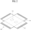
- FIG. 2 is a perspective view illustrating an FPCB substrate which is used for an OLED lighting module according to an exemplary embodiment of the present invention
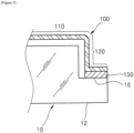
- FIGS. 3 and 4 are cross-sectional views illustrating a combined status of the OLED lighting module according to the exemplary embodiment of the present invention.
- connection terminal is coupled to the transparent electrode using the FPCB substrate and an anisotropic conductive film.
- the exemplary embodiment comprises the above-described OLED illumination plate (10 of FIG. 1 ), an FPCB substrate 100 as illustrated in FIG. 2 , and a conductive adhesive film 150 which couples and electrically conducts the transparent electrode of the OLED illumination plate 10 and the connection terminal 122 of the FPCB substrate as illustrated in FIG. 3 .
- the FPCB substrate 100 comprises a main substrate portion 110 which has a size corresponding to a center surface 14 of the OLED illumination plate 10 and wing substrate portions 120 which are formed to extend in four directions from the main substrate portion 110 and comprise the connection terminal 122 corresponding to the transparent electrode.
- the FPCB substrate 100 comprises a power terminal 101 which is coupled to a power supply of the main substrate portion 110 on a surface opposite to a surface on which the connection terminal 122 is formed.
- the main substrate portion 110 and the wing substrate portions 120 are integrally formed but boundaries of the main substrate portion 110 and the wing substrate portions 120 are represented by one-dot chain lines for the convenience of description.
- the FPCB substrate 100 is attached onto the first surface 12 of the OLED illumination plate 10 so that the transparent electrode of the OLED illumination plate 10 is coupled to the connection terminal 122 of the FPCB substrate 100.
- the transparent electrode of the OLED illumination plate 10 and the connection terminal 122 of the FPCB substrate 100 are adhered and connected to each other by the conductive adhesive film while facing each other.
- connection terminal 122 of the FPCB substrate 100 When the connection terminal 122 of the FPCB substrate 100 is attached to the transparent electrode so as to face each other as described above, the power terminal 101 is disposed on an opposite surface of the attached surface so that the power terminal 101 is exposed to the outside (in FIG. 2 , the power terminal is represented by a dotted line in order to indicate that the power terminal is formed on an opposite surface of the connection terminal. Accordingly, a power line of a power supply (normally, a driving driver) is coupled to the power terminal 101.
- a power line of a power supply normally, a driving driver
- the FPCB substrate 100 is mounted with a circuit pattern which couples the power terminal 101 to the connection terminal 122.
- an anisotropic conductive film which provides electrical conduction only in a direction to which a compressive force is applied and provides a binding force by thermal compression may be used for the conductive adhesive film.
- the wing substrate portion 120 of the FPCB substrate 100 may be bent as an L-shape to be attached onto the border surface 16 of the OLED illumination plate 10.
- a reinforcement member 160 which has a height similar to the step is formed above the wing substrate portion 120 which is attached onto the border surface 16.
- the reinforcement member 160 may be formed by applying a silicon resin or using a separate injection molding product or a rubber packing.
- the OLED lighting module has a rectangular parallelepiped panel shape which does not entirely have a step and thus a subsequent packaging process is easily performed. Further, even when no additional packaging is used, damage may be prevented and the FPCB substrate may be prevented from being peeled off.
- a further OLED lighting module which is not covered by the invention provides a structure in which a flat panel PCB substrate (in order to distinguish from the FPCB, a terminology of a hard PCB substrate is used, but a terminology of a PCB substrate is used in this description) is coupled to a transparent electrode of an OLED light guide plate using a conductive rod which is mounted in the PCB substrate.
- a flat panel PCB substrate in order to distinguish from the FPCB, a terminology of a hard PCB substrate is used, but a terminology of a PCB substrate is used in this description
- FIG. 5 is an exploded perspective view of an OLED lighting module which is not covered by the present invention.
- a PCB substrate 200 has a size corresponding to a first surface 12 of an OLED illumination plate 10 and comprises a power terminal, which is coupled to a power supply, on one surface thereof and a connection terminal 202 in a position corresponding to the transparent electrode on the other surface.
- a conductive rod 210 is mounted on the connection terminal 202.
- one conductive rod 210 may be formed on one side or a plurality of divided conductive rods may be formed on one side.
- the conductive rod 210 has a square column shape and a metal having an excellent conductivity may be used as a material.
- a brass rod may be desirably used.
- a surface of non-metal rod which is enclosed by a conductive member may be used.
- the conductive rod 210 may be mounted in the connection terminal 202 of the PCB substrate 200 by a surface mounting method.
- FIG. 6 is a cross-sectional view of a combining process of the OLED lighting module shown in FIG. 5 .
- a conductive paste 230 is applied in a region where the transparent electrode of the OLED illumination plate 10 is formed and then the PCB substrate 200 in which the conductive rod 210 is mounted is attached.
- a thickness (t) of the conductive rod 210 may correspond to a height (h) of the step of the OLED illumination plate 10.
- the conductive rod 210 When the conductive rod 210 is mounted in the PCB substrate 200 to be attached on the OLED illumination plate 10 as described above, the conductive rod 210 fills the step so as to protect the border of the OLED lighting module.
- the conductive paste 220 is required to have a conductivity and a binding force, so that a silver (Ag) paste may be representatively used.
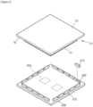
- FIG. 7 is an exploded perspective view of a further OLED lighting module not covered by the present invention.
- the OLED lighting module shown in FIG. 7 provides a structure in that a FPCB substrate is formed to have a frame shape corresponding to a border surface so as to be attached only on the border surface except a center surface of an OLED illumination plate.
- a FPCB substrate is formed to have a frame shape corresponding to a border surface so as to be attached only on the border surface except a center surface of an OLED illumination plate.
- the OLED lighting module is formed such that a frame shaped FPCB substrate 300 is attached to a border surface 16 of an OLED illumination plate 10 using a conductive adhesive film (not illustrated).
- the adhesion structure using the conductive adhesive film is the same as the exemplary embodiment, and thus the redundant description will be omitted.
- the frame shaped FPCB substrate 300 comprises a power terminal 302 which is formed to protrude, on one side.
- the power terminal 302 is formed to outwardly protrude so as to be coupled to the power supply.
- the frame shaped FPCB substrate 300 comprises a connecting FPCB substrate portion 310 which has a length corresponding to a length of each side and has a connection terminal and a coupling FPCB substrate portion 320 which couples adjacent connecting FPCB substrate portions 310 to each other and is formed in an L shape.
- the frame shaped FPCB substrate 300 comprises a positive electrode pattern which is coupled to a positive power terminal and a negative electrode pattern which is coupled to a negative power terminal.
- the frame shaped FPCB substrate 300 may have an arrangement in which the positive electrode pattern is formed inside and the negative electrode pattern is formed outside and vice versa so that two electrode patterns may be formed inside the frame shape.
- the OLED lighting module according to the present invention provides a coupling structure which may stably supply a power to the transparent electrode of the OLED illumination plate so that the quality of the OLED lighting module may be stable.
Landscapes
- Engineering & Computer Science (AREA)
- Microelectronics & Electronic Packaging (AREA)
- Physics & Mathematics (AREA)
- Optics & Photonics (AREA)
- General Engineering & Computer Science (AREA)
- Manufacturing & Machinery (AREA)
- Electroluminescent Light Sources (AREA)
- Arrangement Of Elements, Cooling, Sealing, Or The Like Of Lighting Devices (AREA)
Claims (1)
- Organische-lichtemittierende-Vorrichtung-, OLED-, Beleuchtungsmodul, aufweisend:eine OLED-Beleuchtungsplatte (10), die aufweist: eine erste Fläche (12), die vollständig flach ausgebildet ist, eine zweite Fläche (18), die der ersten Fläche gegenüberliegt und die eine Mittelfläche (14) und eine Randfläche (16) hat, die stufenförmig um die Mittelfläche (14) herum ausgebildet ist, und eine transparente Elektrode, die auf der Stufenfläche (16) ausgebildet ist;ein FPCB-Substrat (100), das aufweist: einen Hauptsubstratabschnitt (110), der einen Stromanschluss (101) aufweist, der konfiguriert ist, um elektrisch mit einer Stromversorgung verbunden zu sein, wobei der Stromanschluss (101) zu der Mittelfläche (14) korrespondiert, und einen Flügelsubstratabschnitt (120), der so ausgebildet ist, dass er sich von der Mittelfläche (14) in vier Richtungen erstreckt, und einen Verbindungsanschluss (122) aufweist, der zu der transparenten Elektrode korrespondiert;ein Verstärkungselement (160), das eine Höhe hat, die gleich wie eine Stufe ist, die über dem Flügelsubstratabschnitt (120) ausgebildet ist, der an der Randfläche (16) angebracht ist,ein Schaltungsmuster, das den Stromanschluss (101) mit dem Verbindungsanschluss (122) verbindet; undeinen leitfähigen Klebefilm (150), der zwischen der Stufenfläche (16) und dem Flügelsubstratabschnitt (120) angebracht ist, um die transparente Elektrode und den Verbindungsanschluss (122) elektrisch zu leiten,wobei der leitfähige Klebefilm (150) ein anisotroper leitfähiger Film ist, der durch thermische Kompression angebracht ist, um eine elektrische Leitung nur in einer Richtung bereitzustellen, in der ein Druck ausgeübt wird.
Applications Claiming Priority (2)
| Application Number | Priority Date | Filing Date | Title |
|---|---|---|---|
| KR1020120102408A KR101514114B1 (ko) | 2012-09-14 | 2012-09-14 | Oled 조명 모듈 |
| PCT/KR2013/008312 WO2014042467A1 (ko) | 2012-09-14 | 2013-09-13 | Oled 조명 모듈 |
Publications (3)
| Publication Number | Publication Date |
|---|---|
| EP2887415A1 EP2887415A1 (de) | 2015-06-24 |
| EP2887415A4 EP2887415A4 (de) | 2016-06-22 |
| EP2887415B1 true EP2887415B1 (de) | 2024-10-30 |
Family
ID=50278480
Family Applications (1)
| Application Number | Title | Priority Date | Filing Date |
|---|---|---|---|
| EP13836856.8A Active EP2887415B1 (de) | 2012-09-14 | 2013-09-13 | Oled-beleuchtungsmodul |
Country Status (7)
| Country | Link |
|---|---|
| US (1) | US9638400B2 (de) |
| EP (1) | EP2887415B1 (de) |
| JP (1) | JP6058143B2 (de) |
| KR (1) | KR101514114B1 (de) |
| CN (1) | CN108119783B (de) |
| TW (1) | TWI524570B (de) |
| WO (1) | WO2014042467A1 (de) |
Families Citing this family (3)
| Publication number | Priority date | Publication date | Assignee | Title |
|---|---|---|---|---|
| WO2017033630A1 (ja) * | 2015-08-26 | 2017-03-02 | 株式会社カネカ | 面状発光装置 |
| TWI603030B (zh) | 2016-12-26 | 2017-10-21 | 機光科技股份有限公司 | Oled平面燈源模組 |
| KR20220069173A (ko) | 2020-11-19 | 2022-05-27 | 삼성디스플레이 주식회사 | 보호 캡 및 이를 포함하는 표시 장치 |
Citations (1)
| Publication number | Priority date | Publication date | Assignee | Title |
|---|---|---|---|---|
| WO2011136262A1 (ja) * | 2010-04-27 | 2011-11-03 | Lumiotec株式会社 | 有機el照明装置 |
Family Cites Families (24)
| Publication number | Priority date | Publication date | Assignee | Title |
|---|---|---|---|---|
| JPH08505000A (ja) | 1992-12-16 | 1996-05-28 | デュレル・コーポレイション | 電界発光ランプ装置とその製造 |
| JP2000243555A (ja) * | 1999-02-17 | 2000-09-08 | Toyota Motor Corp | 有機el表示装置 |
| JP3684169B2 (ja) | 2000-04-21 | 2005-08-17 | キヤノン株式会社 | 固体撮像装置 |
| EP1162045B1 (de) | 2000-05-30 | 2007-03-14 | Andritz Küsters GmbH & Co. KG | Walzenvorrichtung |
| JP3501218B2 (ja) * | 2000-08-11 | 2004-03-02 | 日本電気株式会社 | フラットパネル表示モジュール及びその製造方法 |
| KR100477101B1 (ko) * | 2000-10-06 | 2005-03-17 | 삼성에스디아이 주식회사 | 유기 발광 소자 |
| KR100768182B1 (ko) | 2001-10-26 | 2007-10-17 | 삼성에스디아이 주식회사 | 유기 전자 발광 소자와 그 제조방법 |
| KR20030048802A (ko) | 2001-12-13 | 2003-06-25 | 엘지이노텍 주식회사 | 하이브리드 아이씨의 단자 구조 |
| TWI297095B (en) * | 2003-10-02 | 2008-05-21 | Au Optronics Corp | Bonding pad structure for a display and fabrication method thereof |
| JP4679921B2 (ja) * | 2005-02-15 | 2011-05-11 | 小泉産業株式会社 | El光源体およびel光源装置 |
| KR100747336B1 (ko) | 2006-01-20 | 2007-08-07 | 엘에스전선 주식회사 | 이방성 도전 필름을 이용한 회로기판의 접속 구조체, 이를위한 제조 방법 및 이를 이용한 접속 상태 평가방법 |
| KR20070090523A (ko) | 2006-03-03 | 2007-09-06 | 삼성전자주식회사 | 디스플레이장치 및 그 제조방법 |
| JP2007280693A (ja) * | 2006-04-04 | 2007-10-25 | Koizumi Lighting Technology Corp | El光源体 |
| TWI332812B (en) | 2007-11-28 | 2010-11-01 | Delta Electronics Inc | Circuit board module with surface mount conductive pin and circuit boards assembly having same |
| TW200950178A (en) * | 2008-01-30 | 2009-12-01 | Koninkl Philips Electronics Nv | OLED lighting device |
| DE102008027519A1 (de) * | 2008-06-10 | 2009-12-17 | Fraunhofer-Gesellschaft zur Förderung der angewandten Forschung e.V. | Flächige Leuchtkörper und ein Verfahren zum Kontaktieren flächiger Leuchtkörper |
| JP4570668B2 (ja) * | 2008-06-27 | 2010-10-27 | 財団法人山形県産業技術振興機構 | 照明装置 |
| KR100962218B1 (ko) | 2008-12-01 | 2010-06-11 | 한국생산기술연구원 | 방열배선이 형성된 대면적 oled 조명용 패널 및 이를 위한 저접촉저항 특성을 갖는 등기구 |
| JP5240718B2 (ja) * | 2009-02-20 | 2013-07-17 | パナソニック株式会社 | 有機elモジュール |
| TWI423718B (zh) | 2009-10-21 | 2014-01-11 | Au Optronics Corp | 有機電致發光裝置及具有此有機電致發光裝置的電子裝置 |
| JP5796171B2 (ja) * | 2009-10-27 | 2015-10-21 | パナソニックIpマネジメント株式会社 | 発光モジュール |
| DE102009046755A1 (de) * | 2009-11-17 | 2011-05-26 | Fraunhofer-Gesellschaft zur Förderung der angewandten Forschung e.V. | Organisches photoelektrisches Bauelement |
| JP2011216353A (ja) * | 2010-03-31 | 2011-10-27 | Panasonic Electric Works Co Ltd | 発光装置 |
| TWI591871B (zh) * | 2010-12-16 | 2017-07-11 | 半導體能源研究所股份有限公司 | 發光裝置及照明裝置 |
-
2012
- 2012-09-14 KR KR1020120102408A patent/KR101514114B1/ko active Active
-
2013
- 2013-09-13 US US14/428,226 patent/US9638400B2/en active Active
- 2013-09-13 JP JP2015531859A patent/JP6058143B2/ja active Active
- 2013-09-13 WO PCT/KR2013/008312 patent/WO2014042467A1/ko not_active Ceased
- 2013-09-13 EP EP13836856.8A patent/EP2887415B1/de active Active
- 2013-09-13 CN CN201810060716.9A patent/CN108119783B/zh active Active
- 2013-09-14 TW TW102133325A patent/TWI524570B/zh active
Patent Citations (1)
| Publication number | Priority date | Publication date | Assignee | Title |
|---|---|---|---|---|
| WO2011136262A1 (ja) * | 2010-04-27 | 2011-11-03 | Lumiotec株式会社 | 有機el照明装置 |
Also Published As
| Publication number | Publication date |
|---|---|
| CN108119783A (zh) | 2018-06-05 |
| CN104620403A (zh) | 2015-05-13 |
| EP2887415A1 (de) | 2015-06-24 |
| TW201427135A (zh) | 2014-07-01 |
| KR20140035743A (ko) | 2014-03-24 |
| JP2015534217A (ja) | 2015-11-26 |
| WO2014042467A1 (ko) | 2014-03-20 |
| TWI524570B (zh) | 2016-03-01 |
| EP2887415A4 (de) | 2016-06-22 |
| JP6058143B2 (ja) | 2017-01-11 |
| US20150247626A1 (en) | 2015-09-03 |
| US9638400B2 (en) | 2017-05-02 |
| KR101514114B1 (ko) | 2015-04-21 |
| CN108119783B (zh) | 2020-03-31 |
Similar Documents
| Publication | Publication Date | Title |
|---|---|---|
| EP2566298B1 (de) | Organische el-beleuchtungsvorrichtung | |
| JP4679921B2 (ja) | El光源体およびel光源装置 | |
| KR101303595B1 (ko) | 방열 인쇄회로기판, 방열 인쇄회로기판 제조방법, 방열 인쇄회로기판을 포함하는 백라이트 유닛 및 액정표시장치 | |
| EP2309312B1 (de) | Lichtmodul | |
| TWI556484B (zh) | 有機發光二極體模組 | |
| EP3226321B1 (de) | Organische elektrolumineszenzvorrichtung, herstellungsverfahren dafür sowie anzeigevorrichtung damit | |
| US9638400B2 (en) | OLED lighting module | |
| JP4679922B2 (ja) | El光源体 | |
| EP2993712B1 (de) | Organische lichtemittierende vorrichtung und herstellungsverfahren dafür | |
| TWI684265B (zh) | Led構裝模組及led顯示裝置 | |
| US20060119263A1 (en) | Double-side display device and method of making same | |
| JP4559248B2 (ja) | El光源体およびel光源装置 | |
| WO2020195160A1 (ja) | 有機elパネル | |
| TWI711193B (zh) | Led元件用基板、led構裝模組、及使用該等而得之led顯示裝置 | |
| KR101408384B1 (ko) | Oled 조명 모듈 | |
| CN111048560B (zh) | 显示装置 | |
| CN104620403B (zh) | Oled发光模块 | |
| US20210050323A1 (en) | Electrode connection element, light-emitting device comprising same, and method for producing light-emitting device | |
| WO2013179482A1 (ja) | 有機el発光素子及びその製造方法 | |
| JP2011187217A (ja) | 有機elモジュール | |
| KR102063523B1 (ko) | 조명장치 및 이의 제조 방법 | |
| JP2014179284A (ja) | 有機elモジュール | |
| KR20140145702A (ko) | 조명장치 | |
| TWM384412U (en) | LED display module with a transparent substrate | |
| JP2004319407A (ja) | 有機elパネルの接続構造 |
Legal Events
| Date | Code | Title | Description |
|---|---|---|---|
| PUAI | Public reference made under article 153(3) epc to a published international application that has entered the european phase |
Free format text: ORIGINAL CODE: 0009012 |
|
| 17P | Request for examination filed |
Effective date: 20150312 |
|
| AK | Designated contracting states |
Kind code of ref document: A1 Designated state(s): AL AT BE BG CH CY CZ DE DK EE ES FI FR GB GR HR HU IE IS IT LI LT LU LV MC MK MT NL NO PL PT RO RS SE SI SK SM TR |
|
| AX | Request for extension of the european patent |
Extension state: BA ME |
|
| RIN1 | Information on inventor provided before grant (corrected) |
Inventor name: HEO, DONG-HYUK Inventor name: LIM, SUNG-RYUN Inventor name: KANG, MINSOO Inventor name: OH, DUCKSU |
|
| DAX | Request for extension of the european patent (deleted) | ||
| RAP1 | Party data changed (applicant data changed or rights of an application transferred) |
Owner name: LG DISPLAY CO., LTD. |
|
| RA4 | Supplementary search report drawn up and despatched (corrected) |
Effective date: 20160520 |
|
| RIC1 | Information provided on ipc code assigned before grant |
Ipc: H05B 33/06 20060101ALI20160513BHEP Ipc: H01L 51/50 20060101AFI20160513BHEP Ipc: H05K 3/40 20060101ALI20160513BHEP Ipc: H05K 1/18 20060101ALI20160513BHEP Ipc: H05K 3/32 20060101ALN20160513BHEP Ipc: G02F 1/1345 20060101ALN20160513BHEP |
|
| STAA | Information on the status of an ep patent application or granted ep patent |
Free format text: STATUS: EXAMINATION IS IN PROGRESS |
|
| 17Q | First examination report despatched |
Effective date: 20190111 |
|
| REG | Reference to a national code |
Ref country code: DE Ref legal event code: R079 Free format text: PREVIOUS MAIN CLASS: H01L0051500000 Ipc: H05K0001180000 Ref document number: 602013086241 Country of ref document: DE |
|
| GRAP | Despatch of communication of intention to grant a patent |
Free format text: ORIGINAL CODE: EPIDOSNIGR1 |
|
| STAA | Information on the status of an ep patent application or granted ep patent |
Free format text: STATUS: GRANT OF PATENT IS INTENDED |
|
| RIC1 | Information provided on ipc code assigned before grant |
Ipc: F21Y 115/15 20160101ALN20240403BHEP Ipc: F21Y 105/00 20060101ALN20240403BHEP Ipc: H05K 3/32 20060101ALN20240403BHEP Ipc: H05B 33/28 20060101ALI20240403BHEP Ipc: H05B 33/14 20060101ALI20240403BHEP Ipc: H05B 33/06 20060101ALI20240403BHEP Ipc: H05K 3/40 20060101ALI20240403BHEP Ipc: H05K 1/18 20060101AFI20240403BHEP |
|
| INTG | Intention to grant announced |
Effective date: 20240425 |
|
| GRAS | Grant fee paid |
Free format text: ORIGINAL CODE: EPIDOSNIGR3 |
|
| GRAA | (expected) grant |
Free format text: ORIGINAL CODE: 0009210 |
|
| STAA | Information on the status of an ep patent application or granted ep patent |
Free format text: STATUS: THE PATENT HAS BEEN GRANTED |
|
| AK | Designated contracting states |
Kind code of ref document: B1 Designated state(s): AL AT BE BG CH CY CZ DE DK EE ES FI FR GB GR HR HU IE IS IT LI LT LU LV MC MK MT NL NO PL PT RO RS SE SI SK SM TR |
|
| REG | Reference to a national code |
Ref country code: GB Ref legal event code: FG4D |
|
| REG | Reference to a national code |
Ref country code: CH Ref legal event code: EP |
|
| REG | Reference to a national code |
Ref country code: IE Ref legal event code: FG4D |
|
| REG | Reference to a national code |
Ref country code: DE Ref legal event code: R096 Ref document number: 602013086241 Country of ref document: DE |
|
| REG | Reference to a national code |
Ref country code: LT Ref legal event code: MG9D |
|
| REG | Reference to a national code |
Ref country code: NL Ref legal event code: MP Effective date: 20241030 |
|
| PG25 | Lapsed in a contracting state [announced via postgrant information from national office to epo] |
Ref country code: HR Free format text: LAPSE BECAUSE OF FAILURE TO SUBMIT A TRANSLATION OF THE DESCRIPTION OR TO PAY THE FEE WITHIN THE PRESCRIBED TIME-LIMIT Effective date: 20241030 Ref country code: IS Free format text: LAPSE BECAUSE OF FAILURE TO SUBMIT A TRANSLATION OF THE DESCRIPTION OR TO PAY THE FEE WITHIN THE PRESCRIBED TIME-LIMIT Effective date: 20250228 Ref country code: PT Free format text: LAPSE BECAUSE OF FAILURE TO SUBMIT A TRANSLATION OF THE DESCRIPTION OR TO PAY THE FEE WITHIN THE PRESCRIBED TIME-LIMIT Effective date: 20250228 |
|
| PG25 | Lapsed in a contracting state [announced via postgrant information from national office to epo] |
Ref country code: FI Free format text: LAPSE BECAUSE OF FAILURE TO SUBMIT A TRANSLATION OF THE DESCRIPTION OR TO PAY THE FEE WITHIN THE PRESCRIBED TIME-LIMIT Effective date: 20241030 Ref country code: NL Free format text: LAPSE BECAUSE OF FAILURE TO SUBMIT A TRANSLATION OF THE DESCRIPTION OR TO PAY THE FEE WITHIN THE PRESCRIBED TIME-LIMIT Effective date: 20241030 |
|
| REG | Reference to a national code |
Ref country code: AT Ref legal event code: MK05 Ref document number: 1738228 Country of ref document: AT Kind code of ref document: T Effective date: 20241030 |
|
| PG25 | Lapsed in a contracting state [announced via postgrant information from national office to epo] |
Ref country code: BG Free format text: LAPSE BECAUSE OF FAILURE TO SUBMIT A TRANSLATION OF THE DESCRIPTION OR TO PAY THE FEE WITHIN THE PRESCRIBED TIME-LIMIT Effective date: 20241030 |
|
| PG25 | Lapsed in a contracting state [announced via postgrant information from national office to epo] |
Ref country code: ES Free format text: LAPSE BECAUSE OF FAILURE TO SUBMIT A TRANSLATION OF THE DESCRIPTION OR TO PAY THE FEE WITHIN THE PRESCRIBED TIME-LIMIT Effective date: 20241030 |
|
| PG25 | Lapsed in a contracting state [announced via postgrant information from national office to epo] |
Ref country code: NO Free format text: LAPSE BECAUSE OF FAILURE TO SUBMIT A TRANSLATION OF THE DESCRIPTION OR TO PAY THE FEE WITHIN THE PRESCRIBED TIME-LIMIT Effective date: 20250130 |
|
| PG25 | Lapsed in a contracting state [announced via postgrant information from national office to epo] |
Ref country code: LV Free format text: LAPSE BECAUSE OF FAILURE TO SUBMIT A TRANSLATION OF THE DESCRIPTION OR TO PAY THE FEE WITHIN THE PRESCRIBED TIME-LIMIT Effective date: 20241030 Ref country code: AT Free format text: LAPSE BECAUSE OF FAILURE TO SUBMIT A TRANSLATION OF THE DESCRIPTION OR TO PAY THE FEE WITHIN THE PRESCRIBED TIME-LIMIT Effective date: 20241030 Ref country code: GR Free format text: LAPSE BECAUSE OF FAILURE TO SUBMIT A TRANSLATION OF THE DESCRIPTION OR TO PAY THE FEE WITHIN THE PRESCRIBED TIME-LIMIT Effective date: 20250131 |
|
| PG25 | Lapsed in a contracting state [announced via postgrant information from national office to epo] |
Ref country code: PL Free format text: LAPSE BECAUSE OF FAILURE TO SUBMIT A TRANSLATION OF THE DESCRIPTION OR TO PAY THE FEE WITHIN THE PRESCRIBED TIME-LIMIT Effective date: 20241030 |
|
| PG25 | Lapsed in a contracting state [announced via postgrant information from national office to epo] |
Ref country code: RS Free format text: LAPSE BECAUSE OF FAILURE TO SUBMIT A TRANSLATION OF THE DESCRIPTION OR TO PAY THE FEE WITHIN THE PRESCRIBED TIME-LIMIT Effective date: 20250130 |
|
| PG25 | Lapsed in a contracting state [announced via postgrant information from national office to epo] |
Ref country code: SM Free format text: LAPSE BECAUSE OF FAILURE TO SUBMIT A TRANSLATION OF THE DESCRIPTION OR TO PAY THE FEE WITHIN THE PRESCRIBED TIME-LIMIT Effective date: 20241030 |
|
| PG25 | Lapsed in a contracting state [announced via postgrant information from national office to epo] |
Ref country code: DK Free format text: LAPSE BECAUSE OF FAILURE TO SUBMIT A TRANSLATION OF THE DESCRIPTION OR TO PAY THE FEE WITHIN THE PRESCRIBED TIME-LIMIT Effective date: 20241030 |
|
| PG25 | Lapsed in a contracting state [announced via postgrant information from national office to epo] |
Ref country code: EE Free format text: LAPSE BECAUSE OF FAILURE TO SUBMIT A TRANSLATION OF THE DESCRIPTION OR TO PAY THE FEE WITHIN THE PRESCRIBED TIME-LIMIT Effective date: 20241030 |
|
| PG25 | Lapsed in a contracting state [announced via postgrant information from national office to epo] |
Ref country code: RO Free format text: LAPSE BECAUSE OF FAILURE TO SUBMIT A TRANSLATION OF THE DESCRIPTION OR TO PAY THE FEE WITHIN THE PRESCRIBED TIME-LIMIT Effective date: 20241030 |
|
| PG25 | Lapsed in a contracting state [announced via postgrant information from national office to epo] |
Ref country code: SK Free format text: LAPSE BECAUSE OF FAILURE TO SUBMIT A TRANSLATION OF THE DESCRIPTION OR TO PAY THE FEE WITHIN THE PRESCRIBED TIME-LIMIT Effective date: 20241030 |
|
| PG25 | Lapsed in a contracting state [announced via postgrant information from national office to epo] |
Ref country code: CZ Free format text: LAPSE BECAUSE OF FAILURE TO SUBMIT A TRANSLATION OF THE DESCRIPTION OR TO PAY THE FEE WITHIN THE PRESCRIBED TIME-LIMIT Effective date: 20241030 |
|
| PG25 | Lapsed in a contracting state [announced via postgrant information from national office to epo] |
Ref country code: IT Free format text: LAPSE BECAUSE OF FAILURE TO SUBMIT A TRANSLATION OF THE DESCRIPTION OR TO PAY THE FEE WITHIN THE PRESCRIBED TIME-LIMIT Effective date: 20241030 |
|
| REG | Reference to a national code |
Ref country code: DE Ref legal event code: R097 Ref document number: 602013086241 Country of ref document: DE |
|
| PLBE | No opposition filed within time limit |
Free format text: ORIGINAL CODE: 0009261 |
|
| STAA | Information on the status of an ep patent application or granted ep patent |
Free format text: STATUS: NO OPPOSITION FILED WITHIN TIME LIMIT |
|
| PG25 | Lapsed in a contracting state [announced via postgrant information from national office to epo] |
Ref country code: SE Free format text: LAPSE BECAUSE OF FAILURE TO SUBMIT A TRANSLATION OF THE DESCRIPTION OR TO PAY THE FEE WITHIN THE PRESCRIBED TIME-LIMIT Effective date: 20241030 |
|
| 26N | No opposition filed |
Effective date: 20250731 |
|
| PGFP | Annual fee paid to national office [announced via postgrant information from national office to epo] |
Ref country code: DE Payment date: 20250721 Year of fee payment: 13 |
|
| PGFP | Annual fee paid to national office [announced via postgrant information from national office to epo] |
Ref country code: GB Payment date: 20250722 Year of fee payment: 13 |
|
| PGFP | Annual fee paid to national office [announced via postgrant information from national office to epo] |
Ref country code: FR Payment date: 20250725 Year of fee payment: 13 |
|
| REG | Reference to a national code |
Ref country code: CH Ref legal event code: H13 Free format text: ST27 STATUS EVENT CODE: U-0-0-H10-H13 (AS PROVIDED BY THE NATIONAL OFFICE) Effective date: 20260504 |