EP2879168A1 - Method for removing polycrystalline silicon protecting layer on igbt back face having field termination structure - Google Patents
Method for removing polycrystalline silicon protecting layer on igbt back face having field termination structure Download PDFInfo
- Publication number
- EP2879168A1 EP2879168A1 EP13822946.3A EP13822946A EP2879168A1 EP 2879168 A1 EP2879168 A1 EP 2879168A1 EP 13822946 A EP13822946 A EP 13822946A EP 2879168 A1 EP2879168 A1 EP 2879168A1
- Authority
- EP
- European Patent Office
- Prior art keywords
- layer
- sio
- protection layer
- back face
- gate oxide
- Prior art date
- Legal status (The legal status is an assumption and is not a legal conclusion. Google has not performed a legal analysis and makes no representation as to the accuracy of the status listed.)
- Granted
Links
Images


Classifications
-
- H—ELECTRICITY
- H10—SEMICONDUCTOR DEVICES; ELECTRIC SOLID-STATE DEVICES NOT OTHERWISE PROVIDED FOR
- H10D—INORGANIC ELECTRIC SEMICONDUCTOR DEVICES
- H10D12/00—Bipolar devices controlled by the field effect, e.g. insulated-gate bipolar transistors [IGBT]
- H10D12/411—Insulated-gate bipolar transistors [IGBT]
- H10D12/441—Vertical IGBTs
-
- H—ELECTRICITY
- H10—SEMICONDUCTOR DEVICES; ELECTRIC SOLID-STATE DEVICES NOT OTHERWISE PROVIDED FOR
- H10P—GENERIC PROCESSES OR APPARATUS FOR THE MANUFACTURE OR TREATMENT OF DEVICES COVERED BY CLASS H10
- H10P50/00—Etching of wafers, substrates or parts of devices
- H10P50/20—Dry etching; Plasma etching; Reactive-ion etching
- H10P50/28—Dry etching; Plasma etching; Reactive-ion etching of insulating materials
- H10P50/282—Dry etching; Plasma etching; Reactive-ion etching of insulating materials of inorganic materials
- H10P50/283—Dry etching; Plasma etching; Reactive-ion etching of insulating materials of inorganic materials by chemical means
-
- H—ELECTRICITY
- H10—SEMICONDUCTOR DEVICES; ELECTRIC SOLID-STATE DEVICES NOT OTHERWISE PROVIDED FOR
- H10D—INORGANIC ELECTRIC SEMICONDUCTOR DEVICES
- H10D12/00—Bipolar devices controlled by the field effect, e.g. insulated-gate bipolar transistors [IGBT]
- H10D12/01—Manufacture or treatment
-
- H—ELECTRICITY
- H10—SEMICONDUCTOR DEVICES; ELECTRIC SOLID-STATE DEVICES NOT OTHERWISE PROVIDED FOR
- H10D—INORGANIC ELECTRIC SEMICONDUCTOR DEVICES
- H10D12/00—Bipolar devices controlled by the field effect, e.g. insulated-gate bipolar transistors [IGBT]
- H10D12/01—Manufacture or treatment
- H10D12/031—Manufacture or treatment of IGBTs
- H10D12/032—Manufacture or treatment of IGBTs of vertical IGBTs
-
- H—ELECTRICITY
- H10—SEMICONDUCTOR DEVICES; ELECTRIC SOLID-STATE DEVICES NOT OTHERWISE PROVIDED FOR
- H10P—GENERIC PROCESSES OR APPARATUS FOR THE MANUFACTURE OR TREATMENT OF DEVICES COVERED BY CLASS H10
- H10P50/00—Etching of wafers, substrates or parts of devices
- H10P50/20—Dry etching; Plasma etching; Reactive-ion etching
- H10P50/26—Dry etching; Plasma etching; Reactive-ion etching of conductive or resistive materials
- H10P50/264—Dry etching; Plasma etching; Reactive-ion etching of conductive or resistive materials by chemical means
- H10P50/266—Dry etching; Plasma etching; Reactive-ion etching of conductive or resistive materials by chemical means by vapour etching only
- H10P50/267—Dry etching; Plasma etching; Reactive-ion etching of conductive or resistive materials by chemical means by vapour etching only using plasmas
- H10P50/268—Dry etching; Plasma etching; Reactive-ion etching of conductive or resistive materials by chemical means by vapour etching only using plasmas of silicon-containing layers
-
- H—ELECTRICITY
- H10—SEMICONDUCTOR DEVICES; ELECTRIC SOLID-STATE DEVICES NOT OTHERWISE PROVIDED FOR
- H10P—GENERIC PROCESSES OR APPARATUS FOR THE MANUFACTURE OR TREATMENT OF DEVICES COVERED BY CLASS H10
- H10P14/00—Formation of materials, e.g. in the shape of layers or pillars
- H10P14/60—Formation of materials, e.g. in the shape of layers or pillars of insulating materials
- H10P14/63—Formation of materials, e.g. in the shape of layers or pillars of insulating materials characterised by the formation processes
- H10P14/6302—Non-deposition formation processes
- H10P14/6304—Formation by oxidation, e.g. oxidation of the substrate
- H10P14/6306—Formation by oxidation, e.g. oxidation of the substrate of the semiconductor materials
- H10P14/6308—Formation by oxidation, e.g. oxidation of the substrate of the semiconductor materials of Group IV semiconductors
Definitions
- the present invention relates to semiconductor technology, and in particular to a process for removing a polysilicon protection layer on a back face of an IGBT structure having a field stop structure.
- IGBT Insulated Gate Bipolar Transistor
- a bipolar transistor and an insulated gate field effect transistor, and it has the advantages of both high input impedance characteristic of MOSFET and low forward voltage drop characteristic of GTR, and is characterized by low drive power and low saturation voltage drop. Therefore, IGBT is quite applicable to converter systems with a direct voltage of 600V or above, such as alternating current dynamos, variable-frequency drives, switch-mode power supplies, lighting circuits, traction drives and other areas.
- a silicon dioxide (SiO 2 ) layer and a polysilicon protection layer on the back face of the IGBT having an FS (Field Stop) structure are removed by means of wet etching of silicon on the back face (SEZ) in the backend process of the entire manufacturing process.
- SEZ wet etching of silicon on the back face
- the present invention provides a method for removing a polysilicon protection layer on a back face of an IGBT having a field sop structure.
- the method comprises thermally oxidizing the polysilicon protection layer on the back face of the IGBT until the oxidation is terminated on a gate oxide layer located above the polysilicon protection layer to form a SiO 2 layer, and removing the formed SiO 2 layer and the gate oxide layer by a dry etching process.
- the present invention further provides a method for removing a polysilicon protection layer on a back face of an IGBT having a field stop structure, wherein the method comprises the following steps: a) thermally oxidizing a portion of the polysilicon protection layer to form a SiO 2 layer; b) removing the formed SiO 2 layer by a dry etching process; c) repeating the steps a) and b), until the thermal oxidation process in step a) is terminated on a gate oxide layer located above the polysilicon protection layer; and removing the last formed SiO 2 layer and the gate oxide layer by a dry etching process.
- the present invention further provides a method for forming an IGBT structure, which comprises removing a polysilicon protection layer and a gate oxide layer by the above mentioned methods, implanting ions into a face where the polysilicon protection layer and the gate oxide layer have been removed so as to form a P+ layer, and depositing a metal formed layer on the formed P+ layer.
- the removal of the polysilicon protection layer avoids the risk of metal contamination.
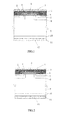
- Fig. 1 illustrates an IGBT structure having a back face protection layer.
- the IGBT structure comprises a surface passivation layer 1, a metal layer 2, a dielectric layer 3, a polysilicon layer 4, a gate oxide layer 5, a P+ layer 6, an N+ layer 7, a P-body layer 8, a drift region 9; a field stop layer 10, a gate oxide layer 11; and a polysilicon protection layer 12.
- the polysilicon protection layer 12 is thermally oxidized to become SiO 2 completely, wherein the thermal oxidation is a conventional thermal oxidation method, for example, atmospheric pressure oxidation or high pressure oxidation.
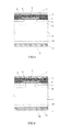
- Fig. 2 illustrates an IGBT structure wherein the polysilicon protection layer 12 has been oxidized to form a SiO 2 layer 13.
- the SiO 2 layer 13 thus formed and the gate oxide layer 11 already formed in Fig. 1 are removed by a dry etching process, wherein dry etching may be plasma etching, ion beam burnishing or reactive ion etching (RIE).
- dry etching may be plasma etching, ion beam burnishing or reactive ion etching (RIE).
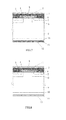
- FIG. 3 illustrates an IGBT structure wherein the SiO 2 layer 13 and the gate oxide layer 11 have been etched off. Afterwards, a P+ layer is formed by ion implantation on the back face, and then, metal deposition is performed on the back face by a method of, for example, evaporation deposition, hence the whole device structure is formed, wherein the ions forming the P+ layer are trivalent ions, such as boron.
- Fig. 4 illustrates an IGBT structure including a P+ layer 14 and a metal layer 15.
- the polysilicon protection layer is oxidized to form the SiO 2 layer by means of thermal oxidation, which, as compared to the conventional SEZ method, prevents the problem of corroding the field stop layer 10.
- the oxidation of the polysilicon protection layer 12 and the removal of the SiO 2 layer 13 and the gate oxide layer 11 occur before formation of the metal layer, the risk of metal contamination is also avoided.
- Fig. 5 illustrates an IGBT structure having a back face protection layer.
- the IGBT structure comprises a surface passivation layer 1, a metal layer 2, a dielectric layer 3, a polysilicon layer 4, a gate oxide layer 5, a P+ layer 6, an N+ layer 7, a Pbody layer 8, a drift region 9; a field stop layer 10, a gate oxide layer 11; and a polysilicon protection layer 12.
- a portion of the polysilicon protection layer 12 is thermally oxidized to SiO 2 , wherein thermal oxidation is a conventional thermal oxidation method, for example, atmospheric pressure oxidation or high pressure oxidation.
- thermal oxidation is a conventional thermal oxidation method, for example, atmospheric pressure oxidation or high pressure oxidation.
- FIG. 6 illustrates an IGBT structure wherein a portion of the polysilicon protection layer 12 has been thermally oxidized to form a SiO 2 layer 13. Afterwards, the SiO 2 layer 13 is etched off by a dry etching process, wherein dry etching may be plasma etching, ion beam burnishing or reactive ion etching (RIE).
- Fig. 7 illustrates an IGBT structure wherein the SiO 2 layer 13 has been removed. As compared to that of the IGBT structure shown in Fig. 5 , the polysilicon protection layer 12 of the IGBT structure shown in Fig. 7 has become thinner. A further portion of the polysilicon protection layer 12 in the structure shown in Fig.
- Fig. 8 illustrates an IGBT structure wherein the last polysilicon protection layer 12 has been thermally oxidized to form a last SiO 2 layer 13. The last SiO 2 layer 13 and the gate oxide layer 11 are removed by means of dry etching to form a IGBT structure as shown in Fig.
- Fig. 10 illustrates an IGBT structure including a P+ layer 14 and a metal layer 15.
- the method in this example employs a thermal oxidation process to oxidize the polysilicon protection layer to form a SiO 2 layer, thus preventing the problem of corroding the field stop layer 10.
- the oxidation of the polysilicon protection layer 12 and the removal of the SiO 2 layer 13 and the gate oxide layer 11 occur before formation of the metal layer, the risk of metal contamination is also avoided.
- Example 2 employs multiple times of oxidation as well as multiple times of dry etching, and therefore, is more applicable to a structure with a thicker polysilicon protection layer.
- the present invention employs a method of thermal oxidation to transform the polysilicon on the back face gradually into SiO 2 , and, due to a barrier effect of SiO 2 , oxidation of the polysilicon protection layer is terminated on the back face oxide layer.
- the back face SiO 2 is removed by a dry etching process, which may not only be compatible with the conventional IGBT process and save costs, but also guarantee that the back face FS layer will be not etched, so as to ensure sufficient thickness of the FS layer, hence it is well guaranteed that the performance parameters of device will not be affected.
- the back face described above refers to a face on which the metal layer 15 is formed.
- the back face SiO 2 refers to the SiO 2 layer 13 described above.
Landscapes
- Electrodes Of Semiconductors (AREA)
- Semiconductor Integrated Circuits (AREA)
- Formation Of Insulating Films (AREA)
Abstract
Description
- The present invention relates to semiconductor technology, and in particular to a process for removing a polysilicon protection layer on a back face of an IGBT structure having a field stop structure.
- IGBT (Insulated Gate Bipolar Transistor) is a compound full-controlled voltage-driven power semiconductor device composed of a bipolar transistor and an insulated gate field effect transistor, and it has the advantages of both high input impedance characteristic of MOSFET and low forward voltage drop characteristic of GTR, and is characterized by low drive power and low saturation voltage drop. Therefore, IGBT is quite applicable to converter systems with a direct voltage of 600V or above, such as alternating current dynamos, variable-frequency drives, switch-mode power supplies, lighting circuits, traction drives and other areas.
- In a manufacturing process of an IGBT, a silicon dioxide (SiO2) layer and a polysilicon protection layer on the back face of the IGBT having an FS (Field Stop) structure are removed by means of wet etching of silicon on the back face (SEZ) in the backend process of the entire manufacturing process. As this conventional removing method is implemented in the backend process where a front face metal layer has already been formed, there is a risk of metal contamination. In addition, since SEZ can etch silicon, it may be easy to corrode the formed field stop layer due to inadequate control when removing the SiO2 layer.
- In view of the foregoing, the present invention provides a method for removing a polysilicon protection layer on a back face of an IGBT having a field sop structure. The method comprises thermally oxidizing the polysilicon protection layer on the back face of the IGBT until the oxidation is terminated on a gate oxide layer located above the polysilicon protection layer to form a SiO2 layer, and removing the formed SiO2 layer and the gate oxide layer by a dry etching process.
- The present invention further provides a method for removing a polysilicon protection layer on a back face of an IGBT having a field stop structure, wherein the method comprises the following steps: a) thermally oxidizing a portion of the polysilicon protection layer to form a SiO2 layer; b) removing the formed SiO2 layer by a dry etching process; c) repeating the steps a) and b), until the thermal oxidation process in step a) is terminated on a gate oxide layer located above the polysilicon protection layer; and removing the last formed SiO2 layer and the gate oxide layer by a dry etching process.
- The present invention further provides a method for forming an IGBT structure, which comprises removing a polysilicon protection layer and a gate oxide layer by the above mentioned methods, implanting ions into a face where the polysilicon protection layer and the gate oxide layer have been removed so as to form a P+ layer, and depositing a metal formed layer on the formed P+ layer.
- According to the method of the present invention, the removal of the polysilicon protection layer avoids the risk of metal contamination.
-
-
Fig. 1 illustrates an IGBT structure having a back face protection layer. -
Fig. 2 illustrates an IGBT structure wherein apolysilicon protection layer 12 has been oxidized to form a SiO2 layer 13. -
Fig. 3 illustrates an IGBT structure wherein the SiO2 layer 13 and agate oxide layer 11 have been etched off. -
Fig. 4 illustrates an IGBT structure including aP+ layer 14 and ametal layer 15. -
Fig. 5 illustrates an IGBT structure having a back face protection layer. -
Fig. 6 illustrates an IGBT structure wherein a portion of thepolysilicon protection layer 12 in the IGBT structure as shown inFig. 5 has been oxidized to form a SiO2 layer 13. -
Fig. 7 illustrates an IGBT structure wherein the SiO2 layer 13 as shown inFig. 6 has been removed. -
Fig. 8 illustrates an IGBT structure wherein the lastpolysilicon protection layer 12 left after multiple times of thermal oxidation in the structure as shown in Fig. has been thermally oxidized to form a last SiO2 layer 13. -
Fig. 9 illustrates an IGBT structure wherein thegate oxide layer 11 and thepolysilicon protection layer 12 in the structure as shown inFig. 5 have been removed. -
Fig. 10 illustrates an IGBT structure wherein aP+ layer 14 and ametal layer 15 have been formed in the IGBT structure as shown inFig. 9 . - Now a further description of the present invention will be made in combination with the accompanying drawings. Those skilled in the art would appreciate that, the following discussion is merely non-limiting explanation of the subject of the present invention in combination with specific implementations, the scope claimed by the present invention shall be defined by the appended claims and any modification or change without departing from the spirit of the present invention shall fall within the scope defined by the claims of the present invention.
- In the descriptions hereinafter, the same layers will be indicated by the same reference numbers in the accompanying drawings.
-
Fig. 1 illustrates an IGBT structure having a back face protection layer. As shown inFig. 1 , the IGBT structure comprises asurface passivation layer 1, ametal layer 2, a dielectric layer 3, a polysilicon layer 4, agate oxide layer 5, aP+ layer 6, anN+ layer 7, a P-body layer 8, adrift region 9; afield stop layer 10, agate oxide layer 11; and apolysilicon protection layer 12. According to this embodiment, thepolysilicon protection layer 12 is thermally oxidized to become SiO2 completely, wherein the thermal oxidation is a conventional thermal oxidation method, for example, atmospheric pressure oxidation or high pressure oxidation. Due to a barrier effect of the gate oxide layer 11 (which is an oxide dielectric layer formed by SiO2), oxidation of thepolysilicon protection layer 12 may be terminated because of contact with thegate oxide layer 11 after polysilicon has been oxidized completely.Fig. 2 illustrates an IGBT structure wherein thepolysilicon protection layer 12 has been oxidized to form a SiO2 layer 13. According to this embodiment of the present invention, after thepolysilicon protection layer 12 has been oxidized to become the SiO2 layer 13, the SiO2 layer 13 thus formed and thegate oxide layer 11 already formed inFig. 1 are removed by a dry etching process, wherein dry etching may be plasma etching, ion beam burnishing or reactive ion etching (RIE).Fig. 3 illustrates an IGBT structure wherein the SiO2 layer 13 and thegate oxide layer 11 have been etched off. Afterwards, a P+ layer is formed by ion implantation on the back face, and then, metal deposition is performed on the back face by a method of, for example, evaporation deposition, hence the whole device structure is formed, wherein the ions forming the P+ layer are trivalent ions, such as boron.Fig. 4 illustrates an IGBT structure including aP+ layer 14 and ametal layer 15. - According to the method described above, the polysilicon protection layer is oxidized to form the SiO2 layer by means of thermal oxidation, which, as compared to the conventional SEZ method, prevents the problem of corroding the
field stop layer 10. In addition, as the oxidation of thepolysilicon protection layer 12 and the removal of the SiO2 layer 13 and thegate oxide layer 11 occur before formation of the metal layer, the risk of metal contamination is also avoided. - As in
Fig. 1 ,Fig. 5 illustrates an IGBT structure having a back face protection layer. As shown in the figure, the IGBT structure comprises asurface passivation layer 1, ametal layer 2, a dielectric layer 3, a polysilicon layer 4, agate oxide layer 5, aP+ layer 6, anN+ layer 7, aPbody layer 8, adrift region 9; afield stop layer 10, agate oxide layer 11; and apolysilicon protection layer 12. According to this embodiment, a portion of thepolysilicon protection layer 12 is thermally oxidized to SiO2, wherein thermal oxidation is a conventional thermal oxidation method, for example, atmospheric pressure oxidation or high pressure oxidation.Fig. 6 illustrates an IGBT structure wherein a portion of thepolysilicon protection layer 12 has been thermally oxidized to form a SiO2 layer 13. Afterwards, the SiO2 layer 13 is etched off by a dry etching process, wherein dry etching may be plasma etching, ion beam burnishing or reactive ion etching (RIE).Fig. 7 illustrates an IGBT structure wherein the SiO2 layer 13 has been removed. As compared to that of the IGBT structure shown inFig. 5 , thepolysilicon protection layer 12 of the IGBT structure shown inFig. 7 has become thinner. A further portion of thepolysilicon protection layer 12 in the structure shown inFig. 7 is oxidized to become the SiO2 layer 13, and then the SiO2 layer is removed by means of dry etching. This process is repeated until the last remainingpolysilicon protection layer 12 is thermally oxidized finally. Due to a barrier effect of the gate oxide layer 11 (which is an oxidate dielectric layer formed by SiO2), oxidation of the remainingpolysilicon protection layer 12 may be terminated because of contact with thegate oxide layer 11 after polysilicon has been oxidized completely.Fig. 8 illustrates an IGBT structure wherein the lastpolysilicon protection layer 12 has been thermally oxidized to form a last SiO2 layer 13. The last SiO2 layer 13 and thegate oxide layer 11 are removed by means of dry etching to form a IGBT structure as shown inFig. 9 , which, when compared with the structure shown inFig. 5 , does not include thegate oxide layer 11 and thepolysilicon protection layer 12. Afterwards, a P+ layer is formed by ion implantation on the back face, and then, metal deposition is performed on the back face by a method of, for example, evaporation deposition, hence the whole device structure is formed, wherein the ions forming the P+ layer are trivalent ions, such as boron.Fig. 10 illustrates an IGBT structure including aP+ layer 14 and ametal layer 15. - Similar to Example 1, as compared to the conventional SEZ method, the method in this example employs a thermal oxidation process to oxidize the polysilicon protection layer to form a SiO2 layer, thus preventing the problem of corroding the
field stop layer 10. In addition, as the oxidation of thepolysilicon protection layer 12 and the removal of the SiO2 layer 13 and thegate oxide layer 11 occur before formation of the metal layer, the risk of metal contamination is also avoided. - The method in Example 2 employs multiple times of oxidation as well as multiple times of dry etching, and therefore, is more applicable to a structure with a thicker polysilicon protection layer.
- In a word, the present invention employs a method of thermal oxidation to transform the polysilicon on the back face gradually into SiO2, and, due to a barrier effect of SiO2, oxidation of the polysilicon protection layer is terminated on the back face oxide layer. Afterwards, the back face SiO2 is removed by a dry etching process, which may not only be compatible with the conventional IGBT process and save costs, but also guarantee that the back face FS layer will be not etched, so as to ensure sufficient thickness of the FS layer, hence it is well guaranteed that the performance parameters of device will not be affected. The back face described above refers to a face on which the
metal layer 15 is formed. The back face SiO2 refers to the SiO2 layer 13 described above.
Claims (3)
- A method for removing a polysilicon protection layer on a back face of an IGBT having a field stop structure, comprising:thermally oxidizing the polysilicon protection layer on the back face of the IGBT until the oxidation is terminated on a gate oxide layer located above the polysilicon protection layer to form a SiO2 layer; andremoving the formed SiO2 layer and the gate oxide layer by a dry etching process.
- A method for removing a polysilicon protection layer on a back face of an IGBT having a field stop structure, comprising the following steps:a) thermally oxidizing a portion of the polysilicon protection layer to form a SiO2 layer;b) removing the formed SiO2 layer by a dry etching process;c) repeating the steps a) and b), until the thermal oxidation process in step a) is terminated on a gate oxide layer located above the polysilicon protection layer; and
removing the last formed SiO2 layer and the gate oxide layer by a dry etching process. - A method for forming an IGBT structure, wherein the method comprises removing a polysilicon protection layer and a gate oxide layer by the method according to claim 1 or 2, and
implanting ions into a face where the polysilicon protection layer and the gate oxide layer have been removed so as to form a P+ layer, and
depositing a metal formed layer on the formed P+ layer.
Applications Claiming Priority (2)
| Application Number | Priority Date | Filing Date | Title |
|---|---|---|---|
| CN201210260773.4A CN103578972B (en) | 2012-07-26 | 2012-07-26 | There is the minimizing technology of the IGBT back side polysilicon protection layer of a termination structure |
| PCT/CN2013/080150 WO2014015821A1 (en) | 2012-07-26 | 2013-07-25 | Method for removing polycrystalline silicon protecting layer on igbt back face having field termination structure |
Publications (3)
| Publication Number | Publication Date |
|---|---|
| EP2879168A1 true EP2879168A1 (en) | 2015-06-03 |
| EP2879168A4 EP2879168A4 (en) | 2016-03-02 |
| EP2879168B1 EP2879168B1 (en) | 2021-03-10 |
Family
ID=49996611
Family Applications (1)
| Application Number | Title | Priority Date | Filing Date |
|---|---|---|---|
| EP13822946.3A Active EP2879168B1 (en) | 2012-07-26 | 2013-07-25 | Method for removing polycrystalline silicon protecting layer on igbt back face having field termination structure |
Country Status (4)
| Country | Link |
|---|---|
| US (1) | US9607851B2 (en) |
| EP (1) | EP2879168B1 (en) |
| CN (1) | CN103578972B (en) |
| WO (1) | WO2014015821A1 (en) |
Families Citing this family (1)
| Publication number | Priority date | Publication date | Assignee | Title |
|---|---|---|---|---|
| CN106783568A (en) * | 2016-12-27 | 2017-05-31 | 株洲中车时代电气股份有限公司 | A kind of power device grid curb wall preparation method |
Family Cites Families (9)
| Publication number | Priority date | Publication date | Assignee | Title |
|---|---|---|---|---|
| US6309929B1 (en) * | 2000-09-22 | 2001-10-30 | Industrial Technology Research Institute And Genetal Semiconductor Of Taiwan, Ltd. | Method of forming trench MOS device and termination structure |
| US6396090B1 (en) * | 2000-09-22 | 2002-05-28 | Industrial Technology Research Institute | Trench MOS device and termination structure |
| JP3559971B2 (en) * | 2001-12-11 | 2004-09-02 | 日産自動車株式会社 | Silicon carbide semiconductor device and method of manufacturing the same |
| TWI235407B (en) * | 2004-05-10 | 2005-07-01 | Mosel Vitelic Inc | Wafer and the manufacturing and reclaiming method therefor |
| JP2007066944A (en) * | 2005-08-29 | 2007-03-15 | Nissan Motor Co Ltd | Silicon carbide semiconductor device and manufacturing method thereof |
| KR100902586B1 (en) * | 2007-06-04 | 2009-06-11 | 주식회사 동부하이텍 | How to remove polysilicon |
| CN101752415A (en) * | 2008-12-03 | 2010-06-23 | 上海芯能电子科技有限公司 | Insulated gate bipolar transistor and method for producing same |
| CN101759140B (en) * | 2008-12-24 | 2013-03-20 | 中国科学院半导体研究所 | Method for manufacturing silicon nano structure |
| CN102142372B (en) * | 2010-12-24 | 2012-10-24 | 江苏宏微科技有限公司 | Preparation method of field blocking type bipolar transistor of insulated gate |
-
2012
- 2012-07-26 CN CN201210260773.4A patent/CN103578972B/en active Active
-
2013
- 2013-07-25 WO PCT/CN2013/080150 patent/WO2014015821A1/en not_active Ceased
- 2013-07-25 EP EP13822946.3A patent/EP2879168B1/en active Active
- 2013-07-25 US US14/411,978 patent/US9607851B2/en active Active
Also Published As
| Publication number | Publication date |
|---|---|
| CN103578972A (en) | 2014-02-12 |
| WO2014015821A1 (en) | 2014-01-30 |
| US20150155182A1 (en) | 2015-06-04 |
| EP2879168A4 (en) | 2016-03-02 |
| CN103578972B (en) | 2016-06-29 |
| EP2879168B1 (en) | 2021-03-10 |
| US9607851B2 (en) | 2017-03-28 |
Similar Documents
| Publication | Publication Date | Title |
|---|---|---|
| US9691863B2 (en) | Self-aligned contact for trench power MOSFET | |
| JP2015015486A (en) | Manufacturing method of trench gate type semiconductor device | |
| US9755028B2 (en) | Semiconductor device and method for manufacturing the same | |
| CN105514022B (en) | The method that portion surface forms field silica in the trench | |
| CN102110602A (en) | Method of manufacturing semiconductor device | |
| US11201088B2 (en) | Semiconductor device and method for forming the same | |
| JP2018117081A (en) | Manufacturing method of semiconductor device | |
| CN104701148A (en) | Method for manufacturing split gate | |
| US9607851B2 (en) | Method for removing polysilicon protection layer on a back face of an IGBT having a field stop structure | |
| US9716159B1 (en) | Method of manufacturing silicon carbide semiconductor device | |
| TW200903654A (en) | Method of forming a gate oxide layer | |
| US10991537B2 (en) | Vertical vacuum channel transistor | |
| WO2014203881A1 (en) | Method for manufacturing silicon carbide semiconductor element | |
| JP2007311547A (en) | Manufacturing method of semiconductor device | |
| JP6235298B2 (en) | Semiconductor device and manufacturing method thereof | |
| KR100948307B1 (en) | Method of manufacturing the semiconductor device | |
| CN103377893B (en) | The method of manufacturing technology of DDMOS step gate oxide | |
| JP7151620B2 (en) | Semiconductor device manufacturing method | |
| KR100351911B1 (en) | Method for forming gate spacer of semiconductor device | |
| CN101211817A (en) | Method for diminishing shallow slot isolation margin depression | |
| KR20040038117A (en) | Method for forming the Isolation Layer of Semiconductor Device | |
| US10490451B2 (en) | Process for fabricating a transistor structure including a plugging step | |
| CN107546124A (en) | The preparation method and Schottky diode of Schottky diode | |
| JP2006216815A (en) | Field oxide film formation method | |
| JP2011216719A (en) | Method of manufacturing semiconductor device |
Legal Events
| Date | Code | Title | Description |
|---|---|---|---|
| PUAI | Public reference made under article 153(3) epc to a published international application that has entered the european phase |
Free format text: ORIGINAL CODE: 0009012 |
|
| 17P | Request for examination filed |
Effective date: 20150226 |
|
| AK | Designated contracting states |
Kind code of ref document: A1 Designated state(s): AL AT BE BG CH CY CZ DE DK EE ES FI FR GB GR HR HU IE IS IT LI LT LU LV MC MK MT NL NO PL PT RO RS SE SI SK SM TR |
|
| AX | Request for extension of the european patent |
Extension state: BA ME |
|
| DAX | Request for extension of the european patent (deleted) | ||
| RA4 | Supplementary search report drawn up and despatched (corrected) |
Effective date: 20160202 |
|
| RIC1 | Information provided on ipc code assigned before grant |
Ipc: H01L 21/3105 20060101ALI20160127BHEP Ipc: H01L 21/04 20060101ALI20160127BHEP Ipc: H01L 21/331 20060101AFI20160127BHEP |
|
| RIN1 | Information on inventor provided before grant (corrected) |
Inventor name: ZHANG, SHUO Inventor name: RUI, QIANG Inventor name: DENG, XIAOSHE Inventor name: WANG, GENYI |
|
| STAA | Information on the status of an ep patent application or granted ep patent |
Free format text: STATUS: EXAMINATION IS IN PROGRESS |
|
| 17Q | First examination report despatched |
Effective date: 20190605 |
|
| REG | Reference to a national code |
Ref country code: DE Ref legal event code: R079 Ref document number: 602013076208 Country of ref document: DE Free format text: PREVIOUS MAIN CLASS: H01L0021331000 Ipc: H01L0029739000 |
|
| GRAP | Despatch of communication of intention to grant a patent |
Free format text: ORIGINAL CODE: EPIDOSNIGR1 |
|
| STAA | Information on the status of an ep patent application or granted ep patent |
Free format text: STATUS: GRANT OF PATENT IS INTENDED |
|
| RIC1 | Information provided on ipc code assigned before grant |
Ipc: H01L 21/331 20060101ALI20200623BHEP Ipc: H01L 21/3213 20060101ALI20200623BHEP Ipc: H01L 21/3105 20060101ALI20200623BHEP Ipc: H01L 21/04 20060101ALI20200623BHEP Ipc: H01L 29/739 20060101AFI20200623BHEP |
|
| INTG | Intention to grant announced |
Effective date: 20200721 |
|
| GRAS | Grant fee paid |
Free format text: ORIGINAL CODE: EPIDOSNIGR3 |
|
| GRAA | (expected) grant |
Free format text: ORIGINAL CODE: 0009210 |
|
| STAA | Information on the status of an ep patent application or granted ep patent |
Free format text: STATUS: THE PATENT HAS BEEN GRANTED |
|
| RAP1 | Party data changed (applicant data changed or rights of an application transferred) |
Owner name: CSMC TECHNOLOGIES FAB2 CO., LTD. |
|
| AK | Designated contracting states |
Kind code of ref document: B1 Designated state(s): AL AT BE BG CH CY CZ DE DK EE ES FI FR GB GR HR HU IE IS IT LI LT LU LV MC MK MT NL NO PL PT RO RS SE SI SK SM TR |
|
| REG | Reference to a national code |
Ref country code: GB Ref legal event code: FG4D |
|
| REG | Reference to a national code |
Ref country code: AT Ref legal event code: REF Ref document number: 1370765 Country of ref document: AT Kind code of ref document: T Effective date: 20210315 Ref country code: CH Ref legal event code: EP |
|
| REG | Reference to a national code |
Ref country code: DE Ref legal event code: R096 Ref document number: 602013076208 Country of ref document: DE |
|
| REG | Reference to a national code |
Ref country code: IE Ref legal event code: FG4D |
|
| REG | Reference to a national code |
Ref country code: DE Ref legal event code: R082 Ref document number: 602013076208 Country of ref document: DE Representative=s name: GLEISS GROSSE SCHRELL UND PARTNER MBB PATENTAN, DE |
|
| REG | Reference to a national code |
Ref country code: NL Ref legal event code: FP |
|
| REG | Reference to a national code |
Ref country code: LT Ref legal event code: MG9D |
|
| PG25 | Lapsed in a contracting state [announced via postgrant information from national office to epo] |
Ref country code: GR Free format text: LAPSE BECAUSE OF FAILURE TO SUBMIT A TRANSLATION OF THE DESCRIPTION OR TO PAY THE FEE WITHIN THE PRESCRIBED TIME-LIMIT Effective date: 20210611 Ref country code: HR Free format text: LAPSE BECAUSE OF FAILURE TO SUBMIT A TRANSLATION OF THE DESCRIPTION OR TO PAY THE FEE WITHIN THE PRESCRIBED TIME-LIMIT Effective date: 20210310 Ref country code: FI Free format text: LAPSE BECAUSE OF FAILURE TO SUBMIT A TRANSLATION OF THE DESCRIPTION OR TO PAY THE FEE WITHIN THE PRESCRIBED TIME-LIMIT Effective date: 20210310 Ref country code: LT Free format text: LAPSE BECAUSE OF FAILURE TO SUBMIT A TRANSLATION OF THE DESCRIPTION OR TO PAY THE FEE WITHIN THE PRESCRIBED TIME-LIMIT Effective date: 20210310 Ref country code: BG Free format text: LAPSE BECAUSE OF FAILURE TO SUBMIT A TRANSLATION OF THE DESCRIPTION OR TO PAY THE FEE WITHIN THE PRESCRIBED TIME-LIMIT Effective date: 20210610 Ref country code: NO Free format text: LAPSE BECAUSE OF FAILURE TO SUBMIT A TRANSLATION OF THE DESCRIPTION OR TO PAY THE FEE WITHIN THE PRESCRIBED TIME-LIMIT Effective date: 20210610 |
|
| REG | Reference to a national code |
Ref country code: AT Ref legal event code: MK05 Ref document number: 1370765 Country of ref document: AT Kind code of ref document: T Effective date: 20210310 |
|
| PG25 | Lapsed in a contracting state [announced via postgrant information from national office to epo] |
Ref country code: RS Free format text: LAPSE BECAUSE OF FAILURE TO SUBMIT A TRANSLATION OF THE DESCRIPTION OR TO PAY THE FEE WITHIN THE PRESCRIBED TIME-LIMIT Effective date: 20210310 Ref country code: LV Free format text: LAPSE BECAUSE OF FAILURE TO SUBMIT A TRANSLATION OF THE DESCRIPTION OR TO PAY THE FEE WITHIN THE PRESCRIBED TIME-LIMIT Effective date: 20210310 Ref country code: SE Free format text: LAPSE BECAUSE OF FAILURE TO SUBMIT A TRANSLATION OF THE DESCRIPTION OR TO PAY THE FEE WITHIN THE PRESCRIBED TIME-LIMIT Effective date: 20210310 |
|
| PG25 | Lapsed in a contracting state [announced via postgrant information from national office to epo] |
Ref country code: SM Free format text: LAPSE BECAUSE OF FAILURE TO SUBMIT A TRANSLATION OF THE DESCRIPTION OR TO PAY THE FEE WITHIN THE PRESCRIBED TIME-LIMIT Effective date: 20210310 Ref country code: CZ Free format text: LAPSE BECAUSE OF FAILURE TO SUBMIT A TRANSLATION OF THE DESCRIPTION OR TO PAY THE FEE WITHIN THE PRESCRIBED TIME-LIMIT Effective date: 20210310 Ref country code: EE Free format text: LAPSE BECAUSE OF FAILURE TO SUBMIT A TRANSLATION OF THE DESCRIPTION OR TO PAY THE FEE WITHIN THE PRESCRIBED TIME-LIMIT Effective date: 20210310 Ref country code: AT Free format text: LAPSE BECAUSE OF FAILURE TO SUBMIT A TRANSLATION OF THE DESCRIPTION OR TO PAY THE FEE WITHIN THE PRESCRIBED TIME-LIMIT Effective date: 20210310 |
|
| PG25 | Lapsed in a contracting state [announced via postgrant information from national office to epo] |
Ref country code: IS Free format text: LAPSE BECAUSE OF FAILURE TO SUBMIT A TRANSLATION OF THE DESCRIPTION OR TO PAY THE FEE WITHIN THE PRESCRIBED TIME-LIMIT Effective date: 20210710 Ref country code: ES Free format text: LAPSE BECAUSE OF FAILURE TO SUBMIT A TRANSLATION OF THE DESCRIPTION OR TO PAY THE FEE WITHIN THE PRESCRIBED TIME-LIMIT Effective date: 20210310 Ref country code: PT Free format text: LAPSE BECAUSE OF FAILURE TO SUBMIT A TRANSLATION OF THE DESCRIPTION OR TO PAY THE FEE WITHIN THE PRESCRIBED TIME-LIMIT Effective date: 20210712 Ref country code: PL Free format text: LAPSE BECAUSE OF FAILURE TO SUBMIT A TRANSLATION OF THE DESCRIPTION OR TO PAY THE FEE WITHIN THE PRESCRIBED TIME-LIMIT Effective date: 20210310 Ref country code: RO Free format text: LAPSE BECAUSE OF FAILURE TO SUBMIT A TRANSLATION OF THE DESCRIPTION OR TO PAY THE FEE WITHIN THE PRESCRIBED TIME-LIMIT Effective date: 20210310 Ref country code: SK Free format text: LAPSE BECAUSE OF FAILURE TO SUBMIT A TRANSLATION OF THE DESCRIPTION OR TO PAY THE FEE WITHIN THE PRESCRIBED TIME-LIMIT Effective date: 20210310 |
|
| REG | Reference to a national code |
Ref country code: DE Ref legal event code: R097 Ref document number: 602013076208 Country of ref document: DE |
|
| PLBE | No opposition filed within time limit |
Free format text: ORIGINAL CODE: 0009261 |
|
| STAA | Information on the status of an ep patent application or granted ep patent |
Free format text: STATUS: NO OPPOSITION FILED WITHIN TIME LIMIT |
|
| PG25 | Lapsed in a contracting state [announced via postgrant information from national office to epo] |
Ref country code: AL Free format text: LAPSE BECAUSE OF FAILURE TO SUBMIT A TRANSLATION OF THE DESCRIPTION OR TO PAY THE FEE WITHIN THE PRESCRIBED TIME-LIMIT Effective date: 20210310 Ref country code: DK Free format text: LAPSE BECAUSE OF FAILURE TO SUBMIT A TRANSLATION OF THE DESCRIPTION OR TO PAY THE FEE WITHIN THE PRESCRIBED TIME-LIMIT Effective date: 20210310 |
|
| 26N | No opposition filed |
Effective date: 20211213 |
|
| PG25 | Lapsed in a contracting state [announced via postgrant information from national office to epo] |
Ref country code: SI Free format text: LAPSE BECAUSE OF FAILURE TO SUBMIT A TRANSLATION OF THE DESCRIPTION OR TO PAY THE FEE WITHIN THE PRESCRIBED TIME-LIMIT Effective date: 20210310 |
|
| REG | Reference to a national code |
Ref country code: CH Ref legal event code: PL |
|
| PG25 | Lapsed in a contracting state [announced via postgrant information from national office to epo] |
Ref country code: MC Free format text: LAPSE BECAUSE OF FAILURE TO SUBMIT A TRANSLATION OF THE DESCRIPTION OR TO PAY THE FEE WITHIN THE PRESCRIBED TIME-LIMIT Effective date: 20210310 |
|
| REG | Reference to a national code |
Ref country code: BE Ref legal event code: MM Effective date: 20210731 |
|
| PG25 | Lapsed in a contracting state [announced via postgrant information from national office to epo] |
Ref country code: LI Free format text: LAPSE BECAUSE OF NON-PAYMENT OF DUE FEES Effective date: 20210731 Ref country code: IT Free format text: LAPSE BECAUSE OF FAILURE TO SUBMIT A TRANSLATION OF THE DESCRIPTION OR TO PAY THE FEE WITHIN THE PRESCRIBED TIME-LIMIT Effective date: 20210310 Ref country code: CH Free format text: LAPSE BECAUSE OF NON-PAYMENT OF DUE FEES Effective date: 20210731 |
|
| PG25 | Lapsed in a contracting state [announced via postgrant information from national office to epo] |
Ref country code: IS Free format text: LAPSE BECAUSE OF FAILURE TO SUBMIT A TRANSLATION OF THE DESCRIPTION OR TO PAY THE FEE WITHIN THE PRESCRIBED TIME-LIMIT Effective date: 20210710 Ref country code: LU Free format text: LAPSE BECAUSE OF NON-PAYMENT OF DUE FEES Effective date: 20210725 |
|
| PG25 | Lapsed in a contracting state [announced via postgrant information from national office to epo] |
Ref country code: IE Free format text: LAPSE BECAUSE OF NON-PAYMENT OF DUE FEES Effective date: 20210725 Ref country code: BE Free format text: LAPSE BECAUSE OF NON-PAYMENT OF DUE FEES Effective date: 20210731 |
|
| PG25 | Lapsed in a contracting state [announced via postgrant information from national office to epo] |
Ref country code: HU Free format text: LAPSE BECAUSE OF FAILURE TO SUBMIT A TRANSLATION OF THE DESCRIPTION OR TO PAY THE FEE WITHIN THE PRESCRIBED TIME-LIMIT; INVALID AB INITIO Effective date: 20130725 |
|
| PG25 | Lapsed in a contracting state [announced via postgrant information from national office to epo] |
Ref country code: CY Free format text: LAPSE BECAUSE OF FAILURE TO SUBMIT A TRANSLATION OF THE DESCRIPTION OR TO PAY THE FEE WITHIN THE PRESCRIBED TIME-LIMIT Effective date: 20210310 |
|
| PG25 | Lapsed in a contracting state [announced via postgrant information from national office to epo] |
Ref country code: MK Free format text: LAPSE BECAUSE OF FAILURE TO SUBMIT A TRANSLATION OF THE DESCRIPTION OR TO PAY THE FEE WITHIN THE PRESCRIBED TIME-LIMIT Effective date: 20210310 |
|
| PG25 | Lapsed in a contracting state [announced via postgrant information from national office to epo] |
Ref country code: MT Free format text: LAPSE BECAUSE OF FAILURE TO SUBMIT A TRANSLATION OF THE DESCRIPTION OR TO PAY THE FEE WITHIN THE PRESCRIBED TIME-LIMIT Effective date: 20210310 |
|
| REG | Reference to a national code |
Ref country code: DE Ref legal event code: R079 Ref document number: 602013076208 Country of ref document: DE Free format text: PREVIOUS MAIN CLASS: H01L0029739000 Ipc: H10D0012000000 |
|
| PGFP | Annual fee paid to national office [announced via postgrant information from national office to epo] |
Ref country code: GB Payment date: 20250625 Year of fee payment: 13 |
|
| PGFP | Annual fee paid to national office [announced via postgrant information from national office to epo] |
Ref country code: NL Payment date: 20250626 Year of fee payment: 13 |
|
| PGFP | Annual fee paid to national office [announced via postgrant information from national office to epo] |
Ref country code: FR Payment date: 20250626 Year of fee payment: 13 |
|
| PGFP | Annual fee paid to national office [announced via postgrant information from national office to epo] |
Ref country code: DE Payment date: 20250722 Year of fee payment: 13 |
|
| PG25 | Lapsed in a contracting state [announced via postgrant information from national office to epo] |
Ref country code: TR Free format text: LAPSE BECAUSE OF FAILURE TO SUBMIT A TRANSLATION OF THE DESCRIPTION OR TO PAY THE FEE WITHIN THE PRESCRIBED TIME-LIMIT Effective date: 20210310 |