US9691863B2 - Self-aligned contact for trench power MOSFET - Google Patents
Self-aligned contact for trench power MOSFET Download PDFInfo
- Publication number
- US9691863B2 US9691863B2 US14/681,887 US201514681887A US9691863B2 US 9691863 B2 US9691863 B2 US 9691863B2 US 201514681887 A US201514681887 A US 201514681887A US 9691863 B2 US9691863 B2 US 9691863B2
- Authority
- US
- United States
- Prior art keywords
- oxide
- layer
- forming
- hard mask
- nitride
- Prior art date
- Legal status (The legal status is an assumption and is not a legal conclusion. Google has not performed a legal analysis and makes no representation as to the accuracy of the status listed.)
- Active
Links
- 150000004767 nitrides Chemical class 0.000 claims abstract description 117
- 239000004020 conductor Substances 0.000 claims abstract description 30
- 239000000758 substrate Substances 0.000 claims description 38
- 238000000034 method Methods 0.000 claims description 37
- 239000004065 semiconductor Substances 0.000 claims description 26
- 238000005530 etching Methods 0.000 claims description 20
- 210000000746 body region Anatomy 0.000 claims description 12
- 238000000151 deposition Methods 0.000 claims description 8
- 239000000463 material Substances 0.000 claims description 8
- 229920002120 photoresistant polymer Polymers 0.000 description 26
- XUIMIQQOPSSXEZ-UHFFFAOYSA-N Silicon Chemical compound [Si] XUIMIQQOPSSXEZ-UHFFFAOYSA-N 0.000 description 20
- 229910052710 silicon Inorganic materials 0.000 description 20
- 239000010703 silicon Substances 0.000 description 20
- 238000007254 oxidation reaction Methods 0.000 description 14
- KRHYYFGTRYWZRS-UHFFFAOYSA-N Fluorane Chemical compound F KRHYYFGTRYWZRS-UHFFFAOYSA-N 0.000 description 13
- 239000007943 implant Substances 0.000 description 13
- 238000004519 manufacturing process Methods 0.000 description 13
- 239000002019 doping agent Substances 0.000 description 12
- 230000003647 oxidation Effects 0.000 description 12
- 229910021420 polycrystalline silicon Inorganic materials 0.000 description 11
- 229920005591 polysilicon Polymers 0.000 description 11
- 238000010586 diagram Methods 0.000 description 8
- 230000008021 deposition Effects 0.000 description 6
- 239000000126 substance Substances 0.000 description 6
- QPJSUIGXIBEQAC-UHFFFAOYSA-N n-(2,4-dichloro-5-propan-2-yloxyphenyl)acetamide Chemical compound CC(C)OC1=CC(NC(C)=O)=C(Cl)C=C1Cl QPJSUIGXIBEQAC-UHFFFAOYSA-N 0.000 description 5
- VYPSYNLAJGMNEJ-UHFFFAOYSA-N Silicium dioxide Chemical compound O=[Si]=O VYPSYNLAJGMNEJ-UHFFFAOYSA-N 0.000 description 4
- 238000004518 low pressure chemical vapour deposition Methods 0.000 description 4
- 229910052751 metal Inorganic materials 0.000 description 4
- 239000002184 metal Substances 0.000 description 4
- 238000005498 polishing Methods 0.000 description 4
- 230000004888 barrier function Effects 0.000 description 3
- 239000005380 borophosphosilicate glass Substances 0.000 description 3
- 238000009792 diffusion process Methods 0.000 description 3
- 125000006850 spacer group Chemical group 0.000 description 3
- 239000007858 starting material Substances 0.000 description 3
- 229910052782 aluminium Inorganic materials 0.000 description 2
- XAGFODPZIPBFFR-UHFFFAOYSA-N aluminium Chemical compound [Al] XAGFODPZIPBFFR-UHFFFAOYSA-N 0.000 description 2
- 238000005452 bending Methods 0.000 description 2
- -1 e.g. Substances 0.000 description 2
- 230000001590 oxidative effect Effects 0.000 description 2
- 229910052814 silicon oxide Inorganic materials 0.000 description 2
- 239000002904 solvent Substances 0.000 description 2
- WFKWXMTUELFFGS-UHFFFAOYSA-N tungsten Chemical compound [W] WFKWXMTUELFFGS-UHFFFAOYSA-N 0.000 description 2
- 229910052721 tungsten Inorganic materials 0.000 description 2
- 239000010937 tungsten Substances 0.000 description 2
- 241000293849 Cordylanthus Species 0.000 description 1
- QVGXLLKOCUKJST-UHFFFAOYSA-N atomic oxygen Chemical compound [O] QVGXLLKOCUKJST-UHFFFAOYSA-N 0.000 description 1
- 230000015572 biosynthetic process Effects 0.000 description 1
- 230000015556 catabolic process Effects 0.000 description 1
- 230000003247 decreasing effect Effects 0.000 description 1
- 230000005669 field effect Effects 0.000 description 1
- 239000011810 insulating material Substances 0.000 description 1
- 239000012212 insulator Substances 0.000 description 1
- 150000002500 ions Chemical class 0.000 description 1
- 229910044991 metal oxide Inorganic materials 0.000 description 1
- 150000004706 metal oxides Chemical class 0.000 description 1
- 238000012986 modification Methods 0.000 description 1
- 230000004048 modification Effects 0.000 description 1
- 229910052760 oxygen Inorganic materials 0.000 description 1
- 239000001301 oxygen Substances 0.000 description 1
- 238000000059 patterning Methods 0.000 description 1
- 235000012239 silicon dioxide Nutrition 0.000 description 1
- 239000000377 silicon dioxide Substances 0.000 description 1
Images


Classifications
-
- H—ELECTRICITY
- H01—ELECTRIC ELEMENTS
- H01L—SEMICONDUCTOR DEVICES NOT COVERED BY CLASS H10
- H01L29/00—Semiconductor devices adapted for rectifying, amplifying, oscillating or switching, or capacitors or resistors with at least one potential-jump barrier or surface barrier, e.g. PN junction depletion layer or carrier concentration layer; Details of semiconductor bodies or of electrodes thereof ; Multistep manufacturing processes therefor
- H01L29/40—Electrodes ; Multistep manufacturing processes therefor
- H01L29/402—Field plates
- H01L29/407—Recessed field plates, e.g. trench field plates, buried field plates
-
- H—ELECTRICITY
- H01—ELECTRIC ELEMENTS
- H01L—SEMICONDUCTOR DEVICES NOT COVERED BY CLASS H10
- H01L29/00—Semiconductor devices adapted for rectifying, amplifying, oscillating or switching, or capacitors or resistors with at least one potential-jump barrier or surface barrier, e.g. PN junction depletion layer or carrier concentration layer; Details of semiconductor bodies or of electrodes thereof ; Multistep manufacturing processes therefor
- H01L29/66—Types of semiconductor device ; Multistep manufacturing processes therefor
- H01L29/68—Types of semiconductor device ; Multistep manufacturing processes therefor controllable by only the electric current supplied, or only the electric potential applied, to an electrode which does not carry the current to be rectified, amplified or switched
- H01L29/76—Unipolar devices, e.g. field effect transistors
- H01L29/772—Field effect transistors
- H01L29/78—Field effect transistors with field effect produced by an insulated gate
- H01L29/7801—DMOS transistors, i.e. MISFETs with a channel accommodating body or base region adjoining a drain drift region
- H01L29/7802—Vertical DMOS transistors, i.e. VDMOS transistors
- H01L29/7813—Vertical DMOS transistors, i.e. VDMOS transistors with trench gate electrode, e.g. UMOS transistors
-
- H—ELECTRICITY
- H01—ELECTRIC ELEMENTS
- H01L—SEMICONDUCTOR DEVICES NOT COVERED BY CLASS H10
- H01L29/00—Semiconductor devices adapted for rectifying, amplifying, oscillating or switching, or capacitors or resistors with at least one potential-jump barrier or surface barrier, e.g. PN junction depletion layer or carrier concentration layer; Details of semiconductor bodies or of electrodes thereof ; Multistep manufacturing processes therefor
- H01L29/40—Electrodes ; Multistep manufacturing processes therefor
- H01L29/41—Electrodes ; Multistep manufacturing processes therefor characterised by their shape, relative sizes or dispositions
- H01L29/417—Electrodes ; Multistep manufacturing processes therefor characterised by their shape, relative sizes or dispositions carrying the current to be rectified, amplified or switched
- H01L29/41725—Source or drain electrodes for field effect devices
- H01L29/41766—Source or drain electrodes for field effect devices with at least part of the source or drain electrode having contact below the semiconductor surface, e.g. the source or drain electrode formed at least partially in a groove or with inclusions of conductor inside the semiconductor
-
- H—ELECTRICITY
- H01—ELECTRIC ELEMENTS
- H01L—SEMICONDUCTOR DEVICES NOT COVERED BY CLASS H10
- H01L29/00—Semiconductor devices adapted for rectifying, amplifying, oscillating or switching, or capacitors or resistors with at least one potential-jump barrier or surface barrier, e.g. PN junction depletion layer or carrier concentration layer; Details of semiconductor bodies or of electrodes thereof ; Multistep manufacturing processes therefor
- H01L29/66—Types of semiconductor device ; Multistep manufacturing processes therefor
- H01L29/66007—Multistep manufacturing processes
- H01L29/66075—Multistep manufacturing processes of devices having semiconductor bodies comprising group 14 or group 13/15 materials
- H01L29/66227—Multistep manufacturing processes of devices having semiconductor bodies comprising group 14 or group 13/15 materials the devices being controllable only by the electric current supplied or the electric potential applied, to an electrode which does not carry the current to be rectified, amplified or switched, e.g. three-terminal devices
- H01L29/66409—Unipolar field-effect transistors
- H01L29/66477—Unipolar field-effect transistors with an insulated gate, i.e. MISFET
- H01L29/66674—DMOS transistors, i.e. MISFETs with a channel accommodating body or base region adjoining a drain drift region
- H01L29/66712—Vertical DMOS transistors, i.e. VDMOS transistors
- H01L29/66727—Vertical DMOS transistors, i.e. VDMOS transistors with a step of recessing the source electrode
-
- H—ELECTRICITY
- H01—ELECTRIC ELEMENTS
- H01L—SEMICONDUCTOR DEVICES NOT COVERED BY CLASS H10
- H01L29/00—Semiconductor devices adapted for rectifying, amplifying, oscillating or switching, or capacitors or resistors with at least one potential-jump barrier or surface barrier, e.g. PN junction depletion layer or carrier concentration layer; Details of semiconductor bodies or of electrodes thereof ; Multistep manufacturing processes therefor
- H01L29/66—Types of semiconductor device ; Multistep manufacturing processes therefor
- H01L29/66007—Multistep manufacturing processes
- H01L29/66075—Multistep manufacturing processes of devices having semiconductor bodies comprising group 14 or group 13/15 materials
- H01L29/66227—Multistep manufacturing processes of devices having semiconductor bodies comprising group 14 or group 13/15 materials the devices being controllable only by the electric current supplied or the electric potential applied, to an electrode which does not carry the current to be rectified, amplified or switched, e.g. three-terminal devices
- H01L29/66409—Unipolar field-effect transistors
- H01L29/66477—Unipolar field-effect transistors with an insulated gate, i.e. MISFET
- H01L29/66674—DMOS transistors, i.e. MISFETs with a channel accommodating body or base region adjoining a drain drift region
- H01L29/66712—Vertical DMOS transistors, i.e. VDMOS transistors
- H01L29/66734—Vertical DMOS transistors, i.e. VDMOS transistors with a step of recessing the gate electrode, e.g. to form a trench gate electrode
-
- H—ELECTRICITY
- H01—ELECTRIC ELEMENTS
- H01L—SEMICONDUCTOR DEVICES NOT COVERED BY CLASS H10
- H01L29/00—Semiconductor devices adapted for rectifying, amplifying, oscillating or switching, or capacitors or resistors with at least one potential-jump barrier or surface barrier, e.g. PN junction depletion layer or carrier concentration layer; Details of semiconductor bodies or of electrodes thereof ; Multistep manufacturing processes therefor
- H01L29/40—Electrodes ; Multistep manufacturing processes therefor
- H01L29/41—Electrodes ; Multistep manufacturing processes therefor characterised by their shape, relative sizes or dispositions
- H01L29/423—Electrodes ; Multistep manufacturing processes therefor characterised by their shape, relative sizes or dispositions not carrying the current to be rectified, amplified or switched
- H01L29/42312—Gate electrodes for field effect devices
- H01L29/42316—Gate electrodes for field effect devices for field-effect transistors
- H01L29/4232—Gate electrodes for field effect devices for field-effect transistors with insulated gate
- H01L29/42364—Gate electrodes for field effect devices for field-effect transistors with insulated gate characterised by the insulating layer, e.g. thickness or uniformity
- H01L29/42368—Gate electrodes for field effect devices for field-effect transistors with insulated gate characterised by the insulating layer, e.g. thickness or uniformity the thickness being non-uniform
Definitions
- This present disclosure relates generally to semiconductor power devices, and more particularly to a self-aligned trench MOSFET and methods of manufacturing such devices.
- a trench gate of a MOSFET device typically includes a trench extending into a semiconductor substrate from the source to the drain and having sidewalls and a floor that are each lined with a layer of an insulator such as thermally grown silicon dioxide.
- the lined trench is filled with doped polysilicon that acts as the gate.
- the structure of the trench gate allows less constricted current flow and, consequently, provides lower values of specific on-resistance.
- the trench gate makes possible a decreased cell pitch in a MOSFET channel extending along the sidewalls of the trench from the bottom of the source across the body of the transistor to the drain below. Channel density is thereby increased, which reduces the channel's contribution to on-resistance.
- a high density trench MOSFET device also includes a contact trench in a mesa region between adjacent gate trenches to provide contact to source and body regions.
- Conventional processes for manufacturing trench MOSFET devices have used separate mask processes to define the gate and contact trenches.
- a mask overlay issue occurs when forming a vertical MOSFET structure because a well-controlled spacing between the gate trench and nearby contact trench is required for high density MOSFET devices, which have increasingly smaller dimensions.
- Schemes based on self-alignment processes have been proposed to solve this mask overlay issue.
- these proposed schemes use spacers formed below the surface of the semiconductor substrate to create a self-aligned contact trench. As a result, a lot of original silicon is lost in the mesa regions between the contract trenches.
- the proposed schemes use many process steps and are complicated to implement.
- FIGS. 1A-1Q are a sequence of cross-sectional schematic diagrams illustrating a method of fabrication of a trench power MOSFET according to one embodiment of the present disclosure.
- FIGS. 2A-2I are a sequence of cross-sectional schematic diagrams illustrating a method of fabrication of a trench power MOSFET according to one embodiment of the present disclosure.
- FIGS. 3A-3U are a sequence of cross-sectional schematic diagrams illustrating a method of fabrication of a trench power MOSFET according to one embodiment of the present disclosure.
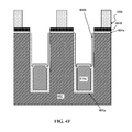
- FIG. 4A-4G are a sequence of cross-sectional schematic diagrams illustrating a method of fabrication of a trench power MOSFET according to one embodiment of the present disclosure.
- Embodiments of the present disclosure present a self-aligned contact for trench power MOSFETs and methods of fabricating the same.
- FIGS. 1A-1Q is a sequence of cross-sectional schematic diagrams illustrating a method of fabrication of the device according to one embodiment of the present disclosure.
- the process uses a semiconductor substrate 102 as a starting material.
- the substrate 102 may be divided into multiple die.
- Each die may include an active cell area and a gate pickup/contact area at the periphery of a die.
- the active cell area contains multiple cells (e.g., MOSFET cells) having the same or similar structure.
- a hard mask layer 104 of a suitable material, such as oxide or nitride, can be formed on top of the semiconductor substrate 102 .
- the thickness of the hard mask 104 may be about 0.15 ⁇ m to about 1.00 ⁇ m.
- a photoresist (not shown) is formed on the hard mask 104 and patterned to define patterns for the gate trenches. Portions of the hard mask 104 exposed to an etchant through openings in the photoresist are etched away and the etching stops at the silicon surface leaving an opening that will be used to mask the etching of trenches. Thereafter, gate trenches 106 are formed on the active cell area by etching away the substrate underneath the trench openings as shown in FIG. 1A .
- a thin sacrificial oxide grows on all of the silicon surfaces to oxidize silicon portions that were damaged during the etching.
- a wet etch with hydrofluoric acid (HF) is performed to remove the sacrificial oxide and etch back the width of the hardmask 104 on top of the silicon to leave remaining portions that are of the desired size and shape for the future contact as shown in FIG. 1B .
- HF hydrofluoric acid
- an oxidation is performed to grow gate oxide 108 by oxidizing the silicon.
- the thickness of the gate oxide 108 is about 150-1000 ⁇ and preferably 150-600 ⁇ .
- conductive material 110 such as polysilicon
- CMP chemical mechanical polishing
- the conductive material 110 is then etched to the desired recess below the mesa between the trenches 106 .
- a poly re-oxidation is performed to form a desired thickness of oxide 111 over the conductive material 110 as shown in FIG. 1D .
- a body implant to form a plurality of body regions 112 a is carried out with or without a body mask by implanting dopants into the top portions of the semiconductor substrate 102 .
- heat is applied to activate dopant atoms and drive dopant diffusion to form a body region 112 (e.g., a p-type or n-type body region depending on the type of dopants implanted) in the substrate 102 .
- a plurality of source regions 114 are formed by applying a source mask to carry out a source dopant implant.
- the processes for the body implant and the source implant may be identical to corresponding stages of the current standard trench MOSFET process.
- FIG. 1H shows a layer of nitride 116 is deposited over the top of the structure of FIG. 1G (including the hard mask structure 104 ) by low pressure chemical vapor deposition (LPCVD).
- the thickness of the nitride 116 is equal or larger than the width of the exposed mesa.
- the nitride 116 may be in a thickness of about 0.08 ⁇ m to about 0.50 ⁇ m.
- a thin photoresist layer 118 may be coated on top of the structure of FIG. 1H without exposing it and/or without using it as a mask.
- the photoresist layer 118 here is used as a space holder.
- a blanket etch of the photoresist layer 118 is performed leaving exposed elevated portions of the nitride 116 and leaving photoresist 118 in the recesses between the elevated portions of the nitride 116 as shown in FIG. 1J .
- a nitride etch of the top portion of the nitride 116 as shown in FIG. 1K is performed with a process that preferentially etches the nitride exposing the oxide hardmask 104 and leaving the photoresist behind.
- the photoresist layer 118 is removed by wet chemical solvent or dry plasma.
- an oxide layer 118 a (e.g., high density plasma (HDP) oxide) may be used instead of a photoresist layer.
- An oxide may be deposited over the structure of FIG. 1H by HDP deposition.
- An oxide-selective CMP may then be performed to remove the HDP oxide down to the surface of the elevated portions of the nitride 116 .
- a nitride etch back is performed to etch portions of nitride 116 exposing the oxide hardmask 104 and leaving the HDP oxide behind.
- FIG. 1L-1 shows the structure at the stage corresponding to FIG. 1L when replacing the photoresist layer with HDP oxide.
- a low temperature oxide (LTO) layer 120 and a borophosphosilicate glass (BPSG) layer 122 are deposited over the structure of FIG. 1L (as shown in FIG. 1M ) or FIG. 1L-1 .
- LTO low temperature oxide
- BPSG borophosphosilicate glass
- a contact mask (not shown) is applied to protect other portions of the device (e.g., gate pickup area) and expose only portions of the active cell area. It is noted that another contact mask may be needed for gate pickup area.
- an oxide etch is performed though openings in the contact mask. The oxide etch may be stopped at the mesa surface by using an anisotropic (e.g., plasma) oxide etch of high selectivity to nitride and silicon. This etch removes the remaining oxide hardmask 104 (and the HDP oxide if using HDP oxide instead of photoresist 118 ) and leaves nitride 116 behind.
- the process can be done as long as layer 116 material is resistant to the process that etches the hard mask material 104 .
- the oxide and nitride can be reversed.
- the hardmask 104 can be made of nitride and the layer 116 can be made of oxide.
- a second source implant may be optionally performed.
- the source implant may be done with an angled implant and drive-in process.
- a contact etch process etches the upper portions of the substrate 102 through the openings in the remaining nitride 116 as shown in FIG. 1P to create contact openings 124 .
- a barrier metal layer 126 is lined on the sidewalls and bottom of the contact openings followed by the deposition of a conductive material, e.g., Tungsten, in the contact openings 124 forming the conductive plugs 128 .
- a layer of metal 130 e.g., aluminum
- Standard processing may then complete the formation of trench MOSFET devices.
- the device of FIG. 1Q has nitride 116 on top of the gate poly 110 and over portions of the mesa between the contacts 128 .
- the nitride 116 acts as a good barrier to diffusion of moisture, mobile ions, etc.
- FIGS. 2A-2I is a sequence of cross-sectional schematic diagrams illustrating a method of fabrication of a device with non-uniform thickness of oxide in trenches according to one embodiment of the present disclosure. Similar to the first embodiment, the process starts with a semiconductor substrate 202 as a starting material. A hard mask layer 204 of a suitable material, such as oxide or nitride, can be formed on top of the semiconductor substrate 202 . A photoresist (not shown) is formed on the hard mask 204 and patterned to define patterns for the gate trenches.
- a suitable material such as oxide or nitride
- Portions of the hard mask 204 exposed to an etchant through openings in the photoresist are etched away and the etching stops at the silicon surface leaving an opening that will be used to mask the etching of trenches. Thereafter, gate trenches 206 are formed on the active cell area by etching away the substrate underneath the trench openings as shown in FIG. 2A .
- a thin sacrificial oxide (not shown) is removed after it grows on all of the silicon surfaces to oxidize silicon portions that were damaged during the etching. Unlike the first embodiment, the width of the hardmask 204 is not etched back to the width of the contact into silicon during this step.
- a liner oxide 208 a grows on the sidewalls of the gate trenches 206 by, e.g., CVD.
- the thickness of the liner oxide 208 a is about 2 to 5 times of the thickness of the gate oxide 108 in the first embodiment.
- the thickness of the liner oxide 208 a is in a range of 0.06 ⁇ m to about 0.30 ⁇ m.
- conductive material 210 a such as polysilicon, is deposited into the trenches and over the semiconductor substrate followed by a chemical mechanical polishing (CMP) to remove polysilicon back to top of the hardmask 204 .
- CMP chemical mechanical polishing
- the conductive material 210 a is then etched to a desired depth in the trenches 206 as shown in FIG. 2D .
- a wet etch with hydrofluoric acid (HF) is performed to remove the liner oxide 208 a and the hard mask 204 to a desired width for contacts.
- a gate oxide 208 b is grown on the conductive material 210 a and along trench sidewalls above the conductive material 210 a as shown in FIG. 2F .
- the thickness of the gate oxide 208 b is thinner than the liner oxide 208 a .
- the thickness of the gate oxide 208 b is in a range of 0.015 ⁇ m to about 0.060 ⁇ m.
- conductive material 210 b such as polysilicon, is deposited into the upper portion of the trenches and etched to a desired recess below the mesa between the trenches 206 .
- a poly re-oxidation is performed to form a desired thickness of oxide 211 over the conductive material 210 b as shown in FIG. 2G .
- a body implant into area 212 a is carried out to form a plurality of body regions 212 a followed by a body drive to form a body region 212 (e.g., a p-type or n-type body region depending on the type of dopants implanted) in the substrate 202 .
- a plurality of source regions 214 are formed by applying a source mask to carry out a source dopant implant. Thereafter, the processes identical to the processes of FIGS. 1H-1Q are applied to form contacts by using the hardmask 204 as space holders.
- the device according to this embodiment of the present disclosure also has nitride on top of the gate poly 210 b and over portions of the mesa between the contacts as in the first embodiment to form self-aligned contact devices.
- the device according to this embodiment has two conductive materials 210 a and 210 b in each gate trench and has non-uniform thickness of oxide in the trench. It is noted that while there is insulating material between the conductive material 210 a and 210 b , the conductive material 210 a and 210 b may be electrically connected together or respectively to source and gate electrodes for device performance that is different from that of the structure in the first embodiment
- FIGS. 3A-3U is a sequence of cross-sectional schematic diagrams illustrating a method of fabrication of the device according to one embodiment of the present disclosure.
- the process uses a semiconductor substrate 302 as a starting material.
- a hard mask layer 304 can be formed on top of the substrate 302 by forming a thin oxide layer 304 a on the substrate 302 by deposition or thermal oxidation, followed by a nitride layer 304 b on top of the thin oxide layer 304 a .
- the thickness of the silicon oxide layer ranges from about 100 ⁇ to 500 ⁇ and is preferably about 200 ⁇ .
- the thickness of the nitride layer ranges from 1500 ⁇ to 4000 ⁇ .
- Another oxide layer 304 c may be disposed on top of the nitride layer 304 b to form the hard mask with an oxide/nitride/oxide stack.
- the thickness of the oxide layer 304 c ranges from 1000 ⁇ to 7000 ⁇ .
- a photoresist (not shown) is formed on the hard mask 304 and patterned to define patterns for the gate trenches. Portions of the hard mask 304 exposed to an etchant through openings in the photoresist are etched away and the etching stops at the silicon surface leaving an opening that will be used to mask the etching of trenches. Thereafter, gate trenches 306 are formed on the active cell area by etching away the substrate underneath the trench openings as shown in FIG. 3A .
- a sacrificial oxide grows on all of the silicon surfaces to oxidize silicon portions that were damaged during the etching.
- a wet etch with hydrofluoric acid (HF) is performed to remove the sacrificial oxide and etch back the width of the oxide layer 304 c on top of the nitride layer 304 b to leave opening of the desired size for the future contact as shown in FIG. 3B .
- HF hydrofluoric acid
- an oxidation is performed to grow gate oxide 308 by oxidizing the silicon.
- the thickness of the gate oxide 308 is about 150-1000 ⁇ and preferably 150-600 ⁇ .
- conductive material 310 such as polysilicon, is deposited into the trenches and over the semiconductor substrate followed by a chemical mechanical polishing (CMP) to remove polysilicon back to top of the oxide layer 304 c .
- CMP chemical mechanical polishing
- the conductive material 310 is then etched to the desired recess below the mesa between the trenches 306 as shown in FIG. 3D .
- An oxidation on the conductive material 310 is carried out to form a thick layer 311 of oxidation.
- the thick oxide layer 311 is thicker than the oxide layer 111 or 211 in the first and second embodiments.
- the thick layer 311 is about 3 to 6 times of the thickness of the gate oxide 308 .
- the thickness of the thick oxide layer 311 is in a range of 0.05 ⁇ m to about 0.30 ⁇ m.
- an etch is performed to remove the exposed nitride 304 b .
- a body implant to form a plurality of body regions 312 a is carried out with a body mask by implanting dopants into the top portions of the semiconductor substrate 302 .
- heat is applied to activate dopant atoms and drive dopant diffusion to form a body region 312 (e.g., a p-type or n-type body region depending on the type of dopants implanted) in the substrate 302 .
- the body drive with oxygen may grow more oxidation on the exposed mesa. This oxidation could be also carried out at source drive.
- a plurality of source regions 314 are formed by applying a source mask to carry out a source dopant implant.
- FIG. 3J shows a layer of nitride 316 is deposited over the top of the structure of FIG. 3I by low pressure chemical vapor deposition (LPCVD).
- the thickness of the nitride 316 is equal or larger than the width of the exposed mesa.
- the nitride 316 may be in a thickness range from about [0.080 ⁇ m to about [0.500 ⁇ m.
- a thin photoresist layer 318 may be coated on top of the structure of FIG. 3J without exposing it or without patterning it to form a mask. Instead, the photoresist layer 318 is used as a space holder. A blanket etch of the photoresist layer 318 is performed leaving exposed elevated portions of the nitride 316 and leaving photoresist 318 in recesses between the elevated portions of the nitride 316 as shown in FIG. 3L . A nitride etch of the top portion of the nitride 316 as shown in FIG.
- 3M is performed with a process that preferentially etches the nitride exposing the oxide hardmask 304 c and leaving the photoresist behind.
- the photoresist layer 318 is removed by wet chemical solvent or dry plasma.
- the photoresist layer 318 may be replaced by an oxide layer 318 a (e.g., HDP oxide).
- An oxide may be deposited over the structure of FIG. 3J by HDP deposition.
- An oxide-selective CMP is performed to remove the HDP oxide and stop at the surface of the elevated portions of the nitride 316 .
- a nitride etch back is performed to etch portions of nitride 316 exposing the oxide hardmask 304 c and leaving the HDP oxide behind.
- FIG. 3N-1 shows the structure at the stage corresponding to FIG. 3N when replacing the photoresist layer with HDP oxide.
- a LTO layer 320 and a BPSG layer 322 are deposited over the structure of FIG. 3N (as shown in FIG. 3O ) or FIG. 3N-1 .
- a contact mask (not shown) is applied to protect other portions of the device (e.g., gate pickup area) and expose only portions of the active cell area. It is noted that another contact mask may be needed for gate pickup area.
- an oxide etch is performed with the contact mask and stops on the nitride 304 b over the mesa. This etch removes the remaining oxide hardmask 304 c (and the HDP oxide if using HDP oxide instead of photoresist 318 ) and leaves nitride 316 and 304 b over the mesa behind.
- a second source implant may be optionally performed when the source implant is angled or driven. Then a contact etch etches through the openings in the remaining nitride (including the nitride 304 b above the mesa) as shown in FIG. 3R to create contact openings 324 .
- a thin thermal oxide 340 is grown along the contact trench 324 to protect the silicon surface during the nitride strip in the next step. In some embodiments, the thickness of the thin oxide 340 is about 150 ⁇ .
- a nitride strip is carried out in FIG. 3T followed by removing the thin oxide 340 inside the contact trench 324 with a buffered oxide etch (BOE) or a wet etch with HF.
- BOE buffered oxide etch
- a barrier metal layer 326 is lined on the sidewalls and bottom of the contact openings 324 followed by the deposition of a conductive material, e.g., Tungsten, in the contact openings 324 forming the conductive plugs 328 .
- a layer of metal 330 e.g., aluminum is deposited on the top of the structure. The wafer is then followed the rest of standard trench MOSFET steps to complete the processing.
- the device of FIG. 3U has no nitride left behind.
- the device has oxide on top of the mesa and between the contacts 328 and has thicker oxide rounded corners of the mesa. It is noted that the thicker oxide at mesa corners may reduce breakdown voltage.
- FIGS. 4A-4I is a sequence of a sequence of cross-sectional schematic diagrams illustrating a method of fabrication of such a device according to one embodiment of the present disclosure.
- the process starts with a semiconductor substrate 402 as a stating material.
- a hard mask layer 404 can be formed on top of the substrate 402 by forming a thin oxide layer 404 a on the substrate 402 by deposition or thermal oxidation, followed by a nitride layer 404 b on top of the thin oxide layer 404 a .
- the thickness of the silicon oxide layer ranges from about 100 ⁇ to 500 ⁇ and is preferably about 200 ⁇ . In some embodiments, the thickness of the nitride layer ranges from 1500 ⁇ to 4000 ⁇ .
- Another oxide layer 404 c may be disposed on top of the nitride layer 404 b to form the hard mask with an oxide/nitride/oxide stack. In some embodiments, the thickness of the oxide layer 404 c ranges from 1000 ⁇ to 7000 ⁇ .
- a photoresist (not shown) is formed on the hard mask 404 and patterned to define patterns for the gate trenches.
- gate trenches 406 are formed on the active cell area by etching away the substrate underneath the trench openings as shown in FIG. 4A .
- a thin sacrificial oxide (not shown) is removed after it grows on all of the silicon surfaces to oxidize silicon portions that were damaged during the etching.
- the width of the hardmask 404 is not etched back during this step.
- a liner oxide 408 a grows on the sidewalls of the gate trenches 406 by, e.g., CVD.
- the thickness of the liner oxide 408 a is about 2 to 5 times of the thickness of the gate oxide 108 in the first embodiment.
- the thickness of the liner oxide 408 a is in a range of 0.060 ⁇ m to about 0.300 ⁇ m.
- conductive material 410 a such as polysilicon, is deposited into the trenches and over the semiconductor substrate followed by a chemical mechanical polishing (CMP) to remove polysilicon back to top of the hardmask 404 .
- CMP chemical mechanical polishing
- the conductive material 410 a is then etched to a desired depth in the trenches 406 as shown in FIG. 4D .
- a wet etch with hydrofluoric acid (HF) is performed to remove the liner oxide 408 to a desired depth and etch back the width of the oxide layer 404 c on top of the nitride layer 404 b to leave remaining of the desired size for the future contact as shown in FIG. 4E .
- a gate oxide 408 b is grown on the conductive material 410 a and along trench sidewalls above the conductive material 410 a as shown in FIG. 4F .
- the thickness of the gate oxide 408 b is thinner than the liner oxide 408 a .
- the thickness of the gate oxide 408 b is in a range of 0.015 ⁇ m to about 0.060 ⁇ m.
- conductive material 410 b such as polysilicon, is deposited into the upper portion of the trenches followed by etching the conductive material to the desired recess below the mesa between the trenches 406 .
- An oxidation on the conductive material 410 a is carried out to form a thick layer 411 of oxidation.
- the thick oxide layer 411 is thicker than the oxide layer 111 or 211 in the first and second embodiments.
- the thick layer 411 is about 3 to 6 times of the thickness of the gate oxide 408 .
- the thickness of the thick oxide layer 411 is in a range of 0.050 ⁇ m to about 0.300 ⁇ m.
- aspects of the present disclosure allow for fabrication of self-aligned contacts without having to form spacers below the surface of the silicon substrate to do self-aligned contact. This avoids the loss of significant amounts of original semiconductor substrate material in the mesa region when using spacers below the surface. Aspects of the present disclosure also reduce the number of process steps used to fabricate the contacts by forming space holders for future contact positions in the semiconductor substrate using part of the hard mask for trench definition.
Abstract
Embodiments of the present disclosure provide a self-aligned contact for a trench power MOSFET device. The device has a layer of nitride provided over the conductive material in the gate trenches and over portions of mesas between every two adjacent contact structures. Alternatively, the device has an oxide layer over the conductive material in the gate trenches and over portions of mesas between every two adjacent contact structures. It is emphasized that this abstract is provided to comply with rules requiring an abstract that will allow a searcher or other reader to quickly ascertain the subject matter of the technical disclosure. It is submitted with the understanding that it will not be used to interpret or limit the scope or meaning of the claims.
Description
This present disclosure relates generally to semiconductor power devices, and more particularly to a self-aligned trench MOSFET and methods of manufacturing such devices.
Power metal oxide semiconductor field effect transistors (MOSFETs) are commonly used power devices due to their low gate drive power, fast switching speed and superior paralleling capability. A trench gate of a MOSFET device typically includes a trench extending into a semiconductor substrate from the source to the drain and having sidewalls and a floor that are each lined with a layer of an insulator such as thermally grown silicon dioxide. The lined trench is filled with doped polysilicon that acts as the gate. The structure of the trench gate allows less constricted current flow and, consequently, provides lower values of specific on-resistance. Furthermore, the trench gate makes possible a decreased cell pitch in a MOSFET channel extending along the sidewalls of the trench from the bottom of the source across the body of the transistor to the drain below. Channel density is thereby increased, which reduces the channel's contribution to on-resistance.
A high density trench MOSFET device also includes a contact trench in a mesa region between adjacent gate trenches to provide contact to source and body regions. Conventional processes for manufacturing trench MOSFET devices have used separate mask processes to define the gate and contact trenches. However, a mask overlay issue occurs when forming a vertical MOSFET structure because a well-controlled spacing between the gate trench and nearby contact trench is required for high density MOSFET devices, which have increasingly smaller dimensions. Schemes based on self-alignment processes have been proposed to solve this mask overlay issue. However, these proposed schemes use spacers formed below the surface of the semiconductor substrate to create a self-aligned contact trench. As a result, a lot of original silicon is lost in the mesa regions between the contract trenches. In addition, the proposed schemes use many process steps and are complicated to implement.
It is within this context that embodiments of the present invention arise.
Objects and advantages of the invention will become apparent upon reading the following detailed description and upon reference to the accompanying drawings in which:
In the following Detailed Description, reference is made to the accompanying drawings, which form a part hereof, and in which is shown by way of illustration specific embodiments in which the invention may be practiced. In this regard, directional terminology, such as “top,” “bottom,” “front,” “back,” “leading,” “trailing,” etc., is used with reference to the orientation of the figure(s) being described. Because components of embodiments of the present invention can be positioned in a number of different orientations, the directional terminology is used for purposes of illustration and is in no way limiting. It is to be understood that other embodiments may be utilized and structural or logical changes may be made without departing from the scope of the present invention. The following detailed description, therefore, is not to be taken in a limiting sense, and the scope of the present invention is defined by the appended claims.
Embodiments of the present disclosure present a self-aligned contact for trench power MOSFETs and methods of fabricating the same.
First Embodiment
A hard mask layer 104 of a suitable material, such as oxide or nitride, can be formed on top of the semiconductor substrate 102. The thickness of the hard mask 104 may be about 0.15 μm to about 1.00 μm. A photoresist (not shown) is formed on the hard mask 104 and patterned to define patterns for the gate trenches. Portions of the hard mask 104 exposed to an etchant through openings in the photoresist are etched away and the etching stops at the silicon surface leaving an opening that will be used to mask the etching of trenches. Thereafter, gate trenches 106 are formed on the active cell area by etching away the substrate underneath the trench openings as shown in FIG. 1A .
A thin sacrificial oxide (not shown) grows on all of the silicon surfaces to oxidize silicon portions that were damaged during the etching. A wet etch with hydrofluoric acid (HF) is performed to remove the sacrificial oxide and etch back the width of the hardmask 104 on top of the silicon to leave remaining portions that are of the desired size and shape for the future contact as shown in FIG. 1B . In FIG. 1C , an oxidation is performed to grow gate oxide 108 by oxidizing the silicon. In some embodiments, the thickness of the gate oxide 108 is about 150-1000 Å and preferably 150-600 Å.
Next, conductive material 110, such as polysilicon, is deposited into the trenches and over the semiconductor substrate followed by a chemical mechanical polishing (CMP) to remove polysilicon back to top of the hardmask 104. The conductive material 110 is then etched to the desired recess below the mesa between the trenches 106. A poly re-oxidation is performed to form a desired thickness of oxide 111 over the conductive material 110 as shown in FIG. 1D .
As shown in FIG. 1E , a body implant to form a plurality of body regions 112 a is carried out with or without a body mask by implanting dopants into the top portions of the semiconductor substrate 102. In FIG. 1F , heat is applied to activate dopant atoms and drive dopant diffusion to form a body region 112 (e.g., a p-type or n-type body region depending on the type of dopants implanted) in the substrate 102. In FIG. 1G , a plurality of source regions 114 are formed by applying a source mask to carry out a source dopant implant. The processes for the body implant and the source implant may be identical to corresponding stages of the current standard trench MOSFET process.
In FIG. 1I , a thin photoresist layer 118 may be coated on top of the structure of FIG. 1H without exposing it and/or without using it as a mask. The photoresist layer 118 here is used as a space holder. A blanket etch of the photoresist layer 118 is performed leaving exposed elevated portions of the nitride 116 and leaving photoresist 118 in the recesses between the elevated portions of the nitride 116 as shown in FIG. 1J . A nitride etch of the top portion of the nitride 116 as shown in FIG. 1K is performed with a process that preferentially etches the nitride exposing the oxide hardmask 104 and leaving the photoresist behind. In FIG. 1L , the photoresist layer 118 is removed by wet chemical solvent or dry plasma.
Alternatively for the processes of FIGS. 1I-1L , an oxide layer 118 a (e.g., high density plasma (HDP) oxide) may be used instead of a photoresist layer. An oxide may be deposited over the structure of FIG. 1H by HDP deposition. An oxide-selective CMP may then be performed to remove the HDP oxide down to the surface of the elevated portions of the nitride 116. A nitride etch back is performed to etch portions of nitride 116 exposing the oxide hardmask 104 and leaving the HDP oxide behind. FIG. 1L-1 shows the structure at the stage corresponding to FIG. 1L when replacing the photoresist layer with HDP oxide.
Next, a low temperature oxide (LTO) layer 120 and a borophosphosilicate glass (BPSG) layer 122 are deposited over the structure of FIG. 1L (as shown in FIG. 1M ) or FIG. 1L-1 .
A contact mask (not shown) is applied to protect other portions of the device (e.g., gate pickup area) and expose only portions of the active cell area. It is noted that another contact mask may be needed for gate pickup area. In FIG. 1N , an oxide etch is performed though openings in the contact mask. The oxide etch may be stopped at the mesa surface by using an anisotropic (e.g., plasma) oxide etch of high selectivity to nitride and silicon. This etch removes the remaining oxide hardmask 104 (and the HDP oxide if using HDP oxide instead of photoresist 118) and leaves nitride 116 behind. It is noted that the process can be done as long as layer 116 material is resistant to the process that etches the hard mask material 104. Thus, the oxide and nitride can be reversed. In other words, the hardmask 104 can be made of nitride and the layer 116 can be made of oxide.
As shown in FIG. 1O , a second source implant may be optionally performed. The source implant may be done with an angled implant and drive-in process. Then a contact etch process etches the upper portions of the substrate 102 through the openings in the remaining nitride 116 as shown in FIG. 1P to create contact openings 124. In FIG. 1Q , a barrier metal layer 126 is lined on the sidewalls and bottom of the contact openings followed by the deposition of a conductive material, e.g., Tungsten, in the contact openings 124 forming the conductive plugs 128. Following that, a layer of metal 130 (e.g., aluminum) is deposited on the top of the structure. Standard processing may then complete the formation of trench MOSFET devices.
The device of FIG. 1Q according to this embodiment of the present disclosure has nitride 116 on top of the gate poly 110 and over portions of the mesa between the contacts 128. The nitride 116 acts as a good barrier to diffusion of moisture, mobile ions, etc.
Second Embodiment
In FIG. 2B , a thin sacrificial oxide (not shown) is removed after it grows on all of the silicon surfaces to oxidize silicon portions that were damaged during the etching. Unlike the first embodiment, the width of the hardmask 204 is not etched back to the width of the contact into silicon during this step. In FIG. 2C , a liner oxide 208 a grows on the sidewalls of the gate trenches 206 by, e.g., CVD. The thickness of the liner oxide 208 a is about 2 to 5 times of the thickness of the gate oxide 108 in the first embodiment. By way of the example and not by way of limitation, the thickness of the liner oxide 208 a is in a range of 0.06 μm to about 0.30 μm.
Next, conductive material 210 a, such as polysilicon, is deposited into the trenches and over the semiconductor substrate followed by a chemical mechanical polishing (CMP) to remove polysilicon back to top of the hardmask 204. The conductive material 210 a is then etched to a desired depth in the trenches 206 as shown in FIG. 2D .
In FIG. 2E , a wet etch with hydrofluoric acid (HF) is performed to remove the liner oxide 208 a and the hard mask 204 to a desired width for contacts. A gate oxide 208 b is grown on the conductive material 210 a and along trench sidewalls above the conductive material 210 a as shown in FIG. 2F . The thickness of the gate oxide 208 b is thinner than the liner oxide 208 a. In some embodiments, the thickness of the gate oxide 208 b is in a range of 0.015 μm to about 0.060 μm.
Next, conductive material 210 b, such as polysilicon, is deposited into the upper portion of the trenches and etched to a desired recess below the mesa between the trenches 206. A poly re-oxidation is performed to form a desired thickness of oxide 211 over the conductive material 210 b as shown in FIG. 2G .
As shown in FIG. 2G and FIG. 2H , a body implant into area 212 a is carried out to form a plurality of body regions 212 a followed by a body drive to form a body region 212 (e.g., a p-type or n-type body region depending on the type of dopants implanted) in the substrate 202. In FIG. 2I , a plurality of source regions 214 are formed by applying a source mask to carry out a source dopant implant. Thereafter, the processes identical to the processes of FIGS. 1H-1Q are applied to form contacts by using the hardmask 204 as space holders.
The device according to this embodiment of the present disclosure also has nitride on top of the gate poly 210 b and over portions of the mesa between the contacts as in the first embodiment to form self-aligned contact devices. The device according to this embodiment has two conductive materials 210 a and 210 b in each gate trench and has non-uniform thickness of oxide in the trench. It is noted that while there is insulating material between the conductive material 210 a and 210 b, the conductive material 210 a and 210 b may be electrically connected together or respectively to source and gate electrodes for device performance that is different from that of the structure in the first embodiment
Third Embodiment
A sacrificial oxide (not shown) grows on all of the silicon surfaces to oxidize silicon portions that were damaged during the etching. A wet etch with hydrofluoric acid (HF) is performed to remove the sacrificial oxide and etch back the width of the oxide layer 304 c on top of the nitride layer 304 b to leave opening of the desired size for the future contact as shown in FIG. 3B . In FIG. 3C , an oxidation is performed to grow gate oxide 308 by oxidizing the silicon. In some embodiments, the thickness of the gate oxide 308 is about 150-1000 Å and preferably 150-600 Å.
Next, conductive material 310, such as polysilicon, is deposited into the trenches and over the semiconductor substrate followed by a chemical mechanical polishing (CMP) to remove polysilicon back to top of the oxide layer 304 c. The conductive material 310 is then etched to the desired recess below the mesa between the trenches 306 as shown in FIG. 3D .
An oxidation on the conductive material 310 is carried out to form a thick layer 311 of oxidation. It is noted that the thick oxide layer 311 is thicker than the oxide layer 111 or 211 in the first and second embodiments. In some embodiments, the thick layer 311 is about 3 to 6 times of the thickness of the gate oxide 308. By way of the example and not by way of limitation, the thickness of the thick oxide layer 311 is in a range of 0.05 μm to about 0.30 μm. It is noted that when the conductive material 310 is recessed below mesa to a certain amount, mesa will get oxidation from the side and also under the nitride 304 b rounding the mesa corner and bending up the nitride 304 b as shown in FIG. 3E . This configuration is sometimes referred to as a “bird's beak”.
In FIG. 3F , an etch, either dry etch or wet etch, is performed to remove the exposed nitride 304 b. As shown in FIG. 3G , a body implant to form a plurality of body regions 312 a is carried out with a body mask by implanting dopants into the top portions of the semiconductor substrate 302. In FIG. 3H , heat is applied to activate dopant atoms and drive dopant diffusion to form a body region 312 (e.g., a p-type or n-type body region depending on the type of dopants implanted) in the substrate 302. It is noted that the body drive with oxygen may grow more oxidation on the exposed mesa. This oxidation could be also carried out at source drive. In FIG. 3I , a plurality of source regions 314 are formed by applying a source mask to carry out a source dopant implant.
In FIG. 3K , a thin photoresist layer 318 may be coated on top of the structure of FIG. 3J without exposing it or without patterning it to form a mask. Instead, the photoresist layer 318 is used as a space holder. A blanket etch of the photoresist layer 318 is performed leaving exposed elevated portions of the nitride 316 and leaving photoresist 318 in recesses between the elevated portions of the nitride 316 as shown in FIG. 3L . A nitride etch of the top portion of the nitride 316 as shown in FIG. 3M is performed with a process that preferentially etches the nitride exposing the oxide hardmask 304 c and leaving the photoresist behind. In FIG. 3N , the photoresist layer 318 is removed by wet chemical solvent or dry plasma.
As discussed above in connection with the first embodiment, the photoresist layer 318 may be replaced by an oxide layer 318 a (e.g., HDP oxide). An oxide may be deposited over the structure of FIG. 3J by HDP deposition. An oxide-selective CMP is performed to remove the HDP oxide and stop at the surface of the elevated portions of the nitride 316. A nitride etch back is performed to etch portions of nitride 316 exposing the oxide hardmask 304 c and leaving the HDP oxide behind. FIG. 3N-1 shows the structure at the stage corresponding to FIG. 3N when replacing the photoresist layer with HDP oxide.
Next, a LTO layer 320 and a BPSG layer 322 are deposited over the structure of FIG. 3N (as shown in FIG. 3O ) or FIG. 3N-1 . A contact mask (not shown) is applied to protect other portions of the device (e.g., gate pickup area) and expose only portions of the active cell area. It is noted that another contact mask may be needed for gate pickup area. In FIG. 3P , an oxide etch is performed with the contact mask and stops on the nitride 304 b over the mesa. This etch removes the remaining oxide hardmask 304 c (and the HDP oxide if using HDP oxide instead of photoresist 318) and leaves nitride 316 and 304 b over the mesa behind.
As shown in FIG. 3Q , a second source implant may be optionally performed when the source implant is angled or driven. Then a contact etch etches through the openings in the remaining nitride (including the nitride 304 b above the mesa) as shown in FIG. 3R to create contact openings 324. In FIG. 3S , a thin thermal oxide 340 is grown along the contact trench 324 to protect the silicon surface during the nitride strip in the next step. In some embodiments, the thickness of the thin oxide 340 is about 150 Å. A nitride strip is carried out in FIG. 3T followed by removing the thin oxide 340 inside the contact trench 324 with a buffered oxide etch (BOE) or a wet etch with HF.
Next, a barrier metal layer 326 is lined on the sidewalls and bottom of the contact openings 324 followed by the deposition of a conductive material, e.g., Tungsten, in the contact openings 324 forming the conductive plugs 328. Following that, a layer of metal 330 (e.g., aluminum) is deposited on the top of the structure. The wafer is then followed the rest of standard trench MOSFET steps to complete the processing.
The device of FIG. 3U according to this embodiment of the present disclosure has no nitride left behind. In addition, the device has oxide on top of the mesa and between the contacts 328 and has thicker oxide rounded corners of the mesa. It is noted that the thicker oxide at mesa corners may reduce breakdown voltage.
Fourth Embodiment
It is noted that another embodiment of the present disclosure may provide a device and a method of fabrication of a device having non-uniform thickness of oxide in two-poly gate trenches similar to the second embodiment with an ONO stack as hardmask. FIGS. 4A-4I is a sequence of a sequence of cross-sectional schematic diagrams illustrating a method of fabrication of such a device according to one embodiment of the present disclosure. the process starts with a semiconductor substrate 402 as a stating material. A hard mask layer 404 can be formed on top of the substrate 402 by forming a thin oxide layer 404 a on the substrate 402 by deposition or thermal oxidation, followed by a nitride layer 404 b on top of the thin oxide layer 404 a. In some embodiments, the thickness of the silicon oxide layer ranges from about 100 Å to 500 Å and is preferably about 200 Å. In some embodiments, the thickness of the nitride layer ranges from 1500 Å to 4000 Å. Another oxide layer 404 c may be disposed on top of the nitride layer 404 b to form the hard mask with an oxide/nitride/oxide stack. In some embodiments, the thickness of the oxide layer 404 c ranges from 1000 Å to 7000 Å. A photoresist (not shown) is formed on the hard mask 404 and patterned to define patterns for the gate trenches. Portions of the hard mask 404 exposed to an etchant through openings in the photoresist are etched away and the etching stops at the silicon surface leaving an opening that will be used to mask the etching of trenches. Thereafter, gate trenches 406 are formed on the active cell area by etching away the substrate underneath the trench openings as shown in FIG. 4A .
In FIG. 4B , a thin sacrificial oxide (not shown) is removed after it grows on all of the silicon surfaces to oxidize silicon portions that were damaged during the etching. The width of the hardmask 404 is not etched back during this step. In FIG. 4C , a liner oxide 408 a grows on the sidewalls of the gate trenches 406 by, e.g., CVD. The thickness of the liner oxide 408 a is about 2 to 5 times of the thickness of the gate oxide 108 in the first embodiment. By way of the example and not by way of limitation, the thickness of the liner oxide 408 a is in a range of 0.060 μm to about 0.300 μm.
Next, conductive material 410 a, such as polysilicon, is deposited into the trenches and over the semiconductor substrate followed by a chemical mechanical polishing (CMP) to remove polysilicon back to top of the hardmask 404. The conductive material 410 a is then etched to a desired depth in the trenches 406 as shown in FIG. 4D .
In FIG. 4E , a wet etch with hydrofluoric acid (HF) is performed to remove the liner oxide 408 to a desired depth and etch back the width of the oxide layer 404 c on top of the nitride layer 404 b to leave remaining of the desired size for the future contact as shown in FIG. 4E . A gate oxide 408 b is grown on the conductive material 410 a and along trench sidewalls above the conductive material 410 a as shown in FIG. 4F . The thickness of the gate oxide 408 b is thinner than the liner oxide 408 a. In some embodiments, the thickness of the gate oxide 408 b is in a range of 0.015 μm to about 0.060 μm.
Next, conductive material 410 b, such as polysilicon, is deposited into the upper portion of the trenches followed by etching the conductive material to the desired recess below the mesa between the trenches 406. An oxidation on the conductive material 410 a is carried out to form a thick layer 411 of oxidation. It is noted that the thick oxide layer 411 is thicker than the oxide layer 111 or 211 in the first and second embodiments. In some embodiments, the thick layer 411 is about 3 to 6 times of the thickness of the gate oxide 408. By way of the example and not by way of limitation, the thickness of the thick oxide layer 411 is in a range of 0.050 μm to about 0.300 μm. It is noted that when the conductive material 410 is recessed below mesa to a certain amount, mesa will get oxidation from the side and also under the nitride 404 b rounding the mesa corner and bending up the nitride 404 b as shown in FIG. 4G . Thereafter, the processes identical to the processes of FIGS. 3F-3U are applied to form contacts.
Aspects of the present disclosure allow for fabrication of self-aligned contacts without having to form spacers below the surface of the silicon substrate to do self-aligned contact. This avoids the loss of significant amounts of original semiconductor substrate material in the mesa region when using spacers below the surface. Aspects of the present disclosure also reduce the number of process steps used to fabricate the contacts by forming space holders for future contact positions in the semiconductor substrate using part of the hard mask for trench definition.
While the above is a complete description of the preferred embodiments of the present invention, it is possible to use various alternatives, modifications, and equivalents. Therefore, the scope of the present invention should be determined not with reference to the above description but should, instead, be determined with reference to the appended claims, along with their full scope of equivalents. Any feature, whether preferred or not, may be combined with any other feature, whether preferred or not. In the claims that follow, the indefinite article “A” or “An” refers to a quantity of one or more of the item following the article, except where expressly stated otherwise. The appended claims are not to be interpreted as including means-plus-function limitations, unless such a limitation is explicitly recited in a given claim using the phrase “means for”. Any element in a claim that does not explicitly state “means for” performing a specified function, is not to be interpreted as a “means” or “step” clause as specified in 35 USC §112, ¶6.
Claims (8)
1. A method for fabricating a device, the method comprising:
forming a hard mask layer on top of a semiconductor substrate;
forming a gate trench by etching through portions of the hard mask layer and the semiconductor substrate underneath the portions of the hard mask layer;
etching remaining portions of the hard mask layer to form a plurality of space holders for contact structures over the semiconductor substrate on locations of the contact structures to be formed; and
depositing an insulating layer covering the space holders for the contact structures and between adjacent space holders over the semiconductor substrate prior to removing the space holders for the contact structures, wherein the insulating layer is a material that is resistant to a process that etches the space holder for the contact structure.
2. The method of claim 1 , further comprising:
forming an insulating liner along sidewalls inside the gate trench;
forming a gate electrode by filling conductive materials in the gate trench;
forming an oxide layer on top of the gate electrode; and
forming a body region and a source region.
3. The method of claim 2 , wherein the hard mask layer is a nitride or an oxide layer.
4. The method of claim 3 , wherein forming an insulating liner along sidewalls inside the gate trench includes forming a thicker portion of the insulating liner on the lower portion of the gate trench and a thinner portion of the insulating liner on the upper portion of the gate trench.
5. The method of claim 3 , wherein forming a gate electrode includes forming a bottom portion of the gate electrode in the lower portion of the gate trench and a top portion of the gate electrode in the upper portion of the gate trench.
6. The method of claim 3 , wherein the insulating layer is a nitride layer when the space holders for the contact structures made of an oxide.
7. The method of claim 2 , wherein the hard mask layer is an oxide-nitride-oxide layer.
8. A method for fabricating a device, the method comprising:
forming a hard mask layer on top of a semiconductor substrate, wherein the hard mask layer is an oxide-nitride-oxide layer;
forming a gate trench by etching through portions of the hard mask layer and the semiconductor substrate underneath the portions of the hard mask layer; and
forming a plurality of space holders for contact structures by leaving at least portions of the hard mask over the semiconductor substrate;
forming an insulating liner along sidewalls inside the gate trench;
forming a gate electrode by filling conductive materials in the gate trench;
forming an oxide layer on top of the gate electrode, wherein forming an oxide layer on top of the gate electrode includes forming a thicker portion of the oxide layer underneath the nitride layer of the hard mask layer
forming a body region and a source region;
depositing an insulating layer covering the space holders for the contact structures and between adjacent space holders over the semiconductor substrate, wherein the insulating layer is a material that is resistant to a process that etches the space holder for the contact structure.
Priority Applications (4)
| Application Number | Priority Date | Filing Date | Title |
|---|---|---|---|
| US14/681,887 US9691863B2 (en) | 2015-04-08 | 2015-04-08 | Self-aligned contact for trench power MOSFET |
| CN201610215555.7A CN106057895B (en) | 2015-04-08 | 2016-04-08 | Self-aligning joint for groove power MOSFET |
| TW105110991A TWI621160B (en) | 2015-04-08 | 2016-04-08 | Self-aligned contact for trench power mosfet |
| US15/623,303 US10644118B2 (en) | 2015-04-08 | 2017-06-14 | Self-aligned contact for trench power MOSFET |
Applications Claiming Priority (1)
| Application Number | Priority Date | Filing Date | Title |
|---|---|---|---|
| US14/681,887 US9691863B2 (en) | 2015-04-08 | 2015-04-08 | Self-aligned contact for trench power MOSFET |
Related Child Applications (1)
| Application Number | Title | Priority Date | Filing Date |
|---|---|---|---|
| US15/623,303 Division US10644118B2 (en) | 2015-04-08 | 2017-06-14 | Self-aligned contact for trench power MOSFET |
Publications (2)
| Publication Number | Publication Date |
|---|---|
| US20160300917A1 US20160300917A1 (en) | 2016-10-13 |
| US9691863B2 true US9691863B2 (en) | 2017-06-27 |
Family
ID=57111409
Family Applications (2)
| Application Number | Title | Priority Date | Filing Date |
|---|---|---|---|
| US14/681,887 Active US9691863B2 (en) | 2015-04-08 | 2015-04-08 | Self-aligned contact for trench power MOSFET |
| US15/623,303 Active US10644118B2 (en) | 2015-04-08 | 2017-06-14 | Self-aligned contact for trench power MOSFET |
Family Applications After (1)
| Application Number | Title | Priority Date | Filing Date |
|---|---|---|---|
| US15/623,303 Active US10644118B2 (en) | 2015-04-08 | 2017-06-14 | Self-aligned contact for trench power MOSFET |
Country Status (3)
| Country | Link |
|---|---|
| US (2) | US9691863B2 (en) |
| CN (1) | CN106057895B (en) |
| TW (1) | TWI621160B (en) |
Cited By (3)
| Publication number | Priority date | Publication date | Assignee | Title |
|---|---|---|---|---|
| US10644118B2 (en) | 2015-04-08 | 2020-05-05 | Alpha And Omega Semiconductor Incorporated | Self-aligned contact for trench power MOSFET |
| US10840327B2 (en) * | 2016-06-02 | 2020-11-17 | Infineon Technologies Americas Corp. | Combined gate trench and contact etch process and related structure |
| US11728423B2 (en) | 2021-04-22 | 2023-08-15 | Alpha And Omega Semiconductor International Lp | Integrated planar-trench gate power MOSFET |
Families Citing this family (10)
| Publication number | Priority date | Publication date | Assignee | Title |
|---|---|---|---|---|
| US10103140B2 (en) | 2016-10-14 | 2018-10-16 | Alpha And Omega Semiconductor Incorporated | Switch circuit with controllable phase node ringing |
| CN108666361B (en) * | 2017-03-31 | 2022-04-12 | 深圳尚阳通科技有限公司 | Through hole alignment-free power device and manufacturing method thereof |
| US10714580B2 (en) * | 2018-02-07 | 2020-07-14 | Alpha And Omega Semiconductor (Cayman) Ltd. | Source ballasting for p-channel trench MOSFET |
| CN110379850B (en) * | 2018-04-13 | 2023-01-31 | 璟茂科技股份有限公司 | Method for manufacturing trench type power transistor |
| CN111370487B (en) * | 2018-12-26 | 2023-01-06 | 深圳尚阳通科技有限公司 | Trench gate MOSFET device and manufacturing method thereof |
| US11049956B2 (en) | 2019-06-17 | 2021-06-29 | Semiconductor Components Industries, Llc | Method of forming a semiconductor device |
| CN111403292B (en) * | 2020-04-27 | 2023-08-18 | 上海华虹宏力半导体制造有限公司 | Manufacturing method of self-aligned contact hole shielding gate power MOSFET device and formed device |
| US11848378B2 (en) * | 2020-08-13 | 2023-12-19 | Stmicroelectronics Pte Ltd | Split-gate trench power MOSFET with self-aligned poly-to-poly isolation |
| CN113284954B (en) * | 2021-07-22 | 2021-09-24 | 成都蓉矽半导体有限公司 | Silicon carbide MOSFET with high channel density and preparation method thereof |
| TWI775695B (en) * | 2021-12-15 | 2022-08-21 | 新唐科技股份有限公司 | Trench transistor and manufacturing method thereof |
Citations (5)
| Publication number | Priority date | Publication date | Assignee | Title |
|---|---|---|---|---|
| US7867852B2 (en) | 2008-08-08 | 2011-01-11 | Alpha And Omega Semiconductor Incorporated | Super-self-aligned trench-dmos structure and method |
| US20130200451A1 (en) * | 2012-02-02 | 2013-08-08 | Hamza Yilmaz | Nano mosfet with trench bottom oxide shielded and third dimensional p-body contact |
| US8519476B2 (en) | 2009-12-21 | 2013-08-27 | Alpha And Omega Semiconductor Incorporated | Method of forming a self-aligned charge balanced power DMOS |
| US8580667B2 (en) | 2010-12-14 | 2013-11-12 | Alpha And Omega Semiconductor Incorporated | Self aligned trench MOSFET with integrated diode |
| US8951867B2 (en) | 2012-12-21 | 2015-02-10 | Alpha And Omega Semiconductor Incorporated | High density trench-based power MOSFETs with self-aligned active contacts and method for making such devices |
Family Cites Families (11)
| Publication number | Priority date | Publication date | Assignee | Title |
|---|---|---|---|---|
| US4477310A (en) * | 1983-08-12 | 1984-10-16 | Tektronix, Inc. | Process for manufacturing MOS integrated circuit with improved method of forming refractory metal silicide areas |
| US4688069A (en) * | 1984-03-22 | 1987-08-18 | International Business Machines Corporation | Isolation for high density integrated circuits |
| JP3400846B2 (en) * | 1994-01-20 | 2003-04-28 | 三菱電機株式会社 | Semiconductor device having trench structure and method of manufacturing the same |
| US6916745B2 (en) * | 2003-05-20 | 2005-07-12 | Fairchild Semiconductor Corporation | Structure and method for forming a trench MOSFET having self-aligned features |
| US8093651B2 (en) * | 2005-02-11 | 2012-01-10 | Alpha & Omega Semiconductor Limited | MOS device with integrated schottky diode in active region contact trench |
| US7449354B2 (en) * | 2006-01-05 | 2008-11-11 | Fairchild Semiconductor Corporation | Trench-gated FET for power device with active gate trenches and gate runner trench utilizing one-mask etch |
| US8692322B2 (en) | 2006-02-17 | 2014-04-08 | Alpha And Omega Semiconductor Incorporated | Flexible Crss adjustment in a SGT MOSFET to smooth waveforms and to avoid EMI in DC-DC application |
| US8785271B2 (en) * | 2011-01-31 | 2014-07-22 | GlobalFoundries, Inc. | DRAM cell based on conductive nanochannel plate |
| US8946002B2 (en) * | 2012-07-24 | 2015-02-03 | Semiconductor Components Industries, Llc | Method of forming a semiconductor device having a patterned gate dielectric and structure therefor |
| CN103633068B (en) * | 2012-08-26 | 2016-08-10 | 万国半导体股份有限公司 | In SGT MOSFET, flexible CRSS avoids electromagnetic interference in DC-to-dc device with smooth waveform |
| US9691863B2 (en) | 2015-04-08 | 2017-06-27 | Alpha And Omega Semiconductor Incorporated | Self-aligned contact for trench power MOSFET |
-
2015
- 2015-04-08 US US14/681,887 patent/US9691863B2/en active Active
-
2016
- 2016-04-08 CN CN201610215555.7A patent/CN106057895B/en active Active
- 2016-04-08 TW TW105110991A patent/TWI621160B/en active
-
2017
- 2017-06-14 US US15/623,303 patent/US10644118B2/en active Active
Patent Citations (11)
| Publication number | Priority date | Publication date | Assignee | Title |
|---|---|---|---|---|
| US7867852B2 (en) | 2008-08-08 | 2011-01-11 | Alpha And Omega Semiconductor Incorporated | Super-self-aligned trench-dmos structure and method |
| US8330200B2 (en) | 2008-08-08 | 2012-12-11 | Alpha And Omega Semiconductor Incorporated | Super-self-aligned trench-DMOS structure and method |
| US8785280B2 (en) | 2008-08-08 | 2014-07-22 | Alpha And Omega Semiconductor Incorporated | Super-self-aligned Trench-DMOS structure and method |
| US8519476B2 (en) | 2009-12-21 | 2013-08-27 | Alpha And Omega Semiconductor Incorporated | Method of forming a self-aligned charge balanced power DMOS |
| US8969953B2 (en) | 2009-12-21 | 2015-03-03 | Alpha And Omega Semiconductor Incorporated | Method of forming a self-aligned charge balanced power DMOS |
| US8580667B2 (en) | 2010-12-14 | 2013-11-12 | Alpha And Omega Semiconductor Incorporated | Self aligned trench MOSFET with integrated diode |
| US8980716B2 (en) | 2010-12-14 | 2015-03-17 | Alpha And Omega Semiconductor Incorporated | Self aligned trench MOSFET with integrated diode |
| US20130200451A1 (en) * | 2012-02-02 | 2013-08-08 | Hamza Yilmaz | Nano mosfet with trench bottom oxide shielded and third dimensional p-body contact |
| US8951867B2 (en) | 2012-12-21 | 2015-02-10 | Alpha And Omega Semiconductor Incorporated | High density trench-based power MOSFETs with self-aligned active contacts and method for making such devices |
| US9190512B2 (en) | 2012-12-21 | 2015-11-17 | Alpha And Omega Semiconductor Incorporated | High density trench-based power MOSFETs with self-aligned active contacts and method for making such devices |
| US20160064551A1 (en) | 2012-12-21 | 2016-03-03 | Alpha And Omega Semiconductor Incorporated | High density trench-based power mosfets with self-aligned active contacts and method for making such devices |
Cited By (3)
| Publication number | Priority date | Publication date | Assignee | Title |
|---|---|---|---|---|
| US10644118B2 (en) | 2015-04-08 | 2020-05-05 | Alpha And Omega Semiconductor Incorporated | Self-aligned contact for trench power MOSFET |
| US10840327B2 (en) * | 2016-06-02 | 2020-11-17 | Infineon Technologies Americas Corp. | Combined gate trench and contact etch process and related structure |
| US11728423B2 (en) | 2021-04-22 | 2023-08-15 | Alpha And Omega Semiconductor International Lp | Integrated planar-trench gate power MOSFET |
Also Published As
| Publication number | Publication date |
|---|---|
| US20170288028A1 (en) | 2017-10-05 |
| US20160300917A1 (en) | 2016-10-13 |
| TWI621160B (en) | 2018-04-11 |
| CN106057895A (en) | 2016-10-26 |
| CN106057895B (en) | 2019-03-19 |
| US10644118B2 (en) | 2020-05-05 |
| TW201637082A (en) | 2016-10-16 |
Similar Documents
| Publication | Publication Date | Title |
|---|---|---|
| US10644118B2 (en) | Self-aligned contact for trench power MOSFET | |
| US9865694B2 (en) | Split-gate trench power mosfet with protected shield oxide | |
| US11075297B2 (en) | Semiconductor device and method of manufacturing semiconductor device | |
| US9818829B2 (en) | Split poly connection via through-poly-contact (TPC) in split-gate based power MOSFETs | |
| TWI495106B (en) | Fin field effect transistors and methods for fabricating the same | |
| US7777273B2 (en) | MOSFET having recessed channel | |
| US20110223734A1 (en) | Methods of forming an array of memory cells, methods of forming a plurality of field effect transistors, methods of forming source/drain regions and isolation trenches, and methods of forming a series of spaced trenches into a substrate | |
| JP2013058688A (en) | Semiconductor device manufacturing method | |
| JP6170812B2 (en) | Manufacturing method of semiconductor device | |
| US9431417B1 (en) | Semiconductor structure and method for manufacturing the same | |
| US6838326B2 (en) | Semiconductor device, and method for manufacturing the same | |
| US7863137B2 (en) | Methods of fabricating field effect transistors having protruded active regions | |
| US20130221431A1 (en) | Semiconductor device and method of manufacture thereof | |
| JP4198465B2 (en) | Manufacture of trench gate semiconductor devices | |
| US20050202637A1 (en) | Recessed termination for trench schottky device without junction curvature | |
| US11393839B2 (en) | Semiconductor device and method for fabricating the semiconductor device | |
| US9941372B2 (en) | Semiconductor device having electrode and manufacturing method thereof | |
| EP3255677A1 (en) | Method for forming finfet device | |
| JP2004228342A (en) | Semiconductor device and its manufacturing method | |
| CN117766582A (en) | Semiconductor device and method for manufacturing the same | |
| JP2005167144A (en) | Semiconductor device and method of manufacturing semiconductor device |
Legal Events
| Date | Code | Title | Description |
|---|---|---|---|
| AS | Assignment |
Owner name: ALPHA AND OMEGA SEMICONDUCTOR INCORPORATED, CALIFO Free format text: ASSIGNMENT OF ASSIGNORS INTEREST;ASSIGNORS:XUE, HONGYONG;LUI, SIK;HUANG, TERENCE;AND OTHERS;REEL/FRAME:035371/0503 Effective date: 20150408 |
|
| STCF | Information on status: patent grant |
Free format text: PATENTED CASE |
|
| MAFP | Maintenance fee payment |
Free format text: PAYMENT OF MAINTENANCE FEE, 4TH YEAR, LARGE ENTITY (ORIGINAL EVENT CODE: M1551); ENTITY STATUS OF PATENT OWNER: LARGE ENTITY Year of fee payment: 4 |