EP2869680A1 - Schaltkartenanordnung und Verfahren zur Herstellung davon - Google Patents
Schaltkartenanordnung und Verfahren zur Herstellung davon Download PDFInfo
- Publication number
- EP2869680A1 EP2869680A1 EP20140190939 EP14190939A EP2869680A1 EP 2869680 A1 EP2869680 A1 EP 2869680A1 EP 20140190939 EP20140190939 EP 20140190939 EP 14190939 A EP14190939 A EP 14190939A EP 2869680 A1 EP2869680 A1 EP 2869680A1
- Authority
- EP
- European Patent Office
- Prior art keywords
- electronic component
- card assembly
- circuit board
- frame
- circuit card
- Prior art date
- Legal status (The legal status is an assumption and is not a legal conclusion. Google has not performed a legal analysis and makes no representation as to the accuracy of the status listed.)
- Granted
Links
Images


Classifications
-
- H—ELECTRICITY
- H05—ELECTRIC TECHNIQUES NOT OTHERWISE PROVIDED FOR
- H05K—PRINTED CIRCUITS; CASINGS OR CONSTRUCTIONAL DETAILS OF ELECTRIC APPARATUS; MANUFACTURE OF ASSEMBLAGES OF ELECTRICAL COMPONENTS
- H05K1/00—Printed circuits
- H05K1/02—Details
- H05K1/0201—Thermal arrangements, e.g. for cooling, heating or preventing overheating
- H05K1/0203—Cooling of mounted components
-
- H—ELECTRICITY
- H05—ELECTRIC TECHNIQUES NOT OTHERWISE PROVIDED FOR
- H05K—PRINTED CIRCUITS; CASINGS OR CONSTRUCTIONAL DETAILS OF ELECTRIC APPARATUS; MANUFACTURE OF ASSEMBLAGES OF ELECTRICAL COMPONENTS
- H05K7/00—Constructional details common to different types of electric apparatus
- H05K7/14—Mounting supporting structure in casing or on frame or rack
- H05K7/1461—Slidable card holders; Card stiffeners; Control or display means therefor
-
- H—ELECTRICITY
- H05—ELECTRIC TECHNIQUES NOT OTHERWISE PROVIDED FOR
- H05K—PRINTED CIRCUITS; CASINGS OR CONSTRUCTIONAL DETAILS OF ELECTRIC APPARATUS; MANUFACTURE OF ASSEMBLAGES OF ELECTRICAL COMPONENTS
- H05K7/00—Constructional details common to different types of electric apparatus
- H05K7/20—Modifications to facilitate cooling, ventilating, or heating
- H05K7/20536—Modifications to facilitate cooling, ventilating, or heating for racks or cabinets of standardised dimensions, e.g. electronic racks for aircraft or telecommunication equipment
- H05K7/20663—Liquid coolant with phase change, e.g. heat pipes
- H05K7/20672—Liquid coolant with phase change, e.g. heat pipes within sub-racks for removing heat from electronic boards
-
- Y—GENERAL TAGGING OF NEW TECHNOLOGICAL DEVELOPMENTS; GENERAL TAGGING OF CROSS-SECTIONAL TECHNOLOGIES SPANNING OVER SEVERAL SECTIONS OF THE IPC; TECHNICAL SUBJECTS COVERED BY FORMER USPC CROSS-REFERENCE ART COLLECTIONS [XRACs] AND DIGESTS
- Y10—TECHNICAL SUBJECTS COVERED BY FORMER USPC
- Y10T—TECHNICAL SUBJECTS COVERED BY FORMER US CLASSIFICATION
- Y10T29/00—Metal working
- Y10T29/49—Method of mechanical manufacture
- Y10T29/49002—Electrical device making
Definitions
- the subject matter described herein relates generally to an electronics system and, more particularly, to a circuit card assembly of an electronics system.
- circuit card assemblies include a printed circuit board on which at least one chip (or other electronic component) is mounted. Because the chips are typically soldered to the printed circuit board, the resulting height (and levelness) of each chip on the printed circuit board is permitted to vary within predefined manufacturing tolerances that account for variations in solder thickness and other assembly-related variables.
- the various chips of a circuit card assembly generate heat during operation of the electronics system, and it is desirable to actively cool the chips in order to keep them functioning properly.
- the chips of at least some circuit card assemblies are conduction-cooled using cooling structures that physically contact the chips to transfer heat away from the chips.
- the possible variance in the height (and levelness) of the chips on the printed circuit board has been known to result in less than desirable contact between the cooling structures and their respective chips, thereby resulting in a less than desirable cooling effect.
- a circuit card assembly in one aspect, includes a printed circuit board, at least one electronic component mounted on the printed circuit board, and a frame coupled to the printed circuit board such that the electronic component is disposed between the printed circuit board and the frame.
- the circuit card assembly also includes a heat transfer device coupled to the frame.
- the heat transfer device has a heat pipe disposed at least in part between the frame and the printed circuit board.
- the circuit card assembly further includes a pivotable brace biasing the heat pipe toward the electronic component to facilitate cooling the electronic component.
- a method of fabricating a circuit card assembly includes providing a printed circuit board having at least one electronic component mounted on the printed circuit board, and coupling the printed circuit board to a frame such that the electronic component is disposed between the printed circuit board and the frame.
- the method also includes coupling a heat transfer device to the frame such that a heat pipe of the heat transfer device is disposed at least in part between the frame and the printed circuit board.
- the method further includes biasing the heat pipe toward the electronic component using a pivotable brace to facilitate cooling the electronic component.
- an electronics system in another aspect, includes a chassis and a circuit card assembly mounted on the chassis.
- the circuit card assembly includes a printed circuit board, at least one electronic component mounted on the printed circuit board, and a frame coupled to the printed circuit board such that the electronic component is disposed between the printed circuit board and the frame.
- the circuit card assembly also includes a heat transfer device coupled to the frame.
- the heat transfer device has a heat pipe disposed at least in part between the frame and the printed circuit board.
- the circuit card assembly further includes a pivotable brace biasing the heat pipe toward the electronic component to facilitate cooling the electronic component by transferring heat generated by the electronic component to the chassis using the heat pipe.
- Approximating language may be applied to modify any quantitative representation that could permissibly vary without resulting in a change in the basic function to which it is related. Accordingly, a value modified by a term or terms, such as “about” and “substantially”, are not to be limited to the precise value specified. In at least some instances, the approximating language may correspond to the precision of an instrument for measuring the value.
- range limitations may be combined and/or interchanged. Such ranges are identified and include all the sub-ranges contained therein unless context or language indicates otherwise.
- the embodiments disclosed herein facilitate providing a brace and a heat transfer device that account for manufacturing tolerances and other variables associated with fabricating a circuit card assembly.
- the embodiments further facilitate reducing inconsistencies (such as gaps) in the contact between an electronic component of a circuit card assembly and the heat transfer device dedicated to cooling the electronic component.
- the devices, systems, and methods disclosed herein also facilitate providing a system configured to automatically adjust the contact between an electronic component disposed on a printed circuit board and a heat transfer device dedicated to cooling the electronic component.
- the devices, systems, and methods further facilitate providing a cooling system having a self-adjustable brace configured to supply a biasing force that slightly deforms an annealed copper heat pipe to enable the heat pipe to make better contact with the electronic component for which the heat pipe is to provide cooling.
- the embodiments disclosed herein facilitate reducing thermal resistance in a processor of a circuit card assembly so as to mitigate the temperature increase of the processor during operation, thereby increasing processor power.
- the embodiments also facilitate enabling an avionics system to function more effectively in military environments having extreme temperature gradients and high shock/vibration, thereby improving the reliability of the avionics system.
- FIG. 1 is a perspective view of a chassis 100.
- chassis 100 has a housing 102 including a top wall 104, a bottom wall 106, and a pair of side walls 108.
- Each of top wall 104 and bottom wall 106 has a plurality of spaced-apart rails 110 with a slot 112 being defined between adjacent rails 110.
- Each slot 112 of top wall 104 is aligned with a corresponding slot 112 of bottom wall 106 so as to receive a circuit card assembly (CCA) 200 in a slidable manner for retaining circuit card assembly 200 within housing 102 as set forth in more detail below.
- housing 102 may have an open front and an open back that permit air to flow through housing 102 and over circuit card assembly 200.
- housing 102 may include a front wall and a back wall for completely enclosing circuit card assembly 200 such that air is not permitted to flow into, or out of, housing 102 when circuit card assembly 200 is mounted on housing 102.
- housing 102 may also include a vent 114 to facilitate airflow into, and out of, housing 102, and/or housing 102 may include a plurality of external fins 116 to facilitate convective heat transfer from housing 102 to air flowing over an exterior of housing 102 so as to facilitate dissipating heat from circuit card assembly 200 as set forth in more detail below.
- FIGS. 2 and 3 are perspective and exploded views, respectively, of circuit card assembly 200.
- circuit card assembly 200 includes a printed circuit board (PCB) 202, a component layup 204, a heat transfer device 206, a pair of wedge lock mechanisms 208, a frame 210, a brace 212, and a plurality of fasteners 214, e.g., screws.
- Frame 210 is a plate-like member having a through-hole 216 and a pair of thickened shoulders 218 forming a generally U-shape.
- each wedge lock mechanism 208 includes a rotatable, cam-like core 220 surrounded by an arrangement of follower members 222 such that, upon rotation of core 220, follower members 222 separate from one another to expand the size of wedge lock mechanism 208.
- heat transfer device 206 includes a plurality of heat pipes 224, a pair of support members 226, and a contact member 228.
- Support members 226 are generally block-shaped, and contact member 228 is generally plate-shaped.
- Heat pipes 224 extend through support members 226 such that a portion of each heat pipe 224 is embedded in each support member 226, and contact member 228 is seated on heat pipes 224 between support members 226.
- contact member 228 may have a groove sized to receive each heat pipe 224, and support members 226 and/or contact member 228 may be bonded to heat pipes 224 using a bonding agent such as, for example, an adhesive or solder.
- contact member 228 may be a block-like structure (or spreader) in which heat pipes 224 are embedded. Additionally, in other embodiments, support members 226 may be formed integrally together with frame 210, rather than being formed separately from, and fastened to, frame 210 as set forth below.
- each heat pipe 224 has a body 230 and a condenser 232 enveloping a segment of body 230.
- Body 230 is a sealed, two-phase, capillary tube that is hollow and contains a working liquid that permeates a lengthwise extending membrane 254 (shown in FIG. 5 ).
- Body 230 is fabricated from an annealed copper material so as to render it flexible, and condenser 232 may be fabricated from an aluminum material or a copper material.
- body 230 and condenser 232 may be fabricated from any suitable materials that facilitate enabling heat pipe 224 to function as described herein.
- body 230 is generally cylindrical, and condenser 232 is substantially block-shaped, i.e., has a substantially polygonal cross-sectional profile. In other embodiments, however, body 230 and condenser 232 may have any suitable cross-sectional profiles.
- condenser 232 may be bonded to body 230 using a bonding agent such as, for example, an adhesive or solder.
- the working liquid may be any suitable liquid that facilitates enabling heat pipes 224 to function as described herein, such as, for example, a butane liquid or an ammonia liquid.
- each heat pipe 224 and the quantity/arrangement of heat pipes 224 in heat transfer device 206 may be selected to suit the desired heat transfer properties of heat transfer device 206, the heat output of the heat source for which cooling is desired, and the size of the space in which heat pipes 224 are to be disposed.
- heat pipes 224 may not be sealed, two-phase, capillary tubes but, rather, may be any structures suitable for flexing and moving heat as described herein such as, for example, graphite rods.
- FIG. 4 is a side view of brace 212.
- brace 212 includes a threaded nut 234 and a bolt 236 having a threaded body 238 and a disc-like head 240.
- Head 240 is coupled to body such that head is pivotable relative to a longitudinal axis L of body in 360° about head 240 (as indicated by directional arrows P).
- head 240 may be coupled to body 238 using a ball-and-socket joint 256.
- head 240 may be coupled to body 238 in any suitable manner that facilitates enabling head 240 to pivot as described herein.
- brace 212 also includes a spring, e.g., a coil spring 242 spiraling about body 238.
- brace 212 may not include a spring.
- brace 212 may not include nut 234, body 238, or head 240 but, rather, may simply be made up entirely of a spring or an arrangement of springs that each acts on contact member 228 so as to be pivotable in the manner of flexing (or bending) to adjust the direction of the applied biasing force as set forth below.
- brace 212 may include any suitable arrangement of components that facilitates enabling brace 212 to function as described herein.
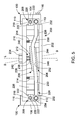
- FIG. 5 is a cross-sectional view of circuit card assembly 200 in an assembled configuration and mounted on chassis 100 by insertion into slot 112 defined between adjacent rails 110 of chassis 100.
- component layup 204 Prior to assembling circuit card assembly 200, component layup 204 is mounted on printed circuit board 202.
- Component layup 204 includes a suitable electronic component such as, for example, a processor 244 (or chip) soldered to printed circuit board 202 with at least one base component 246 such as, for example, a protective film or coating sandwiched between processor 244 and printed circuit board 202. Because processor 244 (and the various base components 246) are soldered or otherwise bonded to printed circuit board 202, it is possible that a plurality of layers of bonding material may exist between processor 244 and printed circuit board 202.
- a suitable electronic component such as, for example, a processor 244 (or chip) soldered to printed circuit board 202 with at least one base component 246 such as, for example, a protective film or coating sandwiched between processor 244 and
- processor 244 may not have a consistent thickness throughout, the height of processor 244 relative to printed circuit board 202 may be different at one region of processor 244 than at another region of processor 244, i.e., processor 244 may not be level or, in other words, may be tilted atop of printed circuit board 202 as shown in FIG. 5 .
- brace 212 is configured to automatically account for the tilted disposition of processor 244.
- circuit card assembly 200 is fabricated as follows. Brace 212 is coupled to frame 210 by inserting body 238 of bolt 236 into through-hole 216 of frame 210 for threadably coupling nut 234 to body 238 such that coil spring 242 is compressed between frame 210 and head 240. In this manner, the distance from head 240 to frame 210 and, therefore, the compression of coil spring 242 between head 240 and frame 210 is adjustable by rotating nut 234 relative to body 238.
- rotating nut 234 clockwise displaces (or retracts) head 240 toward frame 210 and compresses coil spring 242, and rotating nut 234 counterclockwise displaces (or protracts) head 240 away from frame 210 and decompresses coil spring 242.
- heat transfer device 206 is then coupled to frame 210 by inserting fasteners 214 through apertures 248 of support members 226 for fastening to frame 210 with wedge lock mechanisms 208 positioned between shoulders 218 of frame 210 and condensers 232 of heat pipes 224 so as to retain wedge lock mechanisms 208 between shoulders 218 and condensers 232.
- heat pipes 224 and contact member 228 are suspended between shoulders 218 by virtue of support members 226.
- nut 234 has already been sufficiently adjusted to maintain head 240 in spaced-apart relation with contact member 228 when heat transfer device 206 is coupled to frame 210, i.e., such that head 240 is not in contact with contact member 228 upon the coupling of heat transfer device 206 to frame 210.
- printed circuit board 202 (with component layup 204 mounted thereon) is then coupled to frame 210 by inserting fasteners 214 through apertures 250 in printed circuit board 202 for fastening to frame 210.
- processor 244 may or may not contact heat pipes 224 adjacent contact member 228. More specifically, once printed circuit board 202 has been coupled to frame 210, a gap may exist between processor 244 and heat pipes 224 in some embodiments, or processor 244 may be seated against heat pipes 224 in other embodiments.
- processor 244 is seated against heat pipes 224, the tilted (or not level) disposition of processor 244 relative to printed circuit board 202 renders the contact between processor 244 and heat pipes 224 to be non-uniform, i.e., some regions of a top surface 252 of processor 244 may be in contact with heat pipes 224 while other regions of top surface 252 may not be in contact with heat pipes 224 due to processor 244 being tilted relative to printed circuit board 202.
- nut 234 may be rotated to permit decompression of coil spring 242, thereby increasing the distance between head 240 and frame 210 until head 240 comes into contact with contact member 228 of heat transfer device 206. If a gap or non-uniform contact exists between processor 244 and heat pipes 224, head 240 displaces contact member 228 toward processor 244 and, therefore, bends the suspended segments of heat pipes 224 toward processor 244, so as to partially displace heat pipes 224 into an orientation that better conforms with the tilted orientation of processor 244.
- head 240 and contact member 228 convert what was a biasing force of brace 212 along longitudinal axis L into a biasing force along a bias axis B that is substantially normal to top surface 252 of processor 244, with longitudinal axis L and bias axis B being oblique relative to one another.
- brace 212 is said to be pivotable, automatically adjusting the direction of the applied biasing force in conformance with the tilt angle of processor 244 in order to facilitate imparting the biasing force normal to top surface 252 of processor 244 even when processor 244 is tilted relative to printed circuit board 202.
- brace 212 enables heat pipes 224 to be bent into an orientation that increases the physical contact between processor 244 and heat pipes 224 to facilitate improved heat transfer between processor 244 and heat pipes 224 during operation of processor 244.
- heat pipes 224 are in direct contact with processor 244 (without the presence of a buffer therebetween) to facilitate maximizing heat transfer. In other embodiments, however, heat pipes 224 may not be in direct contact with processor 244 but, rather, may have a spreader plate or other suitable buffer disposed between heat pipes 224 and processor 244.
- circuit card assembly 200 is said to be completely fabricated.
- Circuit card assembly 200 may then be inserted into slot 112 of chassis 100 between rails 110 of housing 102.
- wedge lock mechanisms 208 are to be activated by rotating core 220 of each wedge lock mechanism 208, e.g., using a hex key, to drive follower members 222 of the associated wedge lock mechanism 208 away from core 220 (and one another), thereby expanding wedge lock mechanisms 208 and locking circuit card assembly 200 into slot 112.
- circuit card assembly 200 is removable from chassis 100 for upgrade, repair, or replacement by rotating core 220 in the opposite direction to retract follower members 222 toward core 220 (and one another).
- processor 244 During operation of an electronics system such as, for example and without limitation, an avionics system of an aircraft utilizing circuit card assembly 200, processor 244 generates heat, and the heat is transferred away from processor 244 using heat pipes 224. More specifically, processor 244 heats heat pipes 224 at the location where heat pipes 224 are in physical contact with processor 244, thereby creating an evaporator region of each heat pipe 224 adjacent contact member 228. The working liquid permeating membrane 254 within heat pipes 224 in the evaporator regions vaporizes, and the vapor travels toward condenser(s) 232 in a lengthwise direction along bodies 230 of heat pipes 224.
- each condenser 232 Because each condenser 232 is in contact with one wall 104, 106 and one associated rail 110 of chassis 100, each condenser 232 has a temperature that is cooler than the temperature of the vapor within body 230, thereby condensing the vapor.
- the condensate that results, i.e., the working liquid is then wicked from condensers 232 toward the evaporator regions, i.e., toward processor 244, by virtue of the capillaries in membrane 254 such that the working liquid is again heated near processor 244.
- each heat pipe 224 maintains a cycle of vaporizing, condensing, and wicking the working liquid to transfer heat along the length of body 230.
- printed circuit board 202 may have one or more component layup 204 on either side, such that circuit card assembly 200 has one or more heat transfer device 206, one or more frame 210, and/or one or more brace 212 associated with each side of printed circuit board 202.
- any suitable combination of one or more heat transfer devices 206, one or more frames 210, and/or one or more braces 212 may be used to cool processors 244.
- the above-described embodiments facilitate providing a brace and a heat transfer device that account for manufacturing tolerances and other variables associated with fabricating a circuit card assembly.
- the devices, systems, and methods disclosed herein further facilitate reducing inconsistencies (such as gaps) in the contact between an electronic component of a circuit card assembly and the heat transfer device dedicated to cooling the electronic component.
- the devices, systems, and methods also facilitate providing a system configured to automatically adjust the contact between an electronic component disposed on a printed circuit board and a heat transfer device dedicated to cooling the electronic component.
- the embodiments disclosed herein further facilitate providing a cooling system having a self-adjustable brace configured to supply a biasing force that slightly deforms an annealed copper heat pipe to enable the heat pipe to make better contact with the electronic component for which the heat pipe is to provide cooling. Additionally, the embodiments facilitate reducing thermal resistance in a processor of a circuit card assembly so as to mitigate the temperature increase of the processor during operation, thereby increasing processor power. The above-described embodiments also facilitate enabling an avionics system to function more effectively in military environments having extreme temperature gradients and high shock/vibration, thereby improving the reliability of the avionics system.
- circuit card assemblies and methods of fabricating the same are described above in detail.
- the systems and methods are not limited to the specific embodiments described herein, but rather, components of the systems and/or steps of the methods may be utilized independently and separately from other components and/or steps described herein.
- the methods may also be used in combination with other systems, and are not limited to practice with only the aircraft-related systems described herein. Rather, the embodiments may be implemented and utilized in connection with many other applications outside of aviation.
Landscapes
- Engineering & Computer Science (AREA)
- Microelectronics & Electronic Packaging (AREA)
- Aviation & Aerospace Engineering (AREA)
- Physics & Mathematics (AREA)
- Thermal Sciences (AREA)
- Cooling Or The Like Of Electrical Apparatus (AREA)
Applications Claiming Priority (1)
| Application Number | Priority Date | Filing Date | Title |
|---|---|---|---|
| US14/068,697 US9253871B2 (en) | 2013-10-31 | 2013-10-31 | Circuit card assembly and method of fabricating the same |
Publications (2)
| Publication Number | Publication Date |
|---|---|
| EP2869680A1 true EP2869680A1 (de) | 2015-05-06 |
| EP2869680B1 EP2869680B1 (de) | 2019-07-31 |
Family
ID=51844552
Family Applications (1)
| Application Number | Title | Priority Date | Filing Date |
|---|---|---|---|
| EP14190939.0A Active EP2869680B1 (de) | 2013-10-31 | 2014-10-29 | Schaltkartenanordnung und Verfahren zur Herstellung davon |
Country Status (2)
| Country | Link |
|---|---|
| US (1) | US9253871B2 (de) |
| EP (1) | EP2869680B1 (de) |
Families Citing this family (14)
| Publication number | Priority date | Publication date | Assignee | Title |
|---|---|---|---|---|
| US9826662B2 (en) * | 2013-12-12 | 2017-11-21 | General Electric Company | Reusable phase-change thermal interface structures |
| US10327357B2 (en) * | 2014-09-18 | 2019-06-18 | Artesyn Embedded Computing, Inc. | Thermal conduction to a cylindrical shaft |
| DE102015202142A1 (de) * | 2015-02-06 | 2016-08-11 | Mahle International Gmbh | Elektrische Einrichtung |
| US9835382B2 (en) * | 2015-09-16 | 2017-12-05 | Acer Incorporated | Thermal dissipation module |
| US9750127B2 (en) | 2015-12-04 | 2017-08-29 | General Electric Company | Circuit card assembly including heat transfer assembly and method of manufacturing such |
| WO2018018163A2 (en) * | 2016-07-29 | 2018-02-01 | Adc Technologies Inc. | Fanless rail cooled electronics apparatus |
| US11063495B2 (en) * | 2019-07-01 | 2021-07-13 | Nidec Motor Corporation | Heatsink clamp for multiple electronic components |
| CN113347848B (zh) * | 2020-02-18 | 2024-10-25 | 四零四科技股份有限公司 | 具有可活动导热组件的电子装置及其相关的散热模块 |
| TWI718873B (zh) * | 2020-02-18 | 2021-02-11 | 四零四科技股份有限公司 | 具有可活動導熱組件的電子裝置及其相關的散熱模組 |
| CN111447777A (zh) * | 2020-04-03 | 2020-07-24 | 万安裕维电子有限公司 | 一种自清洁pcb板 |
| US12457709B2 (en) * | 2022-03-25 | 2025-10-28 | Nio Technology (Anhui) Co., Ltd. | Thermal transfer device for electronic processors |
| US11997812B2 (en) | 2022-10-12 | 2024-05-28 | Lunar Energy, Inc. | Cover for sealing a power module |
| US11889662B1 (en) | 2022-10-12 | 2024-01-30 | Lunar Energy, Inc. | Thermal interface sandwich |
| US11849536B1 (en) * | 2022-10-12 | 2023-12-19 | Lunar Energy, Inc. | Gantry for thermal management |
Citations (3)
| Publication number | Priority date | Publication date | Assignee | Title |
|---|---|---|---|---|
| US20040120116A1 (en) * | 2002-12-19 | 2004-06-24 | Chad St. Louis | Embedded heat pipe for a conduction cooled circuit card assembly |
| US20110182033A1 (en) * | 2007-12-18 | 2011-07-28 | Thales | Device for cooling an electronic card by conduction comprising heat pipes, and corresponding method of fabrication |
| US20120125586A1 (en) * | 2010-11-19 | 2012-05-24 | Inventec Corporation | Separable liquid-cooling heat-dissipation module |
Family Cites Families (14)
| Publication number | Priority date | Publication date | Assignee | Title |
|---|---|---|---|---|
| US5181167A (en) | 1991-12-02 | 1993-01-19 | Sun Microsystems, Inc. | Stacking heatpipe for three dimensional electronic packaging |
| US5764482A (en) | 1996-07-24 | 1998-06-09 | Thermacore, Inc. | Integrated circuit heat seat |
| JP2001085877A (ja) | 1999-09-10 | 2001-03-30 | Furukawa Electric Co Ltd:The | 突起部を有する受熱面を備えたヒートシンク |
| US6226178B1 (en) | 1999-10-12 | 2001-05-01 | Dell Usa, L.P. | Apparatus for cooling a heat generating component in a computer |
| US7232332B2 (en) * | 2003-01-07 | 2007-06-19 | Sun Microsystems, Inc. | Support and grounding structure |
| DE10327530A1 (de) | 2003-06-17 | 2005-01-20 | Electrovac Gesmbh | Vorrichtung mit wenigstens einer von einem zu kühlenden Funktionselement gebildeten Wärmequelle, mit wenigstens einer Wärmesenke und mit wenigstens einer Zwischenlage aus einer thermischen leitenden Masse zwischen der Wärmequelle und der Wärmesenke sowie thermische leitende Masse, insbesondere zur Verwendung bei einer solchen Vorrichtung |
| EP1859336A2 (de) | 2005-03-07 | 2007-11-28 | Asetek A/S | Kühlsystem für elektronische geräte, insbesondere computer |
| CN101584097B (zh) | 2006-11-10 | 2013-08-14 | 德雷格医疗系统股份有限公司 | 便携式设备冷却系统 |
| US7679916B2 (en) | 2006-12-08 | 2010-03-16 | GE Intelligent Platforms Embedded Systems, Inc. | Method and system for extracting heat from electrical components |
| US8223494B2 (en) | 2007-12-31 | 2012-07-17 | General Electric Company | Conduction cooled circuit board assembly |
| US7613001B1 (en) * | 2008-05-12 | 2009-11-03 | Fu Zhun Precision Industry (Shen Zhen) Co., Ltd. | Heat dissipation device with heat pipe |
| JP4812138B2 (ja) | 2008-09-24 | 2011-11-09 | 株式会社日立製作所 | 冷却装置及びそれを備えた電子機器 |
| US20110162828A1 (en) | 2010-01-06 | 2011-07-07 | Graham Charles Kirk | Thermal plug for use with a heat sink and method of assembling same |
| US20120155029A1 (en) | 2010-12-20 | 2012-06-21 | Raytheon Company | Adaptive thermal gap pad |
-
2013
- 2013-10-31 US US14/068,697 patent/US9253871B2/en active Active
-
2014
- 2014-10-29 EP EP14190939.0A patent/EP2869680B1/de active Active
Patent Citations (3)
| Publication number | Priority date | Publication date | Assignee | Title |
|---|---|---|---|---|
| US20040120116A1 (en) * | 2002-12-19 | 2004-06-24 | Chad St. Louis | Embedded heat pipe for a conduction cooled circuit card assembly |
| US20110182033A1 (en) * | 2007-12-18 | 2011-07-28 | Thales | Device for cooling an electronic card by conduction comprising heat pipes, and corresponding method of fabrication |
| US20120125586A1 (en) * | 2010-11-19 | 2012-05-24 | Inventec Corporation | Separable liquid-cooling heat-dissipation module |
Also Published As
| Publication number | Publication date |
|---|---|
| US9253871B2 (en) | 2016-02-02 |
| EP2869680B1 (de) | 2019-07-31 |
| US20150116940A1 (en) | 2015-04-30 |
Similar Documents
| Publication | Publication Date | Title |
|---|---|---|
| EP2869680B1 (de) | Schaltkartenanordnung und Verfahren zur Herstellung davon | |
| JP4881879B2 (ja) | 冷却装置、システムおよび関連する方法 | |
| JP5372472B2 (ja) | 伝導冷却回路基板構体 | |
| JP5329738B2 (ja) | 熱移送装置 | |
| US7019973B2 (en) | Circuit cooling apparatus | |
| US8919426B2 (en) | Micro-channel pulsating heat pipe | |
| US9333599B2 (en) | Electronics chassis and method of fabricating the same | |
| Ju et al. | Planar vapor chamber with hybrid evaporator wicks for the thermal management of high-heat-flux and high-power optoelectronic devices | |
| US8223494B2 (en) | Conduction cooled circuit board assembly | |
| EP3869550B1 (de) | Lastausgleichsvorrichtung für wärmesenke | |
| US8739405B2 (en) | Method of manufacturing an evaporator for looped heat pipe | |
| WO2006072244A1 (en) | A multi-orientational cooling system with a bubble pump | |
| JP2005326141A (ja) | 配管とベローズを用いた液体冷却ループ装置 | |
| US9772143B2 (en) | Thermal module | |
| Shi et al. | An experimental investigation of thermal performance of a polymer‐based flat heat pipe | |
| CN110160576A (zh) | 用于将传感器组件安装在运输工具上的传感器系统 | |
| US20160146545A1 (en) | Mechanical fastener | |
| US20150034278A1 (en) | Heat pipe matrix for electronics cooling | |
| JP7191511B2 (ja) | 二相流体受動冷却システム、特に、航空電子機器等の電子機器を冷却するための二相流体受動冷却システム | |
| WO2016143070A1 (ja) | 電力変換装置及び冷凍サイクル装置 | |
| Ku | Introduction to heat pipes | |
| US20030062150A1 (en) | Temperature/strain control of fatigue vulnerable devices used in electronic circuits | |
| JP2007263427A (ja) | ループ型ヒートパイプ | |
| JP2005114179A (ja) | ヒートパイプ | |
| US20090269050A1 (en) | Camera Unit |
Legal Events
| Date | Code | Title | Description |
|---|---|---|---|
| PUAI | Public reference made under article 153(3) epc to a published international application that has entered the european phase |
Free format text: ORIGINAL CODE: 0009012 |
|
| 17P | Request for examination filed |
Effective date: 20141029 |
|
| AK | Designated contracting states |
Kind code of ref document: A1 Designated state(s): AL AT BE BG CH CY CZ DE DK EE ES FI FR GB GR HR HU IE IS IT LI LT LU LV MC MK MT NL NO PL PT RO RS SE SI SK SM TR |
|
| AX | Request for extension of the european patent |
Extension state: BA ME |
|
| R17P | Request for examination filed (corrected) |
Effective date: 20151106 |
|
| RBV | Designated contracting states (corrected) |
Designated state(s): AL AT BE BG CH CY CZ DE DK EE ES FI FR GB GR HR HU IE IS IT LI LT LU LV MC MK MT NL NO PL PT RO RS SE SI SK SM TR |
|
| REG | Reference to a national code |
Ref country code: DE Ref legal event code: R079 Ref document number: 602014050777 Country of ref document: DE Free format text: PREVIOUS MAIN CLASS: H05K0007140000 Ipc: H05K0001020000 |
|
| GRAP | Despatch of communication of intention to grant a patent |
Free format text: ORIGINAL CODE: EPIDOSNIGR1 |
|
| STAA | Information on the status of an ep patent application or granted ep patent |
Free format text: STATUS: GRANT OF PATENT IS INTENDED |
|
| RIC1 | Information provided on ipc code assigned before grant |
Ipc: H05K 7/20 20060101ALI20190117BHEP Ipc: H05K 7/14 20060101ALI20190117BHEP Ipc: H05K 1/02 20060101AFI20190117BHEP |
|
| INTG | Intention to grant announced |
Effective date: 20190215 |
|
| GRAS | Grant fee paid |
Free format text: ORIGINAL CODE: EPIDOSNIGR3 |
|
| GRAA | (expected) grant |
Free format text: ORIGINAL CODE: 0009210 |
|
| STAA | Information on the status of an ep patent application or granted ep patent |
Free format text: STATUS: THE PATENT HAS BEEN GRANTED |
|
| AK | Designated contracting states |
Kind code of ref document: B1 Designated state(s): AL AT BE BG CH CY CZ DE DK EE ES FI FR GB GR HR HU IE IS IT LI LT LU LV MC MK MT NL NO PL PT RO RS SE SI SK SM TR |
|
| REG | Reference to a national code |
Ref country code: CH Ref legal event code: EP Ref country code: GB Ref legal event code: FG4D |
|
| REG | Reference to a national code |
Ref country code: AT Ref legal event code: REF Ref document number: 1162401 Country of ref document: AT Kind code of ref document: T Effective date: 20190815 |
|
| REG | Reference to a national code |
Ref country code: IE Ref legal event code: FG4D |
|
| REG | Reference to a national code |
Ref country code: DE Ref legal event code: R096 Ref document number: 602014050777 Country of ref document: DE |
|
| REG | Reference to a national code |
Ref country code: NL Ref legal event code: MP Effective date: 20190731 |
|
| REG | Reference to a national code |
Ref country code: LT Ref legal event code: MG4D |
|
| REG | Reference to a national code |
Ref country code: AT Ref legal event code: MK05 Ref document number: 1162401 Country of ref document: AT Kind code of ref document: T Effective date: 20190731 |
|
| PG25 | Lapsed in a contracting state [announced via postgrant information from national office to epo] |
Ref country code: LT Free format text: LAPSE BECAUSE OF FAILURE TO SUBMIT A TRANSLATION OF THE DESCRIPTION OR TO PAY THE FEE WITHIN THE PRESCRIBED TIME-LIMIT Effective date: 20190731 Ref country code: HR Free format text: LAPSE BECAUSE OF FAILURE TO SUBMIT A TRANSLATION OF THE DESCRIPTION OR TO PAY THE FEE WITHIN THE PRESCRIBED TIME-LIMIT Effective date: 20190731 Ref country code: AT Free format text: LAPSE BECAUSE OF FAILURE TO SUBMIT A TRANSLATION OF THE DESCRIPTION OR TO PAY THE FEE WITHIN THE PRESCRIBED TIME-LIMIT Effective date: 20190731 Ref country code: NO Free format text: LAPSE BECAUSE OF FAILURE TO SUBMIT A TRANSLATION OF THE DESCRIPTION OR TO PAY THE FEE WITHIN THE PRESCRIBED TIME-LIMIT Effective date: 20191031 Ref country code: NL Free format text: LAPSE BECAUSE OF FAILURE TO SUBMIT A TRANSLATION OF THE DESCRIPTION OR TO PAY THE FEE WITHIN THE PRESCRIBED TIME-LIMIT Effective date: 20190731 Ref country code: BG Free format text: LAPSE BECAUSE OF FAILURE TO SUBMIT A TRANSLATION OF THE DESCRIPTION OR TO PAY THE FEE WITHIN THE PRESCRIBED TIME-LIMIT Effective date: 20191031 Ref country code: PT Free format text: LAPSE BECAUSE OF FAILURE TO SUBMIT A TRANSLATION OF THE DESCRIPTION OR TO PAY THE FEE WITHIN THE PRESCRIBED TIME-LIMIT Effective date: 20191202 Ref country code: FI Free format text: LAPSE BECAUSE OF FAILURE TO SUBMIT A TRANSLATION OF THE DESCRIPTION OR TO PAY THE FEE WITHIN THE PRESCRIBED TIME-LIMIT Effective date: 20190731 Ref country code: SE Free format text: LAPSE BECAUSE OF FAILURE TO SUBMIT A TRANSLATION OF THE DESCRIPTION OR TO PAY THE FEE WITHIN THE PRESCRIBED TIME-LIMIT Effective date: 20190731 |
|
| PG25 | Lapsed in a contracting state [announced via postgrant information from national office to epo] |
Ref country code: RS Free format text: LAPSE BECAUSE OF FAILURE TO SUBMIT A TRANSLATION OF THE DESCRIPTION OR TO PAY THE FEE WITHIN THE PRESCRIBED TIME-LIMIT Effective date: 20190731 Ref country code: AL Free format text: LAPSE BECAUSE OF FAILURE TO SUBMIT A TRANSLATION OF THE DESCRIPTION OR TO PAY THE FEE WITHIN THE PRESCRIBED TIME-LIMIT Effective date: 20190731 Ref country code: IS Free format text: LAPSE BECAUSE OF FAILURE TO SUBMIT A TRANSLATION OF THE DESCRIPTION OR TO PAY THE FEE WITHIN THE PRESCRIBED TIME-LIMIT Effective date: 20191130 Ref country code: ES Free format text: LAPSE BECAUSE OF FAILURE TO SUBMIT A TRANSLATION OF THE DESCRIPTION OR TO PAY THE FEE WITHIN THE PRESCRIBED TIME-LIMIT Effective date: 20190731 Ref country code: LV Free format text: LAPSE BECAUSE OF FAILURE TO SUBMIT A TRANSLATION OF THE DESCRIPTION OR TO PAY THE FEE WITHIN THE PRESCRIBED TIME-LIMIT Effective date: 20190731 Ref country code: GR Free format text: LAPSE BECAUSE OF FAILURE TO SUBMIT A TRANSLATION OF THE DESCRIPTION OR TO PAY THE FEE WITHIN THE PRESCRIBED TIME-LIMIT Effective date: 20191101 |
|
| PG25 | Lapsed in a contracting state [announced via postgrant information from national office to epo] |
Ref country code: TR Free format text: LAPSE BECAUSE OF FAILURE TO SUBMIT A TRANSLATION OF THE DESCRIPTION OR TO PAY THE FEE WITHIN THE PRESCRIBED TIME-LIMIT Effective date: 20190731 |
|
| PG25 | Lapsed in a contracting state [announced via postgrant information from national office to epo] |
Ref country code: EE Free format text: LAPSE BECAUSE OF FAILURE TO SUBMIT A TRANSLATION OF THE DESCRIPTION OR TO PAY THE FEE WITHIN THE PRESCRIBED TIME-LIMIT Effective date: 20190731 Ref country code: DK Free format text: LAPSE BECAUSE OF FAILURE TO SUBMIT A TRANSLATION OF THE DESCRIPTION OR TO PAY THE FEE WITHIN THE PRESCRIBED TIME-LIMIT Effective date: 20190731 Ref country code: IT Free format text: LAPSE BECAUSE OF FAILURE TO SUBMIT A TRANSLATION OF THE DESCRIPTION OR TO PAY THE FEE WITHIN THE PRESCRIBED TIME-LIMIT Effective date: 20190731 Ref country code: RO Free format text: LAPSE BECAUSE OF FAILURE TO SUBMIT A TRANSLATION OF THE DESCRIPTION OR TO PAY THE FEE WITHIN THE PRESCRIBED TIME-LIMIT Effective date: 20190731 Ref country code: PL Free format text: LAPSE BECAUSE OF FAILURE TO SUBMIT A TRANSLATION OF THE DESCRIPTION OR TO PAY THE FEE WITHIN THE PRESCRIBED TIME-LIMIT Effective date: 20190731 |
|
| PG25 | Lapsed in a contracting state [announced via postgrant information from national office to epo] |
Ref country code: SK Free format text: LAPSE BECAUSE OF FAILURE TO SUBMIT A TRANSLATION OF THE DESCRIPTION OR TO PAY THE FEE WITHIN THE PRESCRIBED TIME-LIMIT Effective date: 20190731 Ref country code: MC Free format text: LAPSE BECAUSE OF FAILURE TO SUBMIT A TRANSLATION OF THE DESCRIPTION OR TO PAY THE FEE WITHIN THE PRESCRIBED TIME-LIMIT Effective date: 20190731 Ref country code: IS Free format text: LAPSE BECAUSE OF FAILURE TO SUBMIT A TRANSLATION OF THE DESCRIPTION OR TO PAY THE FEE WITHIN THE PRESCRIBED TIME-LIMIT Effective date: 20200224 Ref country code: CZ Free format text: LAPSE BECAUSE OF FAILURE TO SUBMIT A TRANSLATION OF THE DESCRIPTION OR TO PAY THE FEE WITHIN THE PRESCRIBED TIME-LIMIT Effective date: 20190731 Ref country code: SM Free format text: LAPSE BECAUSE OF FAILURE TO SUBMIT A TRANSLATION OF THE DESCRIPTION OR TO PAY THE FEE WITHIN THE PRESCRIBED TIME-LIMIT Effective date: 20190731 |
|
| REG | Reference to a national code |
Ref country code: CH Ref legal event code: PL |
|
| REG | Reference to a national code |
Ref country code: DE Ref legal event code: R097 Ref document number: 602014050777 Country of ref document: DE |
|
| PLBE | No opposition filed within time limit |
Free format text: ORIGINAL CODE: 0009261 |
|
| STAA | Information on the status of an ep patent application or granted ep patent |
Free format text: STATUS: NO OPPOSITION FILED WITHIN TIME LIMIT |
|
| PG2D | Information on lapse in contracting state deleted |
Ref country code: IS |
|
| PG25 | Lapsed in a contracting state [announced via postgrant information from national office to epo] |
Ref country code: CH Free format text: LAPSE BECAUSE OF NON-PAYMENT OF DUE FEES Effective date: 20191031 Ref country code: LU Free format text: LAPSE BECAUSE OF NON-PAYMENT OF DUE FEES Effective date: 20191029 Ref country code: LI Free format text: LAPSE BECAUSE OF NON-PAYMENT OF DUE FEES Effective date: 20191031 Ref country code: IS Free format text: LAPSE BECAUSE OF FAILURE TO SUBMIT A TRANSLATION OF THE DESCRIPTION OR TO PAY THE FEE WITHIN THE PRESCRIBED TIME-LIMIT Effective date: 20191030 |
|
| 26N | No opposition filed |
Effective date: 20200603 |
|
| REG | Reference to a national code |
Ref country code: BE Ref legal event code: MM Effective date: 20191031 |
|
| PG25 | Lapsed in a contracting state [announced via postgrant information from national office to epo] |
Ref country code: SI Free format text: LAPSE BECAUSE OF FAILURE TO SUBMIT A TRANSLATION OF THE DESCRIPTION OR TO PAY THE FEE WITHIN THE PRESCRIBED TIME-LIMIT Effective date: 20190731 Ref country code: BE Free format text: LAPSE BECAUSE OF NON-PAYMENT OF DUE FEES Effective date: 20191031 |
|
| PG25 | Lapsed in a contracting state [announced via postgrant information from national office to epo] |
Ref country code: IE Free format text: LAPSE BECAUSE OF NON-PAYMENT OF DUE FEES Effective date: 20191029 |
|
| PG25 | Lapsed in a contracting state [announced via postgrant information from national office to epo] |
Ref country code: CY Free format text: LAPSE BECAUSE OF FAILURE TO SUBMIT A TRANSLATION OF THE DESCRIPTION OR TO PAY THE FEE WITHIN THE PRESCRIBED TIME-LIMIT Effective date: 20190731 |
|
| PG25 | Lapsed in a contracting state [announced via postgrant information from national office to epo] |
Ref country code: MT Free format text: LAPSE BECAUSE OF FAILURE TO SUBMIT A TRANSLATION OF THE DESCRIPTION OR TO PAY THE FEE WITHIN THE PRESCRIBED TIME-LIMIT Effective date: 20190731 Ref country code: HU Free format text: LAPSE BECAUSE OF FAILURE TO SUBMIT A TRANSLATION OF THE DESCRIPTION OR TO PAY THE FEE WITHIN THE PRESCRIBED TIME-LIMIT; INVALID AB INITIO Effective date: 20141029 |
|
| PG25 | Lapsed in a contracting state [announced via postgrant information from national office to epo] |
Ref country code: MK Free format text: LAPSE BECAUSE OF FAILURE TO SUBMIT A TRANSLATION OF THE DESCRIPTION OR TO PAY THE FEE WITHIN THE PRESCRIBED TIME-LIMIT Effective date: 20190731 |
|
| P01 | Opt-out of the competence of the unified patent court (upc) registered |
Effective date: 20230414 |
|
| PGFP | Annual fee paid to national office [announced via postgrant information from national office to epo] |
Ref country code: GB Payment date: 20250923 Year of fee payment: 12 |
|
| PGFP | Annual fee paid to national office [announced via postgrant information from national office to epo] |
Ref country code: FR Payment date: 20250924 Year of fee payment: 12 |
|
| PGFP | Annual fee paid to national office [announced via postgrant information from national office to epo] |
Ref country code: DE Payment date: 20250923 Year of fee payment: 12 |