EP2862014B1 - Procédés et appareil assurant l'isolation thermique de dispositifs photoniques - Google Patents
Procédés et appareil assurant l'isolation thermique de dispositifs photoniques Download PDFInfo
- Publication number
- EP2862014B1 EP2862014B1 EP13733154.2A EP13733154A EP2862014B1 EP 2862014 B1 EP2862014 B1 EP 2862014B1 EP 13733154 A EP13733154 A EP 13733154A EP 2862014 B1 EP2862014 B1 EP 2862014B1
- Authority
- EP
- European Patent Office
- Prior art keywords
- substrate
- isolation region
- thermal isolation
- heating device
- region
- Prior art date
- Legal status (The legal status is an assumption and is not a legal conclusion. Google has not performed a legal analysis and makes no representation as to the accuracy of the status listed.)
- Active
Links
Images


Classifications
-
- G—PHYSICS
- G02—OPTICS
- G02B—OPTICAL ELEMENTS, SYSTEMS OR APPARATUS
- G02B6/00—Light guides; Structural details of arrangements comprising light guides and other optical elements, e.g. couplings
- G02B6/10—Light guides; Structural details of arrangements comprising light guides and other optical elements, e.g. couplings of the optical waveguide type
- G02B6/12—Light guides; Structural details of arrangements comprising light guides and other optical elements, e.g. couplings of the optical waveguide type of the integrated circuit kind
- G02B6/12007—Light guides; Structural details of arrangements comprising light guides and other optical elements, e.g. couplings of the optical waveguide type of the integrated circuit kind forming wavelength selective elements, e.g. multiplexer, demultiplexer
-
- H—ELECTRICITY
- H01—ELECTRIC ELEMENTS
- H01L—SEMICONDUCTOR DEVICES NOT COVERED BY CLASS H10
- H01L33/00—Semiconductor devices with at least one potential-jump barrier or surface barrier specially adapted for light emission; Processes or apparatus specially adapted for the manufacture or treatment thereof or of parts thereof; Details thereof
- H01L33/48—Semiconductor devices with at least one potential-jump barrier or surface barrier specially adapted for light emission; Processes or apparatus specially adapted for the manufacture or treatment thereof or of parts thereof; Details thereof characterised by the semiconductor body packages
- H01L33/64—Heat extraction or cooling elements
-
- G—PHYSICS
- G02—OPTICS
- G02B—OPTICAL ELEMENTS, SYSTEMS OR APPARATUS
- G02B6/00—Light guides; Structural details of arrangements comprising light guides and other optical elements, e.g. couplings
- G02B6/10—Light guides; Structural details of arrangements comprising light guides and other optical elements, e.g. couplings of the optical waveguide type
- G02B6/12—Light guides; Structural details of arrangements comprising light guides and other optical elements, e.g. couplings of the optical waveguide type of the integrated circuit kind
- G02B6/12004—Combinations of two or more optical elements
-
- G—PHYSICS
- G02—OPTICS
- G02F—OPTICAL DEVICES OR ARRANGEMENTS FOR THE CONTROL OF LIGHT BY MODIFICATION OF THE OPTICAL PROPERTIES OF THE MEDIA OF THE ELEMENTS INVOLVED THEREIN; NON-LINEAR OPTICS; FREQUENCY-CHANGING OF LIGHT; OPTICAL LOGIC ELEMENTS; OPTICAL ANALOGUE/DIGITAL CONVERTERS
- G02F1/00—Devices or arrangements for the control of the intensity, colour, phase, polarisation or direction of light arriving from an independent light source, e.g. switching, gating or modulating; Non-linear optics
- G02F1/01—Devices or arrangements for the control of the intensity, colour, phase, polarisation or direction of light arriving from an independent light source, e.g. switching, gating or modulating; Non-linear optics for the control of the intensity, phase, polarisation or colour
- G02F1/0147—Devices or arrangements for the control of the intensity, colour, phase, polarisation or direction of light arriving from an independent light source, e.g. switching, gating or modulating; Non-linear optics for the control of the intensity, phase, polarisation or colour based on thermo-optic effects
-
- G—PHYSICS
- G02—OPTICS
- G02F—OPTICAL DEVICES OR ARRANGEMENTS FOR THE CONTROL OF LIGHT BY MODIFICATION OF THE OPTICAL PROPERTIES OF THE MEDIA OF THE ELEMENTS INVOLVED THEREIN; NON-LINEAR OPTICS; FREQUENCY-CHANGING OF LIGHT; OPTICAL LOGIC ELEMENTS; OPTICAL ANALOGUE/DIGITAL CONVERTERS
- G02F1/00—Devices or arrangements for the control of the intensity, colour, phase, polarisation or direction of light arriving from an independent light source, e.g. switching, gating or modulating; Non-linear optics
- G02F1/29—Devices or arrangements for the control of the intensity, colour, phase, polarisation or direction of light arriving from an independent light source, e.g. switching, gating or modulating; Non-linear optics for the control of the position or the direction of light beams, i.e. deflection
- G02F1/31—Digital deflection, i.e. optical switching
- G02F1/313—Digital deflection, i.e. optical switching in an optical waveguide structure
- G02F1/3132—Digital deflection, i.e. optical switching in an optical waveguide structure of directional coupler type
- G02F1/3133—Digital deflection, i.e. optical switching in an optical waveguide structure of directional coupler type the optical waveguides being made of semiconducting materials
-
- G—PHYSICS
- G02—OPTICS
- G02B—OPTICAL ELEMENTS, SYSTEMS OR APPARATUS
- G02B6/00—Light guides; Structural details of arrangements comprising light guides and other optical elements, e.g. couplings
- G02B6/10—Light guides; Structural details of arrangements comprising light guides and other optical elements, e.g. couplings of the optical waveguide type
- G02B6/12—Light guides; Structural details of arrangements comprising light guides and other optical elements, e.g. couplings of the optical waveguide type of the integrated circuit kind
- G02B2006/12035—Materials
- G02B2006/12038—Glass (SiO2 based materials)
-
- G—PHYSICS
- G02—OPTICS
- G02B—OPTICAL ELEMENTS, SYSTEMS OR APPARATUS
- G02B6/00—Light guides; Structural details of arrangements comprising light guides and other optical elements, e.g. couplings
- G02B6/10—Light guides; Structural details of arrangements comprising light guides and other optical elements, e.g. couplings of the optical waveguide type
- G02B6/12—Light guides; Structural details of arrangements comprising light guides and other optical elements, e.g. couplings of the optical waveguide type of the integrated circuit kind
- G02B2006/12083—Constructional arrangements
- G02B2006/121—Channel; buried or the like
-
- G—PHYSICS
- G02—OPTICS
- G02B—OPTICAL ELEMENTS, SYSTEMS OR APPARATUS
- G02B6/00—Light guides; Structural details of arrangements comprising light guides and other optical elements, e.g. couplings
- G02B6/10—Light guides; Structural details of arrangements comprising light guides and other optical elements, e.g. couplings of the optical waveguide type
- G02B6/12—Light guides; Structural details of arrangements comprising light guides and other optical elements, e.g. couplings of the optical waveguide type of the integrated circuit kind
- G02B2006/12133—Functions
- G02B2006/12135—Temperature control
-
- G—PHYSICS
- G02—OPTICS
- G02B—OPTICAL ELEMENTS, SYSTEMS OR APPARATUS
- G02B6/00—Light guides; Structural details of arrangements comprising light guides and other optical elements, e.g. couplings
- G02B6/10—Light guides; Structural details of arrangements comprising light guides and other optical elements, e.g. couplings of the optical waveguide type
- G02B6/12—Light guides; Structural details of arrangements comprising light guides and other optical elements, e.g. couplings of the optical waveguide type of the integrated circuit kind
- G02B6/13—Integrated optical circuits characterised by the manufacturing method
- G02B6/136—Integrated optical circuits characterised by the manufacturing method by etching
-
- G—PHYSICS
- G02—OPTICS
- G02F—OPTICAL DEVICES OR ARRANGEMENTS FOR THE CONTROL OF LIGHT BY MODIFICATION OF THE OPTICAL PROPERTIES OF THE MEDIA OF THE ELEMENTS INVOLVED THEREIN; NON-LINEAR OPTICS; FREQUENCY-CHANGING OF LIGHT; OPTICAL LOGIC ELEMENTS; OPTICAL ANALOGUE/DIGITAL CONVERTERS
- G02F2203/00—Function characteristic
- G02F2203/15—Function characteristic involving resonance effects, e.g. resonantly enhanced interaction
-
- H—ELECTRICITY
- H01—ELECTRIC ELEMENTS
- H01L—SEMICONDUCTOR DEVICES NOT COVERED BY CLASS H10
- H01L2933/00—Details relating to devices covered by the group H01L33/00 but not provided for in its subgroups
- H01L2933/0008—Processes
- H01L2933/0033—Processes relating to semiconductor body packages
- H01L2933/0075—Processes relating to semiconductor body packages relating to heat extraction or cooling elements
Definitions
- Described embodiments relate generally to the field of electronic-photonic devices, and more particularly to the thermal isolation of electronic-photonic devices.
- Optical transmission may be used as a means for communication between separate integrated circuit die (also referred to as inter-die connections), and between components on the same die (also referred to as intra-die connections).
- Photonic devices are a class of devices that are capable of sourcing, controlling, and/or detecting optical transmission of signals.
- silicon photonics relates to the study and application of photonic systems that use silicon as an optical medium. Instead of, or in addition to, using silicon to facilitate the flow of electricity, silicon can be used to direct the flow of photons or light. Silicon is transparent to infrared light with wavelengths above about 1.1 micrometers. Silicon also has a high refractive index of about 3.5. The tight optical confinement provided by this high index allows for microscopic optical waveguides, which may have cross-sectional dimensions of only a few hundred nanometers, thus facilitating integration with current nano-scale semiconductor technologies that also employ silicon, such as complementary metal oxide semiconductor (CMOS) technologies. Silicon photonic devices can thus be made using existing semiconductor fabrication techniques. Further, because silicon is already used as a substrate for many electronic integrated circuits, it is possible to create hybrid devices employing both optical and electronic components integrated onto a single die.
- CMOS complementary metal oxide semiconductor
- photonic devices are increasingly being integrated with optical/electrical circuits to form a type of electronic-photonic device called an electronic-photonic integrated circuit.
- an electronic-photonic integrated circuit For example, in the semiconductor industry, photonic devices have various applications including communication within a die, between multiple die of a computer board, and between computer boards.
- each die on the circuit board can be interfaced with a photonic-electronic transmitter-receiver circuit, with two die operably connected via an optical waveguide.
- optical waveguides may be used to connect components within a die, such as between an integrated optical source and a photonic detector.
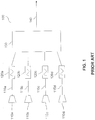
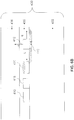
- FIG. 1 illustrates a block diagram of one example of a conventional photonic multiplexing system 100.
- the system 100 includes multiple carrier wave input devices 110a, 110b, 110c, 110d (generally referred to as an input device 110), each of which may be, for example, an optical source configured to generate an optical carrier wave at a respective transmission wavelength.
- each input device 110 may include a coherent light source, such as a laser (e.g., a hybrid silicon laser or a gallium arsenide laser), or other appropriate light source known in the art.
- a coherent light source such as a laser (e.g., a hybrid silicon laser or a gallium arsenide laser), or other appropriate light source known in the art.
- the optical carrier wave from each input device 110a-d is transmitted to a respective resonant carrier wave modulator 120a-d along a respective optical waveguide 115a-d.
- Carrier wave modulators 120a-d are configured to receive respective optical carrier waves having different wavelengths from the respective input devices 110a-d, and to modulate data on the optical carrier wave that it receives.
- carrier wave modulators 120a-d may be optical modulators configured to receive an optical data signal and output a modulated optical data signal, or electro-optical modulators configured to receive an electrical data signal from an electrically conductive interconnect and output a modulated optical data signal.
- the modulated light from each of the carrier wave modulators 120a-d is then combined and transmitted onto a single transmission channel (e.g., optical waveguide 140) using an optical multiplexer 130.
- the multiplexed light is transmitted along optical waveguide 140 to an endpoint (not shown) that may include, e.g., one or more photonic detectors for detecting optical transmissions, where the light is demultiplexed and demodulated before being used by an endpoint device.
- Wave guiding of an optical carrier wave through optical waveguides 115, 140 occurs through internal reflection of electromagnetic waves of an optical carrier wave at the interface between a higher refractive index inner core and a lower refractive index outer cladding.
- the inner core of an optical waveguide 115 may be formed of a silicon (Si) or silicon-containing material, and may have a refractive index of approximately 3.5.
- the cladding of an optical waveguide 115 may be formed of a material having a lower index of refraction, for example, a SiO 2 material with a refractive index of approximately 1.5.
- Several components within a photonic system can be affected by variations in temperature. Variations in temperature can result in changes in the device dimensions (due to thermal expansion) and refractive indices of materials.
- an optical laser providing one or more carrier wavelengths can be tuned by changing its temperature.
- changes in temperature can affect the operation of a resonant carrier wave modulator 120.
- the resonant frequency of a particular modulator 120 is controlled in part by the refractive indices of its resonant structures, which may change according to temperature, resulting in turn in a deviation of the resonant frequency of the modulator 120. Accordingly, certain photonic devices require a stable thermal environment to perform optimally.
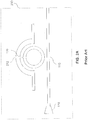
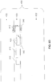
- FIG. 2A shows a top-down view of photonic devices including an input device 110 (e.g., a laser), an optical waveguide 115, and a resonant carrier wave modulator 120, formed in a portion of a silicon die 230.
- a heating device 212 provides active temperature control of carrier wave modulator 120.
- Heating device 212 may be, for example, a resistive or inductive element, such as a polysilicon, silicon, or copper element, that is configured to receive energy (e.g., electrical energy) and output heat to the surrounding photonic devices.
- energy e.g., electrical energy
- heating device 212 may be customized to modulator 120, by partially encircling modulator 120, or may have any other shape and be located near other temperature-sensitive photonic devices, as well as carrier wave modulator 120. In other embodiments, heating device 212 may be integrated with carrier wave modulator 120.
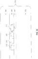
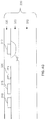
- FIG. 2B shows a cross-sectional view of photonic devices formed in a portion of a silicon on insulator (SOI) integrated circuit die 230.
- Die 230 includes an input device 110 (e.g., a laser), an optical waveguide 115, and a resonant carrier wave modulator 120.
- Die 230 includes a substrate 232, which may be, for example, a bulk region of thermally conductive silicon.
- the SOI structure also includes an insulator region 233 (also referred to as a buried oxide or "BOX" region) composed of an insulating material, such as SiO 2 , which acts as a bottom cladding layer for an optical waveguide 115.
- BOX buried oxide
- Die 230 may also include an interlevel dielectric (ILD) region 236 having a lower layer composed of, for example, SiO 2 , formed above the device formation layer 235.
- ILD region 236 provides an upper cladding region for optical waveguide 115, and upper levels of the ILD region 236 are used for forming electrical connections in various locations of die 230, such as above the device formation region 235.
- photonic devices including input device 110 (e.g., a laser), optical waveguide 115, and resonant carrier wave modulator 120, as well as heating device 212, are formed in the device formation region 235 above the substrate 232.
- Device formation region 235 may include regions of silicon for forming photonic devices, such as the inner core of optical waveguide 115 and modulator 120, and regions of a cladding material, such as SiO 2 , on the sides of optical waveguide 115 to serve as cladding surrounding a silicon waveguide core, and to serve as an insulating and mechanically supportive material for the devices formed in device formation region 235.
- Other photonic devices such as other optical waveguides, lasers, filters, or photonic detectors, may also be formed in the device formation region 235, and may be subjected to active temperature control using a heating device 212.
- heating device 212 provides active temperature control of one or more photonic devices, such as modulator 120, in device formation region 235, it emits heat q that dissipates in all directions, including into the substrate 232, which is formed of thermally conductive silicon, and into the ILD region 236. This results in wasted heat flux and a less efficient heating device 212. Additionally, photonic devices in die 230 are typically thermally coupled to the substrate 232, and any global temperature variation in the die 230 may have an effect on the photonic devices.
- Embodiments described herein include photonics devices and integrated circuits with a thermal isolation region for controlling dissipation of heat in a photonic system.
- a thermal isolation region may be formed near one or more temperature-sensitive photonic structures.
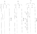
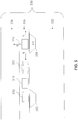
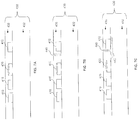
- FIGS. 3A and 3B illustrate one embodiment. They show a top-down view and a cross-sectional view, respectively, of photonic devices formed in a portion of a die 330.
- die 330 may include one or more temperature sensitive photonic devices of a photonic system, including, for example, a resonant carrier wave modulator 320, such as a ring resonator or disk resonator, or another type of resonant modulator.
- Carrier wave modulator 320 may be an electro-optical modulator configured to receive an electrical data signal from an electrically connected interconnect, such as an electrically conductive signal line, and modulate a carrier wave in an adjacent optical waveguide 315 according to the received data.
- carrier wave modulator 320 may be an optical modulator configured to receive an optical data signal, such as from another optical waveguide.
- Die 330 also includes one or more heating devices 312 providing active temperature control of one or more of the photonic devices, such as the carrier wave modulator 320.
- Heating device 312 can be a resistive element, such as a polysilicon, silicon, or copper element, that is configured to receive electrical energy from an electrically connected interconnect, such as a via, and output heat.
- carrier wave modulator 320 and heating device 312 are shown as separate elements FIG. 3A , it should be understood that heating device 312 may also be integrated with carrier wave modulator 320.
- Die 330 also includes a carrier wave input device 310, such as a laser configured to output an optical carrier wave, which is another example of a temperature sensitive photonic device. Die 330 also includes an optical waveguide 315 configured to carry an optical carrier wave that is modulated by the carrier wave modulator 320. It should be understood that the described temperature-sensitive photonic devices, structures, and arrangements are merely exemplary, and the embodiments below may be applied in connection with any known temperature-sensitive photonic structures, including, e.g., temperature-sensitive photonic detectors, optical waveguides, filters, or other structures.
- the photonic devices such as input device 310, optical waveguide 315, and waveguide modulator 320, as well as heating device 312, may be formed in an integrated circuit.
- Die 330 includes a substrate 332, which may be, for example, a bulk region of thermally conductive silicon.
- substrate 332 may optionally include an insulator or "BOX" region 233 ( FIG. 2B ) composed of an electrically insulating material, such as SiO 2 , providing a silicon-on-insulator (SOI) substrate.
- Photonic devices including input device 310, optical waveguide 315, and waveguide modulator 320 are formed in a device formation region 335 above a portion of the substrate 332.
- Device formation region 335 may include a silicon area for device formation, and a cladding material, such as SiO 2 , to serve as cladding for an optical waveguide 315 that surrounds a silicon inner core and to optically and/or electrically insulate one or more of the photonic devices.
- Die 330 also includes one or more interlevel dielectric (ILD) regions 336 having, for example, SiO 2 as the lowest layer (i.e., the layer closest to device formation region 335).
- ILD interlevel dielectric
- thermal isolation region 340 is formed near or adjacent to heating device 312.
- Thermal isolation region 340 can be provided by forming an area of low thermal conductivity material in die 330.
- thermal isolation region 340 can include low thermal conductivity material formed in an area of the substrate 332 below heating device 312.
- Thermal isolation region 340 prevents dissipation of heat from heating device 312 into the thermally conductive substrate 332.
- Thermal isolation region 340 may extend beyond the region of substrate 332 under heating device 312 into an area under one or more temperature sensitive photonic devices in die 330, such as under carrier wave modulator 320, in order to thermally isolate the temperature sensitive photonic devices from thermal changes in substrate 332.
- one or more additional thermal isolation regions 341 may be formed in an area of substrate 332 under temperature-sensitive photonic devices in die 330, in order to thermally isolate the temperature sensitive photonic devices from thermal changes in substrate 332.
- a second thermal isolation region 341 may be formed in an area of substrate 332 under input device 310.
- Thermal isolation regions 340, 341 may be composed of, for example, a low thermal conductivity material, such as a material having low dielectric constant relative to the silicon of the substrate 332.
- a low thermal conductivity material such as a material having low dielectric constant relative to the silicon of the substrate 332.
- the dielectric constant k of silicon used to form substrate 332 of die 330 is typically approximately 11.7
- the SiO 2 used to form the insulator region 333 ( FIG. 4B ) of an SOI substrate, the cladding in device region 335, and/or the ILD region 336 is approximately 3.9.
- Techniques discussed below may provide a low thermal conductivity material 340 having a dielectric constant k in a range of approximately 1.0 to 3.8.
- Low thermal conductivity material 340 may also include a thermal conductivity that is lower than silicon used in the die 330.
- low thermal conductivity material 340 may have a thermal conductivity less than approximately .006 W/cm°C.
- One technique for forming low thermal conductivity material for a thermal isolation region 340, 341 is by doping an area of silicon or SiO 2 with a lower dielectric constant material than the material being doped.
- materials having lower dielectric constants than silicon and SiO 2 include fluorine and carbon. Doping silicon or SiO 2 with these or other lower dielectric constant materials reduces the dielectric constant of the doped material, thereby reducing the thermal conductivity of the doped material.
- porous SiO 2 Another technique for forming low thermal conductivity material is to create an area of porous SiO 2 .
- Certain techniques for depositing SiO 2 such as plasma enhanced chemical vapor deposition (PECVD), form SiO 2 with voids or pores filled with ambient air or other gaseous material (referred to as porous SiO 2 ).
- the voids in porous SiO 2 may have a dielectric constant of nearly 1.0, resulting in porous SiO 2 having a lower dielectric constant than non-porous SiO 2 .
- porous SiO 2 may be doped with a low dielectric constant dopant, such as fluorine or carbon, to further reduce the thermal conductivity.
- spin-on SiO 2 Another technique for forming low thermal conductivity material is to deposit SiO 2 using a spin-on deposition technique (referred to as "spin-on SiO 2 ").
- Spin-on deposition techniques are typically used in silicon manufacturing processes to deposit materials such as photoresist, while techniques such as chemical vapor deposition are typically used to deposit SiO 2 .
- Some examples of spin-on low dielectric constant polymers include polyimide, polynorbornenes, benzocyclobuten, and/or polytetrafluoroethylene (PTFE).
- Spin-on deposition of SiO 2 results in the SiO 2 having a lower dielectric constant, and lower thermal conductivity.
- SiO 2 deposited using a spin-on deposition technique may be doped with a low dielectric constant dopant, such as fluorine or carbon, to further reduce the thermal conductivity.
- FIG. 3C shows another embodiment of photonic devices formed in a die 330 including a thermal isolation region 342.
- Thermal isolation region 342 includes a low thermal conductivity material formed in an area of substrate 332 extending beneath heating device 312, input device 310, optical waveguide 315 and carrier wave modulator 320.
- Thermal isolation region 342 provides thermal isolation of substrate 332 from heating device 312, as well as thermal isolation of input device 310, optical waveguide 315 and resonant carrier wave modulator 320 from temperature variations in substrate 332.
- Other methods known in the art of depositing low thermal conductivity material may also be used.
- FIG. 3D illustrates a cross-sectional view of die 330, where a first thermal isolation region 344 is formed under heating device 312 and extends under one or more of the photonic structures 310, 315, 320.
- a second thermal isolation region 346 is formed within the first thermal isolation region 344, localized under heating device 312. Second thermal isolation region 346 may have a lower thermal conductivity than the material of the first thermal isolation region 344.
- first thermal isolation region 344 may be composed of a porous SiO 2 material or an SiO 2 material deposited using a spin-on deposition technique, and the porous or spun-on material in the second thermal isolation region 346 is doped using, e.g., a fluorine or carbon dopant to provide a lower thermal conductivity.
- FIG. 3E shows another embodiment of photonic devices formed in a die 330 including a thermal isolation region.
- Die 330 includes a resonant carrier wave modulator 320 integrated with a heating device 312.
- device formation region 365 includes a low thermal conductivity material.
- outer cladding for optical waveguide 315 and insulating material for the other photonic devices in die 300 can be provided in device formation region 365 by depositing spin-on SiO 2 or porous SiO 2 in device formation region 365.
- portions or all of a region of SiO 2 material used to form device formation region 365 may be doped with fluorine or carbon.
- Forming device formation region 365 with a low thermal conductivity material reduces undesirable dissipation of heat from heating device 312, and thermally isolates temperature-sensitive photonic devices in die 330 from temperature variations in substrate 332 and/or interlevel dielectric 336.
- die 330 includes an insulation region 363 providing a silicon-on-insulator substrate, where the insulation region 363 is formed with low thermal conductivity material.
- insulation region 363 may be formed from spin-on SiO 2 or porous SiO 2 , or from SiO 2 doped with fluorine or carbon. Forming insulation region 363 with a low thermal conductivity material further reduces undesirable dissipation of heat from heating device 312, and thermally isolates temperature-sensitive photonic devices in die 330 from temperature variations in substrate 332.
- FIGS. 4A-4E illustrate examples of manufacturing processes for embodiments of die 330 including thermal isolation regions.
- a silicon substrate 332 is provided.
- an optional insulation 333 may be formed over silicon substrate 332, such as by thermally growing or depositing SiO 2 over substrate 332 using a chemical vapor deposition or other known process, to provide a silicon-on-insulator die.
- a portion or all of insulation 333 in FIG. 4B is formed from a low thermal conductivity material.
- a portion or all of insulation 333 can be formed using a plasma enhanced chemical vapor deposition (PECVD), to form porous SiO 2 , or by depositing SiO 2 using a spin-on deposition technique.
- PECVD plasma enhanced chemical vapor deposition
- the insulation 333 may be omitted.
- a trench 351 may be formed, for example by etching, in substrate 332, or, if present, into insulation 333 for an SOI substrate. Trench 351 can be formed using, for example, a dry etch process or other known etching techniques.
- a layer 355 of low thermal conductivity material is deposited over substrate 332 and into trench 351.
- the low thermal conductivity material is SiO 2 doped with a lower dielectric constant dopant, e.g., fluorine or carbon, that is deposited using standard techniques, such as chemical vapor deposition.
- the low thermal conductivity material is porous SiO 2 deposited using a PECVD technique.
- the low thermal conductivity material is SiO 2 deposited using a spin-on technique.
- the excess low thermal conductivity material from layer 355 is removed from substrate 332 using known techniques, such as a chemical or mechanical polish, leaving thermal isolation region 340.
- photonic devices such as an input device 310, an optical waveguide 315, a carrier wave modulator 320, or other photonic devices are formed above substrate 332.
- Heating device 312 is formed above thermal isolation region 340.
- device formation layer 335 is completed by depositing insulating and cladding material, such as SiO 2 , surrounding the formed photonic devices 310, 315, 320.
- insulating and cladding material such as SiO 2
- a low thermal conductivity material such as a doped SiO 2 , porous SiO 2 , or spin-on SiO 2 is used as an insulating and cladding material to complete the device formation region.
- FIG. 5 shows another embodiment of a die including temperature isolation regions.
- a shallow trench isolation (STI) region 350 is formed in an area of substrate 332 under heating device 312.
- STI regions composed of SiO 2 are used to electrically isolate devices within die 330.
- an STI region 350 composed of a low thermal conductivity material such as a doped SiO 2 , porous SiO 2 , spin-on SiO 2 , or other low thermal conductivity material, is formed in an area of substrate 332 below heating device 312.
- STI region 350 thermally isolates substrate 332 from heating device 312, and reduces unwanted dissipation of heat from heating device 312 into substrate 332.
- die 330 can include an STI region 352 formed in an area of substrate 332 below one or more photonic devices, such as in an area below input device 310, in order to thermally isolate the photonic devices from thermal variations in substrate 332.
- STI regions 350, 352 can be partially, or substantially completely, formed from low thermal conductivity material.
- FIGS. 6A-6E illustrate additional embodiments of die 430 including temperature sensitive photonic devices and thermal isolation regions.
- Exemplary photonic structures shown in FIGS. 6A-6E include an input device 410, an optical waveguide 415, and/or a resonant carrier wave modulator 420, although it should be understood that any other photonic structures may be included, such as a photonic detector or optical filter.
- Die 430 also includes one or more heating devices 412, which may be separate heating elements or integrated with a carrier wave modulator 420.
- Die 430 includes a substrate 432, device formation region 435, and ILD region 436, which may be formed of similar materials discussed above in connection with FIGS. 3A-3E .
- substrate 432 may optionally include an insulation region 233 ( FIG. 2B ) providing an SOI substrate.
- a thermal isolation region is provided by forming a physical gap 440 to create a thermal break between heating device 412 and adjacent material.
- conduction is the most efficient heat flux mechanism.
- a thermal break involves removing a portion of the conductive material, leaving a gap or void that prevents thermal conduction across the gap.
- gap 440 is formed in a portion of an insulation region 233 ( FIG. 2A ) of an SOI substrate underlying heating device 412.
- Gap 440 may be localized in an area of substrate 432 under heating device 412, or may extend into the area of substrate 432 under one or more photonic devices, such as carrier wave modulator 420, in order to thermally isolate the photonic devices from thermal variations in substrate 432.
- Gap 440 may be, for example, an air gap in substrate 432 on the order of a few nanometers, so long as the gap is sufficient to prevent thermal conduction.
- a gap 452 is provided within a shallow trench isolation (STI) region 450.
- STI region 450 may be composed of an electrically insulating material, such as SiO 2 or other oxides.
- STI region 450 with gap 452 reduces the dissipation of heat q from heating device 412 into substrate 432 through STI region 450.
- STI region 450 may be composed of a low thermal conductivity material, as discussed above in connection with FIG. 5 , such that gap 452 and STI region 450, in combination, provide for thermal isolation of substrate 432 from heating device 412.
- die 430 includes a gap 540 surrounding heating device 412 on multiple sides, including in portions of substrate 432, device formation region 435, and ILD region 436 surrounding heating device 412.
- Gap 540 provides thermal isolation to reduce heat dissipated by heating device 412 into substrate 432, as well as into ILD region 436 and other adjacent portions of device formation region 435 that are not meant to receive active temperature control from heating device 412, allowing for more efficient active temperature control and reduced global temperature flux.
- Gap 540 also improves the thermal isolation of overlying circuitry (i.e., formed in or above ILD region 436) and neighboring circuitry (i.e., in adjacent portions of die 430) from heating device 412, reducing the thermal effect of heating device 412 on the overlying and neighboring circuitry. Because the dissipation of heat q in the direction of the temperature-sensitive photonic structures that heating device 412 is intended to actively regulate is still desirable, gap 540 should provide little or no separation between heating device 412 and device formation region 435 in the direction of thermally-sensitive photonic structures to which it is providing active temperature control, such as carrier wave modulator 420.
- a second thermal isolation region can be provided by forming a separate gap 542 in the area of substrate 432 under one or more of the temperature-sensitive photonic devices, such as under carrier wave modulator 420.
- the second thermal isolation region 542 thermally isolates carrier wave modulator 420 from thermal variations in the substrate 432.
- the respective gap may be etched such that sufficient material remains to provide mechanical support for overlying devices, such as heating device 412. As discussed above, a gap on the order of a few nanometers may be sufficient to provide thermal isolation of surrounding materials.
- interconnects 551, 552 that are used to provide electrical energy to heating device 412 extend into the material of device formation region 432 and/or ILD region 436 that surrounds gap 540. Interconnects 551, 552 provide mechanical support for heating device 412 despite a gap 540 surrounding substantially all sides of heating device 412.
- signal lines 421, 422 that are configured to provide an electrical data signal to carrier wave modulator 420 extend into the material of device formation region 432 and/or ILD region 436, providing mechanical support for carrier wave modulator 420 despite the underlying gap 542 in substrate 432.
- heating device 412, carrier wave modulator 420 and other photonic devices are manufactured on a microscopic scale, the devices have relatively little mass, and thus the interconnects 551, 552 for heating device 412 and signal lines 421, 422 for carrier wave modulator 420 can provide mechanical support for the respective devices.
- Other photonic devices will typically include similar physical connections that extend into the surrounding material of device formation region 432 and/or ILD region 436, providing mechanical support for the photonic devices.
- FIGS. 7A-7E illustrate a process for forming a thermal isolation region including a gap 440.
- a gap 440 is formed in substrate 432, by performing an etching process in substrate 432 after completing formation of the device formation region 435, including photonic devices such as input device 410, optical waveguide 415, and carrier wave modulator 420, and heating device 412.
- photonic devices such as input device 410, optical waveguide 415, and carrier wave modulator 420, and heating device 412.
- gap 440 may instead be formed in substrate 432, or in an insulator region 233 ( FIG. 2A ), prior to the formation of photonic devices 410, 415, 420 and heating device 412 in device formation region 435, such as by performing a vacuum or etching process after providing the substrate 432.
- photonic devices such as an input device 410, an optical waveguide 415, a carrier wave modulator 420, or other photonic devices, and a heating device 412 for providing active temperature control, are formed in device formation region 435 of a die 430.
- a material such as SiO 2 is deposited to complete the device formation region 435.
- an opening 448 is formed starting at a top surface of device formation region 435 in a location proximate to, but not directly over, heating device 412. Opening 448 traverses device formation region 435, and is formed using, for example, reactive ion etching or other techniques.
- gap 440 is formed through opening 448, such as by using a pulse etch process where the etching fluid passes through opening 448, or through a dry etch process.
- opening 448 may be filled with a dielectric material, as shown in FIG. 7D .
- opening 448 can be filled with SiO 2 through a chemical vapor deposition process.
- opening 448 may be left open during further processing.
- an ILD region 436 is formed over the device formation region 435 and opening 448. It should be understood that the process described in connection with FIGS. 7A-7E could also be performed after formation of an ILD region 436 over device formation region 435.
- FIGS. 7A-7E show the formation of a gap 440 in a region of substrate 432 under heating device 412
- the techniques described in connection with FIGS. 7A-7E can be used to form a gap 440 in any desired location in die 430, such as under one or more of the photonic devices, in device formation region 435 or ILD region 436, in an STI region, or in the various locations described in connection with FIGS. 6A-6E .
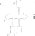
- FIG. 8 illustrates a typical processor system 700 including a processor and/or a memory device employing one or more of the thermal isolation structures and techniques described in connection with FIGS. 3-7 .
- Processor system 700 which may be, for example, a computer system, includes a central processing unit (CPU) 760, such as a microprocessor, a digital signal processor, or other programmable digital logic devices, which communicates with one or more input/output devices 780 over a bus 750.
- CPU central processing unit
- a memory device 770 also communicates with CPU 760 over bus 750, such as through a memory controller.
- the memory device 770 may include, for example, RAM, a hard drive, a FLASH drive or removable memory.
- processor system 700 may include other peripheral devices, such as removable media devices, that communicate with CPU 760 over bus 750.
- memory device 770 may be combined with CPU 760 as a single integrated circuit.
- Integrated circuits implementing the thermal isolation structures and techniques described herein may be used to provide efficient and reliable thermal isolation of photonic devices, electronic devices, and materials in one or more of CPU 760, memory device 770, input/output devices 780, or in connection with many other aspects of a processor system 700.
Claims (20)
- Structure intégrée comprenant :un substrat ayant une surface supérieure ;une première tranchée formée dans la surface supérieure du substrat ;une région de formation de dispositif au-dessus de la surface supérieure du substrat ;un dispositif photonique sensible à la température formé dans la région de formation de dispositif ;un dispositif de chauffage formé dans la région de formation de dispositif pour chauffer le premier dispositif photonique sensible à la température, le dispositif de chauffage étant situé au-dessus de la première tranchée ; etune première région d'isolation thermique formée sous le dispositif de chauffage, la première région d'isolation thermique étant située dans la première tranchée, de sorte que la première région d'isolation thermique est disposée dans la surface supérieure du substrat, et la première région d'isolation thermique réduisant la dissipation de la chaleur issue du dispositif de chauffage dans le substrat.
- Structure intégrée de la revendication 1, dans laquelle la région d'isolation thermique est formée dans une zone du substrat sous le dispositif de chauffage et le dispositif photonique sensible à la température.
- Structure intégrée de la revendication 1, dans laquelle la région d'isolation thermique comprend un matériau de faible conductivité thermique.
- Structure intégrée de la revendication 3, dans laquelle le matériau de faible conductivité thermique comprend un oxyde dopé avec un matériau ayant une plus faible conductivité thermique que l'oxyde, du dioxyde de silicium poreux, ou du dioxyde de silicium déposé par rotation.
- Structure intégrée de la revendication 3, dans laquelle le matériau de faible conductivité thermique a une conductivité thermique qui est inférieure à environ 0,006 W/cm°C.
- Structure intégrée de la revendication 5, dans laquelle le dopant comprend du fluor.
- Structure intégrée de la revendication 1, dans laquelle le dispositif photonique sensible à la température comprend un modulateur d'onde porteuse.
- Structure intégrée de la revendication 2, dans laquelle la première tranchée et la première région d'isolation thermique sont formées sous la totalité du premier dispositif photonique sensible à la température.
- Structure intégrée de la revendication 8, comprenant en outre un deuxième dispositif photonique formé dans la région de formation de dispositif et dans laquelle la première tranchée et la première région d'isolation thermique sont formées sous le deuxième dispositif photonique.
- Structure intégrée de la revendication 1, comprenant en outre un deuxième dispositif photonique formé dans la région de formation de dispositif et comprenant en outre une deuxième tranchée disposée dans une surface supérieure du substrat et une deuxième région d'isolation thermique sous le deuxième dispositif photonique.
- Structure intégrée de la revendication 2, dans laquelle le substrat comprend un substrat de silicium massif et la première tranchée et la première région d'isolation thermique sont disposées dans une surface supérieure du silicium, ou bien le substrat comprend un substrat de silicium sur isolant et la première tranchée et la première région d'isolation thermique sont disposées dans l'isolant du substrat de silicium sur isolant.
- Structure intégrée de la revendication 2, dans laquelle la première tranchée et la première région d'isolation thermique forment une région d'isolation par tranchée peu profonde.
- Procédé de formation d'une structure intégrée, le procédé comprenant :l'obtention d'un substrat ayant une surface supérieure ;la formation d'une première tranchée dans la surface supérieure du substrat ;la formation d'un premier dispositif photonique sensible à la température au-dessus du substrat ;la formation d'un dispositif de chauffage au-dessus du substrat pour chauffer le premier dispositif photonique sensible à la température, le dispositif de chauffage étant situé au-dessus de la première tranchée ; etla formation d'une première région d'isolation thermique sous le dispositif de chauffage, la première région d'isolation thermique étant située dans la première tranchée, de sorte que la première région d'isolation thermique est disposée dans la surface supérieure du substrat, et la première région d'isolation thermique réduisant la dissipation de la chaleur issue du dispositif de chauffage dans le substrat dans la direction de la région d'isolation.
- Procédé de la revendication 13, dans lequel la formation de la première région d'isolation thermique comprend la formation d'une région de matériau de faible conductivité thermique qui est moins thermoconducteur que le matériau dans le substrat.
- Procédé de la revendication 14, dans lequel la formation de la région de matériau de faible conductivité thermique comprend :le dépôt du matériau de faible conductivité thermique dans la première tranchée.
- Procédé de la revendication 15, dans lequel le dépôt du matériau de faible conductivité thermique dans la tranchée comprend le dopage de dioxyde de silicium avec un matériau ayant une plus faible constante diélectrique que le dioxyde de silicium, le dépôt de dioxyde de silicium poreux, ou le dépôt de dioxyde de silicium au moyen d'un dépôt par rotation.
- Procédé de la revendication 13, dans lequel la formation d'une région de matériau de faible conductivité thermique comprend la formation d'une couche isolante entre le substrat et le dispositif de chauffage.
- Procédé de la revendication 17, dans lequel la couche isolante comprend un oxyde dopé avec un matériau ayant une plus faible conductivité thermique que l'oxyde, du dioxyde de silicium poreux, ou du dioxyde de silicium déposé par rotation.
- Procédé de la revendication 13, dans lequel la région d'isolation thermique est formée avant la formation du dispositif de chauffage, ou après la formation du dispositif de chauffage.
- Procédé de la revendication 13, dans lequel la région d'isolation thermique est formée après la formation du dispositif de chauffage, et comprenant en outre :la formation d'une ouverture près du dispositif de chauffage, l'ouverture passant dans le substrat ; et la formation de la région d'isolation thermique sous le dispositif de chauffage.
Applications Claiming Priority (2)
| Application Number | Priority Date | Filing Date | Title |
|---|---|---|---|
| US13/524,446 US9310552B2 (en) | 2012-06-15 | 2012-06-15 | Methods and apparatus providing thermal isolation of photonic devices |
| PCT/US2013/045421 WO2013188542A1 (fr) | 2012-06-15 | 2013-06-12 | Procédés et appareil assurant l'isolation thermique de dispositifs photoniques |
Publications (2)
| Publication Number | Publication Date |
|---|---|
| EP2862014A1 EP2862014A1 (fr) | 2015-04-22 |
| EP2862014B1 true EP2862014B1 (fr) | 2017-01-11 |
Family
ID=48741526
Family Applications (1)
| Application Number | Title | Priority Date | Filing Date |
|---|---|---|---|
| EP13733154.2A Active EP2862014B1 (fr) | 2012-06-15 | 2013-06-12 | Procédés et appareil assurant l'isolation thermique de dispositifs photoniques |
Country Status (7)
| Country | Link |
|---|---|
| US (4) | US9310552B2 (fr) |
| EP (1) | EP2862014B1 (fr) |
| JP (1) | JP6014756B2 (fr) |
| KR (1) | KR101688718B1 (fr) |
| CN (1) | CN104395797B (fr) |
| TW (1) | TWI496252B (fr) |
| WO (1) | WO2013188542A1 (fr) |
Families Citing this family (17)
| Publication number | Priority date | Publication date | Assignee | Title |
|---|---|---|---|---|
| US20060251785A1 (en) | 2005-05-06 | 2006-11-09 | Stefania Fraccon | Method for cooking food using steam |
| US9310552B2 (en) | 2012-06-15 | 2016-04-12 | Micron Technology, Inc. | Methods and apparatus providing thermal isolation of photonic devices |
| US9235065B1 (en) * | 2014-01-09 | 2016-01-12 | Sandia Corporation | Thermally tuneable optical modulator adapted for differential signaling |
| US9513497B2 (en) | 2014-02-05 | 2016-12-06 | Aurrion, Inc. | Opto-electronic modulator utilizing one or more heating elements |
| JP6667325B2 (ja) * | 2016-03-11 | 2020-03-18 | 古河電気工業株式会社 | 半導体光素子 |
| US11211305B2 (en) * | 2016-04-01 | 2021-12-28 | Texas Instruments Incorporated | Apparatus and method to support thermal management of semiconductor-based components |
| US10861796B2 (en) | 2016-05-10 | 2020-12-08 | Texas Instruments Incorporated | Floating die package |
| US10074639B2 (en) | 2016-12-30 | 2018-09-11 | Texas Instruments Incorporated | Isolator integrated circuits with package structure cavity and fabrication methods |
| JP6869830B2 (ja) | 2017-06-29 | 2021-05-12 | ルネサスエレクトロニクス株式会社 | 半導体装置およびその製造方法 |
| US10775559B2 (en) | 2018-01-26 | 2020-09-15 | Analog Photonics LLC | Photonics fabrication process performance improvement |
| US10976542B2 (en) | 2018-01-26 | 2021-04-13 | Analog Photonics LLC | Aberration correction of optical phased arrays |
| US10866359B2 (en) | 2018-01-30 | 2020-12-15 | Huawei Technologies Co., Ltd. | Apparatus and methods for accommodating manufacturing variance in optical photonic integrated circuits |
| GB2588313B (en) * | 2018-05-11 | 2022-10-05 | Rockley Photonics Ltd | Thermo-optical phase shift with ridged optical waveguide |
| CN109324368A (zh) * | 2018-08-15 | 2019-02-12 | 桂林电子科技大学 | 一种基于等离子体波导的逻辑输出光源 |
| US11042049B2 (en) * | 2019-10-09 | 2021-06-22 | Cisco Technology, Inc. | Thermal isolation element |
| US11226506B2 (en) * | 2020-03-17 | 2022-01-18 | Taiwan Semiconductor Manufacturing Company, Ltd. | Heater structure with a gas-filled isolation structure to improve thermal efficiency in a modulator device |
| US11906784B2 (en) | 2022-04-11 | 2024-02-20 | Nokia Solutions And Networks Oy | Turnable free space optical filters |
Family Cites Families (26)
| Publication number | Priority date | Publication date | Assignee | Title |
|---|---|---|---|---|
| DE4446101A1 (de) | 1994-12-22 | 1996-07-04 | Siemens Ag | Thermo-optischer Schalter mit verringertem Leistungsbedarf |
| DE4445835C2 (de) * | 1994-12-22 | 2000-01-13 | Bosch Gmbh Robert | Thermooptischer Schalter, insbesondere Richtkoppler, sowie Verfahren zu seiner Herstellung |
| JP3868122B2 (ja) | 1998-08-12 | 2007-01-17 | 日本電信電話株式会社 | 熱光学光変調器 |
| US20050269666A1 (en) * | 2004-06-07 | 2005-12-08 | Taiwan Semiconductor Manufacturing Company, Ltd. | Electrical fuses as programmable data storage |
| JP2000206476A (ja) | 1999-01-18 | 2000-07-28 | Kyocera Corp | 温度制御型光導波路 |
| WO2002024777A2 (fr) | 2000-09-22 | 2002-03-28 | Ppg Industries Ohio, Inc. | Procede de formation d'un revetement composite a enrobage double, revetement resultant et composition de revetement resistant a l'ecaillage |
| AUPR174300A0 (en) | 2000-11-28 | 2000-12-21 | Redfern Integrated Optics Pty Ltd | Thermo optical phase shifter with reduced power consumption |
| US6984581B2 (en) * | 2000-12-21 | 2006-01-10 | Intel Corporation | Structural reinforcement of highly porous low k dielectric films by ILD posts |
| JP2002194164A (ja) | 2000-12-27 | 2002-07-10 | Daikin Ind Ltd | 低誘電性の絶縁膜及びこれを使用した集積回路構造体 |
| US6870979B2 (en) * | 2002-10-09 | 2005-03-22 | The Furukawa Electric Co., Ltd | Optical circuit, method for manufacturing optical circuit, optical circuit device and method for controlling optical circuit device |
| US7034641B1 (en) | 2002-11-27 | 2006-04-25 | K2 Optronics, Inc. | Substrate structure for photonic assemblies and the like having a low-thermal-conductivity dielectric layer on a high-thermal-conductivity substrate body |
| US6983086B2 (en) | 2003-06-19 | 2006-01-03 | Intel Corporation | Thermally isolating optical devices |
| CN100430764C (zh) * | 2005-11-18 | 2008-11-05 | 中国科学院半导体研究所 | 一种基于soi的光子晶体分束器及制法 |
| EP1967876A4 (fr) | 2005-12-27 | 2013-04-17 | Ibiden Co Ltd | Carte de câblage composite optique et électrique et procédé de fabrication de celle-ci |
| KR100927594B1 (ko) | 2006-12-05 | 2009-11-23 | 한국전자통신연구원 | 평판형 광도파로(plc) 소자, 그 소자를 포함한 파장가변 광원 및 그 광원을 이용한 wdm-pon |
| WO2008111407A1 (fr) * | 2007-03-09 | 2008-09-18 | Nec Corporation | Déphaseur thermo-optique |
| US7947609B2 (en) | 2007-08-10 | 2011-05-24 | Tokyo Electron Limited | Method for etching low-k material using an oxide hard mask |
| WO2009051267A1 (fr) | 2007-10-18 | 2009-04-23 | Nec Corporation | Source de lumière à longueur d'onde variable |
| US7941014B1 (en) * | 2008-04-09 | 2011-05-10 | Sandia Corporation | Optical waveguide device with an adiabatically-varying width |
| US7920770B2 (en) | 2008-05-01 | 2011-04-05 | Massachusetts Institute Of Technology | Reduction of substrate optical leakage in integrated photonic circuits through localized substrate removal |
| US20110304412A1 (en) * | 2010-06-10 | 2011-12-15 | Hao Zhang | Acoustic Wave Resonators and Methods of Manufacturing Same |
| US10115654B2 (en) | 2010-06-18 | 2018-10-30 | Palo Alto Research Center Incorporated | Buried thermally conductive layers for heat extraction and shielding |
| CN101968577B (zh) * | 2010-09-17 | 2012-09-05 | 四川马尔斯科技有限责任公司 | 基于平面集成光子学的光学可调滤波器的调谐方法 |
| US8437585B2 (en) * | 2010-12-07 | 2013-05-07 | Intel Corporation | Low-cost passive optical waveguide using Si substrate |
| CN102051022A (zh) | 2010-12-09 | 2011-05-11 | 广东生益科技股份有限公司 | 环氧树脂组合物及使用其制作的半固化片与层压板 |
| US9310552B2 (en) | 2012-06-15 | 2016-04-12 | Micron Technology, Inc. | Methods and apparatus providing thermal isolation of photonic devices |
-
2012
- 2012-06-15 US US13/524,446 patent/US9310552B2/en active Active
-
2013
- 2013-06-12 EP EP13733154.2A patent/EP2862014B1/fr active Active
- 2013-06-12 CN CN201380031496.2A patent/CN104395797B/zh active Active
- 2013-06-12 WO PCT/US2013/045421 patent/WO2013188542A1/fr active Application Filing
- 2013-06-12 KR KR1020147036971A patent/KR101688718B1/ko active IP Right Grant
- 2013-06-12 JP JP2015517394A patent/JP6014756B2/ja active Active
- 2013-06-14 TW TW102121202A patent/TWI496252B/zh active
-
2016
- 2016-02-29 US US15/056,845 patent/US10090451B2/en active Active
-
2018
- 2018-08-20 US US16/105,755 patent/US10777722B2/en active Active
-
2020
- 2020-07-31 US US16/945,309 patent/US11217737B2/en active Active
Non-Patent Citations (1)
| Title |
|---|
| None * |
Also Published As
| Publication number | Publication date |
|---|---|
| US10090451B2 (en) | 2018-10-02 |
| EP2862014A1 (fr) | 2015-04-22 |
| KR20150018848A (ko) | 2015-02-24 |
| US20130336613A1 (en) | 2013-12-19 |
| KR101688718B1 (ko) | 2016-12-21 |
| JP2015519618A (ja) | 2015-07-09 |
| US11217737B2 (en) | 2022-01-04 |
| JP6014756B2 (ja) | 2016-10-25 |
| US20200365787A1 (en) | 2020-11-19 |
| TW201407727A (zh) | 2014-02-16 |
| US9310552B2 (en) | 2016-04-12 |
| US20190013452A1 (en) | 2019-01-10 |
| TWI496252B (zh) | 2015-08-11 |
| CN104395797B (zh) | 2018-08-24 |
| WO2013188542A1 (fr) | 2013-12-19 |
| US10777722B2 (en) | 2020-09-15 |
| US20160181495A1 (en) | 2016-06-23 |
| CN104395797A (zh) | 2015-03-04 |
Similar Documents
| Publication | Publication Date | Title |
|---|---|---|
| US11217737B2 (en) | Methods and apparatus providing thermal isolation of photonic devices | |
| US10197819B2 (en) | Efficient thermo-optic phase shifters using multi-pass heaters | |
| US9711534B2 (en) | Devices including a diamond layer | |
| KR101770886B1 (ko) | 실리콘-온-절연체 기판 상의 도파로의 광학 격리를 제공하는 방법 및 구조물 | |
| TWI480607B (zh) | 電子/光子積體電路架構及其製造方法 | |
| US10656442B2 (en) | Semiconductor device and method of manufacturing same | |
| US20150268417A1 (en) | Buried waveguide photodetector | |
| US10267989B2 (en) | Prestructured substrate for the production of photonic components, associated photonic circuit and manufacturing method | |
| WO2013032472A1 (fr) | Dérivation thermique | |
| KR102163885B1 (ko) | 전계흡수 광변조 소자 및 그 제조 방법 | |
| US20230003943A1 (en) | Manufacture of semiconductor device with optical transmission channel between optical coupler and outside of the semiconductor device | |
| Shubin et al. | Integration, processing and performance of low power thermally tunable CMOS-SOI WDM resonators | |
| US20120213467A1 (en) | Optical device with enhanced mechanical strength | |
| US20190293864A1 (en) | Frontend integration of electronics and photonics | |
| US10288813B2 (en) | Construction of integrated mode transformers | |
| CN111562687B (zh) | 制作半导体器件的方法、半导体器件和半导体集成电路 | |
| CN111580289A (zh) | 制作半导体器件的方法、半导体器件和半导体集成电路 |
Legal Events
| Date | Code | Title | Description |
|---|---|---|---|
| PUAI | Public reference made under article 153(3) epc to a published international application that has entered the european phase |
Free format text: ORIGINAL CODE: 0009012 |
|
| 17P | Request for examination filed |
Effective date: 20150115 |
|
| AK | Designated contracting states |
Kind code of ref document: A1 Designated state(s): AL AT BE BG CH CY CZ DE DK EE ES FI FR GB GR HR HU IE IS IT LI LT LU LV MC MK MT NL NO PL PT RO RS SE SI SK SM TR |
|
| AX | Request for extension of the european patent |
Extension state: BA ME |
|
| DAX | Request for extension of the european patent (deleted) | ||
| GRAP | Despatch of communication of intention to grant a patent |
Free format text: ORIGINAL CODE: EPIDOSNIGR1 |
|
| RIC1 | Information provided on ipc code assigned before grant |
Ipc: G02F 1/01 20060101ALI20160615BHEP Ipc: G02F 1/313 20060101AFI20160615BHEP Ipc: G02B 6/12 20060101ALI20160615BHEP |
|
| INTG | Intention to grant announced |
Effective date: 20160707 |
|
| GRAJ | Information related to disapproval of communication of intention to grant by the applicant or resumption of examination proceedings by the epo deleted |
Free format text: ORIGINAL CODE: EPIDOSDIGR1 |
|
| REG | Reference to a national code |
Ref country code: DE Ref legal event code: R079 Ref document number: 602013016466 Country of ref document: DE Free format text: PREVIOUS MAIN CLASS: G02B0006120000 Ipc: H01L0033640000 |
|
| GRAR | Information related to intention to grant a patent recorded |
Free format text: ORIGINAL CODE: EPIDOSNIGR71 |
|
| GRAS | Grant fee paid |
Free format text: ORIGINAL CODE: EPIDOSNIGR3 |
|
| GRAA | (expected) grant |
Free format text: ORIGINAL CODE: 0009210 |
|
| INTC | Intention to grant announced (deleted) | ||
| RIC1 | Information provided on ipc code assigned before grant |
Ipc: G02B 6/12 20060101ALI20161121BHEP Ipc: G02F 1/313 20060101ALI20161121BHEP Ipc: G02F 1/01 20060101ALI20161121BHEP Ipc: H01L 33/64 20100101AFI20161121BHEP |
|
| AK | Designated contracting states |
Kind code of ref document: B1 Designated state(s): AL AT BE BG CH CY CZ DE DK EE ES FI FR GB GR HR HU IE IS IT LI LT LU LV MC MK MT NL NO PL PT RO RS SE SI SK SM TR |
|
| INTG | Intention to grant announced |
Effective date: 20161206 |
|
| REG | Reference to a national code |
Ref country code: GB Ref legal event code: FG4D |
|
| REG | Reference to a national code |
Ref country code: CH Ref legal event code: EP |
|
| REG | Reference to a national code |
Ref country code: AT Ref legal event code: REF Ref document number: 861985 Country of ref document: AT Kind code of ref document: T Effective date: 20170115 |
|
| REG | Reference to a national code |
Ref country code: IE Ref legal event code: FG4D |
|
| REG | Reference to a national code |
Ref country code: DE Ref legal event code: R096 Ref document number: 602013016466 Country of ref document: DE |
|
| REG | Reference to a national code |
Ref country code: NL Ref legal event code: FP |
|
| REG | Reference to a national code |
Ref country code: LT Ref legal event code: MG4D |
|
| REG | Reference to a national code |
Ref country code: FR Ref legal event code: PLFP Year of fee payment: 5 |
|
| REG | Reference to a national code |
Ref country code: AT Ref legal event code: MK05 Ref document number: 861985 Country of ref document: AT Kind code of ref document: T Effective date: 20170111 |
|
| PG25 | Lapsed in a contracting state [announced via postgrant information from national office to epo] |
Ref country code: IS Free format text: LAPSE BECAUSE OF FAILURE TO SUBMIT A TRANSLATION OF THE DESCRIPTION OR TO PAY THE FEE WITHIN THE PRESCRIBED TIME-LIMIT Effective date: 20170511 Ref country code: NO Free format text: LAPSE BECAUSE OF FAILURE TO SUBMIT A TRANSLATION OF THE DESCRIPTION OR TO PAY THE FEE WITHIN THE PRESCRIBED TIME-LIMIT Effective date: 20170411 Ref country code: FI Free format text: LAPSE BECAUSE OF FAILURE TO SUBMIT A TRANSLATION OF THE DESCRIPTION OR TO PAY THE FEE WITHIN THE PRESCRIBED TIME-LIMIT Effective date: 20170111 Ref country code: GR Free format text: LAPSE BECAUSE OF FAILURE TO SUBMIT A TRANSLATION OF THE DESCRIPTION OR TO PAY THE FEE WITHIN THE PRESCRIBED TIME-LIMIT Effective date: 20170412 Ref country code: LT Free format text: LAPSE BECAUSE OF FAILURE TO SUBMIT A TRANSLATION OF THE DESCRIPTION OR TO PAY THE FEE WITHIN THE PRESCRIBED TIME-LIMIT Effective date: 20170111 Ref country code: HR Free format text: LAPSE BECAUSE OF FAILURE TO SUBMIT A TRANSLATION OF THE DESCRIPTION OR TO PAY THE FEE WITHIN THE PRESCRIBED TIME-LIMIT Effective date: 20170111 |
|
| PG25 | Lapsed in a contracting state [announced via postgrant information from national office to epo] |
Ref country code: RS Free format text: LAPSE BECAUSE OF FAILURE TO SUBMIT A TRANSLATION OF THE DESCRIPTION OR TO PAY THE FEE WITHIN THE PRESCRIBED TIME-LIMIT Effective date: 20170111 Ref country code: SE Free format text: LAPSE BECAUSE OF FAILURE TO SUBMIT A TRANSLATION OF THE DESCRIPTION OR TO PAY THE FEE WITHIN THE PRESCRIBED TIME-LIMIT Effective date: 20170111 Ref country code: PT Free format text: LAPSE BECAUSE OF FAILURE TO SUBMIT A TRANSLATION OF THE DESCRIPTION OR TO PAY THE FEE WITHIN THE PRESCRIBED TIME-LIMIT Effective date: 20170511 Ref country code: ES Free format text: LAPSE BECAUSE OF FAILURE TO SUBMIT A TRANSLATION OF THE DESCRIPTION OR TO PAY THE FEE WITHIN THE PRESCRIBED TIME-LIMIT Effective date: 20170111 Ref country code: BG Free format text: LAPSE BECAUSE OF FAILURE TO SUBMIT A TRANSLATION OF THE DESCRIPTION OR TO PAY THE FEE WITHIN THE PRESCRIBED TIME-LIMIT Effective date: 20170411 Ref country code: LV Free format text: LAPSE BECAUSE OF FAILURE TO SUBMIT A TRANSLATION OF THE DESCRIPTION OR TO PAY THE FEE WITHIN THE PRESCRIBED TIME-LIMIT Effective date: 20170111 Ref country code: PL Free format text: LAPSE BECAUSE OF FAILURE TO SUBMIT A TRANSLATION OF THE DESCRIPTION OR TO PAY THE FEE WITHIN THE PRESCRIBED TIME-LIMIT Effective date: 20170111 Ref country code: AT Free format text: LAPSE BECAUSE OF FAILURE TO SUBMIT A TRANSLATION OF THE DESCRIPTION OR TO PAY THE FEE WITHIN THE PRESCRIBED TIME-LIMIT Effective date: 20170111 |
|
| REG | Reference to a national code |
Ref country code: DE Ref legal event code: R097 Ref document number: 602013016466 Country of ref document: DE |
|
| PG25 | Lapsed in a contracting state [announced via postgrant information from national office to epo] |
Ref country code: SK Free format text: LAPSE BECAUSE OF FAILURE TO SUBMIT A TRANSLATION OF THE DESCRIPTION OR TO PAY THE FEE WITHIN THE PRESCRIBED TIME-LIMIT Effective date: 20170111 Ref country code: RO Free format text: LAPSE BECAUSE OF FAILURE TO SUBMIT A TRANSLATION OF THE DESCRIPTION OR TO PAY THE FEE WITHIN THE PRESCRIBED TIME-LIMIT Effective date: 20170111 Ref country code: CZ Free format text: LAPSE BECAUSE OF FAILURE TO SUBMIT A TRANSLATION OF THE DESCRIPTION OR TO PAY THE FEE WITHIN THE PRESCRIBED TIME-LIMIT Effective date: 20170111 Ref country code: EE Free format text: LAPSE BECAUSE OF FAILURE TO SUBMIT A TRANSLATION OF THE DESCRIPTION OR TO PAY THE FEE WITHIN THE PRESCRIBED TIME-LIMIT Effective date: 20170111 |
|
| PLBE | No opposition filed within time limit |
Free format text: ORIGINAL CODE: 0009261 |
|
| STAA | Information on the status of an ep patent application or granted ep patent |
Free format text: STATUS: NO OPPOSITION FILED WITHIN TIME LIMIT |
|
| PG25 | Lapsed in a contracting state [announced via postgrant information from national office to epo] |
Ref country code: SM Free format text: LAPSE BECAUSE OF FAILURE TO SUBMIT A TRANSLATION OF THE DESCRIPTION OR TO PAY THE FEE WITHIN THE PRESCRIBED TIME-LIMIT Effective date: 20170111 Ref country code: DK Free format text: LAPSE BECAUSE OF FAILURE TO SUBMIT A TRANSLATION OF THE DESCRIPTION OR TO PAY THE FEE WITHIN THE PRESCRIBED TIME-LIMIT Effective date: 20170111 |
|
| 26N | No opposition filed |
Effective date: 20171012 |
|
| PG25 | Lapsed in a contracting state [announced via postgrant information from national office to epo] |
Ref country code: MC Free format text: LAPSE BECAUSE OF FAILURE TO SUBMIT A TRANSLATION OF THE DESCRIPTION OR TO PAY THE FEE WITHIN THE PRESCRIBED TIME-LIMIT Effective date: 20170111 |
|
| REG | Reference to a national code |
Ref country code: CH Ref legal event code: PL |
|
| PG25 | Lapsed in a contracting state [announced via postgrant information from national office to epo] |
Ref country code: SI Free format text: LAPSE BECAUSE OF FAILURE TO SUBMIT A TRANSLATION OF THE DESCRIPTION OR TO PAY THE FEE WITHIN THE PRESCRIBED TIME-LIMIT Effective date: 20170111 |
|
| REG | Reference to a national code |
Ref country code: IE Ref legal event code: MM4A |
|
| PG25 | Lapsed in a contracting state [announced via postgrant information from national office to epo] |
Ref country code: LU Free format text: LAPSE BECAUSE OF NON-PAYMENT OF DUE FEES Effective date: 20170612 Ref country code: LI Free format text: LAPSE BECAUSE OF NON-PAYMENT OF DUE FEES Effective date: 20170630 Ref country code: CH Free format text: LAPSE BECAUSE OF NON-PAYMENT OF DUE FEES Effective date: 20170630 Ref country code: IE Free format text: LAPSE BECAUSE OF NON-PAYMENT OF DUE FEES Effective date: 20170612 |
|
| REG | Reference to a national code |
Ref country code: FR Ref legal event code: PLFP Year of fee payment: 6 |
|
| REG | Reference to a national code |
Ref country code: BE Ref legal event code: MM Effective date: 20170630 |
|
| PG25 | Lapsed in a contracting state [announced via postgrant information from national office to epo] |
Ref country code: BE Free format text: LAPSE BECAUSE OF NON-PAYMENT OF DUE FEES Effective date: 20170630 |
|
| PG25 | Lapsed in a contracting state [announced via postgrant information from national office to epo] |
Ref country code: MT Free format text: LAPSE BECAUSE OF NON-PAYMENT OF DUE FEES Effective date: 20170612 |
|
| PG25 | Lapsed in a contracting state [announced via postgrant information from national office to epo] |
Ref country code: HU Free format text: LAPSE BECAUSE OF FAILURE TO SUBMIT A TRANSLATION OF THE DESCRIPTION OR TO PAY THE FEE WITHIN THE PRESCRIBED TIME-LIMIT; INVALID AB INITIO Effective date: 20130612 |
|
| PG25 | Lapsed in a contracting state [announced via postgrant information from national office to epo] |
Ref country code: CY Free format text: LAPSE BECAUSE OF FAILURE TO SUBMIT A TRANSLATION OF THE DESCRIPTION OR TO PAY THE FEE WITHIN THE PRESCRIBED TIME-LIMIT Effective date: 20170111 |
|
| PG25 | Lapsed in a contracting state [announced via postgrant information from national office to epo] |
Ref country code: MK Free format text: LAPSE BECAUSE OF FAILURE TO SUBMIT A TRANSLATION OF THE DESCRIPTION OR TO PAY THE FEE WITHIN THE PRESCRIBED TIME-LIMIT Effective date: 20170111 |
|
| PG25 | Lapsed in a contracting state [announced via postgrant information from national office to epo] |
Ref country code: TR Free format text: LAPSE BECAUSE OF FAILURE TO SUBMIT A TRANSLATION OF THE DESCRIPTION OR TO PAY THE FEE WITHIN THE PRESCRIBED TIME-LIMIT Effective date: 20170111 |
|
| PG25 | Lapsed in a contracting state [announced via postgrant information from national office to epo] |
Ref country code: AL Free format text: LAPSE BECAUSE OF FAILURE TO SUBMIT A TRANSLATION OF THE DESCRIPTION OR TO PAY THE FEE WITHIN THE PRESCRIBED TIME-LIMIT Effective date: 20170111 |
|
| PGFP | Annual fee paid to national office [announced via postgrant information from national office to epo] |
Ref country code: NL Payment date: 20230626 Year of fee payment: 11 Ref country code: FR Payment date: 20230622 Year of fee payment: 11 Ref country code: DE Payment date: 20230627 Year of fee payment: 11 |
|
| PGFP | Annual fee paid to national office [announced via postgrant information from national office to epo] |
Ref country code: IT Payment date: 20230620 Year of fee payment: 11 Ref country code: GB Payment date: 20230620 Year of fee payment: 11 |