EP2858100A1 - Semiconductor module and production method for same - Google Patents
Semiconductor module and production method for same Download PDFInfo
- Publication number
- EP2858100A1 EP2858100A1 EP13797985.2A EP13797985A EP2858100A1 EP 2858100 A1 EP2858100 A1 EP 2858100A1 EP 13797985 A EP13797985 A EP 13797985A EP 2858100 A1 EP2858100 A1 EP 2858100A1
- Authority
- EP
- European Patent Office
- Prior art keywords
- source electrode
- copper connector
- bare
- semiconductor module
- gate electrode
- Prior art date
- Legal status (The legal status is an assumption and is not a legal conclusion. Google has not performed a legal analysis and makes no representation as to the accuracy of the status listed.)
- Granted
Links
Images






Classifications
-
- H—ELECTRICITY
- H10—SEMICONDUCTOR DEVICES; ELECTRIC SOLID-STATE DEVICES NOT OTHERWISE PROVIDED FOR
- H10D—INORGANIC ELECTRIC SEMICONDUCTOR DEVICES
- H10D30/00—Field-effect transistors [FET]
- H10D30/60—Insulated-gate field-effect transistors [IGFET]
-
- H—ELECTRICITY
- H10—SEMICONDUCTOR DEVICES; ELECTRIC SOLID-STATE DEVICES NOT OTHERWISE PROVIDED FOR
- H10W—GENERIC PACKAGES, INTERCONNECTIONS, CONNECTORS OR OTHER CONSTRUCTIONAL DETAILS OF DEVICES COVERED BY CLASS H10
- H10W99/00—Subject matter not provided for in other groups of this subclass
-
- H—ELECTRICITY
- H10—SEMICONDUCTOR DEVICES; ELECTRIC SOLID-STATE DEVICES NOT OTHERWISE PROVIDED FOR
- H10W—GENERIC PACKAGES, INTERCONNECTIONS, CONNECTORS OR OTHER CONSTRUCTIONAL DETAILS OF DEVICES COVERED BY CLASS H10
- H10W90/00—Package configurations
-
- H—ELECTRICITY
- H05—ELECTRIC TECHNIQUES NOT OTHERWISE PROVIDED FOR
- H05K—PRINTED CIRCUITS; CASINGS OR CONSTRUCTIONAL DETAILS OF ELECTRIC APPARATUS; MANUFACTURE OF ASSEMBLAGES OF ELECTRICAL COMPONENTS
- H05K1/00—Printed circuits
- H05K1/18—Printed circuits structurally associated with non-printed electric components
- H05K1/181—Printed circuits structurally associated with non-printed electric components associated with surface mounted components
-
- H—ELECTRICITY
- H05—ELECTRIC TECHNIQUES NOT OTHERWISE PROVIDED FOR
- H05K—PRINTED CIRCUITS; CASINGS OR CONSTRUCTIONAL DETAILS OF ELECTRIC APPARATUS; MANUFACTURE OF ASSEMBLAGES OF ELECTRICAL COMPONENTS
- H05K2201/00—Indexing scheme relating to printed circuits covered by H05K1/00
- H05K2201/10—Details of components or other objects attached to or integrated in a printed circuit board
- H05K2201/10007—Types of components
- H05K2201/10166—Transistor
-
- H—ELECTRICITY
- H05—ELECTRIC TECHNIQUES NOT OTHERWISE PROVIDED FOR
- H05K—PRINTED CIRCUITS; CASINGS OR CONSTRUCTIONAL DETAILS OF ELECTRIC APPARATUS; MANUFACTURE OF ASSEMBLAGES OF ELECTRICAL COMPONENTS
- H05K2201/00—Indexing scheme relating to printed circuits covered by H05K1/00
- H05K2201/10—Details of components or other objects attached to or integrated in a printed circuit board
- H05K2201/10227—Other objects, e.g. metallic pieces
- H05K2201/1031—Surface mounted metallic connector elements
-
- H—ELECTRICITY
- H05—ELECTRIC TECHNIQUES NOT OTHERWISE PROVIDED FOR
- H05K—PRINTED CIRCUITS; CASINGS OR CONSTRUCTIONAL DETAILS OF ELECTRIC APPARATUS; MANUFACTURE OF ASSEMBLAGES OF ELECTRICAL COMPONENTS
- H05K2201/00—Indexing scheme relating to printed circuits covered by H05K1/00
- H05K2201/10—Details of components or other objects attached to or integrated in a printed circuit board
- H05K2201/10227—Other objects, e.g. metallic pieces
- H05K2201/10409—Screws
-
- H—ELECTRICITY
- H10—SEMICONDUCTOR DEVICES; ELECTRIC SOLID-STATE DEVICES NOT OTHERWISE PROVIDED FOR
- H10W—GENERIC PACKAGES, INTERCONNECTIONS, CONNECTORS OR OTHER CONSTRUCTIONAL DETAILS OF DEVICES COVERED BY CLASS H10
- H10W40/00—Arrangements for thermal protection or thermal control
- H10W40/20—Arrangements for cooling
- H10W40/25—Arrangements for cooling characterised by their materials
- H10W40/255—Arrangements for cooling characterised by their materials having a laminate or multilayered structure, e.g. direct bond copper [DBC] ceramic substrates
-
- H—ELECTRICITY
- H10—SEMICONDUCTOR DEVICES; ELECTRIC SOLID-STATE DEVICES NOT OTHERWISE PROVIDED FOR
- H10W—GENERIC PACKAGES, INTERCONNECTIONS, CONNECTORS OR OTHER CONSTRUCTIONAL DETAILS OF DEVICES COVERED BY CLASS H10
- H10W72/00—Interconnections or connectors in packages
- H10W72/01—Manufacture or treatment
- H10W72/015—Manufacture or treatment of bond wires
- H10W72/01565—Thermally treating
-
- H—ELECTRICITY
- H10—SEMICONDUCTOR DEVICES; ELECTRIC SOLID-STATE DEVICES NOT OTHERWISE PROVIDED FOR
- H10W—GENERIC PACKAGES, INTERCONNECTIONS, CONNECTORS OR OTHER CONSTRUCTIONAL DETAILS OF DEVICES COVERED BY CLASS H10
- H10W72/00—Interconnections or connectors in packages
- H10W72/01—Manufacture or treatment
- H10W72/016—Manufacture or treatment of strap connectors
-
- H—ELECTRICITY
- H10—SEMICONDUCTOR DEVICES; ELECTRIC SOLID-STATE DEVICES NOT OTHERWISE PROVIDED FOR
- H10W—GENERIC PACKAGES, INTERCONNECTIONS, CONNECTORS OR OTHER CONSTRUCTIONAL DETAILS OF DEVICES COVERED BY CLASS H10
- H10W72/00—Interconnections or connectors in packages
- H10W72/01—Manufacture or treatment
- H10W72/016—Manufacture or treatment of strap connectors
- H10W72/01661—Chemical or physical modification, e.g. by sintering or anodisation
-
- H—ELECTRICITY
- H10—SEMICONDUCTOR DEVICES; ELECTRIC SOLID-STATE DEVICES NOT OTHERWISE PROVIDED FOR
- H10W—GENERIC PACKAGES, INTERCONNECTIONS, CONNECTORS OR OTHER CONSTRUCTIONAL DETAILS OF DEVICES COVERED BY CLASS H10
- H10W72/00—Interconnections or connectors in packages
- H10W72/071—Connecting or disconnecting
- H10W72/0711—Apparatus therefor
- H10W72/07141—Means for applying energy, e.g. ovens or lasers
-
- H—ELECTRICITY
- H10—SEMICONDUCTOR DEVICES; ELECTRIC SOLID-STATE DEVICES NOT OTHERWISE PROVIDED FOR
- H10W—GENERIC PACKAGES, INTERCONNECTIONS, CONNECTORS OR OTHER CONSTRUCTIONAL DETAILS OF DEVICES COVERED BY CLASS H10
- H10W72/00—Interconnections or connectors in packages
- H10W72/071—Connecting or disconnecting
- H10W72/073—Connecting or disconnecting of die-attach connectors
-
- H—ELECTRICITY
- H10—SEMICONDUCTOR DEVICES; ELECTRIC SOLID-STATE DEVICES NOT OTHERWISE PROVIDED FOR
- H10W—GENERIC PACKAGES, INTERCONNECTIONS, CONNECTORS OR OTHER CONSTRUCTIONAL DETAILS OF DEVICES COVERED BY CLASS H10
- H10W72/00—Interconnections or connectors in packages
- H10W72/071—Connecting or disconnecting
- H10W72/073—Connecting or disconnecting of die-attach connectors
- H10W72/07331—Connecting techniques
- H10W72/07334—Using a reflow oven
-
- H—ELECTRICITY
- H10—SEMICONDUCTOR DEVICES; ELECTRIC SOLID-STATE DEVICES NOT OTHERWISE PROVIDED FOR
- H10W—GENERIC PACKAGES, INTERCONNECTIONS, CONNECTORS OR OTHER CONSTRUCTIONAL DETAILS OF DEVICES COVERED BY CLASS H10
- H10W72/00—Interconnections or connectors in packages
- H10W72/071—Connecting or disconnecting
- H10W72/073—Connecting or disconnecting of die-attach connectors
- H10W72/07331—Connecting techniques
- H10W72/07336—Soldering or alloying
-
- H—ELECTRICITY
- H10—SEMICONDUCTOR DEVICES; ELECTRIC SOLID-STATE DEVICES NOT OTHERWISE PROVIDED FOR
- H10W—GENERIC PACKAGES, INTERCONNECTIONS, CONNECTORS OR OTHER CONSTRUCTIONAL DETAILS OF DEVICES COVERED BY CLASS H10
- H10W72/00—Interconnections or connectors in packages
- H10W72/071—Connecting or disconnecting
- H10W72/073—Connecting or disconnecting of die-attach connectors
- H10W72/07351—Connecting or disconnecting of die-attach connectors characterised by changes in properties of the die-attach connectors during connecting
- H10W72/07354—Connecting or disconnecting of die-attach connectors characterised by changes in properties of the die-attach connectors during connecting changes in dispositions
-
- H—ELECTRICITY
- H10—SEMICONDUCTOR DEVICES; ELECTRIC SOLID-STATE DEVICES NOT OTHERWISE PROVIDED FOR
- H10W—GENERIC PACKAGES, INTERCONNECTIONS, CONNECTORS OR OTHER CONSTRUCTIONAL DETAILS OF DEVICES COVERED BY CLASS H10
- H10W72/00—Interconnections or connectors in packages
- H10W72/071—Connecting or disconnecting
- H10W72/075—Connecting or disconnecting of bond wires
-
- H—ELECTRICITY
- H10—SEMICONDUCTOR DEVICES; ELECTRIC SOLID-STATE DEVICES NOT OTHERWISE PROVIDED FOR
- H10W—GENERIC PACKAGES, INTERCONNECTIONS, CONNECTORS OR OTHER CONSTRUCTIONAL DETAILS OF DEVICES COVERED BY CLASS H10
- H10W72/00—Interconnections or connectors in packages
- H10W72/071—Connecting or disconnecting
- H10W72/075—Connecting or disconnecting of bond wires
- H10W72/07531—Techniques
- H10W72/07536—Soldering or alloying
-
- H—ELECTRICITY
- H10—SEMICONDUCTOR DEVICES; ELECTRIC SOLID-STATE DEVICES NOT OTHERWISE PROVIDED FOR
- H10W—GENERIC PACKAGES, INTERCONNECTIONS, CONNECTORS OR OTHER CONSTRUCTIONAL DETAILS OF DEVICES COVERED BY CLASS H10
- H10W72/00—Interconnections or connectors in packages
- H10W72/071—Connecting or disconnecting
- H10W72/075—Connecting or disconnecting of bond wires
- H10W72/07551—Connecting or disconnecting of bond wires characterised by changes in properties of the bond wires during the connecting
-
- H—ELECTRICITY
- H10—SEMICONDUCTOR DEVICES; ELECTRIC SOLID-STATE DEVICES NOT OTHERWISE PROVIDED FOR
- H10W—GENERIC PACKAGES, INTERCONNECTIONS, CONNECTORS OR OTHER CONSTRUCTIONAL DETAILS OF DEVICES COVERED BY CLASS H10
- H10W72/00—Interconnections or connectors in packages
- H10W72/071—Connecting or disconnecting
- H10W72/076—Connecting or disconnecting of strap connectors
-
- H—ELECTRICITY
- H10—SEMICONDUCTOR DEVICES; ELECTRIC SOLID-STATE DEVICES NOT OTHERWISE PROVIDED FOR
- H10W—GENERIC PACKAGES, INTERCONNECTIONS, CONNECTORS OR OTHER CONSTRUCTIONAL DETAILS OF DEVICES COVERED BY CLASS H10
- H10W72/00—Interconnections or connectors in packages
- H10W72/071—Connecting or disconnecting
- H10W72/076—Connecting or disconnecting of strap connectors
- H10W72/07631—Techniques
- H10W72/07636—Soldering or alloying
-
- H—ELECTRICITY
- H10—SEMICONDUCTOR DEVICES; ELECTRIC SOLID-STATE DEVICES NOT OTHERWISE PROVIDED FOR
- H10W—GENERIC PACKAGES, INTERCONNECTIONS, CONNECTORS OR OTHER CONSTRUCTIONAL DETAILS OF DEVICES COVERED BY CLASS H10
- H10W72/00—Interconnections or connectors in packages
- H10W72/071—Connecting or disconnecting
- H10W72/076—Connecting or disconnecting of strap connectors
- H10W72/07651—Connecting or disconnecting of strap connectors characterised by changes in properties of the strap connectors during connecting
- H10W72/07652—Connecting or disconnecting of strap connectors characterised by changes in properties of the strap connectors during connecting changes in structures or sizes
-
- H—ELECTRICITY
- H10—SEMICONDUCTOR DEVICES; ELECTRIC SOLID-STATE DEVICES NOT OTHERWISE PROVIDED FOR
- H10W—GENERIC PACKAGES, INTERCONNECTIONS, CONNECTORS OR OTHER CONSTRUCTIONAL DETAILS OF DEVICES COVERED BY CLASS H10
- H10W72/00—Interconnections or connectors in packages
- H10W72/071—Connecting or disconnecting
- H10W72/076—Connecting or disconnecting of strap connectors
- H10W72/07651—Connecting or disconnecting of strap connectors characterised by changes in properties of the strap connectors during connecting
- H10W72/07653—Connecting or disconnecting of strap connectors characterised by changes in properties of the strap connectors during connecting changes in shapes
-
- H—ELECTRICITY
- H10—SEMICONDUCTOR DEVICES; ELECTRIC SOLID-STATE DEVICES NOT OTHERWISE PROVIDED FOR
- H10W—GENERIC PACKAGES, INTERCONNECTIONS, CONNECTORS OR OTHER CONSTRUCTIONAL DETAILS OF DEVICES COVERED BY CLASS H10
- H10W72/00—Interconnections or connectors in packages
- H10W72/071—Connecting or disconnecting
- H10W72/076—Connecting or disconnecting of strap connectors
- H10W72/07651—Connecting or disconnecting of strap connectors characterised by changes in properties of the strap connectors during connecting
- H10W72/07654—Connecting or disconnecting of strap connectors characterised by changes in properties of the strap connectors during connecting changes in dispositions
-
- H—ELECTRICITY
- H10—SEMICONDUCTOR DEVICES; ELECTRIC SOLID-STATE DEVICES NOT OTHERWISE PROVIDED FOR
- H10W—GENERIC PACKAGES, INTERCONNECTIONS, CONNECTORS OR OTHER CONSTRUCTIONAL DETAILS OF DEVICES COVERED BY CLASS H10
- H10W72/00—Interconnections or connectors in packages
- H10W72/30—Die-attach connectors
- H10W72/321—Structures or relative sizes of die-attach connectors
- H10W72/325—Die-attach connectors having a filler embedded in a matrix
-
- H—ELECTRICITY
- H10—SEMICONDUCTOR DEVICES; ELECTRIC SOLID-STATE DEVICES NOT OTHERWISE PROVIDED FOR
- H10W—GENERIC PACKAGES, INTERCONNECTIONS, CONNECTORS OR OTHER CONSTRUCTIONAL DETAILS OF DEVICES COVERED BY CLASS H10
- H10W72/00—Interconnections or connectors in packages
- H10W72/30—Die-attach connectors
- H10W72/341—Dispositions of die-attach connectors, e.g. layouts
- H10W72/347—Dispositions of multiple die-attach connectors
-
- H—ELECTRICITY
- H10—SEMICONDUCTOR DEVICES; ELECTRIC SOLID-STATE DEVICES NOT OTHERWISE PROVIDED FOR
- H10W—GENERIC PACKAGES, INTERCONNECTIONS, CONNECTORS OR OTHER CONSTRUCTIONAL DETAILS OF DEVICES COVERED BY CLASS H10
- H10W72/00—Interconnections or connectors in packages
- H10W72/30—Die-attach connectors
- H10W72/351—Materials of die-attach connectors
- H10W72/352—Materials of die-attach connectors comprising metals or metalloids, e.g. solders
-
- H—ELECTRICITY
- H10—SEMICONDUCTOR DEVICES; ELECTRIC SOLID-STATE DEVICES NOT OTHERWISE PROVIDED FOR
- H10W—GENERIC PACKAGES, INTERCONNECTIONS, CONNECTORS OR OTHER CONSTRUCTIONAL DETAILS OF DEVICES COVERED BY CLASS H10
- H10W72/00—Interconnections or connectors in packages
- H10W72/30—Die-attach connectors
- H10W72/351—Materials of die-attach connectors
- H10W72/353—Materials of die-attach connectors not comprising solid metals or solid metalloids, e.g. ceramics
-
- H—ELECTRICITY
- H10—SEMICONDUCTOR DEVICES; ELECTRIC SOLID-STATE DEVICES NOT OTHERWISE PROVIDED FOR
- H10W—GENERIC PACKAGES, INTERCONNECTIONS, CONNECTORS OR OTHER CONSTRUCTIONAL DETAILS OF DEVICES COVERED BY CLASS H10
- H10W72/00—Interconnections or connectors in packages
- H10W72/50—Bond wires
-
- H—ELECTRICITY
- H10—SEMICONDUCTOR DEVICES; ELECTRIC SOLID-STATE DEVICES NOT OTHERWISE PROVIDED FOR
- H10W—GENERIC PACKAGES, INTERCONNECTIONS, CONNECTORS OR OTHER CONSTRUCTIONAL DETAILS OF DEVICES COVERED BY CLASS H10
- H10W72/00—Interconnections or connectors in packages
- H10W72/50—Bond wires
- H10W72/531—Shapes of wire connectors
- H10W72/5363—Shapes of wire connectors the connected ends being wedge-shaped
-
- H—ELECTRICITY
- H10—SEMICONDUCTOR DEVICES; ELECTRIC SOLID-STATE DEVICES NOT OTHERWISE PROVIDED FOR
- H10W—GENERIC PACKAGES, INTERCONNECTIONS, CONNECTORS OR OTHER CONSTRUCTIONAL DETAILS OF DEVICES COVERED BY CLASS H10
- H10W72/00—Interconnections or connectors in packages
- H10W72/50—Bond wires
- H10W72/551—Materials of bond wires
- H10W72/552—Materials of bond wires comprising metals or metalloids, e.g. silver
-
- H—ELECTRICITY
- H10—SEMICONDUCTOR DEVICES; ELECTRIC SOLID-STATE DEVICES NOT OTHERWISE PROVIDED FOR
- H10W—GENERIC PACKAGES, INTERCONNECTIONS, CONNECTORS OR OTHER CONSTRUCTIONAL DETAILS OF DEVICES COVERED BY CLASS H10
- H10W72/00—Interconnections or connectors in packages
- H10W72/60—Strap connectors, e.g. thick copper clips for grounding of power devices
- H10W72/621—Structures or relative sizes of strap connectors
- H10W72/627—Multiple strap connectors having different structures or shapes
-
- H—ELECTRICITY
- H10—SEMICONDUCTOR DEVICES; ELECTRIC SOLID-STATE DEVICES NOT OTHERWISE PROVIDED FOR
- H10W—GENERIC PACKAGES, INTERCONNECTIONS, CONNECTORS OR OTHER CONSTRUCTIONAL DETAILS OF DEVICES COVERED BY CLASS H10
- H10W72/00—Interconnections or connectors in packages
- H10W72/60—Strap connectors, e.g. thick copper clips for grounding of power devices
- H10W72/631—Shapes of strap connectors
-
- H—ELECTRICITY
- H10—SEMICONDUCTOR DEVICES; ELECTRIC SOLID-STATE DEVICES NOT OTHERWISE PROVIDED FOR
- H10W—GENERIC PACKAGES, INTERCONNECTIONS, CONNECTORS OR OTHER CONSTRUCTIONAL DETAILS OF DEVICES COVERED BY CLASS H10
- H10W72/00—Interconnections or connectors in packages
- H10W72/60—Strap connectors, e.g. thick copper clips for grounding of power devices
- H10W72/631—Shapes of strap connectors
- H10W72/634—Cross-sectional shape
-
- H—ELECTRICITY
- H10—SEMICONDUCTOR DEVICES; ELECTRIC SOLID-STATE DEVICES NOT OTHERWISE PROVIDED FOR
- H10W—GENERIC PACKAGES, INTERCONNECTIONS, CONNECTORS OR OTHER CONSTRUCTIONAL DETAILS OF DEVICES COVERED BY CLASS H10
- H10W72/00—Interconnections or connectors in packages
- H10W72/60—Strap connectors, e.g. thick copper clips for grounding of power devices
- H10W72/641—Dispositions of strap connectors
- H10W72/642—Dispositions of strap connectors being orthogonal to a side surface of the chip, e.g. in parallel arrangements
-
- H—ELECTRICITY
- H10—SEMICONDUCTOR DEVICES; ELECTRIC SOLID-STATE DEVICES NOT OTHERWISE PROVIDED FOR
- H10W—GENERIC PACKAGES, INTERCONNECTIONS, CONNECTORS OR OTHER CONSTRUCTIONAL DETAILS OF DEVICES COVERED BY CLASS H10
- H10W72/00—Interconnections or connectors in packages
- H10W72/60—Strap connectors, e.g. thick copper clips for grounding of power devices
- H10W72/641—Dispositions of strap connectors
- H10W72/646—Dispositions of strap connectors the connected ends being on auxiliary connecting means on bond pads, e.g. on a bump connector
-
- H—ELECTRICITY
- H10—SEMICONDUCTOR DEVICES; ELECTRIC SOLID-STATE DEVICES NOT OTHERWISE PROVIDED FOR
- H10W—GENERIC PACKAGES, INTERCONNECTIONS, CONNECTORS OR OTHER CONSTRUCTIONAL DETAILS OF DEVICES COVERED BY CLASS H10
- H10W72/00—Interconnections or connectors in packages
- H10W72/60—Strap connectors, e.g. thick copper clips for grounding of power devices
- H10W72/641—Dispositions of strap connectors
- H10W72/647—Dispositions of multiple strap connectors
-
- H—ELECTRICITY
- H10—SEMICONDUCTOR DEVICES; ELECTRIC SOLID-STATE DEVICES NOT OTHERWISE PROVIDED FOR
- H10W—GENERIC PACKAGES, INTERCONNECTIONS, CONNECTORS OR OTHER CONSTRUCTIONAL DETAILS OF DEVICES COVERED BY CLASS H10
- H10W72/00—Interconnections or connectors in packages
- H10W72/60—Strap connectors, e.g. thick copper clips for grounding of power devices
- H10W72/651—Materials of strap connectors
- H10W72/652—Materials of strap connectors comprising metals or metalloids, e.g. silver
-
- H—ELECTRICITY
- H10—SEMICONDUCTOR DEVICES; ELECTRIC SOLID-STATE DEVICES NOT OTHERWISE PROVIDED FOR
- H10W—GENERIC PACKAGES, INTERCONNECTIONS, CONNECTORS OR OTHER CONSTRUCTIONAL DETAILS OF DEVICES COVERED BY CLASS H10
- H10W72/00—Interconnections or connectors in packages
- H10W72/851—Dispositions of multiple connectors or interconnections
- H10W72/874—On different surfaces
- H10W72/884—Die-attach connectors and bond wires
-
- H—ELECTRICITY
- H10—SEMICONDUCTOR DEVICES; ELECTRIC SOLID-STATE DEVICES NOT OTHERWISE PROVIDED FOR
- H10W—GENERIC PACKAGES, INTERCONNECTIONS, CONNECTORS OR OTHER CONSTRUCTIONAL DETAILS OF DEVICES COVERED BY CLASS H10
- H10W72/00—Interconnections or connectors in packages
- H10W72/851—Dispositions of multiple connectors or interconnections
- H10W72/874—On different surfaces
- H10W72/886—Die-attach connectors and strap connectors
-
- H—ELECTRICITY
- H10—SEMICONDUCTOR DEVICES; ELECTRIC SOLID-STATE DEVICES NOT OTHERWISE PROVIDED FOR
- H10W—GENERIC PACKAGES, INTERCONNECTIONS, CONNECTORS OR OTHER CONSTRUCTIONAL DETAILS OF DEVICES COVERED BY CLASS H10
- H10W72/00—Interconnections or connectors in packages
- H10W72/90—Bond pads, in general
- H10W72/921—Structures or relative sizes of bond pads
- H10W72/926—Multiple bond pads having different sizes
-
- H—ELECTRICITY
- H10—SEMICONDUCTOR DEVICES; ELECTRIC SOLID-STATE DEVICES NOT OTHERWISE PROVIDED FOR
- H10W—GENERIC PACKAGES, INTERCONNECTIONS, CONNECTORS OR OTHER CONSTRUCTIONAL DETAILS OF DEVICES COVERED BY CLASS H10
- H10W72/00—Interconnections or connectors in packages
- H10W72/90—Bond pads, in general
- H10W72/931—Shapes of bond pads
- H10W72/932—Plan-view shape, i.e. in top view
-
- H—ELECTRICITY
- H10—SEMICONDUCTOR DEVICES; ELECTRIC SOLID-STATE DEVICES NOT OTHERWISE PROVIDED FOR
- H10W—GENERIC PACKAGES, INTERCONNECTIONS, CONNECTORS OR OTHER CONSTRUCTIONAL DETAILS OF DEVICES COVERED BY CLASS H10
- H10W72/00—Interconnections or connectors in packages
- H10W72/90—Bond pads, in general
- H10W72/951—Materials of bond pads
- H10W72/952—Materials of bond pads comprising metals or metalloids, e.g. PbSn, Ag or Cu
-
- H—ELECTRICITY
- H10—SEMICONDUCTOR DEVICES; ELECTRIC SOLID-STATE DEVICES NOT OTHERWISE PROVIDED FOR
- H10W—GENERIC PACKAGES, INTERCONNECTIONS, CONNECTORS OR OTHER CONSTRUCTIONAL DETAILS OF DEVICES COVERED BY CLASS H10
- H10W90/00—Package configurations
- H10W90/701—Package configurations characterised by the relative positions of pads or connectors relative to package parts
-
- H—ELECTRICITY
- H10—SEMICONDUCTOR DEVICES; ELECTRIC SOLID-STATE DEVICES NOT OTHERWISE PROVIDED FOR
- H10W—GENERIC PACKAGES, INTERCONNECTIONS, CONNECTORS OR OTHER CONSTRUCTIONAL DETAILS OF DEVICES COVERED BY CLASS H10
- H10W90/00—Package configurations
- H10W90/701—Package configurations characterised by the relative positions of pads or connectors relative to package parts
- H10W90/731—Package configurations characterised by the relative positions of pads or connectors relative to package parts of die-attach connectors
- H10W90/734—Package configurations characterised by the relative positions of pads or connectors relative to package parts of die-attach connectors between a chip and a stacked insulating package substrate, interposer or RDL
-
- H—ELECTRICITY
- H10—SEMICONDUCTOR DEVICES; ELECTRIC SOLID-STATE DEVICES NOT OTHERWISE PROVIDED FOR
- H10W—GENERIC PACKAGES, INTERCONNECTIONS, CONNECTORS OR OTHER CONSTRUCTIONAL DETAILS OF DEVICES COVERED BY CLASS H10
- H10W90/00—Package configurations
- H10W90/701—Package configurations characterised by the relative positions of pads or connectors relative to package parts
- H10W90/761—Package configurations characterised by the relative positions of pads or connectors relative to package parts of strap connectors
- H10W90/764—Package configurations characterised by the relative positions of pads or connectors relative to package parts of strap connectors between a chip and a stacked insulating package substrate, interposer or RDL
-
- Y—GENERAL TAGGING OF NEW TECHNOLOGICAL DEVELOPMENTS; GENERAL TAGGING OF CROSS-SECTIONAL TECHNOLOGIES SPANNING OVER SEVERAL SECTIONS OF THE IPC; TECHNICAL SUBJECTS COVERED BY FORMER USPC CROSS-REFERENCE ART COLLECTIONS [XRACs] AND DIGESTS
- Y02—TECHNOLOGIES OR APPLICATIONS FOR MITIGATION OR ADAPTATION AGAINST CLIMATE CHANGE
- Y02P—CLIMATE CHANGE MITIGATION TECHNOLOGIES IN THE PRODUCTION OR PROCESSING OF GOODS
- Y02P70/00—Climate change mitigation technologies in the production process for final industrial or consumer products
- Y02P70/50—Manufacturing or production processes characterised by the final manufactured product
Definitions
- the present invention relates to a semiconductor module such as a power module incorporated in an automotive electrical equipment, and a method for manufacturing the same.
- an electric power steering apparatus is provided with a motor driving unit in an enclosure accommodating an electric motor for steering of the automobile.
- the electronic apparatus is installed in the motor driving unit
- the electronic apparatus is incorporated as the power module in the motor driving unit.
- the power module is constituted as a so-called semiconductor module on which a power element such as a field effect transistor (FET) or insulated gate bipolar transistor (IGBT), for example, suitable for controlling an electrical equipment such as the electric power steering apparatus driven by relatively high current
- FET field effect transistor
- IGBT insulated gate bipolar transistor
- This kind of power module is also called “In-vehicle Module” since it is installed in a vehicle
- FIG. 14 is a cross-sectional schematic view of an example of a conventional semiconductor module.
- the semiconductor module 100 illustrated in FIG 14 is provided with: a substrate 101 made of metal; a resin 102 provided on a bottom flat surface of a recess portion of the substrate 101; and a plurality of copper foils (wiring patterns) 103a, 103b, 103c, and 103d formed on the resin 102. Grooves 109 are formed between the copper foil 103a and the copper foil 103d and between the copper foil 103c and the copper foil 103d. Then, thermal buffer plates 104a and 104b are formed on the copper foils 103a and 103b out of the plurality of copper foils 103a, 103b, 103c, and 103d, respectively. IGBTs 105a and 105b are formed on the buffer plates 104a and 104b, respectively. Each of the IGBTs 105a and 105b is a bare-chip IGBT (bare-chip transistor)
- the emitter of the IGBT 105a and the copper foil 103b are jointed to each other by a wiring 106a constituted of a wire
- the emitter of the IGBT 105b and the copper foil 103c are similarly jointed to each other by a wiring 106b constituted of a wire
- the resin 102, the copper foils 103a, 103b, and 103c, the buffer plates 104a and 104b, the IGBTs 105a and 105b, and the wirings 106a and 106b are sealed by a gel 107. Additionally, a cover 108 for covering the recess portion of the substrate 101 is fixed at an upper portion of the substrate 101.
- FIG. 15 is a plane schematic view of another example of the conventional semiconductor module
- the semiconductor module 200 illustrated in FIG. 15 is provided with a plurality of conductive pads 201 and 202 formed on a substrate (not illustrated). Then, a MOS chip 203 is connected by soldering on one conductive pad 201 out of the plurality of conductive pads 201 and 202. Additionally, a plurality of source electrodes 205 and a single gate electrode 204 are formed on the top surface of the MOS chip 203, and a drain electrode, not illustrated, is formed on the lower surface of the MOS chip 203.
- the lead 210 is formed by punching and bending a metal plate, and is provided with: a rectangular tabular source electrode jointing portion 211 extending in the X direction and Y direction (horizontal direction) illustrated in FIG.
- the source electrode jointing portion 211 is jointed by soldering with the source electrodes 205 of the MOS chip 203, and the electrode jointing portion 212 is jointed by soldering with the another conductive pad 202 out of the plurality of conductive pads 201 and 202.
- the width "a" of the source electrode jointing portion 211 in the X direction is equal to or longer than the width "b" of the plurality of source electrodes 205 in the X direction. This makes it possible to prevent non-uniform solder wetting on the source electrodes 205 and displacement of the source electrodes 205 due to the reflow of the solder.
- the emitter of the IGBT 105a and the copper foil 103b are jointed to each other by use of the wiring 106a constituted of a wire
- the emitter of the IGBT 105b and the copper foil 103c are jointed to each other by the wiring 106b constituted of a wire. Since the joint using a wire is achieved by use of a wire bonding apparatus (not illustrated), the mounting operation of the wirings 106a and 106b is different from the solder mounting operation for mounting the IGBTs 105a and 105b or the other surface mounting device on the wiring patterns on the substrate. This poses a problem that these operations need different manufacturing processes.
- the lead-out direction of the lead 210 jointed to the source electrodes 205 is only the Y direction illustrated in FIG. 15 .
- the lead jointed to the gate electrode 204 there is no description regarding the lead jointed to the gate electrode 204.
- the lead-out direction of the lead 210 jointed to the source electrodes 205 is only one direction, there is no flexibility of arranging the MOS chip 203 mounted on the substrate, and, there is no flexibility of design of wiring on the substrate. This lack of flexibility of design of wiring on the substrate poses a problem that the layout of the semiconductor module on the substrate cannot be compact.
- the present invention has been made to address the above conventional problems, and has an object to provide a semiconductor module and a method for manufacturing the same which make it possible to joint the electrode of the bare-chip transistor and the wiring pattern on the substrate by solder mounting operation, in the same process of solder mounting operation for mounting the bare-chip transistor or other surface mounting devices on the wiring patterns on the substrate.
- the present invention has another object to provide a semiconductor module and a method for manufacturing the same which make it possible to create flexibility of arranging the bare-chip transistor mounted on the substrate and flexibility of design of wiring on the substrate, to make the layout of the semiconductor module on the substrate compact, and in addition, which make it easy to uniform length of paths on the substrate for phases of a three-phase motor.
- a semiconductor module comprising: a substrate made of metal; an insulating layer formed on the substrate; a plurality of wiring patterns formed on the insulating layer; a bare-chip transistor mounted on one wiring pattern out of the plurality of wiring patterns via a solder; and a copper connector constituted of a copper plate for jointing an electrode formed on a top surface of the bare-chip transistor and another wiring pattern out of the plurality of wiring patterns via a solder.
- the electrode of the bare-chip transistor and the wiring pattern on the substrate can be jointed by solder mounting operation. Therefore, it is possible to joint the electrode of the bare-chip transistor and the wiring pattern on the substrate in the same process of solder mounting operation for mounting the bare-chip transistor or other surface mounting devices on the wiring patterns on the substrate.
- This allows to shorten the manufacturing takt time of the semiconductor module, and in addition, eliminates the need for the dedicated equipment for wire bonding, thereby reducing the manufacturing cost of the semiconductor module That is, it is possible to reduce investment in equipment since the equipment for solder mounting operation can be used for also jointing the electrode of the bare-chip transistor and the wiring pattern on the substrate.
- the copper plate may be a plate shaped member made of material having the same electrical characteristic and mechanical characteristic as those of copper
- the copper connector may be a connector made of material having the same electrical characteristic and mechanical characteristic as those of copper.
- the bare-chip transistor is preferably a bare-chip FET having a source electrode and a gate electrode formed on a top surface thereof
- the copper connector preferably includes a source electrode copper connector and a gate electrode copper connector
- the source electrode of the bare-chip FET and the another wiring pattern out of the plurality of wiring patterns are preferably jointed by the source electrode copper connector via a solder
- the gate electrode of the bare-chip FET and a further another wiring pattern out of the plurality of wiring patterns is preferably jointed by the gate electrode copper connector via a solder
- the source electrode of the bare-chip FET and the one wiring pattern on the substrate can be jointed by solder mounting operation by use of the source electrode copper connector, and the gate electrode of the bare-chip FET and the another wiring pattern on the substrate can be jointed by solder mounting operation by use of the gate electrode copper connector. Therefore, it is possible to make the joint between the source electrode of the bare-chip FET and the one wiring pattern on the substrate and the joint between the gate electrode of the bare-chip FET and the another wiring pattern on the substrate, in the same process of solder mounting operation for mounting the bare-chip FET or other surface mounting devices on the wiring patterns on the substrate.
- the gate electrode copper connector falls into one type
- the source electrode copper connector falls into two types including a first source electrode copper connector arranged 180 degrees straightly with respect to the gate electrode copper connector, and a second source electrode copper connector arranged 90 degrees perpendicularly with respect to the gate electrode copper connector
- the one type of the gate electrode copper connector and the source electrode copper connector selected from either of the two types including the first source electrode copper connector or the second source electrode copper connector are preferably used in combination with each other on one bare-chip FET.
- the gate electrode and the source electrode formed on the top surface of the bare-chip FET may be arranged straightly in series, and the source electrode may be formed to have a rectangle shape.
- the first source electrode copper connector is preferably led out in a direction that a short side of the source electrode extends, the source electrode being formed to have the rectangle shape with the short side and a long side, and preferably comprises a jointing portion having a short side and a long side corresponding to the short side and the long side of the source electrode, respectively, and an area of a joint surface of the jointing portion is preferably substantially equal to an area of the source electrode, the joint surface being jointed to the source electrode.
- the above semiconductor module it is possible to ensure the joint reliability between the source electrode formed on the top surface of the bare-chip FET and the first source electrode copper connector arranged 180 degrees straightly with respect to the gate electrode copper connector.
- the second source electrode copper connector is preferably led out in a direction that a long side of the source electrode extends, the source electrode being formed to have the rectangle shape with a short side and the long side, and preferably comprises a jointing portion having a long side and a short side corresponding to the long side and the short side of the source electrode, respectively, and an area of a joint surface of the jointing portion is preferably substantially equal to an area of the source electrode, the joint surface being jointed to the source electrode
- the above semiconductor module it is possible to ensure the joint reliability between the source electrode formed on the top surface of the bare-chip FET and the second source electrode copper connector arranged 90 degrees perpendicularly with respect to the gate electrode copper connector.
- a method for manufacturing a semiconductor module comprising the steps of: forming an insulating layer on a substrate made of metal; forming a plurality of wiring patterns on the insulating layer; applying solder paste on the plurality of wiring patterns; mounting a bare-chip transistor on the solder paste applied on one wiring pattern out of the plurality of wiring patterns; applying solder paste on an electrode formed on a top surface of the bare-chip transistor; configuring a semiconductor module intermediate assembly by mounting a copper connector constituted of a copper plate on the solder paste applied on the electrode of the bare-chip transistor and on the solder paste applied on another wiring pattern out of the plurality of wiring patterns; and putting the semiconductor module intermediate assembly in a reflow furnace to form a joint between the one wiring pattern out of the plurality of wiring patterns and the bare-chip transistor via a solder, a joint between the electrode formed on the top surface of the bare-chip transistor and the copper connector via a solder, and a joint
- the electrode of the bare-chip transistor and the wiring pattern on the substrate can be jointed by solder mounting operation. Therefore, it is possible to joint the electrode of the bare-chip transistor and the wiring pattern on the substrate in the same process of solder mounting operation for mounting the bare-chip transistor or other surface mounting devices on the wiring patterns on the substrate. This allows to shorten the manufacturing takt time of the semiconductor module, and in addition, eliminates the need for the dedicated equipment for wire bonding, thereby reducing the manufacturing cost of the semiconductor module.
- the bare-chip transistor is preferably a bare-chip FET having a source electrode and a gate electrode formed on a top surface thereof
- the copper connector preferably includes a source electrode copper connector and a gate electrode copper connector
- the method preferably comprises the steps of: forming the insulating layer on the substrate made of metal; forming the plurality of wiring patterns on the insulating layer; applying the solder paste on the plurality of wiring patterns; mounting the bare-chip FET on the solder paste applied on the one wiring pattern out of the plurality of wiring patterns; applying solder paste on the source electrode and the gate electrode formed on the top surface of the bare-chip FET; mounting the source electrode copper connector on the solder paste applied on the source electrode of the bare-chip FET and on the solder paste applied on the another wiring pattern out of the plurality of wiring patterns; configuring the semiconductor module intermediate assembly by mounting the gate electrode copper connector on the solder paste applied on the gate electrode of the bare-chip FET and on the
- the source electrode of the bare-chip FET and the one wiring pattern on the substrate can be jointed by solder mounting operation by use of the source electrode copper connector, and the gate electrode of the bare-chip FET and the another wiring pattern on the substrate can be jointed by solder mounting operation by use of the gate electrode copper connector. Therefore, it is possible to make the joint between the source electrode of the bare-chip FET and the one wiring pattern on the substrate and the joint between the gate electrode of the bare-chip FET and the another wiring pattern on the substrate, in the same process of solder mounting operation for mounting the bare-chip FET or other surface mounting devices on the wiring patterns on the substrate.
- the gate electrode copper connector falls into one type
- the source electrode copper connector falls into two types including a first source electrode copper connector arranged 180 degrees straightly with respect to the gate electrode copper connector, and a second source electrode copper connector arranged 90 degrees perpendicularly with respect to the gate electrode copper connector
- the one type of the gate electrode copper connector and the source electrode copper connector selected from either of the two types including the first source electrode copper connector or the second source electrode copper connector are preferably used in combination with each other on one bare-chip FET.
- a semiconductor module comprising a joint between an electrode of a bare-chip transistor and a wiring pattern on a substrate made by solder mounting operation by use of a copper connector constituted of copper.
- a semiconductor module characterized in that one type of gate electrode copper connector and a source electrode copper connector selected from either of two types including a first source electrode copper connector arranged 180 degrees straightly with respect to the gate electrode copper connector or a second source electrode copper connector arranged 90 degrees perpendicularly with respect to the gate electrode copper connector are used in combination with each other on one bare-chip FET, such that flexibility of arranging a bare-chip transistor mounted on a substrate is created, and flexibility of design of wiring on the substrate is increased, thus layout of the semiconductor module on the substrate can be compact.
- the electrode of the bare-chip transistor and the wiring pattern on the substrate can be jointed by solder mounting operation Therefore, it is possible to joint the electrode of the bare-chip transistor and the wiring pattern on the substrate in the same process of solder mounting operation for mounting the bare-chip transistor or other surface mounting devices on the wiring patterns on the substrate. This allows to shorten the manufacturing takt time of the semiconductor module, and in addition, eliminates the need for the dedicated equipment for wire bonding, thereby reducing the manufacturing cost of the semiconductor module..
- the semiconductor module and the above method of manufacturing the semiconductor module when using the one type of the gate electrode copper connector and the source electrode copper connector selected from either of the two types including the first source electrode copper connector or the second source electrode copper connector in combination with each other on one bare-chip FET, flexibility of arranging the bare-chip transistor mounted on the substrate is created and flexibility of design of wiring on the substrate is increased, thus the layout of the semiconductor module on the substrate can be compact.
- FIG. 1 is a view illustrating a basic structure of an electric power steering apparatus using a semiconductor module according to the present invention.
- FIG. 2 is a block diagram illustrating a control system of a controller of the electric power steering apparatus illustrated in FIG 1 .
- FIG. 3 is an exploded perspective view of the controller including the semiconductor module of the electric power steering apparatus illustrated in FIG. 1 .
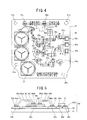
- FIG. 4 is a plane view of the semiconductor module illustrated in FIG. 3
- FIG 5 is a schematic view illustrating the joint state between the wiring pattern on the substrate and the electrode of the bare-chip FET constituting the bare-chip transistor in the semiconductor module illustrated in FIG. 3 and FIG. 4 .
- FIG. 1 is a view illustrating a basic structure of an electric power steering apparatus using a semiconductor module according to the present invention.
- FIG. 2 is a block diagram illustrating a control system of a controller of the electric power steering apparatus illustrated in FIG 1 .
- FIG. 3 is an exploded perspective view of the controller including the semiconductor module of the electric power steering
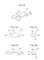
- FIG. 6A is a plane view illustrating the joint state between the electrode of the bare-chip FET and the copper connector, in the case where the gate electrode copper connector is jointed to the gate electrode of the bare-chip FET as well as the first source electrode copper connector is jointed to the source electrode.
- FIG 6B is a plane view illustrating the connection state between the electrode of the bare-chip FET and the copper connector, in the case where the gate electrode copper connector is jointed to the gate electrode of the bare-chip FET as well as the second source electrode copper connector is jointed to the source electrode.
- FIG. 7 is a schematic plan view of the bare-chip FET.
- FIG. 1 a basic structure of an electric power steering apparatus using a semiconductor module according to the present invention is illustrated
- a column shaft 2 of a steering wheel 1 is connected to tie rod 6 of a steered wheel through a speed reducing gears 3, universal joints 4A and 4B, and a rack and pinion mechanism 5.
- the column shaft 2 is provided with a torque sensor 7 for detecting the steering torque of the steering wheel 1, an electric motor 8 for assisting the steering force of the steering wheel 1 is connected to the column shaft 2 through the speed reduction gears 3
- Electric power is supplied from a battery, not illustrated, to a controller 10 for controlling the electric power steering apparatus and an ignition key signal IGN (see FIG. 2 ) is inputted into the controller 10 through an ignition key, not illustrated.
- IGN ignition key signal
- the controller 10 calculates a steering assisting command value as an assist (steering assisting) command base on a steering torque Ts detected by the torque sensor 7 and a vehicle velocity V detected by a vehicle velocity sensor 9, and controls a current supplied to the electric motor 8 based on the calculated steering assisting command value.
- the controller 10 is mainly constituted of a micro computer, and the mechanism and configuration of the controlling apparatus are illustrated in FIG. 2 .
- the steering torque Ts detected by the torque sensor 7 and the vehicle velocity V detected by the vehicle velocity sensor 9 are inputted to a control calculation device 11 as a control calculation unit, and a current command value calculated by the control calculation device 11 is inputted to a gate driving circuit 12.
- a gate driving signal formed by the gate driving circuit 12 based on the current command value is inputted to a motor driving unit 13 including a bridge configuration of FETs.
- the motor driving unit 13 drives the electric motor 8 constituted of a three-phase brushless motor, through a breaker device 14 for emergency stop Each of phase currents of the three-phase brushless motor is detected by a current detecting circuit 15.
- the detected three-phase motor currents ia to ic are inputted to the control calculation device 11 as feedback currents
- the three-phase brushless motor is equipped with a rotation sensor 16 such as a Hall sensor, a rotation signal RT from the rotation sensor 16 is inputted to a rotor position detecting circuit 17, and the detected rotation position ⁇ is inputted to the control calculation device 11.
- the ignition signal IGN from the ignition key is inputted into an ignition voltage monitor unit 18 and a power supply circuit unit 19.
- Power supply voltage Vdd from the power supply circuit unit 19 is inputted to the control calculation device 11, and a reset signal Rs for stopping the apparatus is inputted to the control calculation device 11.
- the breaker device 14 is constituted of relay contacts 141 and 142 for breaking two phases.
- a serial connection of FETs Tr1 and Tr2, a serial connection of FETs Tr3 and Tr4, and a serial connection of FETs Tr5 and Tr6 are connected to a power-supply line 81, in such a manner that these serial connections are connected in parallel with one another.
- the serial connection of FETs Tr1 and Tr2, the serial connection of FETs Tr3 and Tr4, and the serial connection of FETs Tr5 and Tr6, which are connected to the power-supply line 81 in such a manner that these serial connections are connected in parallel with one another, are connected a ground line 82.
- Such a configuration constitutes an inverter.
- the source electrode S of the FET Tr1 and the drain electrode D of the FET Tr2 are connected in series, and the FFTs Tr1 and Tr2 constitute a c-phase arm of the three-phase motor and output a current at a c-phase output line 91c.
- the source electrode S of the FET Tr3 and the drain electrode D of the FET Tr4 are connected in series, and the FFTs Tr3 and Tr4 constitute an a-phase arm of the three-phase motor and output a current at an a-phase output line 91a.
- the source electrode S of the FET Tr5 and the drain electrode D of the FET Tr6 are connected in series, and the FFTs Tr5 and Tr6 constitute a b-phase arm of the three-phase motor and output b current at a b-phase output line 91b
- FIG. 3 is an exploded perspective view of the controller 10 including the semiconductor module of the electric power steering apparatus illustrated in FIG 1 .
- the controller 10 is provided with: a case 20; a semiconductor module 30 as a power module including the motor driving unit 13; a heat dissipation sheet 39; a control circuit substrate 40 including the control calculation device 11 and the gate driving circuit 12; a power/signal connector 50; a three-phase output connector 60; and a cover 70.
- the case 20 is formed to have a substantially rectangular shape, and provided with a tabular semiconductor module placement portion 21 on which the semiconductor module 30 is placed; and a power/signal connector mounting portion 22 arranged on an end part in a length direction of the semiconductor module placement portion 21, on which the power/signal connector 50 is mounted; and a three-phase output connector mounting portion 23 arranged on an end part in a width direction of the semiconductor module placement portion 21, on which the three-phase output connector 60 is mounted.
- a plurality of screw holes 21a are formed on the semiconductor module placement portion 21, and an attachment screw 38 for attaching the semiconductor module 30 is screwed into the screw hole 21a
- the semiconductor module placement portion 21 and the power/signal connector mounting portion 22 are provided with a plurality of attaching posts 24 vertically standing for attaching the control circuit substrate 40.
- Screw holes 24a are formed on the attaching post 24, and an attachment screw 41 for attaching the control circuit substrate 40 is screwed into the screw hole 24a.
- a plurality of screw holes 23a are formed on the three-phase output connector mounting portion 23, and an attachment screw 61 for attaching the three-phase output connector 60 is screwed into the screw hole 23a.
- the semiconductor module 30 is provided with the circuit configuration of the motor driving unit 13 described above.
- the six FETs Tr1 to Tr6 a positive electrode terminal 81a connected to the power-supply line 81, and a negative electrode terminal 82a connected to the ground line 82, are mounted on a substrate 31.
- a three-phase output portion 90 including an a-phase output terminal 92a connected to the a-phase output line 91a, a b-phase output terminal 92b connected to the b-phase output line 91b, and a c-phase output terminal 92c connected to the c-phase output line 91c, are mounted on the substrate 31.
- Each of the FTTs Tr1 to Tr6 is constituted of a bare-chip FET (bare-chip transistor) 35, and is provided with a source electrode S and a gate electrode G on the bare-chip FET 35, as illustrated in FIG. 7 , and is provided with a drain electrode, not illustrated, on the lower surface of the bare-chip FET 35.
- bare-chip FET bare-chip transistor
- the gate electrode G and source electrode S formed on the top surface of the bare-chip FET 35 are arranged straightly in series in up-down direction of FIG. 7 , as illustrated in FIG. 7 .
- the gate electrode G is formed to have a rectangle shape, the short side thereof extending in up-down direction of FIG. 7 , and the long side thereof being orthogonal to the short side.
- the gate electrode S is formed to have a rectangle shape, the short side thereof extending in up-down direction of FIG.. 7 , and the long side thereof being orthogonal to the short side.
- the short side and the long side of the source electrode S is longer than the short side and the long side of the gate electrode G, and the area of the source electrode S is lager than the area of the gate electrode G.
- the semiconductor module 30 is provided with the substrate 31 made of metal as illustrated in FIG. 5 , and an insulating layer 32 is formed on the substrate 31.
- the substrate 31 is made of metal such as aluminum.
- a plurality of wiring patterns 33a to 33d are formed on the insulating layer 32.
- Each of the wiring patterns 33a to 33d are constituted of metal such as copper or aluminum, or alloy containing these kinds of metal.
- the bare-chip FET 35 constituting each of the FETs Tr1 to Tr6 is mounted on one wiring pattern 33a out of the plurality of wiring patterns 33a to 33d via a solder 34a.
- the drain electrode formed on the lower surface of the bare-chip FET 35 is jointed to the wiring pattern 33a via the solder 34a Then, the top of the source electrode S of the bare-chip FET 35 and the top of another wiring pattern 33b out of the plurality of wiring patterns 33a to 33d are jointed by a source electrode copper connector 36a via solders 34e, 34b. In addition, the top of the gate electrode G of the bare-chip FET 35 and the top of a further another wiring pattern 33c out of the plurality of wiring patterns 33a to 33d are jointed by a gate electrode copper connector 36b via solders 34f, 34c.
- source electrode copper connectors 36a constituted of a first source electrode copper connector 36a1 arranged 180 degrees straightly with respect to the gate electrode copper connector 36b as illustrated in FIG. 6A , and a second source electrode copper connector 36a2 arranged 90 degrees perpendicularly with respect to the gate electrode copper connector 36b as illustrated in FIG 6B .
- the first source electrode copper connector 36a1 is jointed and led out in a direction of an arrow A' illustrated in FIG. 7
- the second source electrode copper connector 36a2 is jointed and led out in a direction of an arrow B illustrated in FIG. 7 .
- the second source electrode copper connector 36a2 is jointed and led out in a direction of an arrow B' illustrated in FIG. 7 .
- the one type of the gate electrode copper connector 36b and the source electrode copper connector selected from either of two types including the first source electrode copper connector 36a1 or the second source electrode copper connector 36a2 are used in combination with each other on one bare-chip FET 35.
- the gate electrode copper connector 36b is formed by punching and bending a copper plate, and is provided with: a flat plate portion 36ba; a jointing portion 36bb extending from one end of the flat plate portion 36ba and jointed to the gate electrode G of the bare-chip FET 35 via the solder 34f; and a jointing portion .36bc extending from another end of the flat plate portion 36ba and jointed to the wiring pattern 33c via the solder 34c.
- the flat plate portion ba of the gate electrode copper connector 36b constitutes a suction surface sucked by a sucker apparatus using air. This allows suction using air through the use of the flat plate portion ba.
- the jointing portion 36bb of the gate electrode copper connector 36b is formed at the lower end of a coupling piece 36bd extending obliquely downward from one end of the flat plate portion 36ba, and extending outward
- the jointing portion 36bb has a short side and a long side along the short side and the long side of the gate electrode G, and the area of the joint surface thereof jointing to the gate electrode G is substantially equal to the area of the gate electrode G Since the area of the joint surface of the jointing portion 36bb jointing to the gate electrode G is substantially equal to the area of the gate electrode G, it is possible to ensure the joint reliability between the gate electrode copper connector 36b and the gate electrode G.
- the jointing portion 36bc of the gate electrode copper connector 36b is formed at the lower end of a coupling piece 36be extending obliquely downward from another end of the flat plate portion 36ba, and extending outward.
- the jointing portion 36bc locates lower then the jointing portion 36bb.
- the area of the joint surface of the jointing portion 36bc jointing to the wiring pattern 33c is larger than the area of the joint surface of the jointing portion 36bb connecting to the gate electrode G.
- the gate electrode copper connector 36b is formed to have a substantially lateral U shape when viewed from the front, having the flat plate portion 36ba, the coupling piece 36bd, the jointing portion 36bb, the coupling piece 36be and the jointing portion 36bc, as illustrated in FIG. 9B . Therefore, when the temperature of the gate electrode copper connector 36b becomes high because of the reflow bonding in solder jointing described below and the heat generated by the operation of the semiconductor module 30, the thermal stress is relieved effectively.
- first source electrode copper connector 36a1 arranged 180 degrees straightly with respect to the gate electrode copper connector 36b, out of the source electrode copper connector 36a, will be described specifically, with reference to FIG. 5 , FIG. 10A, FIG. 10B, FIG. 11A, FIG 11B, FIG. 11C and FIG. 11D .
- the first source electrode copper connector 36a1 is formed by punching and bending a copper plate, and is provided with: a flat plate portion 36aa; a jointing portion 36ab extending from one end of the flat plate portion 36aa and jointed to the source electrode S of the bare-chip FET 35 via the solder 34e; and a jointing portion 36ac extending from another end of the flat plate portion 36aa and jointed to the wiring pattern 33b via the solder 34b.
- the flat plate portion 36aa of the first source electrode copper connector 36a1 constitutes a suction surface sucked by a sucker apparatus using air. This allows suction using air through the use of the flat plate portion aa.
- An identification hole 36af distinguishing the first source electrode copper connector 36a1 from the second source electrode copper connector 36a2 is formed on the flat plate portion 36aa.
- the first source electrode copper connector 36a1 is led out in a direction that the short side of the source electrode S extends (direction of the arrow A' illustrated in FIG 7 ), the source electrode S being formed to have a rectangle shape Then, the jointing portion 36ab of the first source electrode copper connector 36a1 is formed at the lower end of a coupling piece 36ad extending obliquely downward from one end of the flat plate portion 36aa, and extending outward.
- the jointing portion 36ab has a short side and a long side along the short side and the long side of the source electrode S, and the area of the joint surface thereof jointing to the source electrode S is substantially equal to the area of the source electrode S Since the area of the joint surface of the jointing portion 36ab jointing to the source electrode S is substantially equal to the area of the rectangular source electrode S, it is possible to ensure the joint reliability between the first source electrode copper connector 36a1 arranged 180 degrees straightly with respect to the gate electrode copper connector 36b, and the source electrode S formed on the top surface of the bare-chip FET 35.
- the jointing portion 36ac of the first source electrode copper connector 36a1 is formed at the lower end of a coupling piece 36ae extending obliquely downward from another end of the flat plate portion 36aa, and extending outward.
- the jointing portion 36ac locates lower then the jointing portion 36ab.
- the area of the joint surface of the jointing portion 36ac jointing to the wiring pattern 33b is substantially equal to the area of the joint surface of the jointing portion 36ab jointing to the source electrode S.
- the first source electrode copper connector 36a1 is formed to have a substantially lateral U shape when viewed from the front, having the flat plate portion 36aa, the coupling piece 36ad, the jointing portion 36ab, the coupling piece 36ae and the jointing portion 36ac, as illustrated in FIG. 11B . Therefore, when the temperature of the first source electrode copper connector 36a1 becomes high because of the reflow bonding in solder jointing described below and the heat generated by the operation of the semiconductor module 30, the thermal stress is relieved effectively
- the shape of the second source electrode copper connector 36a2 arranged 90 degrees perpendicularly with respect to the gate electrode copper connector 36b, out of the source electrode copper connector 36a, will be described specifically, with reference to FIG. 5 , FIG. 12A, FIG 12B, FIG. 13A, FIG.. 13B, FIG. 13C and FIG. 13D .
- the second source electrode copper connector 36a2 is formed by punching and bending a copper plate, and is provided with: a flat plate portion 36aa; a jointing portion 36ab extending from one end of the flat plate portion 36aa and jointed to the source electrode S of the bare-chip FET 35 via the solder 34e; and a jointing portion 36ac extending from another end of the flat plate portion 36aa and jointed to the wiring pattern 33b via the solder 34b.
- the flat plate portion 36aa of the second source electrode copper connector 36a2 constitutes a suction surface sucked by a sucker apparatus using air. This allows suction using air through the use of the flat plate portion aa.
- the second source electrode copper connector 36a2 is led out in a direction that the long side of the source electrode S extends (direction of the arrow B' illustrated in FIG. 7 ), the source electrode S being formed to have a rectangle shape.
- the jointing portion 36ab of the second source electrode copper connector 36a2 is formed at the lower end of a coupling piece 36ad extending obliquely downward from one end of the flat plate portion 36aa, and extending outward.
- the jointing portion ab has a short side and a long side along the long side and the short side of the source electrode S, and the area of the joint surface thereof jointing to the source electrode S is substantially equal to the area of the source electrode S.
- the area of the joint surface of the jointing portion 36ab jointing to the source electrode S is substantially equal to the area of the rectangular source electrode S, it is possible to ensure the joint reliability between the second source electrode copper connector 36a2 arranged 90 degrees perpendicularly with respect to the gate electrode copper connector 36b, and the source electrode S formed on the top surface of the bare-chip FET 35.
- the jointing portion 36ac of the second source electrode copper connector 36a2 is formed at the lower end of a coupling piece 36ae extending obliquely downward from another end of the flat plate portion 36aa, and extending outward.
- the jointing portion 36ac locates lower then the jointing portion 36ab.
- the area of the joint surface of the jointing portion 36ac jointing to the wiring pattern 33b is substantially equal to the area of the joint surface of the jointing portion 36ab jointing to the source electrode S
- the second source electrode copper connector 36a2 is formed to have a substantially lateral U shape when viewed from the front, having the flat plate portion 36aa, the coupling piece 36ad, the jointing portion 36ab, the coupling piece 36ae and the jointing portion 36ac, as illustrated in FIG. 13B . Therefore, when the temperature of the second source electrode copper connector 36a2 becomes high because of the reflow bonding in solder jointing described below and the heat generated by the operation of the semiconductor module 30, the thermal stress is relieved effectively
- the other surface mounting devices 37 such as a capacitor is mounted via the solder 34d on a further another wiring pattern 34d out of the plurality of wiring patterns 33a to 33d formed on the insulating layer 32
- the semiconductor module 30 configured in this manner is attached on the semiconductor module placement portion 21 of the case 20 with the plurality of attachment screw 38, as illustrated in FIG. 3
- the plurality of through-holes 31a are formed on the substrate 31 of the semiconductor module 30, and the attachment screw 38 is inserted into the through-hole 31a.
- the heat dissipation sheet 39 is attached on the semiconductor module placement portion 21, the semiconductor module 30 is attached on the top of the heat dissipation sheet 39.
- the heat generated at the semiconductor module 30 is dissipated to the case 20 through the heat dissipation sheet 39.
- a control circuit including the control calculation device 11 and the gate driving circuit 12 is configured by mounting a plurality of electronic component on the control circuit substrate 40.
- the control circuit substrate 40 is attached above the semiconductor module 30 and on the plurality of attaching posts 24 vertically standing on the semiconductor module placement portion 21 and the power/signal connector mounting portion 22 with the plurality of attachment screws 41.
- a plurality of through-holes 40a are formed on the control circuit substrate 40, and the attachment screw 41 is inserted into the through-hole 40a
- the power/signal connector 50 is used to supply direct-current power from a battery, not illustrated, to the semiconductor module 30, and to input various signals including the signals from the torque sensor 12 and the vehicle velocity sensor 9 to the control circuit substrate 40
- the power/signal connector 50 is attached on the power/signal connector mounting portion 22 provided on the semiconductor module placement portion 21 with a plurality of attachment screws 51.
- the three-phase output connector 60 is used to output currents from the a-phase output terminal 92a, the b-phase output terminal 92b and the c-phase output terminal 92c.
- the three-phase output connector 60 is attached on the three-phase output connector mounting portion 23 provided on the end part in a width direction of the semiconductor module placement portion 21 with a plurality of attachment screws 61 A plurality of through-holes 60a are formed on the three-phase output connector 60, and the attachment screw 61 is inserted into the through-hole 60a.
- the cover 70 is attached on the case 20 to which the semiconductor module 30, the control circuit substrate 40, the power/signal connector 50 and the three-phase output connector 60 are attached, in such a manner that the cover 70 covers the top of the control circuit substrate 40.
- the insulating layer 32 is formed on one of principal planes of the substrate 31 made of metal (insulating layer forming step).
- the plurality of wiring patterns 33a to 33d are formed on the insulating layer 32 (wiring pattern forming step).
- solder paste (the solder 34a to 34d) is applied on the plurality of wiring patterns 33a to 33d, respectively (solder paste applying step)
- one of the bare-chip FET 35 is mounted on the solder paste (the solder 33a) applied on the one wiring patterns 33a out of the plurality of wiring patterns 33a to 33d (bare-chip mounting step), as well as the other surface mounting devices 37 is mounted on the solder paste (the solder 34d) applied on another wiring pattern 33d
- Another bare-chip FET 35 is also mounted on the wiring pattern identical to the wiring pattern 33a or on another wiring pattern.
- solder paste (the solder 34e and 34f) is applied on the source electrode S and the gate electrode G formed on the top surface of the bare-chip FET 35 (solder paste applying step)
- the source electrode copper connector 36a (the source electrode copper connector selected from either of the first source electrode copper connector 36a1 or the second source electrode copper connector 36a2) is mounted on the solder paste (the solder 34e) applied on the source electrode S of the bare-chip FET 35 and the solder paste (the solder 34b) applied on the another wiring pattern 33b out of the plurality of wiring patterns 33a to 33d other than the wiring pattern 33a on which the bare-chip FET 35 is mounted (source electrode copper connector mounting step).
- the gate electrode copper connector 36b is mounted on the solder paste (the solder 34f) applied on the gate electrode G of the bare-chip FET 35 and the solder paste (the solder 34c) applied on the further another wiring pattern 33c out of the plurality of wiring patterns 33a to 33d other than the wiring pattern 33a on which the bare-chip FET 35 is mounted and the wiring pattern 33b on which the source electrode copper connector 36a is mounted (gate electrode copper connector mounting step).
- a semiconductor module intermediate assembly is configured in this way.
- the semiconductor module intermediate assembly configured through the steps described above is putted in a reflow furnace, not illustrated, and a joint between the one wiring pattern 33a out of the plurality of wiring patterns 33a to 33d and the bare-chip FET 35 via the solder 34a, a joint between the wiring pattern 33d and the other surface mounting devices 37 via the solder 34d, a joint between the source electrode S formed on the top surface of the bare-chip FET 35 and the source electrode copper connector 36a via the solder 34e, a joint between the another wiring pattern 33b out of the plurality of wiring patterns 33a to 33d and the source electrode copper connector 36a, a joint between the gate electrode G formed on the top surface of the bare-chip FET 35 and the gate electrode copper connector 36b via the solder 34f, and a joint between the further another wiring pattern 33c out of the plurality of wiring patterns 33a to 33d and the gate electrode copper connector 26b via the solder 34c, are formed collectively (jointing step).
- the semiconductor module 30 is completed in this way In this situation, the source electrode S of the bare-chip FET 35 and the one wiring pattern 33b on the substrate 31 can be jointed by solder mounting operation by use of the source electrode copper connector 36a, and the gate electrode G of the bare-chip FET 35 and the another wiring pattern 33c on the substrate 31 can be jointed by solder mounting operation by use of the gate electrode copper connector 36b.
- the bare-chip FET 35 is used in the semiconductor module 30, instead of the bare-chip FET 35, the semiconductor module 30 may use another type of bare-chip transistor such as a bare-chip IGBT Then, in the case using another type of bare-chip transistor, a copper connector may be used to joint the top of the electrode formed on the top surface of the bare-chip transistor to another wiring pattern out of a plurality of wiring patterns other than one wiring pattern to which the bare-chip transistor is jointed. In this way, it is possible to joint the electrode of the bare-chip transistor and the wiring pattern on the substrate in the same process of solder mounting operation for mounting the bare-chip transistor or other surface mounting devices on the wiring patterns on the substrate.
- a copper connector may be used to joint the top of the electrode formed on the top surface of the bare-chip transistor to another wiring pattern out of a plurality of wiring patterns other than one wiring pattern to which the bare-chip transistor is jointed.
- a bare-chip IGBT as a bare-chip transistor, it is preferred to joint the emitter electrode and gate electrode formed on the bare-chip IGBT to the wiring pattern on the substrate by use of copper connectors via solder.
- the source electrode S formed on the top surface of the bare-chip FET 35 is formed to have a rectangle shape, however it may be formed to have a square shape. In this case, it is possible to uniform the shape of the first source electrode copper connector 36a1 and the shape of the second source electrode copper connector 36a2, which are jointed the source electrode S, to commonalize them.
- the common copper connector 36c is used as a jumper line for the a-phase output line 91a, the b-phase output line 91b and the c-phase output line 91c, in the semiconductor module 30 illustrated in FIG 4 .
Landscapes
- Power Steering Mechanism (AREA)
- Engineering & Computer Science (AREA)
- Manufacturing & Machinery (AREA)
- Insulated Gate Type Field-Effect Transistor (AREA)
- Wire Bonding (AREA)
Abstract
Description
- The present invention relates to a semiconductor module such as a power module incorporated in an automotive electrical equipment, and a method for manufacturing the same.
- In these latter days, electronic apparatuses have been introduced for controlling in various electrical equipment in a vehicle such as an automobile. As an example of the electrical equipment in which an electronic apparatus is incorporated, an electric power steering apparatus is provided with a motor driving unit in an enclosure accommodating an electric motor for steering of the automobile. The electronic apparatus is installed in the motor driving unit The electronic apparatus is incorporated as the power module in the motor driving unit.
- The power module is constituted as a so-called semiconductor module on which a power element such as a field effect transistor (FET) or insulated gate bipolar transistor (IGBT), for example, suitable for controlling an electrical equipment such as the electric power steering apparatus driven by relatively high current This kind of power module is also called "In-vehicle Module" since it is installed in a vehicle
- As this kind of semiconductor module, a semiconductor module illustrated in
FIG. 14 has been known conventionally, for example (see Patent Document 1).FIG. 14 is a cross-sectional schematic view of an example of a conventional semiconductor module. - The
semiconductor module 100 illustrated inFIG 14 is provided with: asubstrate 101 made of metal; aresin 102 provided on a bottom flat surface of a recess portion of thesubstrate 101; and a plurality of copper foils (wiring patterns) 103a, 103b, 103c, and 103d formed on theresin 102.Grooves 109 are formed between thecopper foil 103a and thecopper foil 103d and between thecopper foil 103c and thecopper foil 103d. Then,thermal buffer plates copper foils copper foils buffer plates IGBTs - Then, the emitter of the
IGBT 105a and thecopper foil 103b are jointed to each other by awiring 106a constituted of a wire, and the emitter of theIGBT 105b and thecopper foil 103c are similarly jointed to each other by awiring 106b constituted of a wire - Additionally, the
resin 102, thecopper foils buffer plates IGBTs wirings gel 107. Additionally, acover 108 for covering the recess portion of thesubstrate 101 is fixed at an upper portion of thesubstrate 101. - As another example of a conventional semiconductor module, a semiconductor module illustrated in
FIG. 15 has been also known, for example (see Patent Document 2).FIG 15 is a plane schematic view of another example of the conventional semiconductor module - The
semiconductor module 200 illustrated inFIG. 15 is provided with a plurality ofconductive pads MOS chip 203 is connected by soldering on oneconductive pad 201 out of the plurality ofconductive pads source electrodes 205 and asingle gate electrode 204 are formed on the top surface of theMOS chip 203, and a drain electrode, not illustrated, is formed on the lower surface of theMOS chip 203. - Then, the
source electrodes 205 of theMOS chip 203 and anotherconductive pad 202 out of the plurality ofconductive pads lead 210. Thelead 210 is formed by punching and bending a metal plate, and is provided with: a rectangular tabular sourceelectrode jointing portion 211 extending in the X direction and Y direction (horizontal direction) illustrated inFIG. 15 ; a tabularelectrode jointing portion 212 extending in the X direction and Y direction; and acoupling portion 213 coupling the sourceelectrode jointing portion 211 with theelectrode jointing portion 212 and tilting in the Z direction (up-down direction) In this situation, the sourceelectrode jointing portion 211 is jointed by soldering with thesource electrodes 205 of theMOS chip 203, and theelectrode jointing portion 212 is jointed by soldering with the anotherconductive pad 202 out of the plurality ofconductive pads - The width "a" of the source
electrode jointing portion 211 in the X direction is equal to or longer than the width "b" of the plurality ofsource electrodes 205 in the X direction. This makes it possible to prevent non-uniform solder wetting on thesource electrodes 205 and displacement of thesource electrodes 205 due to the reflow of the solder. -
- Patent Document 1:
JP 2004-335725 A - Patent Document 2:
JP 2007-95984 A - It is to be noted that, however, the
conventional semiconductor module 100 illustrated inFIG. 14 and theconventional semiconductor module 200 illustrated inFIG. 15 have following problems. - That is, in the case of the
semiconductor module 100 illustrated inFIG. 14 , the emitter of theIGBT 105a and thecopper foil 103b are jointed to each other by use of thewiring 106a constituted of a wire, and the emitter of theIGBT 105b and thecopper foil 103c are jointed to each other by thewiring 106b constituted of a wire. Since the joint using a wire is achieved by use of a wire bonding apparatus (not illustrated), the mounting operation of thewirings IGBTs - Additionally, the in the case of the
semiconductor module 200 illustrated inFIG. 15 , the lead-out direction of thelead 210 jointed to thesource electrodes 205 is only the Y direction illustrated inFIG. 15 . On the one hand, there is no description regarding the lead jointed to thegate electrode 204. In this situation, when the lead-out direction of thelead 210 jointed to thesource electrodes 205 is only one direction, there is no flexibility of arranging theMOS chip 203 mounted on the substrate, and, there is no flexibility of design of wiring on the substrate. This lack of flexibility of design of wiring on the substrate poses a problem that the layout of the semiconductor module on the substrate cannot be compact. Additionally, when the lead-out direction of thelead 210 jointed to thesource electrodes 205 is only one direction, there is a problem that it is difficult to uniform length of paths on the substrate for phases of a three-phase motor, this results in variation in the impedance characteristics of the phases and difficulty in conforming characteristics of the phases of a three-phase motor. - Therefore, the present invention has been made to address the above conventional problems, and has an object to provide a semiconductor module and a method for manufacturing the same which make it possible to joint the electrode of the bare-chip transistor and the wiring pattern on the substrate by solder mounting operation, in the same process of solder mounting operation for mounting the bare-chip transistor or other surface mounting devices on the wiring patterns on the substrate.
- Additionally, the present invention has another object to provide a semiconductor module and a method for manufacturing the same which make it possible to create flexibility of arranging the bare-chip transistor mounted on the substrate and flexibility of design of wiring on the substrate, to make the layout of the semiconductor module on the substrate compact, and in addition, which make it easy to uniform length of paths on the substrate for phases of a three-phase motor.
- In order to achieve the above object, according to an aspect of the present invention, there is provided a semiconductor module comprising: a substrate made of metal; an insulating layer formed on the substrate; a plurality of wiring patterns formed on the insulating layer; a bare-chip transistor mounted on one wiring pattern out of the plurality of wiring patterns via a solder; and a copper connector constituted of a copper plate for jointing an electrode formed on a top surface of the bare-chip transistor and another wiring pattern out of the plurality of wiring patterns via a solder.
- According to the above semiconductor module, by using the copper connector constituted of a copper plate, the electrode of the bare-chip transistor and the wiring pattern on the substrate can be jointed by solder mounting operation.. Therefore, it is possible to joint the electrode of the bare-chip transistor and the wiring pattern on the substrate in the same process of solder mounting operation for mounting the bare-chip transistor or other surface mounting devices on the wiring patterns on the substrate. This allows to shorten the manufacturing takt time of the semiconductor module, and in addition, eliminates the need for the dedicated equipment for wire bonding, thereby reducing the manufacturing cost of the semiconductor module That is, it is possible to reduce investment in equipment since the equipment for solder mounting operation can be used for also jointing the electrode of the bare-chip transistor and the wiring pattern on the substrate. Furthermore, it is possible to perform the process for mounting the bare-chip transistor or other surface mounting devices on the wiring patterns on the substrate and the process for jointing the electrode of the bare-chip transistor and the wiring pattern on the substrate at the same time.
- It is to be noted that the copper plate may be a plate shaped member made of material having the same electrical characteristic and mechanical characteristic as those of copper, and the copper connector may be a connector made of material having the same electrical characteristic and mechanical characteristic as those of copper. However, it is preferred to use a copper plate and copper connector since they have industrially stable quality and are available at a relatively low price.
- Further, in the above semiconductor module, the bare-chip transistor is preferably a bare-chip FET having a source electrode and a gate electrode formed on a top surface thereof, the copper connector preferably includes a source electrode copper connector and a gate electrode copper connector, the source electrode of the bare-chip FET and the another wiring pattern out of the plurality of wiring patterns are preferably jointed by the source electrode copper connector via a solder, and the gate electrode of the bare-chip FET and a further another wiring pattern out of the plurality of wiring patterns is preferably jointed by the gate electrode copper connector via a solder
- According to the above semiconductor module, the source electrode of the bare-chip FET and the one wiring pattern on the substrate can be jointed by solder mounting operation by use of the source electrode copper connector, and the gate electrode of the bare-chip FET and the another wiring pattern on the substrate can be jointed by solder mounting operation by use of the gate electrode copper connector. Therefore, it is possible to make the joint between the source electrode of the bare-chip FET and the one wiring pattern on the substrate and the joint between the gate electrode of the bare-chip FET and the another wiring pattern on the substrate, in the same process of solder mounting operation for mounting the bare-chip FET or other surface mounting devices on the wiring patterns on the substrate.
- Further, in the above semiconductor module, the gate electrode copper connector falls into one type, and the source electrode copper connector falls into two types including a first source electrode copper connector arranged 180 degrees straightly with respect to the gate electrode copper connector, and a second source electrode copper connector arranged 90 degrees perpendicularly with respect to the gate electrode copper connector, and the one type of the gate electrode copper connector and the source electrode copper connector selected from either of the two types including the first source electrode copper connector or the second source electrode copper connector are preferably used in combination with each other on one bare-chip FET.
- According to the above semiconductor module, flexibility of arranging the bare-chip transistor mounted on the substrate is created and flexibility of design of wiring on the substrate is increased, thus the layout of the semiconductor module on the substrate can be compact And in addiction, it is easy to uniform length of paths on the substrate for phases of a three-phase motor. This makes it easy to conform characteristics of the phases of the three-phase motor, especially the impedance characteristics of the phases, thereby improving ripple accuracy of torque, velocity and so on.
- Further, in the above semiconductor module, the gate electrode and the source electrode formed on the top surface of the bare-chip FET may be arranged straightly in series, and the source electrode may be formed to have a rectangle shape.
- Further, in the above semiconductor module, the first source electrode copper connector is preferably led out in a direction that a short side of the source electrode extends, the source electrode being formed to have the rectangle shape with the short side and a long side, and preferably comprises a jointing portion having a short side and a long side corresponding to the short side and the long side of the source electrode, respectively, and an area of a joint surface of the jointing portion is preferably substantially equal to an area of the source electrode, the joint surface being jointed to the source electrode.
- According to the above semiconductor module, it is possible to ensure the joint reliability between the source electrode formed on the top surface of the bare-chip FET and the first source electrode copper connector arranged 180 degrees straightly with respect to the gate electrode copper connector.
- Further, in the above semiconductor module, the second source electrode copper connector is preferably led out in a direction that a long side of the source electrode extends, the source electrode being formed to have the rectangle shape with a short side and the long side, and preferably comprises a jointing portion having a long side and a short side corresponding to the long side and the short side of the source electrode, respectively, and an area of a joint surface of the jointing portion is preferably substantially equal to an area of the source electrode, the joint surface being jointed to the source electrode
- According to the above semiconductor module, it is possible to ensure the joint reliability between the source electrode formed on the top surface of the bare-chip FET and the second source electrode copper connector arranged 90 degrees perpendicularly with respect to the gate electrode copper connector.
- Further, according to another aspect of the present invention, there is provided a method for manufacturing a semiconductor module comprising the steps of: forming an insulating layer on a substrate made of metal; forming a plurality of wiring patterns on the insulating layer; applying solder paste on the plurality of wiring patterns; mounting a bare-chip transistor on the solder paste applied on one wiring pattern out of the plurality of wiring patterns; applying solder paste on an electrode formed on a top surface of the bare-chip transistor; configuring a semiconductor module intermediate assembly by mounting a copper connector constituted of a copper plate on the solder paste applied on the electrode of the bare-chip transistor and on the solder paste applied on another wiring pattern out of the plurality of wiring patterns; and putting the semiconductor module intermediate assembly in a reflow furnace to form a joint between the one wiring pattern out of the plurality of wiring patterns and the bare-chip transistor via a solder, a joint between the electrode formed on the top surface of the bare-chip transistor and the copper connector via a solder, and a joint between the another wiring pattern out of the plurality of wiring patterns and the copper connector via a solder.
- According to the above method for manufacturing the semiconductor module, in the same manner as the semiconductor module described above, by using the copper connector constituted of a copper plate, the electrode of the bare-chip transistor and the wiring pattern on the substrate can be jointed by solder mounting operation. Therefore, it is possible to joint the electrode of the bare-chip transistor and the wiring pattern on the substrate in the same process of solder mounting operation for mounting the bare-chip transistor or other surface mounting devices on the wiring patterns on the substrate This allows to shorten the manufacturing takt time of the semiconductor module, and in addition, eliminates the need for the dedicated equipment for wire bonding, thereby reducing the manufacturing cost of the semiconductor module.
- Further, in the above method for manufacturing the semiconductor module, the bare-chip transistor is preferably a bare-chip FET having a source electrode and a gate electrode formed on a top surface thereof, the copper connector preferably includes a source electrode copper connector and a gate electrode copper connector, and wherein the method preferably comprises the steps of: forming the insulating layer on the substrate made of metal; forming the plurality of wiring patterns on the insulating layer; applying the solder paste on the plurality of wiring patterns; mounting the bare-chip FET on the solder paste applied on the one wiring pattern out of the plurality of wiring patterns; applying solder paste on the source electrode and the gate electrode formed on the top surface of the bare-chip FET; mounting the source electrode copper connector on the solder paste applied on the source electrode of the bare-chip FET and on the solder paste applied on the another wiring pattern out of the plurality of wiring patterns; configuring the semiconductor module intermediate assembly by mounting the gate electrode copper connector on the solder paste applied on the gate electrode of the bare-chip FET and on the solder paste applied on a further another wiring pattern out of the plurality of wiring patterns; and putting the semiconductor module intermediate assembly in the reflow furnace to form a joint between the one wiring pattern out of the plurality of wiring patterns and the bare-chip FET via a solder, a joint between the source electrode formed on the top surface of the bare-chip FET and the source electrode copper connector via a solder, and a joint between the another wiring pattern out of the plurality of wiring patterns and the source electrode copper connector via a solder, a joint between the gate electrode formed on the top surface of the bare-chip FET and the gate electrode copper connector via a solder, and a joint between the further another wiring pattern out of the plurality of wiring patterns and the gate electrode copper connector via a solder.
- According to the above method for manufacturing the semiconductor module, in the same manner as the semiconductor module described above, the source electrode of the bare-chip FET and the one wiring pattern on the substrate can be jointed by solder mounting operation by use of the source electrode copper connector, and the gate electrode of the bare-chip FET and the another wiring pattern on the substrate can be jointed by solder mounting operation by use of the gate electrode copper connector. Therefore, it is possible to make the joint between the source electrode of the bare-chip FET and the one wiring pattern on the substrate and the joint between the gate electrode of the bare-chip FET and the another wiring pattern on the substrate, in the same process of solder mounting operation for mounting the bare-chip FET or other surface mounting devices on the wiring patterns on the substrate.
- Further, in the above method for manufacturing the semiconductor module, the gate electrode copper connector falls into one type, and the source electrode copper connector falls into two types including a first source electrode copper connector arranged 180 degrees straightly with respect to the gate electrode copper connector, and a second source electrode copper connector arranged 90 degrees perpendicularly with respect to the gate electrode copper connector, and the one type of the gate electrode copper connector and the source electrode copper connector selected from either of the two types including the first source electrode copper connector or the second source electrode copper connector are preferably used in combination with each other on one bare-chip FET.
- According to the above method for manufacturing the semiconductor module, in the same manner as the semiconductor module described above, flexibility of arranging the bare-chip transistor mounted on the substrate is created and flexibility of design of wiring on the substrate increased, thus the layout of the semiconductor module on the substrate can be compact. And in addition, it is easy to uniform length of paths on the substrate for phases of a three-phase motor This makes it easy to conform characteristics of the phases of the three-phase motor, especially the impedance characteristics of the phases, thereby improving ripple accuracy of torque, velocity and so on
- Further, according to another aspect of the present invention, there is provided a semiconductor module comprising a joint between an electrode of a bare-chip transistor and a wiring pattern on a substrate made by solder mounting operation by use of a copper connector constituted of copper.
- Further, according to another aspect of the present invention, there is provided a semiconductor module characterized in that one type of gate electrode copper connector and a source electrode copper connector selected from either of two types including a first source electrode copper connector arranged 180 degrees straightly with respect to the gate electrode copper connector or a second source electrode copper connector arranged 90 degrees perpendicularly with respect to the gate electrode copper connector are used in combination with each other on one bare-chip FET, such that flexibility of arranging a bare-chip transistor mounted on a substrate is created, and flexibility of design of wiring on the substrate is increased, thus layout of the semiconductor module on the substrate can be compact.
- According to a semiconductor module and a method for manufacturing the semiconductor module of the present invention, by using the copper connector constituted of a copper plate, the electrode of the bare-chip transistor and the wiring pattern on the substrate can be jointed by solder mounting operation Therefore, it is possible to joint the electrode of the bare-chip transistor and the wiring pattern on the substrate in the same process of solder mounting operation for mounting the bare-chip transistor or other surface mounting devices on the wiring patterns on the substrate. This allows to shorten the manufacturing takt time of the semiconductor module, and in addition, eliminates the need for the dedicated equipment for wire bonding, thereby reducing the manufacturing cost of the semiconductor module..
- In addition, in the above semiconductor module and the above method of manufacturing the semiconductor module, when using the one type of the gate electrode copper connector and the source electrode copper connector selected from either of the two types including the first source electrode copper connector or the second source electrode copper connector in combination with each other on one bare-chip FET, flexibility of arranging the bare-chip transistor mounted on the substrate is created and flexibility of design of wiring on the substrate is increased, thus the layout of the semiconductor module on the substrate can be compact In addition, it is easy to uniform length of paths on the substrate for phases of a three-phase motor. This makes it easy to conform characteristics of the phases of the three-phase motor, especially the impedance characteristics of the phases, thereby improving ripple accuracy of torque, velocity and so on.
-
-
FIG. 1 is a view illustrating a basic structure of an electric power steering apparatus using a semiconductor module according to the present invention; -
FIG 2 is a block diagram illustrating a control system of a controller of the electric power steering apparatus illustrated inFIG. 1 ; -
FIG. 3 is an exploded perspective view of the controller including the semiconductor module of the electric power steering apparatus illustrated inFIG. 1 ; -
FIG. 4 is a plane view of the semiconductor module illustrated inFIG 3 ; -
FIG. 5 is a schematic view illustrating the joint state between the wiring pattern on the substrate and the electrode of the bare-chip FET constituting the bare-chip transistor in the semiconductor module illustrated inFIG. 3 andFIG. 4 ; -
FIG.. 6A is a plane view illustrating the joint state between the electrode of the bare-chip FET and the copper connector, in the case where the gate electrode copper connector is jointed to the gate electrode of the bare-chip FET as well as the first source electrode copper connector is jointed to the source electrode; -
FIG. 6B is a plane view illustrating the connection state between the electrode of the bare-chip FET and the copper connector, in the case where the gate electrode copper connector is jointed to the gate electrode of the bare-chip FET as well as the second source electrode copper connector is jointed to the source electrode; -
FIG. 7 is a schematic plan view of the bare-chip FET; -
FIG. 8A is a perspective view of the gate electrode copper connector when the left side of the gate electrode copper connector is viewed from obliquely above; -
FIG. 8B is a perspective view of the gate electrode copper connector when the right side of the gate electrode copper connector is viewed from obliquely above; -
FIG. 9A is a plain view of the gate electrode copper connector; -
FIG. 9B is a front view of the gate electrode copper connector; -
FIG. 9C is a right side view of the gate electrode copper connector; -
FIG. 9D is a left side view of the gate electrode copper connector; -
FIG. 10 is a perspective view of the first source electrode copper connector when the left side of the first source electrode copper connector is viewed from obliquely above; -
FIG. 11A is a plain view of the first source electrode copper connector; -
FIG. 11B is a front view of the first source electrode copper connector; -
FIG 11C is a right side view of the first source electrode copper connector; -
FIG. 11D is a left side view of the first source electrode copper connector; -
FIG. 12 is a perspective view of the second source electrode copper connector when the left side of the second source electrode copper connector is viewed from obliquely above; -
FIG 13A is a plain view of the second source electrode copper connector; -
FIG. 13B is a front view of the second source electrode copper connector; -
FIG. 13C is a right side view of the second source electrode copper connector; -
FIG. 13D is a left side view of the second source electrode copper connector; -
FIG. 14 is a cross-sectional schematic view of an example of a conventional semiconductor module; and -
FIG. 15 is a plane schematic view of another example of a conventional semiconductor module. - Hereinafter, embodiments of the present invention will be described with reference to the drawings.
FIG. 1 is a view illustrating a basic structure of an electric power steering apparatus using a semiconductor module according to the present invention.FIG. 2 is a block diagram illustrating a control system of a controller of the electric power steering apparatus illustrated inFIG 1 .FIG. 3 is an exploded perspective view of the controller including the semiconductor module of the electric power steering apparatus illustrated inFIG. 1 .FIG. 4 is a plane view of the semiconductor module illustrated inFIG. 3 FIG 5 is a schematic view illustrating the joint state between the wiring pattern on the substrate and the electrode of the bare-chip FET constituting the bare-chip transistor in the semiconductor module illustrated inFIG. 3 andFIG. 4 .FIG. 6A is a plane view illustrating the joint state between the electrode of the bare-chip FET and the copper connector, in the case where the gate electrode copper connector is jointed to the gate electrode of the bare-chip FET as well as the first source electrode copper connector is jointed to the source electrode.FIG 6B is a plane view illustrating the connection state between the electrode of the bare-chip FET and the copper connector, in the case where the gate electrode copper connector is jointed to the gate electrode of the bare-chip FET as well as the second source electrode copper connector is jointed to the source electrode.FIG. 7 is a schematic plan view of the bare-chip FET. - In
FIG. 1 , a basic structure of an electric power steering apparatus using a semiconductor module according to the present invention is illustrated In the electric power steering apparatus, acolumn shaft 2 of asteering wheel 1 is connected to tierod 6 of a steered wheel through aspeed reducing gears 3,universal joints column shaft 2 is provided with atorque sensor 7 for detecting the steering torque of thesteering wheel 1, anelectric motor 8 for assisting the steering force of thesteering wheel 1 is connected to thecolumn shaft 2 through thespeed reduction gears 3 Electric power is supplied from a battery, not illustrated, to acontroller 10 for controlling the electric power steering apparatus and an ignition key signal IGN (seeFIG. 2 ) is inputted into thecontroller 10 through an ignition key, not illustrated. Thecontroller 10 calculates a steering assisting command value as an assist (steering assisting) command base on a steering torque Ts detected by thetorque sensor 7 and a vehicle velocity V detected by avehicle velocity sensor 9, and controls a current supplied to theelectric motor 8 based on the calculated steering assisting command value. - The
controller 10 is mainly constituted of a micro computer, and the mechanism and configuration of the controlling apparatus are illustrated inFIG. 2 . - The steering torque Ts detected by the
torque sensor 7 and the vehicle velocity V detected by thevehicle velocity sensor 9 are inputted to acontrol calculation device 11 as a control calculation unit, and a current command value calculated by thecontrol calculation device 11 is inputted to agate driving circuit 12. A gate driving signal formed by thegate driving circuit 12 based on the current command value is inputted to amotor driving unit 13 including a bridge configuration of FETs. Themotor driving unit 13 drives theelectric motor 8 constituted of a three-phase brushless motor, through abreaker device 14 for emergency stop Each of phase currents of the three-phase brushless motor is detected by a current detectingcircuit 15. The detected three-phase motor currents ia to ic are inputted to thecontrol calculation device 11 as feedback currents In addition, the three-phase brushless motor is equipped with arotation sensor 16 such as a Hall sensor, a rotation signal RT from therotation sensor 16 is inputted to a rotorposition detecting circuit 17, and the detected rotation position θ is inputted to thecontrol calculation device 11. - In addition, the ignition signal IGN from the ignition key is inputted into an ignition
voltage monitor unit 18 and a powersupply circuit unit 19. Power supply voltage Vdd from the powersupply circuit unit 19 is inputted to thecontrol calculation device 11, and a reset signal Rs for stopping the apparatus is inputted to thecontrol calculation device 11. Then, thebreaker device 14 is constituted ofrelay contacts - The circuit configuration of the
motor driving unit 13 will be described. A serial connection of FETs Tr1 and Tr2, a serial connection of FETs Tr3 and Tr4, and a serial connection of FETs Tr5 and Tr6 are connected to a power-supply line 81, in such a manner that these serial connections are connected in parallel with one another. The serial connection of FETs Tr1 and Tr2, the serial connection of FETs Tr3 and Tr4, and the serial connection of FETs Tr5 and Tr6, which are connected to the power-supply line 81 in such a manner that these serial connections are connected in parallel with one another, are connected aground line 82. Such a configuration constitutes an inverter. In such a configuration, the source electrode S of the FET Tr1 and the drain electrode D of the FET Tr2 are connected in series, and the FFTs Tr1 and Tr2 constitute a c-phase arm of the three-phase motor and output a current at a c-phase output line 91c. In addition, the source electrode S of the FET Tr3 and the drain electrode D of the FET Tr4 are connected in series, and the FFTs Tr3 and Tr4 constitute an a-phase arm of the three-phase motor and output a current at ana-phase output line 91a. Furthermore, the source electrode S of the FET Tr5 and the drain electrode D of the FET Tr6 are connected in series, and the FFTs Tr5 and Tr6 constitute a b-phase arm of the three-phase motor and output b current at a b-phase output line 91b - Next,
FIG. 3 is an exploded perspective view of thecontroller 10 including the semiconductor module of the electric power steering apparatus illustrated inFIG 1 . Thecontroller 10 is provided with: acase 20; asemiconductor module 30 as a power module including themotor driving unit 13; aheat dissipation sheet 39; acontrol circuit substrate 40 including thecontrol calculation device 11 and thegate driving circuit 12; a power/signal connector 50; a three-phase output connector 60; and acover 70. - In this situation, the
case 20 is formed to have a substantially rectangular shape, and provided with a tabular semiconductormodule placement portion 21 on which thesemiconductor module 30 is placed; and a power/signalconnector mounting portion 22 arranged on an end part in a length direction of the semiconductormodule placement portion 21, on which the power/signal connector 50 is mounted; and a three-phase outputconnector mounting portion 23 arranged on an end part in a width direction of the semiconductormodule placement portion 21, on which the three-phase output connector 60 is mounted. - A plurality of
screw holes 21a are formed on the semiconductormodule placement portion 21, and anattachment screw 38 for attaching thesemiconductor module 30 is screwed into thescrew hole 21a In addition, the semiconductormodule placement portion 21 and the power/signalconnector mounting portion 22 are provided with a plurality of attachingposts 24 vertically standing for attaching thecontrol circuit substrate 40.Screw holes 24a are formed on the attachingpost 24, and anattachment screw 41 for attaching thecontrol circuit substrate 40 is screwed into thescrew hole 24a. Furthermore, a plurality ofscrew holes 23a are formed on the three-phase outputconnector mounting portion 23, and anattachment screw 61 for attaching the three-phase output connector 60 is screwed into thescrew hole 23a. - In addition, the
semiconductor module 30 is provided with the circuit configuration of themotor driving unit 13 described above. As illustrated inFIG. 4 , the six FETs Tr1 to Tr6, apositive electrode terminal 81a connected to the power-supply line 81, and anegative electrode terminal 82a connected to theground line 82, are mounted on asubstrate 31. In addition, a three-phase output portion 90 including ana-phase output terminal 92a connected to thea-phase output line 91a, a b-phase output terminal 92b connected to the b-phase output line 91b, and a c-phase output terminal 92c connected to the c-phase output line 91c, are mounted on thesubstrate 31. In addition, othersurface mounting devices 37 including a capacitor are mounted on thesubstrate 31. Furthermore, a plurality of through-holes 31a are formed on thesubstrate 31 of thesemiconductor module 30, and anattachment screw 38 for attaching thesemiconductor module 30 is inserted into the through-hole 31a. - In this situation, the mounting of the six FTTs Tr1 to Tr6 on the
substrate 31 in thesemiconductor module 30 will be described. Each of the FTTs Tr1 to Tr6 is constituted of a bare-chip FET (bare-chip transistor) 35, and is provided with a source electrode S and a gate electrode G on the bare-chip FET 35, as illustrated inFIG. 7 , and is provided with a drain electrode, not illustrated, on the lower surface of the bare-chip FET 35. - The gate electrode G and source electrode S formed on the top surface of the bare-
chip FET 35 are arranged straightly in series in up-down direction ofFIG. 7 , as illustrated inFIG. 7 . The gate electrode G is formed to have a rectangle shape, the short side thereof extending in up-down direction ofFIG. 7 , and the long side thereof being orthogonal to the short side. In addition, the gate electrode S is formed to have a rectangle shape, the short side thereof extending in up-down direction ofFIG.. 7 , and the long side thereof being orthogonal to the short side. The short side and the long side of the source electrode S is longer than the short side and the long side of the gate electrode G, and the area of the source electrode S is lager than the area of the gate electrode G. - The
semiconductor module 30 is provided with thesubstrate 31 made of metal as illustrated inFIG. 5 , and an insulatinglayer 32 is formed on thesubstrate 31. Thesubstrate 31 is made of metal such as aluminum. In addition, a plurality ofwiring patterns 33a to 33d are formed on the insulatinglayer 32. Each of thewiring patterns 33a to 33d are constituted of metal such as copper or aluminum, or alloy containing these kinds of metal. Then, the bare-chip FET 35 constituting each of the FETs Tr1 to Tr6 is mounted on onewiring pattern 33a out of the plurality ofwiring patterns 33a to 33d via asolder 34a. The drain electrode formed on the lower surface of the bare-chip FET 35 is jointed to thewiring pattern 33a via thesolder 34a Then, the top of the source electrode S of the bare-chip FET 35 and the top of anotherwiring pattern 33b out of the plurality ofwiring patterns 33a to 33d are jointed by a sourceelectrode copper connector 36a viasolders chip FET 35 and the top of a further anotherwiring pattern 33c out of the plurality ofwiring patterns 33a to 33d are jointed by a gateelectrode copper connector 36b viasolders - In this situation, there is one type of the gate
electrode copper connector 36b In all of the FETs Tr1 to Tr6 illustrated inFIG. 4 , the gateelectrode copper connector 36b is jointed and led out in a direction of an arrow A illustrated inFIG. 7 . Such a situation is illustrated inFIG. 6A and FIG. 6B . - In addition, there are two types of source
electrode copper connectors 36a constituted of a first source electrode copper connector 36a1 arranged 180 degrees straightly with respect to the gateelectrode copper connector 36b as illustrated inFIG. 6A , and a second source electrode copper connector 36a2 arranged 90 degrees perpendicularly with respect to the gateelectrode copper connector 36b as illustrated inFIG 6B . Then, in the FETs Tr2, Tr4 and Tr6 illustrated inFIG. 4 , the first source electrode copper connector 36a1 is jointed and led out in a direction of an arrow A' illustrated inFIG. 7 In addition, in the FET Tr1 inFIG. 4 , the second source electrode copper connector 36a2 is jointed and led out in a direction of an arrow B illustrated inFIG. 7 . In the FETs Tr3 and Tr5 inFIG 4 , the second source electrode copper connector 36a2 is jointed and led out in a direction of an arrow B' illustrated inFIG. 7 . - In this way, the one type of the gate
electrode copper connector 36b and the source electrode copper connector selected from either of two types including the first source electrode copper connector 36a1 or the second source electrode copper connector 36a2 are used in combination with each other on one bare-chip FET 35. - Therefore, flexibility of arranging the bare-
chip FET 35 mounted on thesubstrate 31 is created and flexibility of design of wiring on thesubstrate 31 is increased, thus the layout of thesemiconductor module 30 on thesubstrate 31 can be compact. In addition, it is easy to uniform length of paths (length of thea-phase output line 91a, length of thea-phase output line 91b, and length of the c-phase output line 91c) on thesubstrate 31 for phases of a three-phase motor. This makes it easy to conform characteristics of the phases of the three-phase motor, especially the impedance characteristics, thereby improving ripple accuracy of torque, velocity and so on. - In this situation, the shape of the gate
electrode copper connector 36b will be described specifically, with reference toFIG 5 ,FIG. 8A, FIG. 8B, FIG. 9A, FIG.. 9B, FIG. 9C and FIG 9D . - The gate
electrode copper connector 36b is formed by punching and bending a copper plate, and is provided with: a flat plate portion 36ba; a jointing portion 36bb extending from one end of the flat plate portion 36ba and jointed to the gate electrode G of the bare-chip FET 35 via thesolder 34f; and a jointing portion .36bc extending from another end of the flat plate portion 36ba and jointed to thewiring pattern 33c via thesolder 34c. - The flat plate portion ba of the gate
electrode copper connector 36b constitutes a suction surface sucked by a sucker apparatus using air. This allows suction using air through the use of the flat plate portion ba. - In addition, the jointing portion 36bb of the gate
electrode copper connector 36b is formed at the lower end of a coupling piece 36bd extending obliquely downward from one end of the flat plate portion 36ba, and extending outward The jointing portion 36bb has a short side and a long side along the short side and the long side of the gate electrode G, and the area of the joint surface thereof jointing to the gate electrode G is substantially equal to the area of the gate electrode G Since the area of the joint surface of the jointing portion 36bb jointing to the gate electrode G is substantially equal to the area of the gate electrode G, it is possible to ensure the joint reliability between the gateelectrode copper connector 36b and the gate electrode G. - Furthermore, the jointing portion 36bc of the gate
electrode copper connector 36b is formed at the lower end of a coupling piece 36be extending obliquely downward from another end of the flat plate portion 36ba, and extending outward. The jointing portion 36bc locates lower then the jointing portion 36bb. The area of the joint surface of the jointing portion 36bc jointing to thewiring pattern 33c is larger than the area of the joint surface of the jointing portion 36bb connecting to the gate electrode G. - In this way, the gate
electrode copper connector 36b is formed to have a substantially lateral U shape when viewed from the front, having the flat plate portion 36ba, the coupling piece 36bd, the jointing portion 36bb, the coupling piece 36be and the jointing portion 36bc, as illustrated inFIG. 9B . Therefore, when the temperature of the gateelectrode copper connector 36b becomes high because of the reflow bonding in solder jointing described below and the heat generated by the operation of thesemiconductor module 30, the thermal stress is relieved effectively. - In addition, the shape of the first source electrode copper connector 36a1 arranged 180 degrees straightly with respect to the gate
electrode copper connector 36b, out of the sourceelectrode copper connector 36a, will be described specifically, with reference toFIG. 5 ,FIG. 10A, FIG. 10B, FIG. 11A, FIG 11B, FIG. 11C and FIG. 11D . - The first source electrode copper connector 36a1 is formed by punching and bending a copper plate, and is provided with: a flat plate portion 36aa; a jointing portion 36ab extending from one end of the flat plate portion 36aa and jointed to the source electrode S of the bare-
chip FET 35 via thesolder 34e; and a jointing portion 36ac extending from another end of the flat plate portion 36aa and jointed to thewiring pattern 33b via thesolder 34b. - The flat plate portion 36aa of the first source electrode copper connector 36a1 constitutes a suction surface sucked by a sucker apparatus using air. This allows suction using air through the use of the flat plate portion aa. An identification hole 36af distinguishing the first source electrode copper connector 36a1 from the second source electrode copper connector 36a2 is formed on the flat plate portion 36aa.
- In addition, the first source electrode copper connector 36a1 is led out in a direction that the short side of the source electrode S extends (direction of the arrow A' illustrated in
FIG 7 ), the source electrode S being formed to have a rectangle shape Then, the jointing portion 36ab of the first source electrode copper connector 36a1 is formed at the lower end of a coupling piece 36ad extending obliquely downward from one end of the flat plate portion 36aa, and extending outward. The jointing portion 36ab has a short side and a long side along the short side and the long side of the source electrode S, and the area of the joint surface thereof jointing to the source electrode S is substantially equal to the area of the source electrode S Since the area of the joint surface of the jointing portion 36ab jointing to the source electrode S is substantially equal to the area of the rectangular source electrode S, it is possible to ensure the joint reliability between the first source electrode copper connector 36a1 arranged 180 degrees straightly with respect to the gateelectrode copper connector 36b, and the source electrode S formed on the top surface of the bare-chip FET 35. - Furthermore, the jointing portion 36ac of the first source electrode copper connector 36a1 is formed at the lower end of a coupling piece 36ae extending obliquely downward from another end of the flat plate portion 36aa, and extending outward. The jointing portion 36ac locates lower then the jointing portion 36ab. The area of the joint surface of the jointing portion 36ac jointing to the
wiring pattern 33b is substantially equal to the area of the joint surface of the jointing portion 36ab jointing to the source electrode S. - In this way, the first source electrode copper connector 36a1 is formed to have a substantially lateral U shape when viewed from the front, having the flat plate portion 36aa, the coupling piece 36ad, the jointing portion 36ab, the coupling piece 36ae and the jointing portion 36ac, as illustrated in
FIG. 11B . Therefore, when the temperature of the first source electrode copper connector 36a1 becomes high because of the reflow bonding in solder jointing described below and the heat generated by the operation of thesemiconductor module 30, the thermal stress is relieved effectively - In addition, the shape of the second source electrode copper connector 36a2 arranged 90 degrees perpendicularly with respect to the gate
electrode copper connector 36b, out of the sourceelectrode copper connector 36a, will be described specifically, with reference toFIG. 5 ,FIG. 12A, FIG 12B, FIG. 13A, FIG.. 13B, FIG. 13C and FIG. 13D . - The second source electrode copper connector 36a2 is formed by punching and bending a copper plate, and is provided with: a flat plate portion 36aa; a jointing portion 36ab extending from one end of the flat plate portion 36aa and jointed to the source electrode S of the bare-
chip FET 35 via thesolder 34e; and a jointing portion 36ac extending from another end of the flat plate portion 36aa and jointed to thewiring pattern 33b via thesolder 34b. - The flat plate portion 36aa of the second source electrode copper connector 36a2 constitutes a suction surface sucked by a sucker apparatus using air. This allows suction using air through the use of the flat plate portion aa.
- In addition, the second source electrode copper connector 36a2 is led out in a direction that the long side of the source electrode S extends (direction of the arrow B' illustrated in
FIG. 7 ), the source electrode S being formed to have a rectangle shape. Then, the jointing portion 36ab of the second source electrode copper connector 36a2 is formed at the lower end of a coupling piece 36ad extending obliquely downward from one end of the flat plate portion 36aa, and extending outward. The jointing portion ab has a short side and a long side along the long side and the short side of the source electrode S, and the area of the joint surface thereof jointing to the source electrode S is substantially equal to the area of the source electrode S. Since the area of the joint surface of the jointing portion 36ab jointing to the source electrode S is substantially equal to the area of the rectangular source electrode S, it is possible to ensure the joint reliability between the second source electrode copper connector 36a2 arranged 90 degrees perpendicularly with respect to the gateelectrode copper connector 36b, and the source electrode S formed on the top surface of the bare-chip FET 35. - Furthermore, the jointing portion 36ac of the second source electrode copper connector 36a2 is formed at the lower end of a coupling piece 36ae extending obliquely downward from another end of the flat plate portion 36aa, and extending outward. The jointing portion 36ac locates lower then the jointing portion 36ab. The area of the joint surface of the jointing portion 36ac jointing to the
wiring pattern 33b is substantially equal to the area of the joint surface of the jointing portion 36ab jointing to the source electrode S - In this way, the second source electrode copper connector 36a2 is formed to have a substantially lateral U shape when viewed from the front, having the flat plate portion 36aa, the coupling piece 36ad, the jointing portion 36ab, the coupling piece 36ae and the jointing portion 36ac, as illustrated in
FIG. 13B . Therefore, when the temperature of the second source electrode copper connector 36a2 becomes high because of the reflow bonding in solder jointing described below and the heat generated by the operation of thesemiconductor module 30, the thermal stress is relieved effectively - In addition, in the
semiconductor module 30 illustrated inFIG. 5 , the othersurface mounting devices 37 such as a capacitor is mounted via thesolder 34d on a further anotherwiring pattern 34d out of the plurality ofwiring patterns 33a to 33d formed on the insulatinglayer 32 - The
semiconductor module 30 configured in this manner is attached on the semiconductormodule placement portion 21 of thecase 20 with the plurality ofattachment screw 38, as illustrated inFIG. 3 The plurality of through-holes 31a are formed on thesubstrate 31 of thesemiconductor module 30, and theattachment screw 38 is inserted into the through-hole 31a. - In addition, when the
semiconductor module 30 is attached on the semiconductormodule placement portion 21, theheat dissipation sheet 39 is attached on the semiconductormodule placement portion 21, thesemiconductor module 30 is attached on the top of theheat dissipation sheet 39. By use of theheat dissipation sheet 39, the heat generated at thesemiconductor module 30 is dissipated to thecase 20 through theheat dissipation sheet 39. - In addition, a control circuit including the
control calculation device 11 and thegate driving circuit 12 is configured by mounting a plurality of electronic component on thecontrol circuit substrate 40.. After thesemiconductor module 30 is attached on the semiconductormodule placement portion 21, thecontrol circuit substrate 40 is attached above thesemiconductor module 30 and on the plurality of attachingposts 24 vertically standing on the semiconductormodule placement portion 21 and the power/signalconnector mounting portion 22 with the plurality of attachment screws 41. A plurality of through-holes 40a are formed on thecontrol circuit substrate 40, and theattachment screw 41 is inserted into the through-hole 40a - The power/
signal connector 50 is used to supply direct-current power from a battery, not illustrated, to thesemiconductor module 30, and to input various signals including the signals from thetorque sensor 12 and thevehicle velocity sensor 9 to thecontrol circuit substrate 40 The power/signal connector 50 is attached on the power/signalconnector mounting portion 22 provided on the semiconductormodule placement portion 21 with a plurality of attachment screws 51. - Then, the three-
phase output connector 60 is used to output currents from thea-phase output terminal 92a, the b-phase output terminal 92b and the c-phase output terminal 92c. The three-phase output connector 60 is attached on the three-phase outputconnector mounting portion 23 provided on the end part in a width direction of the semiconductormodule placement portion 21 with a plurality of attachment screws 61 A plurality of through-holes 60a are formed on the three-phase output connector 60, and theattachment screw 61 is inserted into the through-hole 60a. - Furthermore, the
cover 70 is attached on thecase 20 to which thesemiconductor module 30, thecontrol circuit substrate 40, the power/signal connector 50 and the three-phase output connector 60 are attached, in such a manner that thecover 70 covers the top of thecontrol circuit substrate 40. - Next, a method for manufacturing the
semiconductor module 30 will be described, with reference toFIG. 5 . - In manufacturing the
semiconductor module 30, first, the insulatinglayer 32 is formed on one of principal planes of thesubstrate 31 made of metal (insulating layer forming step). - Next, the plurality of
wiring patterns 33a to 33d are formed on the insulating layer 32 (wiring pattern forming step). - Then, the solder paste (the
solder 34a to 34d) is applied on the plurality ofwiring patterns 33a to 33d, respectively (solder paste applying step) - Then, one of the bare-
chip FET 35 is mounted on the solder paste (thesolder 33a) applied on the onewiring patterns 33a out of the plurality ofwiring patterns 33a to 33d (bare-chip mounting step), as well as the othersurface mounting devices 37 is mounted on the solder paste (thesolder 34d) applied on anotherwiring pattern 33d Another bare-chip FET 35 is also mounted on the wiring pattern identical to thewiring pattern 33a or on another wiring pattern. - Next, the solder paste (the
solder - Then, the source
electrode copper connector 36a (the source electrode copper connector selected from either of the first source electrode copper connector 36a1 or the second source electrode copper connector 36a2) is mounted on the solder paste (thesolder 34e) applied on the source electrode S of the bare-chip FET 35 and the solder paste (thesolder 34b) applied on the anotherwiring pattern 33b out of the plurality ofwiring patterns 33a to 33d other than thewiring pattern 33a on which the bare-chip FET 35 is mounted (source electrode copper connector mounting step). - In addition, the gate
electrode copper connector 36b is mounted on the solder paste (thesolder 34f) applied on the gate electrode G of the bare-chip FET 35 and the solder paste (thesolder 34c) applied on the further anotherwiring pattern 33c out of the plurality ofwiring patterns 33a to 33d other than thewiring pattern 33a on which the bare-chip FET 35 is mounted and thewiring pattern 33b on which the sourceelectrode copper connector 36a is mounted (gate electrode copper connector mounting step). A semiconductor module intermediate assembly is configured in this way. - Then, the semiconductor module intermediate assembly configured through the steps described above is putted in a reflow furnace, not illustrated, and a joint between the one
wiring pattern 33a out of the plurality ofwiring patterns 33a to 33d and the bare-chip FET 35 via thesolder 34a, a joint between thewiring pattern 33d and the othersurface mounting devices 37 via thesolder 34d, a joint between the source electrode S formed on the top surface of the bare-chip FET 35 and the sourceelectrode copper connector 36a via thesolder 34e, a joint between the anotherwiring pattern 33b out of the plurality ofwiring patterns 33a to 33d and the sourceelectrode copper connector 36a, a joint between the gate electrode G formed on the top surface of the bare-chip FET 35 and the gateelectrode copper connector 36b via thesolder 34f, and a joint between the further anotherwiring pattern 33c out of the plurality ofwiring patterns 33a to 33d and the gate electrode copper connector 26b via thesolder 34c, are formed collectively (jointing step). - The
semiconductor module 30 is completed in this way In this situation, the source electrode S of the bare-chip FET 35 and the onewiring pattern 33b on thesubstrate 31 can be jointed by solder mounting operation by use of the sourceelectrode copper connector 36a, and the gate electrode G of the bare-chip FET 35 and the anotherwiring pattern 33c on thesubstrate 31 can be jointed by solder mounting operation by use of the gateelectrode copper connector 36b. Therefore, it is possible to make the joint between the source electrode S of the bare-chip FET 35 and the onewiring pattern 33b on thesubstrate 31 and the joint between the gate electrode G of the bare-chip FET 35 and the anotherwiring pattern 33c on thesubstrate 31, in the same process of solder mounting operation for mounting the bare-chip FET 35 or the othersurface mounting devices 37 on thewiring patterns substrate 31. This allows to shorten the manufacturing takt time of thesemiconductor module 30, and in addition, eliminates the need for the dedicated equipment for wire bonding, thereby reducing the manufacturing cost of thesemiconductor module 30. - Heretofore, embodiments of the present invention have been described. The present invention, however, is not limited to those embodiments, and various modifications and improvements may occur.
- For example, the bare-
chip FET 35 is used in thesemiconductor module 30, instead of the bare-chip FET 35, thesemiconductor module 30 may use another type of bare-chip transistor such as a bare-chip IGBT Then, in the case using another type of bare-chip transistor, a copper connector may be used to joint the top of the electrode formed on the top surface of the bare-chip transistor to another wiring pattern out of a plurality of wiring patterns other than one wiring pattern to which the bare-chip transistor is jointed. In this way, it is possible to joint the electrode of the bare-chip transistor and the wiring pattern on the substrate in the same process of solder mounting operation for mounting the bare-chip transistor or other surface mounting devices on the wiring patterns on the substrate. - In addition, in the case using a bare-chip IGBT as a bare-chip transistor, it is preferred to joint the emitter electrode and gate electrode formed on the bare-chip IGBT to the wiring pattern on the substrate by use of copper connectors via solder.
- In the case using a bare-chip IGBT and jointing the emitter electrode and gate electrode formed on the bare-chip IGBT to the wiring pattern on the substrate by use of copper connectors via solder, respectively, in this way, it is possible to joint the emitter electrode of the bare-chip IGBT to one wiring pattern on the substrate and the gate electrode of the bare-chip IGBT to another wiring pattern on the substrate, in the same process of solder mounting operation for mounting the bare-chip IGBT or other surface mounting devices on the wiring patterns on the substrate
- In addition, the source electrode S formed on the top surface of the bare-
chip FET 35 is formed to have a rectangle shape, however it may be formed to have a square shape. In this case, it is possible to uniform the shape of the first source electrode copper connector 36a1 and the shape of the second source electrode copper connector 36a2, which are jointed the source electrode S, to commonalize them. - In addition, the
common copper connector 36c is used as a jumper line for thea-phase output line 91a, the b-phase output line 91b and the c-phase output line 91c, in thesemiconductor module 30 illustrated inFIG 4 . This uniforms length of paths of thea-phase output line 91a, the b-phase output line 91b and the c-phase output line 91c. -
- 1
- steering wheel
- 2
- column shaft
- 3
- speed reducing gears
- 4A, 4B
- universal joint
- 5
- rack and pinion mechanism
- 6
- tie rod
- 7
- torque sensor
- 8
- electric motor
- 9
- vehicle velocity sensor
- 10
- controller
- 11
- control calculation device
- 12
- gate driving circuit
- 13
- motor driving unit
- 14
- breaker device for emergency stop
- 15
- current detecting circuit
- 16
- rotation sensor
- 17
- rotor position detecting circuit
- 18
- IGN voltage monitor unit
- 19
- power supply circuit unit
- 20
- case
- 21
- semiconductor module placement portion
- 21a
- screw hole
- 22
- power/signal connector mounting portion
- 23
- three-phase output connector mounting portion
- 23a
- screw hole
- 24
- attaching post
- 24a
- screw hole
- 30
- semiconductor module
- 31
- substrate
- 31a
- through-hole
- 32
- insulating layer
- 33a to 33d
- the wiring pattern
- 34a to 34d
- solder
- 35
- bare-chip FET (bare-chip transistor)
- 36a
- source electrode copper connector
- 36a1
- first source electrode copper connector
- 36a2
- second source electrode copper connector
- 36c
- copper connector
- 36aa
- flat plate portion
- 36ab
- jointing portion
- 36ac
- jointing portion
- 36ad
- coupling portion
- 36ae
- coupling portion
- 36af
- identification hole
- 36b
- gate electrode copper connector
- 36ba
- flat plate portion
- 36bb
- jointing portion
- 36bc
- jointing portion
- 36bd
- coupling portion
- 36be
- coupling portion
- 37
- surface mounting device
- 38
- attachment screw
- 39
- heat dissipation sheet
- 40
- control circuit substrate
- 40a
- through-hole
- 41
- attachment screw
- 50
- power/signal connector
- 51
- attachment screw
- 60
- three-phase output connector
- 60a
- through-hole
- 61
- attachment screw
- 70
- cover
- 81
- power-supply line
- 81a
- positive electrode terminal
- 82
- ground line
- 82a
- negative electrode terminal
- 90
- three-phase output portion
- 91a
- a-phase output line
- 91b
- b-phase output line
- 91c
- c-phase output line
- G
- gate electrode (electrode)
- S
- source electrode (electrode)
Claims (9)
- A semiconductor module comprising:a substrate made of metal;an insulating layer formed on the substrate;a plurality of wiring patterns formed on the insulating layer;a bare-chip transistor mounted on one wiring pattern out of the plurality of wiring patterns via a solder; anda copper connector constituted of a copper plate for jointing an electrode formed on a top surface of the bare-chip transistor and another wiring pattern out of the plurality of wiring patterns via a solder.
- The semiconductor module according to claim 1, wherein
the bare-chip transistor is a bare-chip FET having a source electrode and a gate electrode formed on a top surface thereof,
the copper connector includes a source electrode copper connector and a gate electrode copper connector,
the source electrode of the bare-chip FET and the another wiring pattern out of the plurality of wiring patterns are jointed by the source electrode copper connector via a solder, and
the gate electrode of the bare-chip FET and a further another wiring pattern out of the plurality of wiring patterns is jointed by the gate electrode copper connector via a solder. - The semiconductor module according to claim 2, wherein
the gate electrode copper connector falls into one type, and the source electrode copper connector falls into two types including a first source electrode copper connector arranged 180 degrees straightly with respect to the gate electrode copper connector, and a second source electrode copper connector arranged 90 degrees perpendicularly with respect to the gate electrode copper connector, and
the one type of the gate electrode copper connector and the source electrode copper connector selected from either of the two types including the first source electrode copper connector or the second source electrode copper connector are used in combination with each other on one bare-chip FET. - The semiconductor module according to claim 3, wherein
the gate electrode and the source electrode formed on the top surface of the bare-chip FET are arranged straightly in series, and
the source electrode is formed to have a rectangle shape. - The semiconductor module according to claim 4, wherein
the first source electrode copper connector is led out in a direction that a short side of the source electrode extends, the source electrode being formed to have the rectangle shape with the short side and a long side, and comprises a jointing portion having a short side and a long side corresponding to the short side and the long side of the source electrode, respectively, and
an area of a joint surface of the jointing portion is substantially equal to an area of the source electrode, the joint surface being jointed to the source electrode. - The semiconductor module according to claim 4 or claim 5, wherein
the second source electrode copper connector is led out in a direction that a long side of the source electrode extends, the source electrode being formed to have the rectangle shape with a short side and the long side, and comprises a jointing portion having a long side and a short side corresponding to the long side and the short side of the source electrode, respectively, and
an area of a joint surface of the jointing portion is substantially equal to an area of the source electrode, the joint surface being jointed to the source electrode. - A method for manufacturing a semiconductor module comprising the steps of:forming an insulating layer on a substrate made of metal;forming a plurality of wiring patterns on the insulating layer;applying solder paste on the plurality of wiring patterns;mounting a bare-chip transistor on the solder paste applied on one wiring pattern out of the plurality of wiring patterns;applying solder paste on an electrode formed on a top surface of the bare-chip transistor;configuring a semiconductor module intermediate assembly by mounting a copper connector constituted of a copper plate on the solder paste applied on the electrode of the bare-chip transistor and on the solder paste applied on another wiring pattern out of the plurality of wiring patterns; andputting the semiconductor module intermediate assembly in a reflow furnace to form a joint between the one wiring pattern out of the plurality of wiring patterns and the bare-chip transistor via a solder, a joint between the electrode formed on the top surface of the bare-chip transistor and the copper connector via a solder, and a joint between the another wiring pattern out of the plurality of wiring patterns and the copper connector via a solder.
- The method for manufacturing a semiconductor module according to claim 7, wherein
the bare-chip transistor is a bare-chip FET having a source electrode and a gate electrode formed on a top surface thereof,
the copper connector includes a source electrode copper connector and a gate electrode copper connector, and
wherein the method comprises the steps of:forming the insulating layer on the substrate made of metal;forming the plurality of wiring patterns on the insulating layer;applying the solder paste on the plurality of wiring patterns;mounting the bare-chip FET on the solder paste applied on the one wiring pattern out of the plurality of wiring patterns;applying solder paste on the source electrode and the gate electrode formed on the top surface of the bare-chip FET;mounting the source electrode copper connector on the solder paste applied on the source electrode of the bare-chip FET and on the solder paste applied on the another wiring pattern out of the plurality of wiring patterns;configuring the semiconductor module intermediate assembly by mounting the gate electrode copper connector on the solder paste applied on the gate electrode of the bare-chip FET and on the solder paste applied on a further another wiring pattern out of the plurality of wiring patterns; andputting the semiconductor module intermediate assembly in the reflow furnace to form a joint between the one wiring pattern out of the plurality of wiring patterns and the bare-chip FET via a solder, a joint between the source electrode formed on the top surface of the bare-chip FET and the source electrode copper connector via a solder, and a joint between the another wiring pattern out of the plurality of wiring patterns and the source electrode copper connector via a solder, a joint between the gate electrode formed on the top surface of the bare-chip FET and the gate electrode copper connector via a solder , and a joint between the further another wiring pattern out of the plurality of wiring patterns and the gate electrode copper connector via a solder. - The method for manufacturing a semiconductor module according to claim 8, wherein
the gate electrode copper connector falls into one type, and the source electrode copper connector falls into two types including a first source electrode copper connector arranged 180 degrees straightly with respect to the gate electrode copper connector, and a second source electrode copper connector arranged 90 degrees perpendicularly with respect to the gate electrode copper connector, and
the one type of the gate electrode copper connector and the source electrode copper connector selected from either of the two types including the first source electrode copper connector or the second source electrode copper connector are used in combination with each other on one bare-chip FET.
Applications Claiming Priority (3)
| Application Number | Priority Date | Filing Date | Title |
|---|---|---|---|
| JP2012122327 | 2012-05-29 | ||
| JP2012243682 | 2012-11-05 | ||
| PCT/JP2013/003332 WO2013179638A1 (en) | 2012-05-29 | 2013-05-27 | Semiconductor module and production method for same |
Publications (3)
| Publication Number | Publication Date |
|---|---|
| EP2858100A1 true EP2858100A1 (en) | 2015-04-08 |
| EP2858100A4 EP2858100A4 (en) | 2016-04-13 |
| EP2858100B1 EP2858100B1 (en) | 2020-06-10 |
Family
ID=49672856
Family Applications (1)
| Application Number | Title | Priority Date | Filing Date |
|---|---|---|---|
| EP13797985.2A Active EP2858100B1 (en) | 2012-05-29 | 2013-05-27 | Semiconductor module and production method for same |
Country Status (5)
| Country | Link |
|---|---|
| US (1) | US9312234B2 (en) |
| EP (1) | EP2858100B1 (en) |
| JP (2) | JP5871064B2 (en) |
| CN (1) | CN103918067B (en) |
| WO (1) | WO2013179638A1 (en) |
Families Citing this family (8)
| Publication number | Priority date | Publication date | Assignee | Title |
|---|---|---|---|---|
| JP6246654B2 (en) * | 2014-05-08 | 2017-12-13 | 京セラ株式会社 | Power semiconductor module |
| CN104332458B (en) * | 2014-11-05 | 2018-06-15 | 中国电子科技集团公司第四十三研究所 | Power chip interconnection structure and its interconnecting method |
| JP6809294B2 (en) * | 2017-03-02 | 2021-01-06 | 三菱電機株式会社 | Power module |
| JP6924716B2 (en) * | 2018-03-19 | 2021-08-25 | 京セラ株式会社 | Power semiconductor module |
| US11476224B2 (en) | 2018-05-08 | 2022-10-18 | Mitsubishi Electric Corporation | Wiring member and semiconductor module including same |
| KR102669395B1 (en) * | 2018-10-04 | 2024-05-29 | 삼성디스플레이 주식회사 | Connector assembly and display apparatus having the same |
| WO2020071102A1 (en) * | 2018-10-05 | 2020-04-09 | 富士電機株式会社 | Semiconductor device, semiconductor module and vehicle |
| US12500169B2 (en) | 2021-10-29 | 2025-12-16 | Industrial Technology Research Institute | Embedded packaging structure |
Family Cites Families (35)
| Publication number | Priority date | Publication date | Assignee | Title |
|---|---|---|---|---|
| JPS447543Y1 (en) * | 1966-04-04 | 1969-03-22 | ||
| JP2735912B2 (en) | 1989-12-25 | 1998-04-02 | 三洋電機株式会社 | Inverter device |
| JP3216305B2 (en) * | 1993-03-11 | 2001-10-09 | 株式会社日立製作所 | Semiconductor device |
| JP3448159B2 (en) * | 1996-06-20 | 2003-09-16 | 株式会社東芝 | Power semiconductor device |
| US5872403A (en) * | 1997-01-02 | 1999-02-16 | Lucent Technologies, Inc. | Package for a power semiconductor die and power supply employing the same |
| JP3439417B2 (en) * | 2000-03-23 | 2003-08-25 | Necエレクトロニクス株式会社 | Connection conductor for semiconductor package, semiconductor package, and method for assembling semiconductor package |
| JP4004715B2 (en) * | 2000-05-31 | 2007-11-07 | 三菱電機株式会社 | Power module |
| JP4226200B2 (en) * | 2000-07-25 | 2009-02-18 | 三菱電機株式会社 | Semiconductor device and manufacturing method thereof |
| JP2002217416A (en) * | 2001-01-16 | 2002-08-02 | Hitachi Ltd | Semiconductor device |
| JP2003023137A (en) * | 2001-07-09 | 2003-01-24 | Sansha Electric Mfg Co Ltd | Power semiconductor module |
| JP4074991B2 (en) * | 2003-03-18 | 2008-04-16 | 富士電機ホールディングス株式会社 | AC-AC power converter |
| JP4075992B2 (en) | 2003-05-07 | 2008-04-16 | トヨタ自動車株式会社 | Semiconductor module manufacturing method, semiconductor module, integrated motor using the same, and automobile equipped with the integrated motor |
| JP4764692B2 (en) * | 2005-09-29 | 2011-09-07 | 日立オートモティブシステムズ株式会社 | Semiconductor module |
| JP5152619B2 (en) * | 2006-02-09 | 2013-02-27 | ダイヤモンド電機株式会社 | Semiconductor module, semiconductor device including the same, and method for manufacturing semiconductor module |
| JP2007235004A (en) * | 2006-03-03 | 2007-09-13 | Mitsubishi Electric Corp | Semiconductor device |
| US8786072B2 (en) * | 2007-02-27 | 2014-07-22 | International Rectifier Corporation | Semiconductor package |
| JP5098440B2 (en) * | 2007-05-25 | 2012-12-12 | 三菱電機株式会社 | Method for manufacturing power semiconductor device |
| JP2009021395A (en) * | 2007-07-12 | 2009-01-29 | Panasonic Corp | Semiconductor device |
| JP5029900B2 (en) * | 2007-11-20 | 2012-09-19 | アイシン・エィ・ダブリュ株式会社 | Motor control device |
| JP2009231805A (en) * | 2008-02-29 | 2009-10-08 | Renesas Technology Corp | Semiconductor device |
| JP5285348B2 (en) * | 2008-07-30 | 2013-09-11 | セミコンダクター・コンポーネンツ・インダストリーズ・リミテッド・ライアビリティ・カンパニー | Circuit equipment |
| JP2010034350A (en) * | 2008-07-30 | 2010-02-12 | Sanyo Electric Co Ltd | Semiconductor device |
| JP5384913B2 (en) * | 2008-11-18 | 2014-01-08 | ルネサスエレクトロニクス株式会社 | Semiconductor device and manufacturing method thereof |
| DE102008054735A1 (en) * | 2008-12-16 | 2010-06-17 | Robert Bosch Gmbh | Leadless package housing |
| JP5625242B2 (en) | 2009-02-25 | 2014-11-19 | 日本精工株式会社 | Electric power steering device, control unit and vehicle |
| JP5388661B2 (en) * | 2009-04-03 | 2014-01-15 | 三菱電機株式会社 | Semiconductor device and manufacturing method thereof |
| JP2011014890A (en) * | 2009-06-02 | 2011-01-20 | Mitsubishi Chemicals Corp | Metal substrate and light source device |
| JP2011204886A (en) * | 2010-03-25 | 2011-10-13 | Panasonic Corp | Semiconductor device and manufacturing method thereof |
| JP5383621B2 (en) * | 2010-10-20 | 2014-01-08 | 三菱電機株式会社 | Power semiconductor device |
| KR101204187B1 (en) * | 2010-11-02 | 2012-11-23 | 삼성전기주식회사 | Power Module using Sintering die attach And Manufacturing Method Thereof |
| JP6043049B2 (en) * | 2011-03-30 | 2016-12-14 | 株式会社東芝 | Semiconductor device mounting structure and semiconductor device mounting method |
| JP2012212713A (en) * | 2011-03-30 | 2012-11-01 | Toshiba Corp | Mounting structure of semiconductor device |
| JP5388235B2 (en) * | 2011-04-08 | 2014-01-15 | ルネサスエレクトロニクス株式会社 | Semiconductor device |
| US8399997B2 (en) * | 2011-06-10 | 2013-03-19 | Shanghai Kalhong Electronic Company Limited | Power package including multiple semiconductor devices |
| EP2916348B1 (en) * | 2012-11-05 | 2020-05-13 | NSK Ltd. | Semiconductor module |
-
2013
- 2013-05-27 CN CN201380003744.2A patent/CN103918067B/en active Active
- 2013-05-27 WO PCT/JP2013/003332 patent/WO2013179638A1/en not_active Ceased
- 2013-05-27 EP EP13797985.2A patent/EP2858100B1/en active Active
- 2013-05-27 US US14/127,187 patent/US9312234B2/en active Active
- 2013-05-27 JP JP2014518275A patent/JP5871064B2/en active Active
-
2015
- 2015-11-11 JP JP2015221444A patent/JP6083461B2/en active Active
Also Published As
| Publication number | Publication date |
|---|---|
| CN103918067A (en) | 2014-07-09 |
| US9312234B2 (en) | 2016-04-12 |
| JP2016027677A (en) | 2016-02-18 |
| JPWO2013179638A1 (en) | 2016-01-18 |
| JP5871064B2 (en) | 2016-03-01 |
| JP6083461B2 (en) | 2017-02-22 |
| EP2858100A4 (en) | 2016-04-13 |
| US20150076570A1 (en) | 2015-03-19 |
| EP2858100B1 (en) | 2020-06-10 |
| CN103918067B (en) | 2017-03-01 |
| WO2013179638A1 (en) | 2013-12-05 |
Similar Documents
| Publication | Publication Date | Title |
|---|---|---|
| EP2858100B1 (en) | Semiconductor module and production method for same | |
| EP2916348B1 (en) | Semiconductor module | |
| EP2916353B1 (en) | Semiconductor module | |
| EP3024024B1 (en) | Semiconductor module | |
| EP2916349B1 (en) | Semiconductor module | |
| CN104937780B (en) | multi-pole connector | |
| JP2003197862A (en) | Power module and method of assembling the same | |
| JP2015080383A (en) | Semiconductor module | |
| JP2015069990A (en) | Semiconductor module |
Legal Events
| Date | Code | Title | Description |
|---|---|---|---|
| PUAI | Public reference made under article 153(3) epc to a published international application that has entered the european phase |
Free format text: ORIGINAL CODE: 0009012 |
|
| 17P | Request for examination filed |
Effective date: 20141027 |
|
| AK | Designated contracting states |
Kind code of ref document: A1 Designated state(s): AL AT BE BG CH CY CZ DE DK EE ES FI FR GB GR HR HU IE IS IT LI LT LU LV MC MK MT NL NO PL PT RO RS SE SI SK SM TR |
|
| AX | Request for extension of the european patent |
Extension state: BA ME |
|
| DAX | Request for extension of the european patent (deleted) | ||
| RA4 | Supplementary search report drawn up and despatched (corrected) |
Effective date: 20160316 |
|
| RIC1 | Information provided on ipc code assigned before grant |
Ipc: H01L 23/48 20060101ALI20160310BHEP Ipc: H01L 25/18 20060101ALI20160310BHEP Ipc: H01L 25/07 20060101ALI20160310BHEP Ipc: H01L 21/60 20060101AFI20160310BHEP |
|
| STAA | Information on the status of an ep patent application or granted ep patent |
Free format text: STATUS: EXAMINATION IS IN PROGRESS |
|
| 17Q | First examination report despatched |
Effective date: 20190816 |
|
| GRAP | Despatch of communication of intention to grant a patent |
Free format text: ORIGINAL CODE: EPIDOSNIGR1 |
|
| STAA | Information on the status of an ep patent application or granted ep patent |
Free format text: STATUS: GRANT OF PATENT IS INTENDED |
|
| INTG | Intention to grant announced |
Effective date: 20200211 |
|
| GRAS | Grant fee paid |
Free format text: ORIGINAL CODE: EPIDOSNIGR3 |
|
| GRAA | (expected) grant |
Free format text: ORIGINAL CODE: 0009210 |
|
| STAA | Information on the status of an ep patent application or granted ep patent |
Free format text: STATUS: THE PATENT HAS BEEN GRANTED |
|
| AK | Designated contracting states |
Kind code of ref document: B1 Designated state(s): AL AT BE BG CH CY CZ DE DK EE ES FI FR GB GR HR HU IE IS IT LI LT LU LV MC MK MT NL NO PL PT RO RS SE SI SK SM TR |
|
| REG | Reference to a national code |
Ref country code: GB Ref legal event code: FG4D |
|
| REG | Reference to a national code |
Ref country code: AT Ref legal event code: REF Ref document number: 1279860 Country of ref document: AT Kind code of ref document: T Effective date: 20200615 Ref country code: CH Ref legal event code: EP |
|
| REG | Reference to a national code |
Ref country code: DE Ref legal event code: R096 Ref document number: 602013069801 Country of ref document: DE |
|
| REG | Reference to a national code |
Ref country code: IE Ref legal event code: FG4D |
|
| REG | Reference to a national code |
Ref country code: LT Ref legal event code: MG4D |
|
| PG25 | Lapsed in a contracting state [announced via postgrant information from national office to epo] |
Ref country code: GR Free format text: LAPSE BECAUSE OF FAILURE TO SUBMIT A TRANSLATION OF THE DESCRIPTION OR TO PAY THE FEE WITHIN THE PRESCRIBED TIME-LIMIT Effective date: 20200911 Ref country code: NO Free format text: LAPSE BECAUSE OF FAILURE TO SUBMIT A TRANSLATION OF THE DESCRIPTION OR TO PAY THE FEE WITHIN THE PRESCRIBED TIME-LIMIT Effective date: 20200910 Ref country code: FI Free format text: LAPSE BECAUSE OF FAILURE TO SUBMIT A TRANSLATION OF THE DESCRIPTION OR TO PAY THE FEE WITHIN THE PRESCRIBED TIME-LIMIT Effective date: 20200610 Ref country code: LT Free format text: LAPSE BECAUSE OF FAILURE TO SUBMIT A TRANSLATION OF THE DESCRIPTION OR TO PAY THE FEE WITHIN THE PRESCRIBED TIME-LIMIT Effective date: 20200610 Ref country code: SE Free format text: LAPSE BECAUSE OF FAILURE TO SUBMIT A TRANSLATION OF THE DESCRIPTION OR TO PAY THE FEE WITHIN THE PRESCRIBED TIME-LIMIT Effective date: 20200610 |
|
| REG | Reference to a national code |
Ref country code: NL Ref legal event code: MP Effective date: 20200610 |
|
| PG25 | Lapsed in a contracting state [announced via postgrant information from national office to epo] |
Ref country code: BG Free format text: LAPSE BECAUSE OF FAILURE TO SUBMIT A TRANSLATION OF THE DESCRIPTION OR TO PAY THE FEE WITHIN THE PRESCRIBED TIME-LIMIT Effective date: 20200910 Ref country code: RS Free format text: LAPSE BECAUSE OF FAILURE TO SUBMIT A TRANSLATION OF THE DESCRIPTION OR TO PAY THE FEE WITHIN THE PRESCRIBED TIME-LIMIT Effective date: 20200610 Ref country code: HR Free format text: LAPSE BECAUSE OF FAILURE TO SUBMIT A TRANSLATION OF THE DESCRIPTION OR TO PAY THE FEE WITHIN THE PRESCRIBED TIME-LIMIT Effective date: 20200610 Ref country code: LV Free format text: LAPSE BECAUSE OF FAILURE TO SUBMIT A TRANSLATION OF THE DESCRIPTION OR TO PAY THE FEE WITHIN THE PRESCRIBED TIME-LIMIT Effective date: 20200610 |
|
| REG | Reference to a national code |
Ref country code: AT Ref legal event code: MK05 Ref document number: 1279860 Country of ref document: AT Kind code of ref document: T Effective date: 20200610 |
|
| PG25 | Lapsed in a contracting state [announced via postgrant information from national office to epo] |
Ref country code: AL Free format text: LAPSE BECAUSE OF FAILURE TO SUBMIT A TRANSLATION OF THE DESCRIPTION OR TO PAY THE FEE WITHIN THE PRESCRIBED TIME-LIMIT Effective date: 20200610 Ref country code: NL Free format text: LAPSE BECAUSE OF FAILURE TO SUBMIT A TRANSLATION OF THE DESCRIPTION OR TO PAY THE FEE WITHIN THE PRESCRIBED TIME-LIMIT Effective date: 20200610 |
|
| PG25 | Lapsed in a contracting state [announced via postgrant information from national office to epo] |
Ref country code: EE Free format text: LAPSE BECAUSE OF FAILURE TO SUBMIT A TRANSLATION OF THE DESCRIPTION OR TO PAY THE FEE WITHIN THE PRESCRIBED TIME-LIMIT Effective date: 20200610 Ref country code: AT Free format text: LAPSE BECAUSE OF FAILURE TO SUBMIT A TRANSLATION OF THE DESCRIPTION OR TO PAY THE FEE WITHIN THE PRESCRIBED TIME-LIMIT Effective date: 20200610 Ref country code: IT Free format text: LAPSE BECAUSE OF FAILURE TO SUBMIT A TRANSLATION OF THE DESCRIPTION OR TO PAY THE FEE WITHIN THE PRESCRIBED TIME-LIMIT Effective date: 20200610 Ref country code: SM Free format text: LAPSE BECAUSE OF FAILURE TO SUBMIT A TRANSLATION OF THE DESCRIPTION OR TO PAY THE FEE WITHIN THE PRESCRIBED TIME-LIMIT Effective date: 20200610 Ref country code: ES Free format text: LAPSE BECAUSE OF FAILURE TO SUBMIT A TRANSLATION OF THE DESCRIPTION OR TO PAY THE FEE WITHIN THE PRESCRIBED TIME-LIMIT Effective date: 20200610 Ref country code: PT Free format text: LAPSE BECAUSE OF FAILURE TO SUBMIT A TRANSLATION OF THE DESCRIPTION OR TO PAY THE FEE WITHIN THE PRESCRIBED TIME-LIMIT Effective date: 20201012 Ref country code: CZ Free format text: LAPSE BECAUSE OF FAILURE TO SUBMIT A TRANSLATION OF THE DESCRIPTION OR TO PAY THE FEE WITHIN THE PRESCRIBED TIME-LIMIT Effective date: 20200610 Ref country code: RO Free format text: LAPSE BECAUSE OF FAILURE TO SUBMIT A TRANSLATION OF THE DESCRIPTION OR TO PAY THE FEE WITHIN THE PRESCRIBED TIME-LIMIT Effective date: 20200610 |
|
| PG25 | Lapsed in a contracting state [announced via postgrant information from national office to epo] |
Ref country code: IS Free format text: LAPSE BECAUSE OF FAILURE TO SUBMIT A TRANSLATION OF THE DESCRIPTION OR TO PAY THE FEE WITHIN THE PRESCRIBED TIME-LIMIT Effective date: 20201010 Ref country code: SK Free format text: LAPSE BECAUSE OF FAILURE TO SUBMIT A TRANSLATION OF THE DESCRIPTION OR TO PAY THE FEE WITHIN THE PRESCRIBED TIME-LIMIT Effective date: 20200610 Ref country code: PL Free format text: LAPSE BECAUSE OF FAILURE TO SUBMIT A TRANSLATION OF THE DESCRIPTION OR TO PAY THE FEE WITHIN THE PRESCRIBED TIME-LIMIT Effective date: 20200610 |
|
| REG | Reference to a national code |
Ref country code: DE Ref legal event code: R097 Ref document number: 602013069801 Country of ref document: DE |
|
| PLBE | No opposition filed within time limit |
Free format text: ORIGINAL CODE: 0009261 |
|
| STAA | Information on the status of an ep patent application or granted ep patent |
Free format text: STATUS: NO OPPOSITION FILED WITHIN TIME LIMIT |
|
| PG25 | Lapsed in a contracting state [announced via postgrant information from national office to epo] |
Ref country code: DK Free format text: LAPSE BECAUSE OF FAILURE TO SUBMIT A TRANSLATION OF THE DESCRIPTION OR TO PAY THE FEE WITHIN THE PRESCRIBED TIME-LIMIT Effective date: 20200610 |
|
| 26N | No opposition filed |
Effective date: 20210311 |
|
| PG25 | Lapsed in a contracting state [announced via postgrant information from national office to epo] |
Ref country code: SI Free format text: LAPSE BECAUSE OF FAILURE TO SUBMIT A TRANSLATION OF THE DESCRIPTION OR TO PAY THE FEE WITHIN THE PRESCRIBED TIME-LIMIT Effective date: 20200610 |
|
| REG | Reference to a national code |
Ref country code: CH Ref legal event code: PL |
|
| GBPC | Gb: european patent ceased through non-payment of renewal fee |
Effective date: 20210527 |
|
| PG25 | Lapsed in a contracting state [announced via postgrant information from national office to epo] |
Ref country code: CH Free format text: LAPSE BECAUSE OF NON-PAYMENT OF DUE FEES Effective date: 20210531 Ref country code: MC Free format text: LAPSE BECAUSE OF FAILURE TO SUBMIT A TRANSLATION OF THE DESCRIPTION OR TO PAY THE FEE WITHIN THE PRESCRIBED TIME-LIMIT Effective date: 20200610 Ref country code: LU Free format text: LAPSE BECAUSE OF NON-PAYMENT OF DUE FEES Effective date: 20210527 Ref country code: LI Free format text: LAPSE BECAUSE OF NON-PAYMENT OF DUE FEES Effective date: 20210531 |
|
| REG | Reference to a national code |
Ref country code: BE Ref legal event code: MM Effective date: 20210531 |
|
| PG25 | Lapsed in a contracting state [announced via postgrant information from national office to epo] |
Ref country code: IE Free format text: LAPSE BECAUSE OF NON-PAYMENT OF DUE FEES Effective date: 20210527 Ref country code: GB Free format text: LAPSE BECAUSE OF NON-PAYMENT OF DUE FEES Effective date: 20210527 |
|
| PG25 | Lapsed in a contracting state [announced via postgrant information from national office to epo] |
Ref country code: BE Free format text: LAPSE BECAUSE OF NON-PAYMENT OF DUE FEES Effective date: 20210531 |
|
| REG | Reference to a national code |
Ref country code: FR Ref legal event code: PLFP Year of fee payment: 11 |
|
| PG25 | Lapsed in a contracting state [announced via postgrant information from national office to epo] |
Ref country code: HU Free format text: LAPSE BECAUSE OF FAILURE TO SUBMIT A TRANSLATION OF THE DESCRIPTION OR TO PAY THE FEE WITHIN THE PRESCRIBED TIME-LIMIT; INVALID AB INITIO Effective date: 20130527 |
|
| PG25 | Lapsed in a contracting state [announced via postgrant information from national office to epo] |
Ref country code: CY Free format text: LAPSE BECAUSE OF FAILURE TO SUBMIT A TRANSLATION OF THE DESCRIPTION OR TO PAY THE FEE WITHIN THE PRESCRIBED TIME-LIMIT Effective date: 20200610 |
|
| PG25 | Lapsed in a contracting state [announced via postgrant information from national office to epo] |
Ref country code: MK Free format text: LAPSE BECAUSE OF FAILURE TO SUBMIT A TRANSLATION OF THE DESCRIPTION OR TO PAY THE FEE WITHIN THE PRESCRIBED TIME-LIMIT Effective date: 20200610 |
|
| PG25 | Lapsed in a contracting state [announced via postgrant information from national office to epo] |
Ref country code: MT Free format text: LAPSE BECAUSE OF FAILURE TO SUBMIT A TRANSLATION OF THE DESCRIPTION OR TO PAY THE FEE WITHIN THE PRESCRIBED TIME-LIMIT Effective date: 20200610 |
|
| PGFP | Annual fee paid to national office [announced via postgrant information from national office to epo] |
Ref country code: DE Payment date: 20250402 Year of fee payment: 13 |
|
| PGFP | Annual fee paid to national office [announced via postgrant information from national office to epo] |
Ref country code: FR Payment date: 20250401 Year of fee payment: 13 |
|
| REG | Reference to a national code |
Ref country code: DE Ref legal event code: R079 Ref document number: 602013069801 Country of ref document: DE Free format text: PREVIOUS MAIN CLASS: H01L0021600000 Ipc: H10W0070010000 |
|
| PG25 | Lapsed in a contracting state [announced via postgrant information from national office to epo] |
Ref country code: TR Free format text: LAPSE BECAUSE OF FAILURE TO SUBMIT A TRANSLATION OF THE DESCRIPTION OR TO PAY THE FEE WITHIN THE PRESCRIBED TIME-LIMIT Effective date: 20200610 |