JP2009231805A - Semiconductor device - Google Patents
Semiconductor device Download PDFInfo
- Publication number
- JP2009231805A JP2009231805A JP2008332756A JP2008332756A JP2009231805A JP 2009231805 A JP2009231805 A JP 2009231805A JP 2008332756 A JP2008332756 A JP 2008332756A JP 2008332756 A JP2008332756 A JP 2008332756A JP 2009231805 A JP2009231805 A JP 2009231805A
- Authority
- JP
- Japan
- Prior art keywords
- source
- lead
- semiconductor device
- gate
- pad
- Prior art date
- Legal status (The legal status is an assumption and is not a legal conclusion. Google has not performed a legal analysis and makes no representation as to the accuracy of the status listed.)
- Pending
Links
Images


Classifications
-
- H—ELECTRICITY
- H01—ELECTRIC ELEMENTS
- H01L—SEMICONDUCTOR DEVICES NOT COVERED BY CLASS H10
- H01L23/00—Details of semiconductor or other solid state devices
- H01L23/48—Arrangements for conducting electric current to or from the solid state body in operation, e.g. leads, terminal arrangements ; Selection of materials therefor
-
- H—ELECTRICITY
- H01—ELECTRIC ELEMENTS
- H01L—SEMICONDUCTOR DEVICES NOT COVERED BY CLASS H10
- H01L24/00—Arrangements for connecting or disconnecting semiconductor or solid-state bodies; Methods or apparatus related thereto
- H01L24/01—Means for bonding being attached to, or being formed on, the surface to be connected, e.g. chip-to-package, die-attach, "first-level" interconnects; Manufacturing methods related thereto
- H01L24/34—Strap connectors, e.g. copper straps for grounding power devices; Manufacturing methods related thereto
- H01L24/39—Structure, shape, material or disposition of the strap connectors after the connecting process
- H01L24/41—Structure, shape, material or disposition of the strap connectors after the connecting process of a plurality of strap connectors
-
- H—ELECTRICITY
- H01—ELECTRIC ELEMENTS
- H01L—SEMICONDUCTOR DEVICES NOT COVERED BY CLASS H10
- H01L23/00—Details of semiconductor or other solid state devices
- H01L23/48—Arrangements for conducting electric current to or from the solid state body in operation, e.g. leads, terminal arrangements ; Selection of materials therefor
- H01L23/488—Arrangements for conducting electric current to or from the solid state body in operation, e.g. leads, terminal arrangements ; Selection of materials therefor consisting of soldered or bonded constructions
- H01L23/495—Lead-frames or other flat leads
- H01L23/49503—Lead-frames or other flat leads characterised by the die pad
- H01L23/49513—Lead-frames or other flat leads characterised by the die pad having bonding material between chip and die pad
-
- H—ELECTRICITY
- H01—ELECTRIC ELEMENTS
- H01L—SEMICONDUCTOR DEVICES NOT COVERED BY CLASS H10
- H01L23/00—Details of semiconductor or other solid state devices
- H01L23/48—Arrangements for conducting electric current to or from the solid state body in operation, e.g. leads, terminal arrangements ; Selection of materials therefor
- H01L23/488—Arrangements for conducting electric current to or from the solid state body in operation, e.g. leads, terminal arrangements ; Selection of materials therefor consisting of soldered or bonded constructions
- H01L23/495—Lead-frames or other flat leads
- H01L23/49517—Additional leads
- H01L23/49524—Additional leads the additional leads being a tape carrier or flat leads
-
- H—ELECTRICITY
- H01—ELECTRIC ELEMENTS
- H01L—SEMICONDUCTOR DEVICES NOT COVERED BY CLASS H10
- H01L23/00—Details of semiconductor or other solid state devices
- H01L23/48—Arrangements for conducting electric current to or from the solid state body in operation, e.g. leads, terminal arrangements ; Selection of materials therefor
- H01L23/488—Arrangements for conducting electric current to or from the solid state body in operation, e.g. leads, terminal arrangements ; Selection of materials therefor consisting of soldered or bonded constructions
- H01L23/495—Lead-frames or other flat leads
- H01L23/49541—Geometry of the lead-frame
- H01L23/49562—Geometry of the lead-frame for devices being provided for in H01L29/00
-
- H—ELECTRICITY
- H01—ELECTRIC ELEMENTS
- H01L—SEMICONDUCTOR DEVICES NOT COVERED BY CLASS H10
- H01L23/00—Details of semiconductor or other solid state devices
- H01L23/48—Arrangements for conducting electric current to or from the solid state body in operation, e.g. leads, terminal arrangements ; Selection of materials therefor
- H01L23/488—Arrangements for conducting electric current to or from the solid state body in operation, e.g. leads, terminal arrangements ; Selection of materials therefor consisting of soldered or bonded constructions
- H01L23/495—Lead-frames or other flat leads
- H01L23/49575—Assemblies of semiconductor devices on lead frames
-
- H—ELECTRICITY
- H01—ELECTRIC ELEMENTS
- H01L—SEMICONDUCTOR DEVICES NOT COVERED BY CLASS H10
- H01L24/00—Arrangements for connecting or disconnecting semiconductor or solid-state bodies; Methods or apparatus related thereto
- H01L24/01—Means for bonding being attached to, or being formed on, the surface to be connected, e.g. chip-to-package, die-attach, "first-level" interconnects; Manufacturing methods related thereto
- H01L24/02—Bonding areas ; Manufacturing methods related thereto
- H01L24/04—Structure, shape, material or disposition of the bonding areas prior to the connecting process
- H01L24/05—Structure, shape, material or disposition of the bonding areas prior to the connecting process of an individual bonding area
-
- H—ELECTRICITY
- H01—ELECTRIC ELEMENTS
- H01L—SEMICONDUCTOR DEVICES NOT COVERED BY CLASS H10
- H01L24/00—Arrangements for connecting or disconnecting semiconductor or solid-state bodies; Methods or apparatus related thereto
- H01L24/01—Means for bonding being attached to, or being formed on, the surface to be connected, e.g. chip-to-package, die-attach, "first-level" interconnects; Manufacturing methods related thereto
- H01L24/02—Bonding areas ; Manufacturing methods related thereto
- H01L24/04—Structure, shape, material or disposition of the bonding areas prior to the connecting process
- H01L24/06—Structure, shape, material or disposition of the bonding areas prior to the connecting process of a plurality of bonding areas
-
- H—ELECTRICITY
- H01—ELECTRIC ELEMENTS
- H01L—SEMICONDUCTOR DEVICES NOT COVERED BY CLASS H10
- H01L24/00—Arrangements for connecting or disconnecting semiconductor or solid-state bodies; Methods or apparatus related thereto
- H01L24/01—Means for bonding being attached to, or being formed on, the surface to be connected, e.g. chip-to-package, die-attach, "first-level" interconnects; Manufacturing methods related thereto
- H01L24/26—Layer connectors, e.g. plate connectors, solder or adhesive layers; Manufacturing methods related thereto
- H01L24/28—Structure, shape, material or disposition of the layer connectors prior to the connecting process
- H01L24/29—Structure, shape, material or disposition of the layer connectors prior to the connecting process of an individual layer connector
-
- H—ELECTRICITY
- H01—ELECTRIC ELEMENTS
- H01L—SEMICONDUCTOR DEVICES NOT COVERED BY CLASS H10
- H01L24/00—Arrangements for connecting or disconnecting semiconductor or solid-state bodies; Methods or apparatus related thereto
- H01L24/01—Means for bonding being attached to, or being formed on, the surface to be connected, e.g. chip-to-package, die-attach, "first-level" interconnects; Manufacturing methods related thereto
- H01L24/26—Layer connectors, e.g. plate connectors, solder or adhesive layers; Manufacturing methods related thereto
- H01L24/31—Structure, shape, material or disposition of the layer connectors after the connecting process
- H01L24/32—Structure, shape, material or disposition of the layer connectors after the connecting process of an individual layer connector
-
- H—ELECTRICITY
- H01—ELECTRIC ELEMENTS
- H01L—SEMICONDUCTOR DEVICES NOT COVERED BY CLASS H10
- H01L24/00—Arrangements for connecting or disconnecting semiconductor or solid-state bodies; Methods or apparatus related thereto
- H01L24/01—Means for bonding being attached to, or being formed on, the surface to be connected, e.g. chip-to-package, die-attach, "first-level" interconnects; Manufacturing methods related thereto
- H01L24/34—Strap connectors, e.g. copper straps for grounding power devices; Manufacturing methods related thereto
- H01L24/36—Structure, shape, material or disposition of the strap connectors prior to the connecting process
- H01L24/37—Structure, shape, material or disposition of the strap connectors prior to the connecting process of an individual strap connector
-
- H—ELECTRICITY
- H01—ELECTRIC ELEMENTS
- H01L—SEMICONDUCTOR DEVICES NOT COVERED BY CLASS H10
- H01L24/00—Arrangements for connecting or disconnecting semiconductor or solid-state bodies; Methods or apparatus related thereto
- H01L24/01—Means for bonding being attached to, or being formed on, the surface to be connected, e.g. chip-to-package, die-attach, "first-level" interconnects; Manufacturing methods related thereto
- H01L24/34—Strap connectors, e.g. copper straps for grounding power devices; Manufacturing methods related thereto
- H01L24/39—Structure, shape, material or disposition of the strap connectors after the connecting process
- H01L24/40—Structure, shape, material or disposition of the strap connectors after the connecting process of an individual strap connector
-
- H—ELECTRICITY
- H01—ELECTRIC ELEMENTS
- H01L—SEMICONDUCTOR DEVICES NOT COVERED BY CLASS H10
- H01L24/00—Arrangements for connecting or disconnecting semiconductor or solid-state bodies; Methods or apparatus related thereto
- H01L24/01—Means for bonding being attached to, or being formed on, the surface to be connected, e.g. chip-to-package, die-attach, "first-level" interconnects; Manufacturing methods related thereto
- H01L24/42—Wire connectors; Manufacturing methods related thereto
- H01L24/47—Structure, shape, material or disposition of the wire connectors after the connecting process
- H01L24/49—Structure, shape, material or disposition of the wire connectors after the connecting process of a plurality of wire connectors
-
- H—ELECTRICITY
- H01—ELECTRIC ELEMENTS
- H01L—SEMICONDUCTOR DEVICES NOT COVERED BY CLASS H10
- H01L24/00—Arrangements for connecting or disconnecting semiconductor or solid-state bodies; Methods or apparatus related thereto
- H01L24/73—Means for bonding being of different types provided for in two or more of groups H01L24/10, H01L24/18, H01L24/26, H01L24/34, H01L24/42, H01L24/50, H01L24/63, H01L24/71
-
- H—ELECTRICITY
- H01—ELECTRIC ELEMENTS
- H01L—SEMICONDUCTOR DEVICES NOT COVERED BY CLASS H10
- H01L24/00—Arrangements for connecting or disconnecting semiconductor or solid-state bodies; Methods or apparatus related thereto
- H01L24/80—Methods for connecting semiconductor or other solid state bodies using means for bonding being attached to, or being formed on, the surface to be connected
- H01L24/84—Methods for connecting semiconductor or other solid state bodies using means for bonding being attached to, or being formed on, the surface to be connected using a strap connector
-
- H—ELECTRICITY
- H01—ELECTRIC ELEMENTS
- H01L—SEMICONDUCTOR DEVICES NOT COVERED BY CLASS H10
- H01L24/00—Arrangements for connecting or disconnecting semiconductor or solid-state bodies; Methods or apparatus related thereto
- H01L24/91—Methods for connecting semiconductor or solid state bodies including different methods provided for in two or more of groups H01L24/80 - H01L24/90
-
- H—ELECTRICITY
- H01—ELECTRIC ELEMENTS
- H01L—SEMICONDUCTOR DEVICES NOT COVERED BY CLASS H10
- H01L2224/00—Indexing scheme for arrangements for connecting or disconnecting semiconductor or solid-state bodies and methods related thereto as covered by H01L24/00
- H01L2224/01—Means for bonding being attached to, or being formed on, the surface to be connected, e.g. chip-to-package, die-attach, "first-level" interconnects; Manufacturing methods related thereto
- H01L2224/02—Bonding areas; Manufacturing methods related thereto
- H01L2224/04—Structure, shape, material or disposition of the bonding areas prior to the connecting process
- H01L2224/04042—Bonding areas specifically adapted for wire connectors, e.g. wirebond pads
-
- H—ELECTRICITY
- H01—ELECTRIC ELEMENTS
- H01L—SEMICONDUCTOR DEVICES NOT COVERED BY CLASS H10
- H01L2224/00—Indexing scheme for arrangements for connecting or disconnecting semiconductor or solid-state bodies and methods related thereto as covered by H01L24/00
- H01L2224/01—Means for bonding being attached to, or being formed on, the surface to be connected, e.g. chip-to-package, die-attach, "first-level" interconnects; Manufacturing methods related thereto
- H01L2224/02—Bonding areas; Manufacturing methods related thereto
- H01L2224/04—Structure, shape, material or disposition of the bonding areas prior to the connecting process
- H01L2224/05—Structure, shape, material or disposition of the bonding areas prior to the connecting process of an individual bonding area
- H01L2224/0554—External layer
- H01L2224/0555—Shape
- H01L2224/05552—Shape in top view
- H01L2224/05554—Shape in top view being square
-
- H—ELECTRICITY
- H01—ELECTRIC ELEMENTS
- H01L—SEMICONDUCTOR DEVICES NOT COVERED BY CLASS H10
- H01L2224/00—Indexing scheme for arrangements for connecting or disconnecting semiconductor or solid-state bodies and methods related thereto as covered by H01L24/00
- H01L2224/01—Means for bonding being attached to, or being formed on, the surface to be connected, e.g. chip-to-package, die-attach, "first-level" interconnects; Manufacturing methods related thereto
- H01L2224/02—Bonding areas; Manufacturing methods related thereto
- H01L2224/04—Structure, shape, material or disposition of the bonding areas prior to the connecting process
- H01L2224/05—Structure, shape, material or disposition of the bonding areas prior to the connecting process of an individual bonding area
- H01L2224/0554—External layer
- H01L2224/0555—Shape
- H01L2224/05556—Shape in side view
-
- H—ELECTRICITY
- H01—ELECTRIC ELEMENTS
- H01L—SEMICONDUCTOR DEVICES NOT COVERED BY CLASS H10
- H01L2224/00—Indexing scheme for arrangements for connecting or disconnecting semiconductor or solid-state bodies and methods related thereto as covered by H01L24/00
- H01L2224/01—Means for bonding being attached to, or being formed on, the surface to be connected, e.g. chip-to-package, die-attach, "first-level" interconnects; Manufacturing methods related thereto
- H01L2224/02—Bonding areas; Manufacturing methods related thereto
- H01L2224/04—Structure, shape, material or disposition of the bonding areas prior to the connecting process
- H01L2224/05—Structure, shape, material or disposition of the bonding areas prior to the connecting process of an individual bonding area
- H01L2224/0554—External layer
- H01L2224/05599—Material
- H01L2224/056—Material with a principal constituent of the material being a metal or a metalloid, e.g. boron [B], silicon [Si], germanium [Ge], arsenic [As], antimony [Sb], tellurium [Te] and polonium [Po], and alloys thereof
- H01L2224/05617—Material with a principal constituent of the material being a metal or a metalloid, e.g. boron [B], silicon [Si], germanium [Ge], arsenic [As], antimony [Sb], tellurium [Te] and polonium [Po], and alloys thereof the principal constituent melting at a temperature of greater than or equal to 400°C and less than 950°C
- H01L2224/05624—Aluminium [Al] as principal constituent
-
- H—ELECTRICITY
- H01—ELECTRIC ELEMENTS
- H01L—SEMICONDUCTOR DEVICES NOT COVERED BY CLASS H10
- H01L2224/00—Indexing scheme for arrangements for connecting or disconnecting semiconductor or solid-state bodies and methods related thereto as covered by H01L24/00
- H01L2224/01—Means for bonding being attached to, or being formed on, the surface to be connected, e.g. chip-to-package, die-attach, "first-level" interconnects; Manufacturing methods related thereto
- H01L2224/02—Bonding areas; Manufacturing methods related thereto
- H01L2224/04—Structure, shape, material or disposition of the bonding areas prior to the connecting process
- H01L2224/06—Structure, shape, material or disposition of the bonding areas prior to the connecting process of a plurality of bonding areas
- H01L2224/0601—Structure
- H01L2224/0603—Bonding areas having different sizes, e.g. different heights or widths
-
- H—ELECTRICITY
- H01—ELECTRIC ELEMENTS
- H01L—SEMICONDUCTOR DEVICES NOT COVERED BY CLASS H10
- H01L2224/00—Indexing scheme for arrangements for connecting or disconnecting semiconductor or solid-state bodies and methods related thereto as covered by H01L24/00
- H01L2224/01—Means for bonding being attached to, or being formed on, the surface to be connected, e.g. chip-to-package, die-attach, "first-level" interconnects; Manufacturing methods related thereto
- H01L2224/26—Layer connectors, e.g. plate connectors, solder or adhesive layers; Manufacturing methods related thereto
- H01L2224/28—Structure, shape, material or disposition of the layer connectors prior to the connecting process
- H01L2224/29—Structure, shape, material or disposition of the layer connectors prior to the connecting process of an individual layer connector
- H01L2224/29001—Core members of the layer connector
- H01L2224/29099—Material
- H01L2224/291—Material with a principal constituent of the material being a metal or a metalloid, e.g. boron [B], silicon [Si], germanium [Ge], arsenic [As], antimony [Sb], tellurium [Te] and polonium [Po], and alloys thereof
- H01L2224/29101—Material with a principal constituent of the material being a metal or a metalloid, e.g. boron [B], silicon [Si], germanium [Ge], arsenic [As], antimony [Sb], tellurium [Te] and polonium [Po], and alloys thereof the principal constituent melting at a temperature of less than 400°C
-
- H—ELECTRICITY
- H01—ELECTRIC ELEMENTS
- H01L—SEMICONDUCTOR DEVICES NOT COVERED BY CLASS H10
- H01L2224/00—Indexing scheme for arrangements for connecting or disconnecting semiconductor or solid-state bodies and methods related thereto as covered by H01L24/00
- H01L2224/01—Means for bonding being attached to, or being formed on, the surface to be connected, e.g. chip-to-package, die-attach, "first-level" interconnects; Manufacturing methods related thereto
- H01L2224/26—Layer connectors, e.g. plate connectors, solder or adhesive layers; Manufacturing methods related thereto
- H01L2224/28—Structure, shape, material or disposition of the layer connectors prior to the connecting process
- H01L2224/29—Structure, shape, material or disposition of the layer connectors prior to the connecting process of an individual layer connector
- H01L2224/29001—Core members of the layer connector
- H01L2224/29099—Material
- H01L2224/2919—Material with a principal constituent of the material being a polymer, e.g. polyester, phenolic based polymer, epoxy
-
- H—ELECTRICITY
- H01—ELECTRIC ELEMENTS
- H01L—SEMICONDUCTOR DEVICES NOT COVERED BY CLASS H10
- H01L2224/00—Indexing scheme for arrangements for connecting or disconnecting semiconductor or solid-state bodies and methods related thereto as covered by H01L24/00
- H01L2224/01—Means for bonding being attached to, or being formed on, the surface to be connected, e.g. chip-to-package, die-attach, "first-level" interconnects; Manufacturing methods related thereto
- H01L2224/26—Layer connectors, e.g. plate connectors, solder or adhesive layers; Manufacturing methods related thereto
- H01L2224/28—Structure, shape, material or disposition of the layer connectors prior to the connecting process
- H01L2224/29—Structure, shape, material or disposition of the layer connectors prior to the connecting process of an individual layer connector
- H01L2224/29001—Core members of the layer connector
- H01L2224/29099—Material
- H01L2224/29198—Material with a principal constituent of the material being a combination of two or more materials in the form of a matrix with a filler, i.e. being a hybrid material, e.g. segmented structures, foams
- H01L2224/29298—Fillers
- H01L2224/29299—Base material
- H01L2224/293—Base material with a principal constituent of the material being a metal or a metalloid, e.g. boron [B], silicon [Si], germanium [Ge], arsenic [As], antimony [Sb], tellurium [Te] and polonium [Po], and alloys thereof
- H01L2224/29338—Base material with a principal constituent of the material being a metal or a metalloid, e.g. boron [B], silicon [Si], germanium [Ge], arsenic [As], antimony [Sb], tellurium [Te] and polonium [Po], and alloys thereof the principal constituent melting at a temperature of greater than or equal to 950°C and less than 1550°C
- H01L2224/29339—Silver [Ag] as principal constituent
-
- H—ELECTRICITY
- H01—ELECTRIC ELEMENTS
- H01L—SEMICONDUCTOR DEVICES NOT COVERED BY CLASS H10
- H01L2224/00—Indexing scheme for arrangements for connecting or disconnecting semiconductor or solid-state bodies and methods related thereto as covered by H01L24/00
- H01L2224/01—Means for bonding being attached to, or being formed on, the surface to be connected, e.g. chip-to-package, die-attach, "first-level" interconnects; Manufacturing methods related thereto
- H01L2224/26—Layer connectors, e.g. plate connectors, solder or adhesive layers; Manufacturing methods related thereto
- H01L2224/31—Structure, shape, material or disposition of the layer connectors after the connecting process
- H01L2224/32—Structure, shape, material or disposition of the layer connectors after the connecting process of an individual layer connector
- H01L2224/321—Disposition
- H01L2224/32151—Disposition the layer connector connecting between a semiconductor or solid-state body and an item not being a semiconductor or solid-state body, e.g. chip-to-substrate, chip-to-passive
- H01L2224/32221—Disposition the layer connector connecting between a semiconductor or solid-state body and an item not being a semiconductor or solid-state body, e.g. chip-to-substrate, chip-to-passive the body and the item being stacked
- H01L2224/32245—Disposition the layer connector connecting between a semiconductor or solid-state body and an item not being a semiconductor or solid-state body, e.g. chip-to-substrate, chip-to-passive the body and the item being stacked the item being metallic
-
- H—ELECTRICITY
- H01—ELECTRIC ELEMENTS
- H01L—SEMICONDUCTOR DEVICES NOT COVERED BY CLASS H10
- H01L2224/00—Indexing scheme for arrangements for connecting or disconnecting semiconductor or solid-state bodies and methods related thereto as covered by H01L24/00
- H01L2224/01—Means for bonding being attached to, or being formed on, the surface to be connected, e.g. chip-to-package, die-attach, "first-level" interconnects; Manufacturing methods related thereto
- H01L2224/34—Strap connectors, e.g. copper straps for grounding power devices; Manufacturing methods related thereto
- H01L2224/36—Structure, shape, material or disposition of the strap connectors prior to the connecting process
- H01L2224/37—Structure, shape, material or disposition of the strap connectors prior to the connecting process of an individual strap connector
- H01L2224/37001—Core members of the connector
- H01L2224/37099—Material
- H01L2224/371—Material with a principal constituent of the material being a metal or a metalloid, e.g. boron [B], silicon [Si], germanium [Ge], arsenic [As], antimony [Sb], tellurium [Te] and polonium [Po], and alloys thereof
- H01L2224/37117—Material with a principal constituent of the material being a metal or a metalloid, e.g. boron [B], silicon [Si], germanium [Ge], arsenic [As], antimony [Sb], tellurium [Te] and polonium [Po], and alloys thereof the principal constituent melting at a temperature of greater than or equal to 400°C and less than 950°C
- H01L2224/37124—Aluminium [Al] as principal constituent
-
- H—ELECTRICITY
- H01—ELECTRIC ELEMENTS
- H01L—SEMICONDUCTOR DEVICES NOT COVERED BY CLASS H10
- H01L2224/00—Indexing scheme for arrangements for connecting or disconnecting semiconductor or solid-state bodies and methods related thereto as covered by H01L24/00
- H01L2224/01—Means for bonding being attached to, or being formed on, the surface to be connected, e.g. chip-to-package, die-attach, "first-level" interconnects; Manufacturing methods related thereto
- H01L2224/34—Strap connectors, e.g. copper straps for grounding power devices; Manufacturing methods related thereto
- H01L2224/39—Structure, shape, material or disposition of the strap connectors after the connecting process
- H01L2224/40—Structure, shape, material or disposition of the strap connectors after the connecting process of an individual strap connector
- H01L2224/4005—Shape
- H01L2224/4009—Loop shape
- H01L2224/40091—Arched
-
- H—ELECTRICITY
- H01—ELECTRIC ELEMENTS
- H01L—SEMICONDUCTOR DEVICES NOT COVERED BY CLASS H10
- H01L2224/00—Indexing scheme for arrangements for connecting or disconnecting semiconductor or solid-state bodies and methods related thereto as covered by H01L24/00
- H01L2224/01—Means for bonding being attached to, or being formed on, the surface to be connected, e.g. chip-to-package, die-attach, "first-level" interconnects; Manufacturing methods related thereto
- H01L2224/34—Strap connectors, e.g. copper straps for grounding power devices; Manufacturing methods related thereto
- H01L2224/39—Structure, shape, material or disposition of the strap connectors after the connecting process
- H01L2224/40—Structure, shape, material or disposition of the strap connectors after the connecting process of an individual strap connector
- H01L2224/401—Disposition
- H01L2224/40135—Connecting between different semiconductor or solid-state bodies, i.e. chip-to-chip
- H01L2224/40137—Connecting between different semiconductor or solid-state bodies, i.e. chip-to-chip the bodies being arranged next to each other, e.g. on a common substrate
- H01L2224/40139—Connecting between different semiconductor or solid-state bodies, i.e. chip-to-chip the bodies being arranged next to each other, e.g. on a common substrate with an intermediate bond, e.g. continuous strap daisy chain
-
- H—ELECTRICITY
- H01—ELECTRIC ELEMENTS
- H01L—SEMICONDUCTOR DEVICES NOT COVERED BY CLASS H10
- H01L2224/00—Indexing scheme for arrangements for connecting or disconnecting semiconductor or solid-state bodies and methods related thereto as covered by H01L24/00
- H01L2224/01—Means for bonding being attached to, or being formed on, the surface to be connected, e.g. chip-to-package, die-attach, "first-level" interconnects; Manufacturing methods related thereto
- H01L2224/34—Strap connectors, e.g. copper straps for grounding power devices; Manufacturing methods related thereto
- H01L2224/39—Structure, shape, material or disposition of the strap connectors after the connecting process
- H01L2224/40—Structure, shape, material or disposition of the strap connectors after the connecting process of an individual strap connector
- H01L2224/401—Disposition
- H01L2224/40151—Connecting between a semiconductor or solid-state body and an item not being a semiconductor or solid-state body, e.g. chip-to-substrate, chip-to-passive
- H01L2224/40221—Connecting between a semiconductor or solid-state body and an item not being a semiconductor or solid-state body, e.g. chip-to-substrate, chip-to-passive the body and the item being stacked
- H01L2224/40245—Connecting between a semiconductor or solid-state body and an item not being a semiconductor or solid-state body, e.g. chip-to-substrate, chip-to-passive the body and the item being stacked the item being metallic
- H01L2224/40247—Connecting the strap to a bond pad of the item
-
- H—ELECTRICITY
- H01—ELECTRIC ELEMENTS
- H01L—SEMICONDUCTOR DEVICES NOT COVERED BY CLASS H10
- H01L2224/00—Indexing scheme for arrangements for connecting or disconnecting semiconductor or solid-state bodies and methods related thereto as covered by H01L24/00
- H01L2224/01—Means for bonding being attached to, or being formed on, the surface to be connected, e.g. chip-to-package, die-attach, "first-level" interconnects; Manufacturing methods related thereto
- H01L2224/42—Wire connectors; Manufacturing methods related thereto
- H01L2224/44—Structure, shape, material or disposition of the wire connectors prior to the connecting process
- H01L2224/45—Structure, shape, material or disposition of the wire connectors prior to the connecting process of an individual wire connector
- H01L2224/45001—Core members of the connector
- H01L2224/4501—Shape
- H01L2224/45012—Cross-sectional shape
- H01L2224/45014—Ribbon connectors, e.g. rectangular cross-section
-
- H—ELECTRICITY
- H01—ELECTRIC ELEMENTS
- H01L—SEMICONDUCTOR DEVICES NOT COVERED BY CLASS H10
- H01L2224/00—Indexing scheme for arrangements for connecting or disconnecting semiconductor or solid-state bodies and methods related thereto as covered by H01L24/00
- H01L2224/01—Means for bonding being attached to, or being formed on, the surface to be connected, e.g. chip-to-package, die-attach, "first-level" interconnects; Manufacturing methods related thereto
- H01L2224/42—Wire connectors; Manufacturing methods related thereto
- H01L2224/44—Structure, shape, material or disposition of the wire connectors prior to the connecting process
- H01L2224/45—Structure, shape, material or disposition of the wire connectors prior to the connecting process of an individual wire connector
- H01L2224/45001—Core members of the connector
- H01L2224/45099—Material
- H01L2224/451—Material with a principal constituent of the material being a metal or a metalloid, e.g. boron (B), silicon (Si), germanium (Ge), arsenic (As), antimony (Sb), tellurium (Te) and polonium (Po), and alloys thereof
- H01L2224/45117—Material with a principal constituent of the material being a metal or a metalloid, e.g. boron (B), silicon (Si), germanium (Ge), arsenic (As), antimony (Sb), tellurium (Te) and polonium (Po), and alloys thereof the principal constituent melting at a temperature of greater than or equal to 400°C and less than 950°C
- H01L2224/45124—Aluminium (Al) as principal constituent
-
- H—ELECTRICITY
- H01—ELECTRIC ELEMENTS
- H01L—SEMICONDUCTOR DEVICES NOT COVERED BY CLASS H10
- H01L2224/00—Indexing scheme for arrangements for connecting or disconnecting semiconductor or solid-state bodies and methods related thereto as covered by H01L24/00
- H01L2224/01—Means for bonding being attached to, or being formed on, the surface to be connected, e.g. chip-to-package, die-attach, "first-level" interconnects; Manufacturing methods related thereto
- H01L2224/42—Wire connectors; Manufacturing methods related thereto
- H01L2224/44—Structure, shape, material or disposition of the wire connectors prior to the connecting process
- H01L2224/45—Structure, shape, material or disposition of the wire connectors prior to the connecting process of an individual wire connector
- H01L2224/45001—Core members of the connector
- H01L2224/45099—Material
- H01L2224/451—Material with a principal constituent of the material being a metal or a metalloid, e.g. boron (B), silicon (Si), germanium (Ge), arsenic (As), antimony (Sb), tellurium (Te) and polonium (Po), and alloys thereof
- H01L2224/45138—Material with a principal constituent of the material being a metal or a metalloid, e.g. boron (B), silicon (Si), germanium (Ge), arsenic (As), antimony (Sb), tellurium (Te) and polonium (Po), and alloys thereof the principal constituent melting at a temperature of greater than or equal to 950°C and less than 1550°C
- H01L2224/45144—Gold (Au) as principal constituent
-
- H—ELECTRICITY
- H01—ELECTRIC ELEMENTS
- H01L—SEMICONDUCTOR DEVICES NOT COVERED BY CLASS H10
- H01L2224/00—Indexing scheme for arrangements for connecting or disconnecting semiconductor or solid-state bodies and methods related thereto as covered by H01L24/00
- H01L2224/01—Means for bonding being attached to, or being formed on, the surface to be connected, e.g. chip-to-package, die-attach, "first-level" interconnects; Manufacturing methods related thereto
- H01L2224/42—Wire connectors; Manufacturing methods related thereto
- H01L2224/47—Structure, shape, material or disposition of the wire connectors after the connecting process
- H01L2224/48—Structure, shape, material or disposition of the wire connectors after the connecting process of an individual wire connector
- H01L2224/4805—Shape
- H01L2224/4809—Loop shape
- H01L2224/48091—Arched
-
- H—ELECTRICITY
- H01—ELECTRIC ELEMENTS
- H01L—SEMICONDUCTOR DEVICES NOT COVERED BY CLASS H10
- H01L2224/00—Indexing scheme for arrangements for connecting or disconnecting semiconductor or solid-state bodies and methods related thereto as covered by H01L24/00
- H01L2224/01—Means for bonding being attached to, or being formed on, the surface to be connected, e.g. chip-to-package, die-attach, "first-level" interconnects; Manufacturing methods related thereto
- H01L2224/42—Wire connectors; Manufacturing methods related thereto
- H01L2224/47—Structure, shape, material or disposition of the wire connectors after the connecting process
- H01L2224/48—Structure, shape, material or disposition of the wire connectors after the connecting process of an individual wire connector
- H01L2224/481—Disposition
- H01L2224/48135—Connecting between different semiconductor or solid-state bodies, i.e. chip-to-chip
- H01L2224/48137—Connecting between different semiconductor or solid-state bodies, i.e. chip-to-chip the bodies being arranged next to each other, e.g. on a common substrate
-
- H—ELECTRICITY
- H01—ELECTRIC ELEMENTS
- H01L—SEMICONDUCTOR DEVICES NOT COVERED BY CLASS H10
- H01L2224/00—Indexing scheme for arrangements for connecting or disconnecting semiconductor or solid-state bodies and methods related thereto as covered by H01L24/00
- H01L2224/01—Means for bonding being attached to, or being formed on, the surface to be connected, e.g. chip-to-package, die-attach, "first-level" interconnects; Manufacturing methods related thereto
- H01L2224/42—Wire connectors; Manufacturing methods related thereto
- H01L2224/47—Structure, shape, material or disposition of the wire connectors after the connecting process
- H01L2224/48—Structure, shape, material or disposition of the wire connectors after the connecting process of an individual wire connector
- H01L2224/481—Disposition
- H01L2224/48151—Connecting between a semiconductor or solid-state body and an item not being a semiconductor or solid-state body, e.g. chip-to-substrate, chip-to-passive
- H01L2224/48221—Connecting between a semiconductor or solid-state body and an item not being a semiconductor or solid-state body, e.g. chip-to-substrate, chip-to-passive the body and the item being stacked
- H01L2224/48245—Connecting between a semiconductor or solid-state body and an item not being a semiconductor or solid-state body, e.g. chip-to-substrate, chip-to-passive the body and the item being stacked the item being metallic
- H01L2224/48247—Connecting between a semiconductor or solid-state body and an item not being a semiconductor or solid-state body, e.g. chip-to-substrate, chip-to-passive the body and the item being stacked the item being metallic connecting the wire to a bond pad of the item
-
- H—ELECTRICITY
- H01—ELECTRIC ELEMENTS
- H01L—SEMICONDUCTOR DEVICES NOT COVERED BY CLASS H10
- H01L2224/00—Indexing scheme for arrangements for connecting or disconnecting semiconductor or solid-state bodies and methods related thereto as covered by H01L24/00
- H01L2224/01—Means for bonding being attached to, or being formed on, the surface to be connected, e.g. chip-to-package, die-attach, "first-level" interconnects; Manufacturing methods related thereto
- H01L2224/42—Wire connectors; Manufacturing methods related thereto
- H01L2224/47—Structure, shape, material or disposition of the wire connectors after the connecting process
- H01L2224/48—Structure, shape, material or disposition of the wire connectors after the connecting process of an individual wire connector
- H01L2224/484—Connecting portions
- H01L2224/48463—Connecting portions the connecting portion on the bonding area of the semiconductor or solid-state body being a ball bond
- H01L2224/48465—Connecting portions the connecting portion on the bonding area of the semiconductor or solid-state body being a ball bond the other connecting portion not on the bonding area being a wedge bond, i.e. ball-to-wedge, regular stitch
-
- H—ELECTRICITY
- H01—ELECTRIC ELEMENTS
- H01L—SEMICONDUCTOR DEVICES NOT COVERED BY CLASS H10
- H01L2224/00—Indexing scheme for arrangements for connecting or disconnecting semiconductor or solid-state bodies and methods related thereto as covered by H01L24/00
- H01L2224/01—Means for bonding being attached to, or being formed on, the surface to be connected, e.g. chip-to-package, die-attach, "first-level" interconnects; Manufacturing methods related thereto
- H01L2224/42—Wire connectors; Manufacturing methods related thereto
- H01L2224/47—Structure, shape, material or disposition of the wire connectors after the connecting process
- H01L2224/48—Structure, shape, material or disposition of the wire connectors after the connecting process of an individual wire connector
- H01L2224/485—Material
- H01L2224/48505—Material at the bonding interface
- H01L2224/48599—Principal constituent of the connecting portion of the wire connector being Gold (Au)
- H01L2224/486—Principal constituent of the connecting portion of the wire connector being Gold (Au) with a principal constituent of the bonding area being a metal or a metalloid, e.g. boron (B), silicon (Si), germanium (Ge), arsenic (As), antimony (Sb), tellurium (Te) and polonium (Po), and alloys thereof
- H01L2224/48617—Principal constituent of the connecting portion of the wire connector being Gold (Au) with a principal constituent of the bonding area being a metal or a metalloid, e.g. boron (B), silicon (Si), germanium (Ge), arsenic (As), antimony (Sb), tellurium (Te) and polonium (Po), and alloys thereof the principal constituent melting at a temperature of greater than or equal to 400°C and less than 950 °C
- H01L2224/48624—Aluminium (Al) as principal constituent
-
- H—ELECTRICITY
- H01—ELECTRIC ELEMENTS
- H01L—SEMICONDUCTOR DEVICES NOT COVERED BY CLASS H10
- H01L2224/00—Indexing scheme for arrangements for connecting or disconnecting semiconductor or solid-state bodies and methods related thereto as covered by H01L24/00
- H01L2224/01—Means for bonding being attached to, or being formed on, the surface to be connected, e.g. chip-to-package, die-attach, "first-level" interconnects; Manufacturing methods related thereto
- H01L2224/42—Wire connectors; Manufacturing methods related thereto
- H01L2224/47—Structure, shape, material or disposition of the wire connectors after the connecting process
- H01L2224/48—Structure, shape, material or disposition of the wire connectors after the connecting process of an individual wire connector
- H01L2224/485—Material
- H01L2224/48505—Material at the bonding interface
- H01L2224/48699—Principal constituent of the connecting portion of the wire connector being Aluminium (Al)
- H01L2224/487—Principal constituent of the connecting portion of the wire connector being Aluminium (Al) with a principal constituent of the bonding area being a metal or a metalloid, e.g. boron (B), silicon (Si), germanium (Ge), arsenic (As), antimony (Sb), tellurium (Te) and polonium (Po), and alloys thereof
- H01L2224/48717—Principal constituent of the connecting portion of the wire connector being Aluminium (Al) with a principal constituent of the bonding area being a metal or a metalloid, e.g. boron (B), silicon (Si), germanium (Ge), arsenic (As), antimony (Sb), tellurium (Te) and polonium (Po), and alloys thereof the principal constituent melting at a temperature of greater than or equal to 400°C and less than 950 °C
- H01L2224/48724—Aluminium (Al) as principal constituent
-
- H—ELECTRICITY
- H01—ELECTRIC ELEMENTS
- H01L—SEMICONDUCTOR DEVICES NOT COVERED BY CLASS H10
- H01L2224/00—Indexing scheme for arrangements for connecting or disconnecting semiconductor or solid-state bodies and methods related thereto as covered by H01L24/00
- H01L2224/01—Means for bonding being attached to, or being formed on, the surface to be connected, e.g. chip-to-package, die-attach, "first-level" interconnects; Manufacturing methods related thereto
- H01L2224/42—Wire connectors; Manufacturing methods related thereto
- H01L2224/47—Structure, shape, material or disposition of the wire connectors after the connecting process
- H01L2224/49—Structure, shape, material or disposition of the wire connectors after the connecting process of a plurality of wire connectors
- H01L2224/491—Disposition
- H01L2224/4911—Disposition the connectors being bonded to at least one common bonding area, e.g. daisy chain
- H01L2224/49111—Disposition the connectors being bonded to at least one common bonding area, e.g. daisy chain the connectors connecting two common bonding areas, e.g. Litz or braid wires
-
- H—ELECTRICITY
- H01—ELECTRIC ELEMENTS
- H01L—SEMICONDUCTOR DEVICES NOT COVERED BY CLASS H10
- H01L2224/00—Indexing scheme for arrangements for connecting or disconnecting semiconductor or solid-state bodies and methods related thereto as covered by H01L24/00
- H01L2224/01—Means for bonding being attached to, or being formed on, the surface to be connected, e.g. chip-to-package, die-attach, "first-level" interconnects; Manufacturing methods related thereto
- H01L2224/42—Wire connectors; Manufacturing methods related thereto
- H01L2224/47—Structure, shape, material or disposition of the wire connectors after the connecting process
- H01L2224/49—Structure, shape, material or disposition of the wire connectors after the connecting process of a plurality of wire connectors
- H01L2224/491—Disposition
- H01L2224/4911—Disposition the connectors being bonded to at least one common bonding area, e.g. daisy chain
- H01L2224/49113—Disposition the connectors being bonded to at least one common bonding area, e.g. daisy chain the connectors connecting different bonding areas on the semiconductor or solid-state body to a common bonding area outside the body, e.g. converging wires
-
- H—ELECTRICITY
- H01—ELECTRIC ELEMENTS
- H01L—SEMICONDUCTOR DEVICES NOT COVERED BY CLASS H10
- H01L2224/00—Indexing scheme for arrangements for connecting or disconnecting semiconductor or solid-state bodies and methods related thereto as covered by H01L24/00
- H01L2224/01—Means for bonding being attached to, or being formed on, the surface to be connected, e.g. chip-to-package, die-attach, "first-level" interconnects; Manufacturing methods related thereto
- H01L2224/42—Wire connectors; Manufacturing methods related thereto
- H01L2224/47—Structure, shape, material or disposition of the wire connectors after the connecting process
- H01L2224/49—Structure, shape, material or disposition of the wire connectors after the connecting process of a plurality of wire connectors
- H01L2224/491—Disposition
- H01L2224/4912—Layout
- H01L2224/49171—Fan-out arrangements
-
- H—ELECTRICITY
- H01—ELECTRIC ELEMENTS
- H01L—SEMICONDUCTOR DEVICES NOT COVERED BY CLASS H10
- H01L2224/00—Indexing scheme for arrangements for connecting or disconnecting semiconductor or solid-state bodies and methods related thereto as covered by H01L24/00
- H01L2224/73—Means for bonding being of different types provided for in two or more of groups H01L2224/10, H01L2224/18, H01L2224/26, H01L2224/34, H01L2224/42, H01L2224/50, H01L2224/63, H01L2224/71
- H01L2224/732—Location after the connecting process
- H01L2224/73201—Location after the connecting process on the same surface
- H01L2224/73219—Layer and TAB connectors
-
- H—ELECTRICITY
- H01—ELECTRIC ELEMENTS
- H01L—SEMICONDUCTOR DEVICES NOT COVERED BY CLASS H10
- H01L2224/00—Indexing scheme for arrangements for connecting or disconnecting semiconductor or solid-state bodies and methods related thereto as covered by H01L24/00
- H01L2224/73—Means for bonding being of different types provided for in two or more of groups H01L2224/10, H01L2224/18, H01L2224/26, H01L2224/34, H01L2224/42, H01L2224/50, H01L2224/63, H01L2224/71
- H01L2224/732—Location after the connecting process
- H01L2224/73201—Location after the connecting process on the same surface
- H01L2224/73221—Strap and wire connectors
-
- H—ELECTRICITY
- H01—ELECTRIC ELEMENTS
- H01L—SEMICONDUCTOR DEVICES NOT COVERED BY CLASS H10
- H01L2224/00—Indexing scheme for arrangements for connecting or disconnecting semiconductor or solid-state bodies and methods related thereto as covered by H01L24/00
- H01L2224/73—Means for bonding being of different types provided for in two or more of groups H01L2224/10, H01L2224/18, H01L2224/26, H01L2224/34, H01L2224/42, H01L2224/50, H01L2224/63, H01L2224/71
- H01L2224/732—Location after the connecting process
- H01L2224/73251—Location after the connecting process on different surfaces
- H01L2224/73263—Layer and strap connectors
-
- H—ELECTRICITY
- H01—ELECTRIC ELEMENTS
- H01L—SEMICONDUCTOR DEVICES NOT COVERED BY CLASS H10
- H01L2224/00—Indexing scheme for arrangements for connecting or disconnecting semiconductor or solid-state bodies and methods related thereto as covered by H01L24/00
- H01L2224/73—Means for bonding being of different types provided for in two or more of groups H01L2224/10, H01L2224/18, H01L2224/26, H01L2224/34, H01L2224/42, H01L2224/50, H01L2224/63, H01L2224/71
- H01L2224/732—Location after the connecting process
- H01L2224/73251—Location after the connecting process on different surfaces
- H01L2224/73265—Layer and wire connectors
-
- H—ELECTRICITY
- H01—ELECTRIC ELEMENTS
- H01L—SEMICONDUCTOR DEVICES NOT COVERED BY CLASS H10
- H01L2224/00—Indexing scheme for arrangements for connecting or disconnecting semiconductor or solid-state bodies and methods related thereto as covered by H01L24/00
- H01L2224/80—Methods for connecting semiconductor or other solid state bodies using means for bonding being attached to, or being formed on, the surface to be connected
- H01L2224/83—Methods for connecting semiconductor or other solid state bodies using means for bonding being attached to, or being formed on, the surface to be connected using a layer connector
- H01L2224/838—Bonding techniques
- H01L2224/8385—Bonding techniques using a polymer adhesive, e.g. an adhesive based on silicone, epoxy, polyimide, polyester
-
- H—ELECTRICITY
- H01—ELECTRIC ELEMENTS
- H01L—SEMICONDUCTOR DEVICES NOT COVERED BY CLASS H10
- H01L2224/00—Indexing scheme for arrangements for connecting or disconnecting semiconductor or solid-state bodies and methods related thereto as covered by H01L24/00
- H01L2224/80—Methods for connecting semiconductor or other solid state bodies using means for bonding being attached to, or being formed on, the surface to be connected
- H01L2224/84—Methods for connecting semiconductor or other solid state bodies using means for bonding being attached to, or being formed on, the surface to be connected using a strap connector
- H01L2224/842—Applying energy for connecting
- H01L2224/84201—Compression bonding
- H01L2224/84205—Ultrasonic bonding
-
- H—ELECTRICITY
- H01—ELECTRIC ELEMENTS
- H01L—SEMICONDUCTOR DEVICES NOT COVERED BY CLASS H10
- H01L2224/00—Indexing scheme for arrangements for connecting or disconnecting semiconductor or solid-state bodies and methods related thereto as covered by H01L24/00
- H01L2224/80—Methods for connecting semiconductor or other solid state bodies using means for bonding being attached to, or being formed on, the surface to be connected
- H01L2224/85—Methods for connecting semiconductor or other solid state bodies using means for bonding being attached to, or being formed on, the surface to be connected using a wire connector
- H01L2224/852—Applying energy for connecting
- H01L2224/85201—Compression bonding
- H01L2224/85205—Ultrasonic bonding
- H01L2224/85207—Thermosonic bonding
-
- H—ELECTRICITY
- H01—ELECTRIC ELEMENTS
- H01L—SEMICONDUCTOR DEVICES NOT COVERED BY CLASS H10
- H01L2224/00—Indexing scheme for arrangements for connecting or disconnecting semiconductor or solid-state bodies and methods related thereto as covered by H01L24/00
- H01L2224/91—Methods for connecting semiconductor or solid state bodies including different methods provided for in two or more of groups H01L2224/80 - H01L2224/90
- H01L2224/92—Specific sequence of method steps
- H01L2224/922—Connecting different surfaces of the semiconductor or solid-state body with connectors of different types
- H01L2224/9222—Sequential connecting processes
- H01L2224/92242—Sequential connecting processes the first connecting process involving a layer connector
- H01L2224/92247—Sequential connecting processes the first connecting process involving a layer connector the second connecting process involving a wire connector
-
- H—ELECTRICITY
- H01—ELECTRIC ELEMENTS
- H01L—SEMICONDUCTOR DEVICES NOT COVERED BY CLASS H10
- H01L24/00—Arrangements for connecting or disconnecting semiconductor or solid-state bodies; Methods or apparatus related thereto
- H01L24/01—Means for bonding being attached to, or being formed on, the surface to be connected, e.g. chip-to-package, die-attach, "first-level" interconnects; Manufacturing methods related thereto
- H01L24/42—Wire connectors; Manufacturing methods related thereto
- H01L24/44—Structure, shape, material or disposition of the wire connectors prior to the connecting process
- H01L24/45—Structure, shape, material or disposition of the wire connectors prior to the connecting process of an individual wire connector
-
- H—ELECTRICITY
- H01—ELECTRIC ELEMENTS
- H01L—SEMICONDUCTOR DEVICES NOT COVERED BY CLASS H10
- H01L24/00—Arrangements for connecting or disconnecting semiconductor or solid-state bodies; Methods or apparatus related thereto
- H01L24/01—Means for bonding being attached to, or being formed on, the surface to be connected, e.g. chip-to-package, die-attach, "first-level" interconnects; Manufacturing methods related thereto
- H01L24/42—Wire connectors; Manufacturing methods related thereto
- H01L24/47—Structure, shape, material or disposition of the wire connectors after the connecting process
- H01L24/48—Structure, shape, material or disposition of the wire connectors after the connecting process of an individual wire connector
-
- H—ELECTRICITY
- H01—ELECTRIC ELEMENTS
- H01L—SEMICONDUCTOR DEVICES NOT COVERED BY CLASS H10
- H01L2924/00—Indexing scheme for arrangements or methods for connecting or disconnecting semiconductor or solid-state bodies as covered by H01L24/00
- H01L2924/0001—Technical content checked by a classifier
- H01L2924/00014—Technical content checked by a classifier the subject-matter covered by the group, the symbol of which is combined with the symbol of this group, being disclosed without further technical details
-
- H—ELECTRICITY
- H01—ELECTRIC ELEMENTS
- H01L—SEMICONDUCTOR DEVICES NOT COVERED BY CLASS H10
- H01L2924/00—Indexing scheme for arrangements or methods for connecting or disconnecting semiconductor or solid-state bodies as covered by H01L24/00
- H01L2924/01—Chemical elements
- H01L2924/01005—Boron [B]
-
- H—ELECTRICITY
- H01—ELECTRIC ELEMENTS
- H01L—SEMICONDUCTOR DEVICES NOT COVERED BY CLASS H10
- H01L2924/00—Indexing scheme for arrangements or methods for connecting or disconnecting semiconductor or solid-state bodies as covered by H01L24/00
- H01L2924/01—Chemical elements
- H01L2924/01006—Carbon [C]
-
- H—ELECTRICITY
- H01—ELECTRIC ELEMENTS
- H01L—SEMICONDUCTOR DEVICES NOT COVERED BY CLASS H10
- H01L2924/00—Indexing scheme for arrangements or methods for connecting or disconnecting semiconductor or solid-state bodies as covered by H01L24/00
- H01L2924/01—Chemical elements
- H01L2924/01013—Aluminum [Al]
-
- H—ELECTRICITY
- H01—ELECTRIC ELEMENTS
- H01L—SEMICONDUCTOR DEVICES NOT COVERED BY CLASS H10
- H01L2924/00—Indexing scheme for arrangements or methods for connecting or disconnecting semiconductor or solid-state bodies as covered by H01L24/00
- H01L2924/01—Chemical elements
- H01L2924/01014—Silicon [Si]
-
- H—ELECTRICITY
- H01—ELECTRIC ELEMENTS
- H01L—SEMICONDUCTOR DEVICES NOT COVERED BY CLASS H10
- H01L2924/00—Indexing scheme for arrangements or methods for connecting or disconnecting semiconductor or solid-state bodies as covered by H01L24/00
- H01L2924/01—Chemical elements
- H01L2924/01015—Phosphorus [P]
-
- H—ELECTRICITY
- H01—ELECTRIC ELEMENTS
- H01L—SEMICONDUCTOR DEVICES NOT COVERED BY CLASS H10
- H01L2924/00—Indexing scheme for arrangements or methods for connecting or disconnecting semiconductor or solid-state bodies as covered by H01L24/00
- H01L2924/01—Chemical elements
- H01L2924/01022—Titanium [Ti]
-
- H—ELECTRICITY
- H01—ELECTRIC ELEMENTS
- H01L—SEMICONDUCTOR DEVICES NOT COVERED BY CLASS H10
- H01L2924/00—Indexing scheme for arrangements or methods for connecting or disconnecting semiconductor or solid-state bodies as covered by H01L24/00
- H01L2924/01—Chemical elements
- H01L2924/01028—Nickel [Ni]
-
- H—ELECTRICITY
- H01—ELECTRIC ELEMENTS
- H01L—SEMICONDUCTOR DEVICES NOT COVERED BY CLASS H10
- H01L2924/00—Indexing scheme for arrangements or methods for connecting or disconnecting semiconductor or solid-state bodies as covered by H01L24/00
- H01L2924/01—Chemical elements
- H01L2924/01029—Copper [Cu]
-
- H—ELECTRICITY
- H01—ELECTRIC ELEMENTS
- H01L—SEMICONDUCTOR DEVICES NOT COVERED BY CLASS H10
- H01L2924/00—Indexing scheme for arrangements or methods for connecting or disconnecting semiconductor or solid-state bodies as covered by H01L24/00
- H01L2924/01—Chemical elements
- H01L2924/01033—Arsenic [As]
-
- H—ELECTRICITY
- H01—ELECTRIC ELEMENTS
- H01L—SEMICONDUCTOR DEVICES NOT COVERED BY CLASS H10
- H01L2924/00—Indexing scheme for arrangements or methods for connecting or disconnecting semiconductor or solid-state bodies as covered by H01L24/00
- H01L2924/01—Chemical elements
- H01L2924/01046—Palladium [Pd]
-
- H—ELECTRICITY
- H01—ELECTRIC ELEMENTS
- H01L—SEMICONDUCTOR DEVICES NOT COVERED BY CLASS H10
- H01L2924/00—Indexing scheme for arrangements or methods for connecting or disconnecting semiconductor or solid-state bodies as covered by H01L24/00
- H01L2924/01—Chemical elements
- H01L2924/01047—Silver [Ag]
-
- H—ELECTRICITY
- H01—ELECTRIC ELEMENTS
- H01L—SEMICONDUCTOR DEVICES NOT COVERED BY CLASS H10
- H01L2924/00—Indexing scheme for arrangements or methods for connecting or disconnecting semiconductor or solid-state bodies as covered by H01L24/00
- H01L2924/01—Chemical elements
- H01L2924/01074—Tungsten [W]
-
- H—ELECTRICITY
- H01—ELECTRIC ELEMENTS
- H01L—SEMICONDUCTOR DEVICES NOT COVERED BY CLASS H10
- H01L2924/00—Indexing scheme for arrangements or methods for connecting or disconnecting semiconductor or solid-state bodies as covered by H01L24/00
- H01L2924/01—Chemical elements
- H01L2924/01078—Platinum [Pt]
-
- H—ELECTRICITY
- H01—ELECTRIC ELEMENTS
- H01L—SEMICONDUCTOR DEVICES NOT COVERED BY CLASS H10
- H01L2924/00—Indexing scheme for arrangements or methods for connecting or disconnecting semiconductor or solid-state bodies as covered by H01L24/00
- H01L2924/01—Chemical elements
- H01L2924/01079—Gold [Au]
-
- H—ELECTRICITY
- H01—ELECTRIC ELEMENTS
- H01L—SEMICONDUCTOR DEVICES NOT COVERED BY CLASS H10
- H01L2924/00—Indexing scheme for arrangements or methods for connecting or disconnecting semiconductor or solid-state bodies as covered by H01L24/00
- H01L2924/01—Chemical elements
- H01L2924/01082—Lead [Pb]
-
- H—ELECTRICITY
- H01—ELECTRIC ELEMENTS
- H01L—SEMICONDUCTOR DEVICES NOT COVERED BY CLASS H10
- H01L2924/00—Indexing scheme for arrangements or methods for connecting or disconnecting semiconductor or solid-state bodies as covered by H01L24/00
- H01L2924/013—Alloys
- H01L2924/0132—Binary Alloys
-
- H—ELECTRICITY
- H01—ELECTRIC ELEMENTS
- H01L—SEMICONDUCTOR DEVICES NOT COVERED BY CLASS H10
- H01L2924/00—Indexing scheme for arrangements or methods for connecting or disconnecting semiconductor or solid-state bodies as covered by H01L24/00
- H01L2924/013—Alloys
- H01L2924/014—Solder alloys
-
- H—ELECTRICITY
- H01—ELECTRIC ELEMENTS
- H01L—SEMICONDUCTOR DEVICES NOT COVERED BY CLASS H10
- H01L2924/00—Indexing scheme for arrangements or methods for connecting or disconnecting semiconductor or solid-state bodies as covered by H01L24/00
- H01L2924/06—Polymers
- H01L2924/0665—Epoxy resin
-
- H—ELECTRICITY
- H01—ELECTRIC ELEMENTS
- H01L—SEMICONDUCTOR DEVICES NOT COVERED BY CLASS H10
- H01L2924/00—Indexing scheme for arrangements or methods for connecting or disconnecting semiconductor or solid-state bodies as covered by H01L24/00
- H01L2924/10—Details of semiconductor or other solid state devices to be connected
- H01L2924/1015—Shape
- H01L2924/10155—Shape being other than a cuboid
- H01L2924/10157—Shape being other than a cuboid at the active surface
-
- H—ELECTRICITY
- H01—ELECTRIC ELEMENTS
- H01L—SEMICONDUCTOR DEVICES NOT COVERED BY CLASS H10
- H01L2924/00—Indexing scheme for arrangements or methods for connecting or disconnecting semiconductor or solid-state bodies as covered by H01L24/00
- H01L2924/10—Details of semiconductor or other solid state devices to be connected
- H01L2924/102—Material of the semiconductor or solid state bodies
- H01L2924/1025—Semiconducting materials
- H01L2924/10251—Elemental semiconductors, i.e. Group IV
- H01L2924/10253—Silicon [Si]
-
- H—ELECTRICITY
- H01—ELECTRIC ELEMENTS
- H01L—SEMICONDUCTOR DEVICES NOT COVERED BY CLASS H10
- H01L2924/00—Indexing scheme for arrangements or methods for connecting or disconnecting semiconductor or solid-state bodies as covered by H01L24/00
- H01L2924/10—Details of semiconductor or other solid state devices to be connected
- H01L2924/11—Device type
- H01L2924/13—Discrete devices, e.g. 3 terminal devices
- H01L2924/1304—Transistor
- H01L2924/1305—Bipolar Junction Transistor [BJT]
- H01L2924/13055—Insulated gate bipolar transistor [IGBT]
-
- H—ELECTRICITY
- H01—ELECTRIC ELEMENTS
- H01L—SEMICONDUCTOR DEVICES NOT COVERED BY CLASS H10
- H01L2924/00—Indexing scheme for arrangements or methods for connecting or disconnecting semiconductor or solid-state bodies as covered by H01L24/00
- H01L2924/10—Details of semiconductor or other solid state devices to be connected
- H01L2924/11—Device type
- H01L2924/13—Discrete devices, e.g. 3 terminal devices
- H01L2924/1304—Transistor
- H01L2924/1306—Field-effect transistor [FET]
- H01L2924/13091—Metal-Oxide-Semiconductor Field-Effect Transistor [MOSFET]
-
- H—ELECTRICITY
- H01—ELECTRIC ELEMENTS
- H01L—SEMICONDUCTOR DEVICES NOT COVERED BY CLASS H10
- H01L2924/00—Indexing scheme for arrangements or methods for connecting or disconnecting semiconductor or solid-state bodies as covered by H01L24/00
- H01L2924/15—Details of package parts other than the semiconductor or other solid state devices to be connected
- H01L2924/181—Encapsulation
Abstract
Description
本発明は、半導体装置に関し、特に、小型面実装パッケージを有する半導体装置に適用して有効な技術に関するものである。 The present invention relates to a semiconductor device, and more particularly to a technique effective when applied to a semiconductor device having a small surface mount package.
携帯情報機器の電力制御スイッチや充放電保護回路スイッチなどに使用されるパワーMOSFET(Metal Oxide Semiconductor Field Effect Transistor)は、SOP8などの小型面実装パッケージに封止されている。この種のパワーMOSFETについては、例えば特許文献1(特開2000−164869号公報)や特許文献2(特開2000−299464号公報)に記載がある。 A power MOSFET (Metal Oxide Semiconductor Field Effect Transistor) used for a power control switch or a charge / discharge protection circuit switch of a portable information device is sealed in a small surface mount package such as SOP8. This type of power MOSFET is described in, for example, Patent Document 1 (Japanese Patent Laid-Open No. 2000-164869) and Patent Document 2 (Japanese Patent Laid-Open No. 2000-299464).
特許文献1は、n+型シリコン基板の上層をなすp型エピタキシャル層を含む構造体内に形成されたトレンチ(溝)ゲート型パワーMOSFET(Metal Oxide Semiconductor Field Effect Transistor)において、n型ドレイン領域をn+型シリコン基板とトレンチの底部との間に延在するように形成し、n型ドレイン領域とp型エピタキシャル層との接合部をn+型シリコン基板とトレンチの隔壁との間に延在するように形成することによって、パンチスルーブレークダウンが生じる危険性を低減する技術を開示している。
また、特許文献2は、第1導電型の半導体基体上に第1導電型のエピタキシャル層と第2導電型のウエル層とを設け、これらエピタキシャル層およびウエル層からなる上側層内に絶縁層で分離された深いトレンチゲートを設け、トレンチゲートの下にドレイン領域を設け、トレンチゲートに隣接してソース領域を設け、ウエル層上部にウエル層よりも高濃度の不純物をドープした本体領域を設けることによって、ドレイン領域のオン抵抗を小さくする技術を開示している。
本発明者は、パワーMOSFETが形成されたシリコンチップを封止するSOP8などの小型面実装パッケージについて検討した。 The inventor has studied a small surface mount package such as SOP8 for sealing a silicon chip on which a power MOSFET is formed.
本発明者が検討したSOP8は、エポキシ系のモールド樹脂でシリコンチップを封止した面実装型パッケージであり、シリコンチップは、ドレインリードと一体に形成されたダイパッド部の上に、その主面を上に向けた状態で搭載されている。シリコンチップの裏面は、パワーMOSFETのドレインを構成しており、Agペーストを介してダイパッド部の上面に接合されている。
The
上記シリコンチップの主面には、ソースパッドとゲートパッドが形成されている。ソースパッドとゲートパッドは、シリコンチップの最上層に形成されたAl膜を主体とする導電膜によって構成されている。ソースパッドは、パワーMOSFETのオン抵抗を低減するために、ゲートパッドよりも広い面積で構成されている。同様の理由から、シリコンチップの裏面は、その全面がパワーMOSFETのドレインを構成している。 A source pad and a gate pad are formed on the main surface of the silicon chip. The source pad and the gate pad are composed of a conductive film mainly composed of an Al film formed on the uppermost layer of the silicon chip. The source pad has a larger area than the gate pad in order to reduce the on-resistance of the power MOSFET. For the same reason, the entire back surface of the silicon chip constitutes the drain of the power MOSFET.
モールド樹脂の外部には、SOP8の外部接続端子を構成するソースリード、ドレインリードおよびゲートリードが露出している。ソースリードとソースパッド、およびゲートリードとゲートパッドは、それぞれAuワイヤによって電気的に接続されている。ゲートパッドは、その面積が小さいので、1本のAuワイヤによってゲートリードと電気的に接続されている。一方、ソースパッドは、ゲートパッドよりも面積が大きいので、複数本のAuワイヤによってソースリードと電気的に接続されている。
The source lead, drain lead, and gate lead constituting the external connection terminal of the
しかしながら、上記のような構造のSOP8は、パワーMOSFETのオン抵抗を下げることが難しく、デバイスの性能向上に限界が生じている。これは、ソースパッドやソースリードとAuワイヤとの接触面積が小さいため、Auワイヤの本数を増やしても十分な接触面積を確保することが困難なためである。
However, in the
本発明の目的は、パワーMOSFETのオン抵抗を下げることのできる面実装パッケージを実現することにある。 An object of the present invention is to realize a surface mount package capable of reducing the on-resistance of a power MOSFET.
本発明の他の目的は、パワーMOSFETを含む面実装パッケージを高性能化することにある。 Another object of the present invention is to improve the performance of a surface mount package including a power MOSFET.
本発明の他の目的は、パワーMOSFETを含む面実装パッケージの信頼性および製造歩留まりを向上させることにある。 Another object of the present invention is to improve the reliability and manufacturing yield of a surface mount package including a power MOSFET.
本発明の前記ならびにその他の目的と新規な特徴は、本明細書の記述および添付図面から明らかになるであろう。 The above and other objects and novel features of the present invention will be apparent from the description of this specification and the accompanying drawings.
本願において開示される発明のうち、代表的なものの概要を簡単に説明すれば、次のとおりである。 Of the inventions disclosed in the present application, the outline of typical ones will be briefly described as follows.
(1)本願の一発明である半導体装置は、第1ダイパッド部上に搭載された第1半導体チップと、第2ダイパッド部上に搭載された第2半導体チップとが樹脂パッケージに封止され、前記樹脂パッケージの側面から複数本のリードのアウターリード部が露出した半導体装置であって、
前記第1および第2半導体チップのそれぞれの主面には、パワーMOSFETと、前記パワーMOSFETのゲート電極に接続されたゲートパッドと、前記パワーMOSFETのソースに接続され、かつ前記ゲートパッドよりも面積の大きいソースパッドとが形成され、
前記第1および第2半導体チップのそれぞれの裏面には、前記パワーMOSFETのドレイン電極が形成され、
前記第1半導体チップの裏面と前記第1ダイパッド部との間、および前記第2半導体チップの裏面と前記第2ダイパッド部との間には、それぞれAgペーストが介在し、
前記複数本のリードは、前記第1半導体チップのゲートパッドと電気的に接続された第1ゲートリード、前記第1半導体チップのソースパッドと電気的に接続された第1ソースリード、前記第2半導体チップのゲートパッドと電気的に接続された第2ゲートリード、および前記第2半導体チップのソースパッドと電気的に接続された第2ソースリードを含んで構成され、
少なくとも、前記第1半導体チップのソースパッドと前記第1ソースリードは、金属リボンによって電気的に接続されているものである。
(1) In the semiconductor device according to one aspect of the present invention, the first semiconductor chip mounted on the first die pad portion and the second semiconductor chip mounted on the second die pad portion are sealed in a resin package, A semiconductor device in which outer lead portions of a plurality of leads are exposed from a side surface of the resin package,
Each main surface of the first and second semiconductor chips has a power MOSFET, a gate pad connected to a gate electrode of the power MOSFET, a source connected to the source of the power MOSFET, and an area larger than the gate pad. With a large source pad,
A drain electrode of the power MOSFET is formed on the back surface of each of the first and second semiconductor chips,
Between the back surface of the first semiconductor chip and the first die pad part, and between the back surface of the second semiconductor chip and the second die pad part, respectively, Ag paste is interposed,
The plurality of leads include a first gate lead electrically connected to a gate pad of the first semiconductor chip, a first source lead electrically connected to a source pad of the first semiconductor chip, and the second A second gate lead electrically connected to the gate pad of the semiconductor chip; and a second source lead electrically connected to the source pad of the second semiconductor chip;
At least the source pad of the first semiconductor chip and the first source lead are electrically connected by a metal ribbon.
(2)本願の他の一発明である半導体装置は、ダイパッド部上に搭載された半導体チップが樹脂パッケージに封止され、前記樹脂パッケージの側面から複数本のリードのアウターリード部が露出した半導体装置であって、
前記半導体チップの主面には、パワーMOSFETと、前記パワーMOSFETのゲート電極に接続されたゲートパッドと、前記パワーMOSFETのソースに接続され、かつ前記ゲートパッドよりも面積の大きい複数のソースパッドが形成され、
前記半導体チップの裏面には、前記パワーMOSFETのドレイン電極が形成され、
前記半導体チップの裏面と前記ダイパッド部との間には、Agペーストが介在し、
前記複数本のリードは、前記半導体チップのゲートパッドと電気的に接続されたゲートリードおよび前記半導体チップのソースパッドと電気的に接続されたソースリードを含んで構成され、
前記複数のソースパッドと前記ソースリードは、それぞれ金属リボンによって電気的に接続され、
前記ゲートパッドは、前記複数のソースパッドの間に配置されているものである。
(2) A semiconductor device according to another invention of the present application is a semiconductor in which a semiconductor chip mounted on a die pad portion is sealed in a resin package, and outer lead portions of a plurality of leads are exposed from the side surface of the resin package. A device,
The main surface of the semiconductor chip has a power MOSFET, a gate pad connected to the gate electrode of the power MOSFET, and a plurality of source pads connected to the source of the power MOSFET and having a larger area than the gate pad. Formed,
A drain electrode of the power MOSFET is formed on the back surface of the semiconductor chip,
Between the back surface of the semiconductor chip and the die pad part, an Ag paste is interposed,
The plurality of leads includes a gate lead electrically connected to a gate pad of the semiconductor chip and a source lead electrically connected to a source pad of the semiconductor chip,
The plurality of source pads and the source lead are each electrically connected by a metal ribbon,
The gate pad is disposed between the plurality of source pads.
本発明において、Alリボンとは、Alを主成分とする導電材料で構成された帯状の結線材料を意味している。通常、Alリボンは、スプールに巻かれた状態でボンディング装置に設置される。Alリボンをリードやパッドに接続する方式として、超音波接合やレーザ接合がある。Alリボンは、極めて薄いため、リードやパッドに接続する際は、長さやループ形状を任意に設定することができる。 In the present invention, the Al ribbon means a strip-shaped connecting material composed of a conductive material mainly composed of Al. Usually, the Al ribbon is installed in a bonding apparatus while being wound on a spool. As a method of connecting the Al ribbon to a lead or a pad, there are ultrasonic bonding and laser bonding. Since the Al ribbon is extremely thin, the length and loop shape can be arbitrarily set when connecting to a lead or pad.
また、Alリボンに類似した結線材料として、クリップと呼ばれるものがある。これは、Cu合金やAlなどからなる薄い金属板をあらかじめ所定のループ形状、所定の長さに成形したもので、これをリードやパッドに接続する際には、その一端をリード上に、他端をパッド上に置き、クリップとリードおよびクリップとパッドを同時に接続する。接続方式としては、半田接合、Agペースト接合、超音波接合などがある。 Further, as a connection material similar to the Al ribbon, there is a material called a clip. This is a thin metal plate made of Cu alloy, Al, or the like, which has been formed into a predetermined loop shape and a predetermined length in advance. When this is connected to a lead or pad, one end is placed on the lead and the other. Place the end on the pad and connect the clip and lead and the clip and pad simultaneously. Examples of the connection method include solder bonding, Ag paste bonding, and ultrasonic bonding.
本発明において、リボンというときは上記クリップを含んだ結線材料を意味する。しかし、あらかじめ長さやループ形状が決められたクリップよりも、リードやパッドの面積、あるいはリードとパッドの距離に応じて、長さやループ形状を任意に設定することができるリボンの方がより好ましい。 In the present invention, the term “ribbon” means a wiring material including the clip. However, rather than a clip whose length and loop shape are determined in advance, a ribbon whose length and loop shape can be arbitrarily set according to the area of the lead and pad or the distance between the lead and pad is more preferable.
本願において開示される発明のうち、代表的なものによって得られる効果を簡単に説明すれば以下のとおりである。 Among the inventions disclosed in the present application, effects obtained by typical ones will be briefly described as follows.
パワーMOSFETを含む面実装パッケージを高性能化することができる。 The surface mount package including the power MOSFET can be improved in performance.
以下、本発明の実施の形態を図面に基づいて詳細に説明する。なお、実施の形態を説明するための全図において、同一の部材には原則として同一の符号を付し、その繰り返しの説明は省略する。また、以下の実施の形態では、特に必要なときを除き、同一または同様な部分の説明を原則として繰り返さない。また、以下の実施の形態を説明する図面においては、構成を分かり易くするために、平面図であってもハッチングを付す場合がある。 Hereinafter, embodiments of the present invention will be described in detail with reference to the drawings. Note that components having the same function are denoted by the same reference symbols throughout the drawings for describing the embodiment, and the repetitive description thereof will be omitted. Also, in the following embodiments, the description of the same or similar parts will not be repeated in principle unless particularly necessary. Further, in the drawings for explaining the following embodiments, hatching may be given even in a plan view for easy understanding of the configuration.
(実施の形態1)
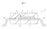
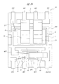
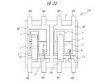
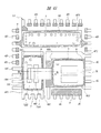
図1〜図5は、本実施の形態の半導体装置を示す図であり、図1は外観を示す平面図、図2は外観を示す側面図、図3は内部構造を示す平面図、図4は図3のA−A線に沿った断面図、図5は図3のB−B線に沿った断面図である。
(Embodiment 1)
1 to 5 are diagrams showing a semiconductor device according to the present embodiment. FIG. 1 is a plan view showing an appearance, FIG. 2 is a side view showing the appearance, FIG. 3 is a plan view showing an internal structure, and FIG. Is a cross-sectional view taken along line AA in FIG. 3, and FIG. 5 is a cross-sectional view taken along line BB in FIG.
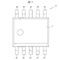
本実施の形態の半導体装置1Aは、シリコンチップ3をエポキシ系のモールド樹脂2で封止した面実装型パッケージであり、モールド樹脂2の2つの側面には、半導体装置1Aの外部接続端子を構成するリード4のアウターリード部が5本ずつ露出している。これら10本のリード4のうち、図1に示すモールド樹脂2の上辺に沿って配置された5本のリード4は、ドレインリード4Dである。また、モールド樹脂2の下辺に沿って配置された5本のリード4のうち、中央の1本はゲートリード4Gであり、残り4本はソースリード4Sである。
The semiconductor device 1A of the present embodiment is a surface-mount package in which a
上記シリコンチップ3の平面寸法は、例えば長辺×短辺=3.9mm×2.2mmである。シリコンチップ3の主面には、携帯情報機器の電力制御スイッチや充放電保護回路スイッチなどに使用されるパワーMOSFET(後述)が形成されている。
The planar dimension of the
また、上記シリコンチップ3は、5本のドレインリード4Dと一体に形成されたダイパッド部4Pの上に、その主面を上に向けた状態で搭載されている。シリコンチップ3の裏面は、パワーMOSFETのドレインを構成しており、Agペースト5を介してダイパッド部4Pの上面に接合されている。ダイパッド部4Pおよび10本のリード4(ドレインリード4D、ゲートリード4G、ソースリード4S)は、CuまたはFe−Ni合金からなり、それらの表面には、Pd膜を主成分とし、その上下にNi膜とAu膜とを積層した3層構造(Ni/Pd/Au)のメッキ層(図示せず)が形成されている。Agペースト5の組成およびメッキ層の効果については、後述する。
The
図3に示すように、シリコンチップ3の主面には、ソースパッド7およびゲートパッド8が形成されている。後述するように、ソースパッド7およびゲートパッド8のそれぞれは、シリコンチップ3の最上層に形成されたAl膜を主体とする導電膜によって構成されている。ソースパッド7は、パワーMOSFETのオン抵抗を低減するために、ゲートパッド8よりも広い面積を有している。同様の理由から、シリコンチップ3の裏面は、その全面がパワーMOSFETのドレインを構成している。
As shown in FIG. 3, a
本実施の形態の半導体装置1Aは、シリコンチップ3の主面に2個のソースパッド7と1個のゲートパッド8を形成し、2個のソースパッド7の間にゲートパッド8を配置している。
In the semiconductor device 1A of the present embodiment, two
図6(a)は、パワーMOSFETを含むパッケージの模式的回路図である。図のように、パワーMOSFETは複数のMOSFETが並列に接続されて構成されていると近似できる。図中のR1〜Rnは、ソースパッド7から各パワーMOSFETのソース領域までの抵抗を表している。例えばR1は、ソースパッド7から最も近い位置にあるソース領域までの抵抗を表し、Rnは、ソースパッド7から最も遠い位置にあるソース領域までの抵抗を表している。
FIG. 6A is a schematic circuit diagram of a package including a power MOSFET. As shown in the figure, the power MOSFET can be approximated by a configuration in which a plurality of MOSFETs are connected in parallel. R1 to Rn in the figure represent resistances from the
図6(b)は、シリコンチップ3の主面の中心に対してソースパッド7とゲートパッド8を非対称に配置した比較例のパッケージを示す平面図、図6(c)は、ソースパッド7の間にゲートパッド8を配置した本実施の形態のパッケージを示す平面図である。図6(b)に示す比較例の場合は、ソースパッド7から最も遠いソース領域の位置(X)までの距離(D1)が大きいため、R1に対してRnが非常に大きくなり、パッケージ全体のソース抵抗が大きくなる。これに対し、図6(c)に示す本実施の形態では、ソースパッド7から最も遠いソース領域の位置(Y)までの距離(D2)を小さくできるため、R1に対するRnの増分は、比較例よりも小さくなる。このように、2個のソースパッド7の間にゲートパッド8を配置する本実施の形態によれば、図6(b)に示す比較例に比べてパッケージ全体のソース抵抗を小さくすることができる。
6B is a plan view showing a package of a comparative example in which the
図3に示すように、本実施の形態の半導体装置1Aは、ゲートリード4Gの右側に配置された2本のソースリード4Sおよびゲートリード4Gの左側に配置された2本のソースリード4Sがそれぞれモールド樹脂2の内部で互いに連結されており、この連結された部分とソースパッド7とがそれぞれ1本のAlリボン10を介して電気的に接続されている。Alリボン10の厚さは0.1mm程度であり、幅は1mm程度である。パワーMOSFETのオン抵抗を低減するためには、Alリボン10の幅をソースパッド7の幅に近づけることによって、Alリボン10とソースパッド7の接触面積をできるだけ大きくすることが望ましい。一方、ソースリード4Sより面積の小さいゲートパッド8は、1本のAuワイヤ11を介してゲートリード4Gと電気的に接続されている。
As shown in FIG. 3, the semiconductor device 1A of the present embodiment includes two source leads 4S arranged on the right side of the
次に、上記シリコンチップ3に形成されたパワーMOSFETについて説明する。図7は、パワーMOSFETの一例であるnチャネル型のトレンチゲート型パワーMOSFETを示すシリコンチップ3の要部断面図である。
Next, the power MOSFET formed on the
n+型単結晶シリコン基板20の主面には、n−型単結晶シリコン層21がエピタキシャル成長法によって形成されている。n+型単結晶シリコン基板20およびn−型単結晶シリコン層21は、パワーMOSFETのドレインを構成している。
An n − type single
n−型単結晶シリコン層21の一部には、p型ウエル22が形成されている。また、n−型単結晶シリコン層21の表面の一部には、酸化シリコン膜23が形成されており、他の一部には複数の溝24が形成されている。n−型単結晶シリコン層21の表面のうち、酸化シリコン膜23で覆われた領域は、素子分離領域を構成し、溝24が形成された領域は、素子形成領域(アクティブ領域)を構成している。図示はしないが、溝24の平面形状は、四角形、六角形、八角形などの多角形または一方向に延在するストライプである。
A p-
溝24の底部および側壁には、パワーMOSFETのゲート酸化膜を構成する酸化シリコン膜25が形成されている。また、溝24の内部には、パワーMOSFETの下層ゲート電極を構成する多結晶シリコン膜26Aが埋め込まれている。一方、酸化シリコン膜23の上部には、上記下層ゲート電極を構成する多結晶シリコン膜26Aと同一工程で堆積した多結晶シリコン膜からなるゲート引き出し電極26Bが形成されている。下層ゲート電極(多結晶シリコン膜26A)とゲート引き出し電極26Bは、図示しない領域で電気的に接続されている。
A
素子形成領域のn−型単結晶シリコン層21には、溝24よりも浅いp−型半導体領域27が形成されている。このp−型半導体領域27は、パワーMOSFETのチャネル層を構成している。p−型半導体領域27の上部には、p−型半導体領域27より不純物濃度の高いp型半導体領域28が形成されており、さらにp型半導体領域28の上部には、n+型半導体領域29が形成されている。p型半導体領域28は、パワーMOSFETのパンチスルーストッパー層を構成し、n+型半導体領域29は、ソースを構成している。
A p −
上記パワーMOSFETが形成された素子形成領域の上部、およびゲート引き出し電極26Bが形成された素子分離領域の上部には、2層の酸化シリコン膜30、31が形成されている。素子形成領域には、酸化シリコン膜31、30、p型半導体領域28およびn+型半導体領域29を貫通してp−型半導体領域27に達する接続孔32が形成されている。また、素子分離領域には、酸化シリコン膜31、30を貫通してゲート引き出し電極26Bに達する接続孔33が形成されている。
Two layers of
接続孔32、33の内部を含む酸化シリコン膜31の上部には、薄いTiW(チタンタングステン)膜と厚いAl膜との積層膜で構成されたソース電極40およびゲート電極41が形成されている。素子形成領域に形成されたソース電極40は、接続孔32を通じてパワーMOSFETのソース(n+型半導体領域29)に電気的に接続されている。この接続孔32の底部には、ソースパッド7とp−型半導体領域27とをオーミック接触させるためのp+型半導体領域35が形成されている。また、素子分離領域に形成されたゲート電極41は、接続孔33の下部のゲート引き出し電極26Bを介してパワーMOSFETの下層ゲート電極(多結晶シリコン膜26A)に接続されている。
A
ソース電極40およびゲート電極41の上部には、酸化シリコン膜と窒化シリコン膜との積層膜で構成された表面保護膜42が形成されている。そして、表面保護膜42の一部を除去してソース電極40を露出することによってソースパッド7が形成され、表面保護膜42の他の一部を除去してゲート電極41を露出することによってゲートパッド8が形成されている。
On the
上述したように、ソースパッド7にはAlリボン10の一端がウェッジボンディング法によって電気的に接続されている。ソースパッド7は、Alリボン10をボンディングする際にパワーMOSFETが受ける衝撃を緩和するため、酸化シリコン膜30、31の上部における厚さを3μm以上とすることが望ましい。
As described above, one end of the
図8は、シリコンチップ3に形成されたソース電極40およびゲート電極41を含む最上層の導電膜を示す平面図である。シリコンチップ3の外周部には、Al配線36、37、38が形成されている。Al配線36、37、38は、ソース電極40およびゲート電極41と同層の導電膜(TiW膜とAl膜との積層膜)で構成されている。実際のシリコンチップ3は、ソース電極40、ゲート電極41およびAl配線36、37、38が表面保護膜42によって覆われているので、シリコンチップ3の表面には、上記した最上層の導電膜のうち、ソースパッド7が形成された領域のソース電極40と、ゲートパッド8が形成された領域のゲート電極41のみが露出している。
FIG. 8 is a plan view showing the uppermost conductive film including the
図9は、本実施の形態の半導体装置1Aの製造工程の一例を示すフロー図である。半導体装置1Aを製造するには、まず、通常の製造方法に従ってシリコンウエハにパワーMOSFETを形成した後、このシリコンウエハをダイシングしてシリコンチップ3を得る。次に、リード4およびダイパッド部4Pが形成されたリードフレームを用意し、Agペースト5を使ってダイパッド部4P上にシリコンチップ3をダイボンディングする。
FIG. 9 is a flowchart showing an example of the manufacturing process of the semiconductor device 1A of the present embodiment. To manufacture the semiconductor device 1A, first, a power MOSFET is formed on a silicon wafer according to a normal manufacturing method, and then the
次に、超音波を利用したウェッジボンディング法を用いて、シリコンチップ3のソースパッド7とソースリード4SとをAlリボン10で電気的に接続する。続いて、熱と超音波を利用したボールボンディング法を用いて、シリコンチップ3のゲートパッド8とゲートリード4GとをAuワイヤ11で電気的に接続する。
Next, the
次に、モールド金型を用いてシリコンチップ3(およびダイパッド部4P、Alリボン10、Auワイヤ11、リード4のインナーリード部)をモールド樹脂2で封止した後、モールド樹脂2の表面に製品名や製造番号などをマーキングする。続いて、モールド樹脂2の外部に露出したリード4の不要部分を切断・除去した後、リード4をガルウィング状に成形し、最後に、製品の良・不良を判別する選別工程を経て半導体装置1Aが完成する。
Next, the silicon chip 3 (and the
このように、本実施の形態では、ゲートパッド8よりも広い面積を有するソースパッド7とソースリード4Sとを電気的に接続する導電材料として、Auワイヤ11よりも広い面積を有するAlリボン10を使用する。そのため、ソースパッド7の表面にAlリボン10をウェッジボンディングする際には、図10に示すように、シリコンチップ3の表面だけでなく、シリコンチップ3とダイパッド部4Pとの間に介在するAgペースト5にもボンディングツール12の大きな振動エネルギーが加わる。従って、ボンディングツールの大きな振動エネルギーによってAgペースト5にクラックが発生するのを防ぐ対策として、最適な弾性率(Pa)を持ったAgペースト5を選択的に使用することが望ましい。
Thus, in the present embodiment, the
本実施の形態では、Agペースト5の弾性率(Pa)を、以下の式(1)で定義する。
弾性率(Pa)=2.6×接着厚さ(μm)/破断変位(μm)×剪断強度(Pa) (1)
式(1)において、接着厚さはAgペーストの厚さ(μm)、剪断強度(Pa)は剪断方向の力/断面積(接着面積)である。また、破断変位は、図11に示す計算式から導出される値(μm)である。ここで、破断変位>Alリボン超音波ボンディング可能変位(=Alリボンの超音波ボンディング時にボンディングツールを振動させることによって、Agペーストが変形する量)となるので、本実施の形態のAgペースト5に要求される弾性率(Pa)の選択指針式は、{弾性率(Pa)<2.6×接着厚さ(μm)/Alリボン超音波ボンディング可能変位(μm)×剪断強度(Pa)}となる。
In the present embodiment, the elastic modulus (Pa) of the
Elastic modulus (Pa) = 2.6 × bonding thickness (μm) / breaking displacement (μm) × shear strength (Pa) (1)
In formula (1), the adhesion thickness is the thickness (μm) of the Ag paste, and the shear strength (Pa) is the force / cross-sectional area (adhesion area) in the shear direction. Further, the breaking displacement is a value (μm) derived from the calculation formula shown in FIG. Here, fracture displacement> Al ribbon ultrasonic bonding possible displacement (= Amount of Ag paste deformed by vibrating bonding tool during ultrasonic bonding of Al ribbon). The required guideline formula for elastic modulus (Pa) is {elastic modulus (Pa) <2.6 × bonding thickness (μm) / Al ribbon ultrasonic bondable displacement (μm) × shear strength (Pa)}. Become.
次に、上記した選択指針式の有効性を確認するために行ったクラック耐性実験について説明する。この実験で使用した市販の4種類のAgペースト(1〜4)の弾性率、剪断強度、接着厚さを表1に示す。Alリボンの超音波ボンディング時におけるAgペーストの変位量は、Agペースト(1)、(3)、(4)がそれぞれ0.1218μmであり、Agペースト(2)が0.07μmである。 Next, a crack resistance experiment conducted to confirm the effectiveness of the above-described selection guide type will be described. Table 1 shows the elastic modulus, shear strength, and adhesion thickness of four types of commercially available Ag pastes (1 to 4) used in this experiment. The amount of displacement of the Ag paste during ultrasonic bonding of the Al ribbon is 0.1218 μm for Ag pastes (1), (3), and (4), and 0.07 μm for Ag paste (2).

図12は、4種類のAgペースト(1〜4)の選択指針式と実験結果を示すグラフである。各グラフの実線は、式(1)から算出される各Agペースト(1〜4)の弾性率を示しており、実線よりも下側の領域は、選択指針式を満たす領域、すなわちボンディング可能領域を表している。また、各グラフの黒点は、各Agペースト(1〜4)の実際の弾性率を示している。 FIG. 12 is a graph showing selection guideline formulas and experimental results for four types of Ag pastes (1 to 4). The solid line in each graph indicates the elastic modulus of each Ag paste (1 to 4) calculated from the formula (1), and the area below the solid line is the area that satisfies the selection guideline formula, that is, the bondable area. Represents. Moreover, the black point of each graph has shown the actual elasticity modulus of each Ag paste (1-4).
実験結果によれば、実際の弾性率が選択指針式を満たしていたAgペースト(3および4)ではクラックが発生しなかったが、選択指針式を満たしていないAgペースト(1および2)ではクラックが発生した。この実験結果から、ダイパッド部4P上にシリコンチップ3を接合する際、上記選択指針式を満たすAgペースト5を選択することによって、ボンディングツールの振動エネルギーによるAgペースト5のクラックを有効に回避できることが確認された。
According to the experimental results, cracks did not occur in the Ag pastes (3 and 4) whose actual elastic modulus satisfied the selection guideline formula, but cracks did not occur in the Ag pastes (1 and 2) that did not satisfy the selection guideline formula. There has occurred. From this experimental result, when bonding the
図13は、Agペーストの厚さを10μmに設定し、標準的な超音波ボンディング出力(4W)でAlリボンをボンディングした場合におけるAgペーストの弾性率の剪断強度依存性を測定した結果を示すグラフである。グラフ中の白丸はクラックが発生しなかった例であり、黒丸はクラックが発生した例である。 FIG. 13 is a graph showing the results of measuring the shear strength dependence of the elastic modulus of the Ag paste when the thickness of the Ag paste is set to 10 μm and the Al ribbon is bonded with a standard ultrasonic bonding output (4 W). It is. White circles in the graph are examples in which no cracks occurred, and black circles are examples in which cracks occurred.
この測定結果から、Agペーストの弾性率は0.2〜5.3GPaの範囲が望ましく、剪断強度(MPa)は8.5MPa以上が望ましいと判断される。弾性率が0.2GPa未満では、Agの含有量が少なすぎて所望の電気伝導率が得られない。他方、5.3GPaよりも大きい場合は、Agペーストの硬度が高すぎて変形できないため、超音波ボンディング時の振動に追従できなくなってクラックが発生する。また、Agペーストの剪断強度が8.5MPa未満の場合は、超音波ボンディング時に生じる衝撃に耐えられなくなる。 From this measurement result, it is determined that the elastic modulus of the Ag paste is desirably in the range of 0.2 to 5.3 GPa, and the shear strength (MPa) is desirably 8.5 MPa or more. If the elastic modulus is less than 0.2 GPa, the desired electrical conductivity cannot be obtained because the Ag content is too small. On the other hand, if it is higher than 5.3 GPa, the hardness of the Ag paste is too high to deform, and it becomes impossible to follow the vibration during ultrasonic bonding and cracks occur. Further, when the shear strength of the Ag paste is less than 8.5 MPa, it cannot withstand the impact generated during ultrasonic bonding.
次に、リードフレーム(ダイパッド部4Pおよびリード4)の表面にPd膜を主成分とするメッキ層を形成した効果について説明する。表2は、Cuからなるリードフレームの表面に3種類(Ag、Ni、Pd)のメッキ単層を形成した場合と、メッキ層を形成しない場合(Cuベア)とにおいて、ソースリードとAlリボン、ゲートリードとAuワイヤ、ダイパッド部とAgペーストのそれぞれの接着性を示したものである(○印は良好な接着性を示し、×印は接着不良を示す)。
Next, the effect of forming a plating layer mainly composed of a Pd film on the surface of the lead frame (die
表2から明らかなように、リードフレームの表面にPd膜を主成分とするメッキ層を形成した場合は、ソースリード(ソースポスト)とAlリボン、ゲートリード(ゲートポスト)とAuワイヤ、ダイパッド部とAgペーストのすべてが良好な接着性を示すことが分かる。 As is apparent from Table 2, when a plating layer mainly composed of a Pd film is formed on the surface of the lead frame, the source lead (source post) and Al ribbon, the gate lead (gate post) and Au wire, and the die pad portion It can be seen that all of the Ag paste and the Ag paste exhibit good adhesion.
また、表3から明らかなように、リードフレームの表面にPd膜を主成分とするメッキ層を形成した場合は、ゲートパッドとゲートリードをAlワイヤで接続する場合でも良好な接着性を示す。このように、リードフレームの表面にPd膜を主成分とするメッキ層を形成することにより、一種類のメッキ材料ですべての接続に対応することが可能となるので、製造工程を簡略化することができる。 Further, as is apparent from Table 3, when a plating layer mainly composed of a Pd film is formed on the surface of the lead frame, good adhesion is exhibited even when the gate pad and the gate lead are connected by an Al wire. In this way, by forming a plating layer mainly composed of a Pd film on the surface of the lead frame, it becomes possible to handle all connections with a single type of plating material, thus simplifying the manufacturing process. Can do.
このように、本実施の形態によれば、ソースリード4Sとソースパッド7をAlリボン10で接続することにより、両者をAuワイヤで接続する場合に比べてボンディング面積が大きくなるので半導体装置1Aの低抵抗化を実現することができる。また、Alリボン10はAuワイヤよりも原価が低廉であることから、半導体装置1Aの製造コストを低減することができる。なお、要求される抵抗値が同一であれば、ソースリード4Sとソースパッド7をAuワイヤで接続する場合に比べて、ソースパッド7ひいてはシリコンチップ3のサイズを縮小することができるので、この場合も、半導体装置1Aの製造コストを低減することができる。
As described above, according to the present embodiment, since the source lead 4S and the
また、本実施の形態によれば、Agペースト5の弾性率および剪断強度を最適化することによって、Alリボン10の超音波ボンディングに起因するAgペースト5のクラックを防止することができるので、半導体装置1Aの製造歩留まりおよび信頼性が向上する。
In addition, according to the present embodiment, by optimizing the elastic modulus and shear strength of the
また、本実施の形態によれば、リードフレーム(ダイパッド部4Pおよびリード4)の表面にPd膜を主成分とするメッキ層を形成することにより、半導体装置1AのPbフリー化を実現することができる。
In addition, according to the present embodiment, it is possible to realize the Pb-free semiconductor device 1A by forming the plating layer mainly composed of a Pd film on the surface of the lead frame (die
(実施の形態2)
図14は、本実施の形態の半導体装置の内部構造を示す平面図である。本実施の形態の半導体装置1Bと前記実施の形態1の半導体装置1Aは、外部接続端子(リード4)の数およびそれらの配置が異なっている。
(Embodiment 2)
FIG. 14 is a plan view showing the internal structure of the semiconductor device of the present embodiment. The semiconductor device 1B of the present embodiment and the semiconductor device 1A of the first embodiment are different in the number of external connection terminals (leads 4) and their arrangement.
すなわち、本実施の形態の半導体装置1Bは、モールド樹脂2の2つの側面にリード4のアウターリード部が4本ずつ露出している。これら8本のリード4のうち、図14に示すパッケージの上辺に沿って配置された4本のリード4は、3本のドレインリード4Dと1本のゲートリード4Gである。また、パッケージの下辺に沿って配置された4本のリード4は、ソースリード4Sである。そして、シリコンチップ3は、3本のドレインリード4Dと一体に形成されたダイパッド部4Pの上に搭載されている。図には示さないが、シリコンチップ3の裏面は、パワーMOSFETのドレインを構成しており、前記実施の形態1で用いたものと同一のAgペースト5を介してダイパッド部4Pの上面に接合されている。
That is, in the
上記シリコンチップ3の主面には、ソースパッド7およびゲートパッド8が形成されている。上述したように、本実施の形態の半導体装置1Bは、ドレインリード4Dとゲートリード4Gをモールド樹脂2の同一側面に配置している。このため、ゲートパッド8は、ゲートリード4Gの近傍のコーナー部に配置され、Auワイヤ11を介してゲートリード4Gと電気的に接続されている。
A
一方、図14に示すパッケージの下辺に沿って配置された4本のソースリード4Sは、モールド樹脂2の内部で互いに連結されており、この連結された部分とソースパッド7とがAlリボン10を介して電気的に接続されている。
On the other hand, the four source leads 4S arranged along the lower side of the package shown in FIG. 14 are connected to each other inside the
本実施の形態では、ゲートパッド8をシリコンチップ3の主面のコーナー部に配置したことにより、シリコンチップ3の主面に形成されたソースパッド7の面積が前記実施の形態1のそれよりも大きくなっている。このため、ソースリード4Sとソースパッド7は、3本のAlリボン10を介して接続されている。
In the present embodiment, the
また、上記3本のAlリボン10のうち、真ん中のAlリボン10は、シリコンチップ3の主面の中央に配置されており、残り2本のAlリボン10は、真ん中のAlリボン10から等しい距離だけ離れて配置されている。3本のAlリボン10をこのように配置することにより、前記実施の形態1と同様の効果が得られるので、パワーMOSFETのオン抵抗が低減される。
Of the three
また、本実施の形態によれば、前記実施の形態1に比べてソースパッド7の面積が増加したことにより、ソースパッド7に接続されるAlリボン10の数を増やすことができる。これにより、ソースパッド7とAlリボン10の接触面積が増加し、その分、パワーMOSFETのオン抵抗が小さくなるので、デバイス性能が向上した半導体装置1Bを実現することができる。
Further, according to the present embodiment, the number of
(実施の形態3)
図15は、本実施の形態の半導体装置の内部構造を示す平面図である。本実施の形態の半導体装置1Cと前記実施の形態1の半導体装置1Aは、外部接続端子(リード4)の数およびそれらの配置が異なっている。
(Embodiment 3)
FIG. 15 is a plan view showing the internal structure of the semiconductor device of the present embodiment. The number of external connection terminals (leads 4) and their arrangement differ between the semiconductor device 1C of the present embodiment and the semiconductor device 1A of the first embodiment.
本実施の形態の半導体装置1Cは、モールド樹脂2の2つの側面にリード4のアウターリード部が4本ずつ露出している。これら8本のリード4のうち、図15に示すパッケージの上辺に沿って配置された4本のリード4は、ドレインリード4Dである。また、パッケージの下辺に沿って配置された4本のリード4は、3本のソースリード4Sと1本のゲートリード4Gである。すなわち、本実施の形態の半導体装置1Cは、外部接続端子の配置が既存のSOP8と同一になっている。
In the
シリコンチップ3は、4本のドレインリード4Dと一体に形成されたダイパッド部4Pの上に搭載されている。図には示さないが、シリコンチップ3の裏面は、パワーMOSFETのドレインを構成しており、前記実施の形態1で用いたものと同一のAgペースト5を介してダイパッド部4Pの上面に接合されている。
The
上記シリコンチップ3の主面には、ソースパッド7およびゲートパッド8が形成されている。ゲートパッド8は、ゲートリード4Gの近傍のコーナー部に配置され、Auワイヤ11を介してゲートリード4Gと電気的に接続されている。一方、図15に示すパッケージの下辺に沿って配置された3本のソースリード4Sは、モールド樹脂2の内部で互いに連結されており、この連結された部分とソースパッド7とが2本のAlリボン10を介して電気的に接続されている。
A
上記2本のAlリボン10は、ソースパッド7の中心から等しい距離だけ離れて配置されている。2本のAlリボン10をこのように配置することにより、前記実施の形態1と同様の効果が得られるので、パワーMOSFETのオン抵抗が低減される。すなわち、本実施の形態によれば、外部接続端子の配置を既存のSOP8と同一にしたままで、デバイス性能を向上させることができる。
The two
(実施の形態4)
図16〜図19は、本実施の形態の半導体装置を示す図であり、図16は内部構造を示す平面図、図17は裏面側の外観を示す平面図、図18は図16のC−C線に沿った断面図、図19は内部等価回路図である。
(Embodiment 4)
16 to 19 are views showing the semiconductor device of the present embodiment, in which FIG. 16 is a plan view showing the internal structure, FIG. 17 is a plan view showing the appearance of the back side, and FIG. FIG. 19 is a sectional view taken along line C, and FIG. 19 is an internal equivalent circuit diagram.
本実施の形態の半導体装置1Dは、2個のシリコンチップ3H、3Lをモールド樹脂2で封止した面実装型パッケージであり、モールド樹脂2の2つの側面には、外部接続端子を構成するリード4のアウターリード部が4本ずつ露出している。
The semiconductor device 1D according to the present embodiment is a surface-mount package in which two
上記2個のシリコンチップ3H、3Lのうち、面積の小さいシリコンチップ3Hの主面には、ハイサイドMOSFETが形成されており、面積の大きいシリコンチップ3Lの主面には、ロウサイドMOSFETが形成されている。図19に示すように、ハイサイドMOSFETのソースとロウサイドMOSFETのドレインとは電気的に接続され、これによって、例えばDC−DCコンバータが構成されている。ハイサイドMOSFETおよびロウサイドMOSFETの具体的な構造は、前記実施の形態1のパワーMOSFETとほぼ同一であるため、それらの図示は省略する。
Of the two
また、上記2個のシリコンチップ3H、3Lのうち、面積の小さいシリコンチップ3Hは、2本のドレインリード4D1と一体に形成されたダイパッド部4P1の上に、その主面を上に向けた状態で搭載されている。シリコンチップ3Hの裏面は、ハイサイドMOSFETのドレインを構成しており、実施の形態1で用いたものと同一のAgペースト5を介してダイパッド部4P1の上面に接合されている。
Of the two
図16に示すモールド樹脂2の下辺には、上記2本のドレインリード4D1を挟んでそれらの両側にゲートリード4G1とソースリード4S1が1本ずつ配置されている。また、シリコンチップ3Hの主面には、大面積のソースパッド7と小面積のゲートパッド8が形成されている。そして、シリコンチップ3Hのソースパッド7とソースリード4S1とが1本のAuワイヤ11を介して電気的に接続され、シリコンチップ3Hのゲートパッド8とゲートリード4G1とが1本のAuワイヤ11を介して電気的に接続されている。
On the lower side of the
一方、面積の大きいシリコンチップ3Lは、上記ダイパッド部4P1よりも面積の大きいダイパッド部4P2の上に、その主面を上に向けた状態で搭載されている。このシリコンチップ3Lの主面には、大面積のソースパッド7と小面積のゲートパッド8とが形成されている。また、シリコンチップ3Lの裏面は、ロウサイドMOSFETのドレインを構成しており、実施の形態1で用いたものと同一のAgペースト5を介してダイパッド部4P2の上面に接合されている。
On the other hand, the
図16に示すモールド樹脂2の上辺には、3本のソースリード4S2と1本のゲートリード4G2が配置されている。3本のソースリード4S2は、モールド樹脂2の内部で互いに連結されており、この連結された部分とシリコンチップ3Lのソースパッド7とが2本のAlリボン10を介して電気的に接続されている。また、シリコンチップ3Lのゲートパッド8は、1本のAuワイヤ11を介してゲートリード4G2と電気的に接続されている。
On the upper side of the
また、図16に示すように、シリコンチップ3Hが搭載されたダイパッド部4P1の近傍には、シリコンチップ3Lが搭載されたダイパッド部4P2と一体に形成された2本のドレインリード4D2が配置されている。そして、これらのドレインリード4D2とシリコンチップ3Hのソースパッド7がAuワイヤ11を介して電気的に接続されており、これによって、ハイサイドMOSFETのソースとロウサイドMOSFETのドレインとが電気的に接続されている(図19参照)。
Also, as shown in FIG. 16, two drain leads 4D2 formed integrally with the die pad portion 4P2 on which the
また、図17に示すように、モールド樹脂2の裏面には、上記2つのダイパッド部4P1、4P2の裏面が露出している。これにより、半導体装置1Dを配線基板などに実装する際に、ダイパッド部4P1、4P2の裏面を配線基板上の配線に半田付けすることができるので、2個のシリコンチップ3H、3Lで発生した熱を効率的に外部に逃がすことができ、パッケージの熱抵抗を下げることができる。
Further, as shown in FIG. 17, the back surfaces of the two die pad portions 4P1 and 4P2 are exposed on the back surface of the
このように、本実施の形態の半導体装置1Dは、モールド樹脂2で封止された2個のシリコンチップ3H、3Lのうち、面積の大きいシリコンチップ3Lのソースパッド7とソースリード4S2をAlリボン10で接続する。これにより、ソースパッド7とソースリード4S2をAuワイヤで接続する場合に比べて、ロウサイドMOSFETのオン抵抗を低減することができる。なお、シリコンチップ3Lのソースパッド7とソースリード4S2を2本のAlリボン10で接続する場合は、2本のAlリボン10をシリコンチップ3Lの中心から等しい距離だけ離して配置することが望ましい。これにより、ロウサイドMOSFETのオン抵抗をより低減することが可能となる。
As described above, in the semiconductor device 1D of the present embodiment, of the two
ハイサイドMOSFETのソースとロウサイドMOSFETのドレインを電気的に接続する場合は、図20に示すように、ダイパッド部4P1上に搭載されたシリコンチップ3Hのソースパッド7と、シリコンチップ3Lが搭載されたダイパッド部4P2とをAuワイヤ11で直接接続してもよい。
When the source of the high-side MOSFET and the drain of the low-side MOSFET are electrically connected, as shown in FIG. 20, the
ただし、この場合は、シリコンチップ3LとAuワイヤ11とが接近するので、ボンディング条件によっては、シリコンチップ3Lとダイパッド部4P2との隙間から外側に滲み出した導電性のAgペースト5にAuワイヤ11が接触し、Auワイヤ11の接続信頼性が低下する恐れがある。このような不具合を確実に避けるためには、ダイパッド部4P2上に搭載するシリコンチップ3Lのサイズを小さくしなければならないが、その場合は、シリコンチップ3Lのソースパッド7とAlリボン10との接触面積も小さくなるので、ロウサイドMOSFETのオン抵抗を低減することが困難となる。
However, in this case, since the
従って、ハイサイドMOSFETのソースとロウサイドMOSFETのドレインを電気的に接続する場合は、図16に示したように、ダイパッド部4P1の近傍にダイパッド部4P2と一体に形成されたドレインリード4D2を配置し、このドレインリード4D2とシリコンチップ3Hのソースパッド7をAuワイヤ11で接続することが望ましい。
Therefore, when electrically connecting the source of the high-side MOSFET and the drain of the low-side MOSFET, as shown in FIG. 16, the drain lead 4D2 formed integrally with the die pad portion 4P2 is disposed in the vicinity of the die pad portion 4P1. It is desirable to connect the drain lead 4D2 and the
また、本実施の形態では、図18に示すように、ドレインリード4D2に曲げ加工を施すことによって、その高さをダイパッド部4P2よりも高くする。このようにした場合は、図21に示すように、シリコンチップ3Lとダイパッド部4P2との隙間から多量のAgペースト5が外側に滲み出した場合でも、このAgペースト5がドレインリード4D2のボンディング領域まで達することがないので、Agペースト5とAuワイヤ11の干渉を確実に防止することができる。
In the present embodiment, as shown in FIG. 18, the drain lead 4D2 is bent so that its height is higher than that of the die pad portion 4P2. In this case, as shown in FIG. 21, even when a large amount of
また、このようにした場合は、図17に示したように、モールド樹脂2の裏面にダイパッド部4P1を露出させても、ドレインリード4D2が露出することはない。従って、ダイパッド部4P1、4P2の裏面を配線基板上に半田付けする際、ダイパッド部4P1とその近傍のドレインリード4D2とが半田を介して短絡する不良の発生を確実に防止することができる。
In this case, as shown in FIG. 17, even if the die pad portion 4P1 is exposed on the back surface of the
本実施の形態の半導体装置1Dは、上記した構成に限定されるものではなく、例えば図22および図23(図22のD−D線に沿った断面図)に示すように、ドレインリード4D2およびソースリード4S1を一体化して1本のリード(4S1/D2)とし、このリード(4S1/D2)とシリコンチップ3Hのソースパッド7をAuワイヤ11で接続することによって、ハイサイドMOSFETのソースとロウサイドMOSFETのドレインを電気的に接続することもできる。
The semiconductor device 1D of the present embodiment is not limited to the configuration described above. For example, as shown in FIGS. 22 and 23 (cross-sectional view taken along the line DD in FIG. 22), the drain leads 4D2 and The source lead 4S1 is integrated to form one lead (4S1 / D2), and the lead (4S1 / D2) and the
この場合においても、Agペースト5とAuワイヤ11との干渉や、半田によるリード(4S1/D2)とダイパッド部4P1との短絡を防止するためには、図23に示すように、モールド樹脂2の内部において、リード(4S1/D2)の高さをダイパッド部4P2よりも高くすることが望ましい。
Even in this case, in order to prevent the interference between the
(実施の形態5)
例えばシリコンチップ3Lのサイズが比較的小さい場合や、シリコンチップ3Hのサイズが比較的大きい場合などには、図24や図25に示すように、シリコンチップ3Hのソースパッド7とダイパッド部4P2をAlリボン10で直接接続してもよい。この場合は、シリコンチップ3Lに形成されたロウサイドMOSFETのオン抵抗だけでなく、シリコンチップ3Hに形成されたハイサイドMOSFETのオン抵抗も低減することができる。
(Embodiment 5)
For example, when the size of the
また、例えば図26に示すように、ドレインリード4D2とソースリード4S1とを一体化して一本のリード(4S1/D2)にした場合は、リード(4S1/D2)の面積が大きくなるので、シリコンチップ3Hのソースパッド7とリード(4S1/D2)をAlリボン10で接続することによって、ハイサイドMOSFETのオン抵抗を低減することが可能となる。
Further, for example, as shown in FIG. 26, when the drain lead 4D2 and the source lead 4S1 are integrated into a single lead (4S1 / D2), the area of the lead (4S1 / D2) becomes large. By connecting the
(実施の形態6)
図27に示すように、本実施の形態の半導体装置1Eは、ダイパッド部4P2上にシリコンチップ3Lを搭載する際、シリコンチップ3Lの長辺を8本のリード4の延在方向と平行に配置してもよい。この場合は、シリコンチップ3Lのソースパッド7とソースリード4S2を接続するAlリボン10の延在方向がシリコンチップ3Lの長辺と平行になるので、ソースパッド7に接続されるAlリボン10が1本であっても、ソースパッド7とAlリボン10の接触面積を増やしてロウサイドMOSFETのオン抵抗を低減することが可能となる。
(Embodiment 6)
As shown in FIG. 27, in the semiconductor device 1E of the present embodiment, when the
(実施の形態7)
図28に示す半導体装置1Fは、ドレインリード4Dと一体に形成されたダイパッド部4P上に2個のシリコンチップ3を搭載した例であり、図29はこの半導体装置1Fの内部等価回路図である。
(Embodiment 7)
A semiconductor device 1F shown in FIG. 28 is an example in which two
2個のシリコンチップ3の裏面は、パワーMOSFETのドレインを構成しており、前記実施の形態1で用いたものと同一のAgペースト5を介してダイパッド部4Pの上面に接合されている。また、2個のシリコンチップ3の主面には、ソースパッド7およびゲートパッド8が形成されている。そして、ソースパッド7とソースリード4SがAlリボン10を介して電気的に接続され、ゲートパッド8とゲートリード4GがAuワイヤ11を介して電気的に接続されている。
The back surfaces of the two
この場合も、2個のシリコンチップ3のソースパッド7とソースリード4SをAlリボン10で接続することにより、それぞれのシリコンチップ3に形成されたパワーMOSFETのオン抵抗を低減することができる。
Also in this case, by connecting the
(実施の形態8)
図30に示す半導体装置1Gは、ダイパッド部4P1の上に搭載されたシリコンチップ3Hのソースパッド7とソースリード4S1、ダイパッド部4P2の上に搭載されたシリコンチップ3Lのソースパッド7とソースリード4S2、シリコンチップ3Hのソースパッド7とダイパッド部4P2をそれぞれAlリボン10で電気的に接続した例であり、図31はこの半導体装置1Gの内部等価回路図である。
(Embodiment 8)
A semiconductor device 1G shown in FIG. 30 includes a
この半導体装置1Gによれば、シリコンチップ3Lに形成されたロウサイドMOSFETのオン抵抗とシリコンチップ3Hに形成されたハイサイドMOSFETのオン抵抗を共に低減することができる。
According to the semiconductor device 1G, it is possible to reduce both the on-resistance of the low-side MOSFET formed on the
(実施の形態9)
図32に示す半導体装置1Hは、ドレインリード4Dと一体に形成された2個のダイパッド部4P上にそれぞれシリコンチップ3を搭載し、それぞれのシリコンチップ3のソースパッド7とソースリード4SをAlリボン10で電気的に接続した例であり、図33はこの半導体装置1Hの内部等価回路図である。
(Embodiment 9)
A
この半導体装置1Hによれば、2個のシリコンチップ3に形成されたパワーMOSFETのオン抵抗を共に低減することができる。
According to this
(実施の形態10)
前記実施の形態1〜9では、1個または2個のシリコンチップをモールド樹脂で封止した面実装型パッケージに適用したが、3個以上のシリコンチップをモールド樹脂で封止した面実装型パッケージに適用することもできる。
(Embodiment 10)
In the first to ninth embodiments, the present invention is applied to a surface mount package in which one or two silicon chips are sealed with a mold resin. However, a surface mount package in which three or more silicon chips are sealed with a mold resin. It can also be applied to.
図34に示す半導体装置1Iは、3個のシリコンチップ3D、3H、3Lをモールド樹脂2で封止したシステム・イン・パッケージ(System In Package:SIP)であり、図35はこの半導体装置1Iの内部等価回路図である。
A semiconductor device 1I shown in FIG. 34 is a system in package (SIP) in which three
3個のシリコンチップ3D、3H、3Lのそれぞれは、前述したAgペースト5を介してダイパッド部4P1、4P2、4P3の上に搭載されている。3個のシリコンチップ3D、3H、3Lのうち、シリコンチップ3Hの主面には、ハイサイドMOSFETが形成されており、シリコンチップ3Lの主面には、ロウサイドMOSFETが形成されている。また、シリコンチップ3Dの主面には、ドライバICまたはコントロールICが形成されている。
Each of the three
この場合も、シリコンチップ3H、3Lのそれぞれのソースパッド7にAlリボン10を接続することにより、シリコンチップ3Lに形成されたロウサイドMOSFETのオン抵抗とシリコンチップ3Hに形成されたハイサイドMOSFETのオン抵抗を共に低減することができるので、システム・イン・パッケージの特性を向上させることができる。
Also in this case, by connecting the
図36に示す半導体装置1Jは、ハイサイドMOSFETが形成された半導体チップ3Hのソースパッド7およびロウサイドMOSFETが形成された半導体チップ3Lのソースパッド7を含めて、3個の半導体チップ3D、3H、3Lの間をAuワイヤ11のみで接続したシステム・イン・パッケージの一例である。
A semiconductor device 1J shown in FIG. 36 includes three
一方、図37に示す半導体装置1Kは、半導体チップ3H、3Lのそれぞれのソースパッド7SH、7SLにAlリボン10H、10Lを接続したシステム・イン・パッケージの一例であり、半導体チップ3Hに形成されたハイサイドMOSFETの素子サイズ、および半導体チップ3Lに形成されたロウサイドMOSFETの素子サイズは、いずれも図36に示す半導体装置1Jのそれと同一である。
On the other hand, the semiconductor device 1K shown in FIG. 37 is an example of a system-in-package in which the
図36と図37とを比較すれば分かるように、ハイサイドMOSFETの素子サイズおよびロウサイドMOSFETの素子サイズがそれぞれ同一であっても、半導体チップ3H、3Lのそれぞれのソースパッド7SH、7SLにAlリボン10H、10Lを接続する場合は、半導体チップ3H、3Lのそれぞれのサイズを小さくすることができる。これは、前述したように、ソースパッド7SH、7SLにAlリボン10H、10Lを接続する場合は、ソースパッド7SH、7SLにAuワイヤ11を接続する場合に比べて接触面積が大きくなり、パワーMOSFETのオン抵抗が小さくなる。また、オン抵抗が同一であれば、ソースパッド7SH、7SLの面積を小さくすることができるので、その分、半導体チップ3H、3Lのサイズを小さくすることができるからである。
As can be seen by comparing FIG. 36 and FIG. 37, even if the element size of the high-side MOSFET and the element size of the low-side MOSFET are the same, the Al ribbon is applied to the source pads 7SH and 7SL of the
半導体チップ3H、3Lのそれぞれのサイズを小さくした場合には、図37に示すように、同一寸法の樹脂パッケージ内に収容する半導体チップ3D搭載用のダイパッド部4P3のサイズを大きくすることができる。従って、ダイパッド部4P3上に搭載する半導体チップ3Dのサイズを大きくすることができ、その分、半導体チップ3Dに形成するパッドの数を増やすことができるので、半導体装置1Jよりも多機能の半導体装置1Kを実現することができる。
When the sizes of the
次に、上記半導体装置1Kの製造工程の一例を図38(全体フロー図)および図39〜図46(工程毎の平面図)を用いて説明する。 Next, an example of the manufacturing process of the semiconductor device 1K will be described with reference to FIG. 38 (overall flow diagram) and FIGS. 39 to 46 (plan view for each process).
まず、通常の製造方法に従ってハイサイドMOSFET、ロウサイドMOSFETおよびドライバIC回路(またはコントロールIC回路)を形成した3種類のシリコンウエハをそれぞれダイシングして半導体チップ3H、3L、3Dを得る。
First, according to a normal manufacturing method, three types of silicon wafers on which a high-side MOSFET, a low-side MOSFET, and a driver IC circuit (or control IC circuit) are formed are diced to obtain
次に、図39に示すように、リード4D、4H、4Lおよびダイパッド部4P1、4P2、4P3が形成されたリードフレームLFを用意する。このリードフレームLFは、Cu合金またはFe−Ni合金からなり、その表面の一部(図中のハッチングを施した領域)には、例えば前記実施の形態1で説明したPd膜を主成分とするメッキ層9が形成されている。また、このリードフレームLFは、ダイパッド部4P1、4P2のメッキ層9に切り欠き部9S1〜9S4が設けてある。ダイパッド部4P1、4P2のメッキ層9に切り欠き部9S1〜9S4を設けた効果については後述する。
Next, as shown in FIG. 39, a lead frame LF on which leads 4D, 4H, and 4L and die pad portions 4P1, 4P2, and 4P3 are formed is prepared. The lead frame LF is made of a Cu alloy or an Fe—Ni alloy, and a part of the surface thereof (the hatched region in the figure) has, for example, the Pd film described in the first embodiment as a main component. A
次に、図40に示すように、Agペースト5を使ってダイパッド部4P1上に半導体チップ3Hをダイボンディングする。Agペースト5は、前記実施の形態1で説明した組成を有するものを使用する。
Next, as shown in FIG. 40, the
次に、図41に示すように、超音波を利用したウェッジボンディング法を用いて、半導体チップ3Hのソースパッド7SHとダイパッド部4P2とをAlリボン10Hで電気的に接続する。なお、Agペースト5を使ってダイパッド部4P1、4P2上にそれぞれ半導体チップ3H、3Lをダイボンディングした後、半導体チップ3Hのソースパッド7SHとダイパッド部4P2とをAlリボン10Hで電気的に接続した場合には、図42に示すように、半導体チップ3Lの外側に広がったAgペースト5とAlリボン10Hとが干渉し、Alリボン10Hとダイパッド部4P2とが正常に接続されない場合がある。従って、半導体チップ3Hのソースパッド7SHとダイパッド部4P2とをAlリボン10Hで接続する作業は、ダイパッド部4P2上に半導体チップ3Lをダイボンディングする作業よりも先に行うことが望ましい。他方、ダイパッド部4P1、4P2上にそれぞれ半導体チップ3H、3Lをダイボンディングした後、半導体チップ3Hのソースパッド7SHとダイパッド部4P2とをAlリボン10Hで接続する場合は、ダイパッド部4P1上に塗布したAgペースト5と、ダイパッド部4P2上に塗布したAgペースト5を1回のベーク処理で同時にキュアさせることができるので、ダイボンディング作業の効率が向上する。
Next, as shown in FIG. 41, the source pad 7SH of the
次に、図43に示すように、Agペースト5を使ってダイパッド部4P2、4P3上にそれぞれ半導体チップ3L、3Dをダイボンディングした後、図44に示すように、超音波を利用したウェッジボンディング法を用いて、半導体チップ3Lのソースパッド7SLとリード4LとをAlリボン10Lで電気的に接続する。なお、ドライバIC回路(またはコントロールIC回路)が形成された半導体チップ3Dは、その裏面がドレイン電極となっていないので、前述した組成を有するAgペースト5以外の接着剤を使ってダイパッド部4P3上にダイボンディングしてもよい。
Next, as shown in FIG. 43, the
次に、図45に示すように、熱と超音波を利用したボールボンディング法を用いて、半導体チップ3Dと半導体チップ3H、3Lとの間、および半導体チップ3Dとリード4Dとの間をそれぞれAuワイヤ11で電気的に接続する。
Next, as shown in FIG. 45, by using a ball bonding method using heat and ultrasonic waves, Au between the
次に、図46に示すように、半導体チップ3H、3L、3D(およびダイパッド部4P1〜4P3、Alリボン10H、10L、Auワイヤ11、リード4H、4L、4Dのインナーリード部)をモールド樹脂2で封止する。図示は省略するが、その後、モールド樹脂2の表面に製品名や製造番号などをマーキングし、続いて、モールド樹脂2の外部に露出したリード4H、4L、4Dの不要部分を切断・除去した後、リード4H、4L、4Dのアウターリード部を所定の形状に成形し、最後に、製品の良・不良を判別する選別工程を経て半導体装置1Kが完成する。
Next, as shown in FIG. 46, the
上記した半導体装置1Kの製造工程のうち、ダイパッド部4P1上に半導体チップ3Hをダイボンディングする工程(図40)では、ダイパッド部4P1と半導体チップ3Hとの位置合わせを適正に行う必要がある。
Of the manufacturing steps of the semiconductor device 1K described above, in the step of die bonding the
例えば図47(a)(図41のA−A線に沿った断面図)に示すように、ダイパッド部4P1上に半導体チップ3Hをダイボンディングする際、半導体チップ3Hが隣りのダイパッド部4P2に近づきすぎると、半導体チップ3Hのソースパッド7SHとダイパッド部4P2とを接続する距離が短くなる。その結果、ソースパッド7SHとダイパッド部4P2との間のAlリボン10Hに強い曲げ応力が加わり、Alリボン10Hが切断したり、ループ異常を引き起こしたりするなどのボンディング不良が発生し易くなる。
For example, as shown in FIG. 47A (cross-sectional view taken along line AA in FIG. 41), when the
他方、図47(b)に示すように、ダイパッド部4P1上に半導体チップ3Hをダイボンディングする際、半導体チップ3Hが隣接するダイパッド部4P2から離れすぎると、ソースパッド7とダイパッド部4P2とを接続する距離が長くなり、Alリボン10が半導体チップ3Hの端部やダイパッド部4P1の端部と接触する短絡不良が発生し易くなる。
On the other hand, as shown in FIG. 47B, when the
前述したように、半導体チップ3H、3Lが搭載されるダイパッド部4P1、4P2のメッキ層9には、切り欠き部9S1〜9S4が設けてある。そこで、本実施の形態においては、半導体チップ3Hをダイパッド部4P1に搭載する際(図40参照)に、ダイパッド部4P1のメッキ層9に設けられた切り欠き部9S1に対して半導体チップ3Hの位置合わせを行う。これにより、図47(c)に示すように、半導体チップ3Hの端部からダイパッド部4P1の端部までの距離(L1)を最適化することができる。従って、半導体チップ3Hのソースパッド7SHからダイパッド部4P2のボンディング領域までの距離(L2)も最適化される結果、良好なボンディングが可能となる。また、切り欠き部9S1と対角の位置に設けられた他の切り欠き部9S2は、半導体チップ3Hがダイパッド部4P1に対して回転した場合のズレを検出するのに用いることができる。
As described above, the notch portions 9S1 to 9S4 are provided in the
同様に、ダイパッド部4P2上に半導体チップ3Lをダイボンディングする工程(図43)では、ダイパッド部4P2と半導体チップ3Lとの位置合わせを適正に行う必要がある。
Similarly, in the step of die bonding the
例えば図48(a)(図43のB−B線に沿った断面図)に示すように、Agペースト5を使ってダイパッド部4P1、4P2上にそれぞれ半導体チップ3H、3Lをダイボンディングした際、半導体チップ3Lが隣りのダイパッド部4P1に近づきすぎると、ダイパッド部4P2のボンディング領域の面積が狭くなる。その結果、ダイパッド部4P2上にAlリボン10Hの一端をボンディングする際、ボンディング装置のウェッジをこの領域に接触させることができなくなったり、ウェッジとAlリボン10Hとの接触面積が小さくなったりするので、Alリボン10Hをダイパッド部4P2上に良好にボンディングすることが困難となる。
For example, as shown in FIG. 48A (cross-sectional view taken along line BB in FIG. 43), when
そこで、本実施の形態においては、半導体チップ3Lをダイパッド部4P2に搭載する際(図43参照)に、ダイパッド部4P2のメッキ層9に設けられた切り欠き部9S3に対して半導体チップ3Lの位置合わせを行う。これにより、図48(b)に示すように、半導体チップ3H(Agペースト5)の端部からダイパッド部4P2の端部までの距離(L3)を最適化することができるので、ダイパッド部4P2のボンディング領域の面積を確保することができ、Alリボン10Hをダイパッド部4P2に良好にボンディングすることが可能となる。また、切り欠き部9S3に対して半導体チップ3Hの位置合わせを行うことで、半導体チップ3Lとリード4Lとの距離を最適化することができるため、Alリボン10Lをリード4Lに対して良好にボンディングすることが可能になる(この点については図47での説明と同様である)。また、切り欠き部9S3と対角の位置に設けられた他の切り欠き部9S4は、前記切り欠き部9S2と同様、半導体チップ3Lがダイパッド部4P2に対して回転した場合のズレを検出するのに用いることができる。さらに、この切り欠き部9S4は、ALリボン4Hのボンディング領域の範囲を確認するために用いることもできる。
Therefore, in the present embodiment, when the
上記切り欠き部9S1〜9S4は、本実施の形態10の半導体装置のみならず、前記実施の形態1〜9の半導体装置にも適用することができる。また、本実施の形態では、ダイパッド部4P1に2個の切り欠き部9S1、9S2を設け、ダイパッド部4P2に2個の切り欠き部9S3、9S4を設けたが、ダイパッド部4P1、4P2には、それぞれ1個の切り欠き部9S1、9S3があれば足り、9S2と9S4を設けない構造であってもよい。 The notches 9S1 to 9S4 can be applied not only to the semiconductor device of the tenth embodiment but also to the semiconductor devices of the first to ninth embodiments. In the present embodiment, the die pad portion 4P1 is provided with two notches 9S1 and 9S2, and the die pad portion 4P2 is provided with two notches 9S3 and 9S4. However, the die pad portions 4P1 and 4P2 It is sufficient if there is only one notch 9S1, 9S3, and a structure without 9S2 and 9S4 may be used.
図39に示したように、本実施の形態のリードフレームLFにおいては、ハイサイドMOSFETが形成された半導体チップ3Hが搭載されるダイパッド部4P1と、ロウサイドMOSFETが形成された半導体チップ3Lが搭載されるダイパッド部4P2とにメッキ層9が形成され、半導体チップ3Dが搭載されるダイパッド部4P3にはメッキ層9が形成されていない。
As shown in FIG. 39, in the lead frame LF of the present embodiment, a die pad portion 4P1 on which a
ハイサイドMOSFETおよびロウサイドMOSFETには裏面電極(ドレイン電極)が形成され、それぞれダイパッド部4P1および4P2と電気的に接続されている。ダイパッド部4P1、4P2にメッキ層9を形成し、銅を主成分とするダイパッド部4P1および4P2表面の酸化を防止することでドレインの寄生抵抗を低減しているのである。
A back electrode (drain electrode) is formed on the high-side MOSFET and the low-side MOSFET, and is electrically connected to the die pad portions 4P1 and 4P2, respectively. The
これに対し、ドライバIC(またはコントロールIC)が形成された半導体チップ3Dが搭載されるダイパッド部4P3にメッキ層9が形成されていない理由は、ドライバICまたはコントロールICに裏面電極が形成されておらず、ダイパッド部4P3と電気的な接続を取る必要がないからである。また、ダイパッド部4P3にメッキ層9がない方がモールド樹脂2とダイパッド部4P3との接着強度を向上することができるからである。
On the other hand, the reason why the plated
以上、本発明者によってなされた発明を実施の形態に基づき具体的に説明したが、本発明は前記実施の形態に限定されるものではなく、その要旨を逸脱しない範囲で種々変更可能であることはいうまでもない。 As mentioned above, the invention made by the present inventor has been specifically described based on the embodiment. However, the present invention is not limited to the embodiment, and various modifications can be made without departing from the scope of the invention. Needless to say.
半導体チップに形成される素子は、パワーMOSFETに限定されるものではなく、例えば絶縁ゲートバイポーラトランジスタ(Insulated Gate Bipolar Transistor:IGBT)などであってもよい。また、Alリボンに代えて、AuあるいはCu合金のような電気抵抗の小さい金属材料で構成されたリボンを用いることもできる。 The element formed on the semiconductor chip is not limited to the power MOSFET, and may be, for example, an insulated gate bipolar transistor (IGBT). Further, instead of the Al ribbon, a ribbon made of a metal material having a small electric resistance such as Au or Cu alloy can also be used.
本発明は、携帯情報機器の電力制御スイッチや充放電保護回路スイッチなどに使用されるパワー半導体装置に利用することができる。 The present invention can be used for a power semiconductor device used for a power control switch, a charge / discharge protection circuit switch, or the like of a portable information device.
1A〜1K 半導体装置
2 モールド樹脂
3、3D、3H、3L シリコンチップ(半導体チップ)
4、4H、4L、4D リード
4D、4D1、4D2 ドレインリード
4G、4G1、4G2 ゲートリード
4S、4S1、4S2 ソースリード
4P、4P1、4P2、4P3 ダイパッド部
5 Agペースト
7、7SH、7SL ソースパッド
8 ゲートパッド
9 メッキ層
9S1〜9S4 切り欠き部
10、10H、10L Alリボン
11 Auワイヤ
12 ボンディングツール
20 n+型単結晶シリコン基板
21 n−型単結晶シリコン層
22 p型ウエル
23 酸化シリコン膜
24 溝
25 酸化シリコン膜(ゲート酸化膜)
26A 多結晶シリコン膜(下層ゲート電極)
26B ゲート引き出し電極
27 p−型半導体領域
28 p型半導体領域
29 n+型半導体領域(ソース)
30、31 酸化シリコン膜
32、33 接続孔
35 p+型半導体領域
36、37、38 Al配線
40 ソース電極
41 ゲート電極
42 表面保護膜
LF リードフレーム
1A to
4, 4H, 4L,
26A Polycrystalline silicon film (lower gate electrode)
26B Gate extraction electrode 27 p − type semiconductor region 28 p type semiconductor region 29 n + type semiconductor region (source)
30, 31
Claims (17)
前記第1および第2半導体チップのそれぞれの主面には、パワーMOSFETと、前記パワーMOSFETのゲート電極に接続されたゲートパッドと、前記パワーMOSFETのソースに接続され、かつ前記ゲートパッドよりも面積の大きいソースパッドとが形成され、
前記第1および第2半導体チップのそれぞれの裏面には、前記パワーMOSFETのドレイン電極が形成され、
前記第1半導体チップの裏面と前記第1ダイパッド部との間、および前記第2半導体チップの裏面と前記第2ダイパッド部との間には、それぞれAgペーストが介在し、
前記複数本のリードは、前記第1半導体チップのゲートパッドと電気的に接続された第1ゲートリード、前記第1半導体チップのソースパッドと電気的に接続された第1ソースリード、前記第2半導体チップのゲートパッドと電気的に接続された第2ゲートリード、および前記第2半導体チップのソースパッドと電気的に接続された第2ソースリードを含んで構成され、
少なくとも、前記第1半導体チップのソースパッドと前記第1ソースリードは、金属リボンによって電気的に接続されていることを特徴とする半導体装置。 A first semiconductor chip mounted on the first die pad portion and a second semiconductor chip mounted on the second die pad portion are sealed in a resin package, and outer leads of a plurality of leads from the side surface of the resin package. A semiconductor device with an exposed portion,
Each main surface of the first and second semiconductor chips has a power MOSFET, a gate pad connected to a gate electrode of the power MOSFET, a source connected to the source of the power MOSFET, and an area larger than the gate pad. With a large source pad,
A drain electrode of the power MOSFET is formed on the back surface of each of the first and second semiconductor chips,
Between the back surface of the first semiconductor chip and the first die pad part, and between the back surface of the second semiconductor chip and the second die pad part, respectively, Ag paste is interposed,
The plurality of leads include a first gate lead electrically connected to a gate pad of the first semiconductor chip, a first source lead electrically connected to a source pad of the first semiconductor chip, and the second A second gate lead electrically connected to the gate pad of the semiconductor chip; and a second source lead electrically connected to the source pad of the second semiconductor chip;
At least the source pad of the first semiconductor chip and the first source lead are electrically connected by a metal ribbon.
前記半導体チップの主面には、パワーMOSFETと、前記パワーMOSFETのゲート電極に接続されたゲートパッドと、前記パワーMOSFETのソースに接続され、かつ前記ゲートパッドよりも面積の大きい複数のソースパッドが形成され、
前記半導体チップの裏面には、前記パワーMOSFETのドレイン電極が形成され、
前記半導体チップの裏面と前記ダイパッド部との間には、Agペーストが介在し、
前記複数本のリードは、前記半導体チップのゲートパッドと電気的に接続されたゲートリードおよび前記半導体チップのソースパッドと電気的に接続されたソースリードを含んで構成され、
前記複数のソースパッドと前記ソースリードは、それぞれ金属リボンによって電気的に接続され、
前記ゲートパッドは、前記複数のソースパッドの間に配置されていることを特徴とする半導体装置。 A semiconductor device in which a semiconductor chip mounted on a die pad portion is sealed in a resin package, and outer lead portions of a plurality of leads are exposed from the side surface of the resin package,
The main surface of the semiconductor chip has a power MOSFET, a gate pad connected to the gate electrode of the power MOSFET, and a plurality of source pads connected to the source of the power MOSFET and having a larger area than the gate pad. Formed,
A drain electrode of the power MOSFET is formed on the back surface of the semiconductor chip,
Between the back surface of the semiconductor chip and the die pad part, an Ag paste is interposed,
The plurality of leads includes a gate lead electrically connected to a gate pad of the semiconductor chip and a source lead electrically connected to a source pad of the semiconductor chip,
The plurality of source pads and the source lead are each electrically connected by a metal ribbon,
The semiconductor device, wherein the gate pad is disposed between the plurality of source pads.
Priority Applications (5)
| Application Number | Priority Date | Filing Date | Title |
|---|---|---|---|
| JP2008332756A JP2009231805A (en) | 2008-02-29 | 2008-12-26 | Semiconductor device |
| TW098104704A TW200947651A (en) | 2008-02-29 | 2009-02-13 | Semiconductor device |
| US12/393,031 US20090218676A1 (en) | 2008-02-29 | 2009-02-25 | Semiconductor device |
| CN200910126115A CN101692444A (en) | 2008-02-29 | 2009-02-27 | Semiconductor device |
| KR1020090016884A KR20090093880A (en) | 2008-02-29 | 2009-02-27 | Semiconductor device |
Applications Claiming Priority (2)
| Application Number | Priority Date | Filing Date | Title |
|---|---|---|---|
| JP2008049628 | 2008-02-29 | ||
| JP2008332756A JP2009231805A (en) | 2008-02-29 | 2008-12-26 | Semiconductor device |
Publications (2)
| Publication Number | Publication Date |
|---|---|
| JP2009231805A true JP2009231805A (en) | 2009-10-08 |
| JP2009231805A5 JP2009231805A5 (en) | 2012-04-19 |
Family
ID=41012538
Family Applications (1)
| Application Number | Title | Priority Date | Filing Date |
|---|---|---|---|
| JP2008332756A Pending JP2009231805A (en) | 2008-02-29 | 2008-12-26 | Semiconductor device |
Country Status (5)
| Country | Link |
|---|---|
| US (1) | US20090218676A1 (en) |
| JP (1) | JP2009231805A (en) |
| KR (1) | KR20090093880A (en) |
| CN (1) | CN101692444A (en) |
| TW (1) | TW200947651A (en) |
Cited By (9)
| Publication number | Priority date | Publication date | Assignee | Title |
|---|---|---|---|---|
| WO2013046439A1 (en) * | 2011-09-30 | 2013-04-04 | ルネサスエレクトロニクス株式会社 | Semiconductor device |
| JP2014187080A (en) * | 2013-03-22 | 2014-10-02 | Panasonic Corp | Semiconductor element, semiconductor device and composite module |
| JP2015216407A (en) * | 2015-08-31 | 2015-12-03 | 三菱電機株式会社 | Semiconductor device |
| JPWO2016104088A1 (en) * | 2014-12-24 | 2017-04-27 | 日本精工株式会社 | Power semiconductor module and electric power steering apparatus using the same |
| JP2017191895A (en) * | 2016-04-14 | 2017-10-19 | ローム株式会社 | Semiconductor device and method of manufacturing the same |
| JP2018073970A (en) * | 2016-10-28 | 2018-05-10 | ルネサスエレクトロニクス株式会社 | Semiconductor device |
| KR20180120598A (en) * | 2017-04-27 | 2018-11-06 | 르네사스 일렉트로닉스 가부시키가이샤 | Semiconductor device and manufacturing method thereof |
| JP2020155660A (en) * | 2019-03-22 | 2020-09-24 | 富士電機株式会社 | Semiconductor device and method of inspecting semiconductor device |
| EP4099382A2 (en) | 2021-06-02 | 2022-12-07 | Renesas Electronics Corporation | Semiconductor device |
Families Citing this family (11)
| Publication number | Priority date | Publication date | Assignee | Title |
|---|---|---|---|---|
| US8580612B2 (en) * | 2009-02-12 | 2013-11-12 | Infineon Technologies Ag | Chip assembly |
| US8400778B2 (en) * | 2010-02-02 | 2013-03-19 | Monolithic Power Systems, Inc. | Layout schemes and apparatus for multi-phase power switch-mode voltage regulator |
| JP5601863B2 (en) * | 2010-03-29 | 2014-10-08 | 三菱電機株式会社 | Power semiconductor device |
| JP5775321B2 (en) | 2011-02-17 | 2015-09-09 | トランスフォーム・ジャパン株式会社 | Semiconductor device, manufacturing method thereof, and power supply device |
| CN102163587A (en) * | 2011-03-23 | 2011-08-24 | 常州市兴源电子有限公司 | Interconnecting aluminum tape for packaging integrated circuit |
| CN102956509A (en) * | 2011-08-31 | 2013-03-06 | 飞思卡尔半导体公司 | Power device and method for packaging same |
| EP2858100B1 (en) * | 2012-05-29 | 2020-06-10 | NSK Ltd. | Semiconductor module and production method for same |
| JP2015005623A (en) * | 2013-06-20 | 2015-01-08 | 株式会社東芝 | Semiconductor device |
| US9263563B2 (en) * | 2013-10-31 | 2016-02-16 | Infineon Technologies Austria Ag | Semiconductor device package |
| US9536800B2 (en) | 2013-12-07 | 2017-01-03 | Fairchild Semiconductor Corporation | Packaged semiconductor devices and methods of manufacturing |
| WO2019082345A1 (en) * | 2017-10-26 | 2019-05-02 | 新電元工業株式会社 | Semiconductor device and method for manufacturing semiconductor device |
Citations (1)
| Publication number | Priority date | Publication date | Assignee | Title |
|---|---|---|---|---|
| JP2007266218A (en) * | 2006-03-28 | 2007-10-11 | Renesas Technology Corp | Semiconductor device, and its manufacturing method |
Family Cites Families (10)
| Publication number | Priority date | Publication date | Assignee | Title |
|---|---|---|---|---|
| JP3070145B2 (en) * | 1991-06-19 | 2000-07-24 | ソニー株式会社 | Semiconductor device |
| US6084264A (en) * | 1998-11-25 | 2000-07-04 | Siliconix Incorporated | Trench MOSFET having improved breakdown and on-resistance characteristics |
| KR20000057810A (en) * | 1999-01-28 | 2000-09-25 | 가나이 쓰토무 | Semiconductor device |
| US20010001494A1 (en) * | 1999-04-01 | 2001-05-24 | Christopher B. Kocon | Power trench mos-gated device and process for forming same |
| JP4112816B2 (en) * | 2001-04-18 | 2008-07-02 | 株式会社東芝 | Semiconductor device and manufacturing method of semiconductor device |
| US6630726B1 (en) * | 2001-11-07 | 2003-10-07 | Amkor Technology, Inc. | Power semiconductor package with strap |
| JP4115882B2 (en) * | 2003-05-14 | 2008-07-09 | 株式会社ルネサステクノロジ | Semiconductor device |
| US7250672B2 (en) * | 2003-11-13 | 2007-07-31 | International Rectifier Corporation | Dual semiconductor die package with reverse lead form |
| US7633140B2 (en) * | 2003-12-09 | 2009-12-15 | Alpha And Omega Semiconductor Incorporated | Inverted J-lead for power devices |
| JP5291864B2 (en) * | 2006-02-21 | 2013-09-18 | ルネサスエレクトロニクス株式会社 | Manufacturing method of semiconductor device for DC / DC converter and semiconductor device for DC / DC converter |
-
2008
- 2008-12-26 JP JP2008332756A patent/JP2009231805A/en active Pending
-
2009
- 2009-02-13 TW TW098104704A patent/TW200947651A/en unknown
- 2009-02-25 US US12/393,031 patent/US20090218676A1/en not_active Abandoned
- 2009-02-27 KR KR1020090016884A patent/KR20090093880A/en not_active Application Discontinuation
- 2009-02-27 CN CN200910126115A patent/CN101692444A/en active Pending
Patent Citations (1)
| Publication number | Priority date | Publication date | Assignee | Title |
|---|---|---|---|---|
| JP2007266218A (en) * | 2006-03-28 | 2007-10-11 | Renesas Technology Corp | Semiconductor device, and its manufacturing method |
Cited By (16)
| Publication number | Priority date | Publication date | Assignee | Title |
|---|---|---|---|---|
| US9263435B2 (en) | 2011-09-30 | 2016-02-16 | Renesas Electronics Corporation | Switching element with a series-connected junction FET (JFET) and MOSFET achieving both improved withstand voltage and reduced on-resistance |
| US9502388B2 (en) | 2011-09-30 | 2016-11-22 | Renesas Electronics Corporation | Switching element with a series-connected junction FET (JFET) and MOSFET achieving both improved withstand voltage and reduced on-resistance |
| WO2013046439A1 (en) * | 2011-09-30 | 2013-04-04 | ルネサスエレクトロニクス株式会社 | Semiconductor device |
| JP2014187080A (en) * | 2013-03-22 | 2014-10-02 | Panasonic Corp | Semiconductor element, semiconductor device and composite module |
| JPWO2016104088A1 (en) * | 2014-12-24 | 2017-04-27 | 日本精工株式会社 | Power semiconductor module and electric power steering apparatus using the same |
| JP2015216407A (en) * | 2015-08-31 | 2015-12-03 | 三菱電機株式会社 | Semiconductor device |
| JP2017191895A (en) * | 2016-04-14 | 2017-10-19 | ローム株式会社 | Semiconductor device and method of manufacturing the same |
| US10910337B2 (en) | 2016-10-28 | 2021-02-02 | Renesas Electronics Corporation | Semiconductor device |
| JP2018073970A (en) * | 2016-10-28 | 2018-05-10 | ルネサスエレクトロニクス株式会社 | Semiconductor device |
| KR20180120598A (en) * | 2017-04-27 | 2018-11-06 | 르네사스 일렉트로닉스 가부시키가이샤 | Semiconductor device and manufacturing method thereof |
| JP2018186207A (en) * | 2017-04-27 | 2018-11-22 | ルネサスエレクトロニクス株式会社 | Semiconductor device and manufacturing method thereof |
| KR102481304B1 (en) | 2017-04-27 | 2022-12-26 | 르네사스 일렉트로닉스 가부시키가이샤 | Semiconductor device and manufacturing method thereof |
| JP2020155660A (en) * | 2019-03-22 | 2020-09-24 | 富士電機株式会社 | Semiconductor device and method of inspecting semiconductor device |
| JP7334435B2 (en) | 2019-03-22 | 2023-08-29 | 富士電機株式会社 | Semiconductor device and semiconductor device inspection method |
| EP4099382A2 (en) | 2021-06-02 | 2022-12-07 | Renesas Electronics Corporation | Semiconductor device |
| KR20220163290A (en) | 2021-06-02 | 2022-12-09 | 르네사스 일렉트로닉스 가부시키가이샤 | Semiconductor device |
Also Published As
| Publication number | Publication date |
|---|---|
| TW200947651A (en) | 2009-11-16 |
| US20090218676A1 (en) | 2009-09-03 |
| KR20090093880A (en) | 2009-09-02 |
| CN101692444A (en) | 2010-04-07 |
Similar Documents
| Publication | Publication Date | Title |
|---|---|---|
| JP2009231805A (en) | Semiconductor device | |
| JP2008294384A (en) | Semiconductor device | |
| US8222651B2 (en) | Semiconductor device | |
| TWI575704B (en) | Semiconductor device | |
| US9355941B2 (en) | Semiconductor device with step portion having shear surfaces | |
| JP4989437B2 (en) | Manufacturing method of semiconductor device | |
| US9252088B2 (en) | Semiconductor device and method of manufacturing the same | |
| JP5390064B2 (en) | Semiconductor device | |
| US20100259201A1 (en) | Semiconductor device | |
| JP2005026294A (en) | Semiconductor device and its manufacturing method | |
| JP4746061B2 (en) | Semiconductor device | |
| JP2013016837A (en) | Semiconductor device | |
| JP5271778B2 (en) | Manufacturing method of semiconductor device | |
| JP5665206B2 (en) | Semiconductor device | |
| JP2005101293A (en) | Semiconductor device | |
| US20230105834A1 (en) | Semiconductor device | |
| JP5512845B2 (en) | Semiconductor device | |
| US20240006275A1 (en) | Method of manufacturing semiconductor device and semiconductor device | |
| US11646249B2 (en) | Dual-side cooling semiconductor packages and related methods | |
| WO2022049999A1 (en) | Semiconductor device | |
| JP5388235B2 (en) | Semiconductor device | |
| WO2022153902A1 (en) | Semiconductor device | |
| JP2003188335A (en) | Semiconductor device and its manufacturing method |
Legal Events
| Date | Code | Title | Description |
|---|---|---|---|
| A711 | Notification of change in applicant |
Free format text: JAPANESE INTERMEDIATE CODE: A712 Effective date: 20100528 |
|
| A521 | Request for written amendment filed |
Free format text: JAPANESE INTERMEDIATE CODE: A523 Effective date: 20111222 |
|
| A621 | Written request for application examination |
Free format text: JAPANESE INTERMEDIATE CODE: A621 Effective date: 20111222 |
|
| A521 | Request for written amendment filed |
Free format text: JAPANESE INTERMEDIATE CODE: A523 Effective date: 20120306 |
|
| A977 | Report on retrieval |
Free format text: JAPANESE INTERMEDIATE CODE: A971007 Effective date: 20121018 |
|
| A131 | Notification of reasons for refusal |
Free format text: JAPANESE INTERMEDIATE CODE: A131 Effective date: 20121023 |
|
| A02 | Decision of refusal |
Free format text: JAPANESE INTERMEDIATE CODE: A02 Effective date: 20130402 |