EP2857833A2 - Schichtsystem - Google Patents
Schichtsystem Download PDFInfo
- Publication number
- EP2857833A2 EP2857833A2 EP14003406.7A EP14003406A EP2857833A2 EP 2857833 A2 EP2857833 A2 EP 2857833A2 EP 14003406 A EP14003406 A EP 14003406A EP 2857833 A2 EP2857833 A2 EP 2857833A2
- Authority
- EP
- European Patent Office
- Prior art keywords
- layer
- thin
- layer system
- textured surface
- film layer
- Prior art date
- Legal status (The legal status is an assumption and is not a legal conclusion. Google has not performed a legal analysis and makes no representation as to the accuracy of the status listed.)
- Granted
Links
Images


Classifications
-
- G—PHYSICS
- G01—MEASURING; TESTING
- G01N—INVESTIGATING OR ANALYSING MATERIALS BY DETERMINING THEIR CHEMICAL OR PHYSICAL PROPERTIES
- G01N27/00—Investigating or analysing materials by the use of electric, electrochemical, or magnetic means
- G01N27/26—Investigating or analysing materials by the use of electric, electrochemical, or magnetic means by investigating electrochemical variables; by using electrolysis or electrophoresis
- G01N27/403—Cells and electrode assemblies
- G01N27/414—Ion-sensitive or chemical field-effect transistors, i.e. ISFETS or CHEMFETS
- G01N27/4141—Ion-sensitive or chemical field-effect transistors, i.e. ISFETS or CHEMFETS specially adapted for gases
- G01N27/4143—Air gap between gate and channel, i.e. suspended gate [SG] FETs
-
- G—PHYSICS
- G01—MEASURING; TESTING
- G01N—INVESTIGATING OR ANALYSING MATERIALS BY DETERMINING THEIR CHEMICAL OR PHYSICAL PROPERTIES
- G01N27/00—Investigating or analysing materials by the use of electric, electrochemical, or magnetic means
- G01N27/26—Investigating or analysing materials by the use of electric, electrochemical, or magnetic means by investigating electrochemical variables; by using electrolysis or electrophoresis
- G01N27/403—Cells and electrode assemblies
- G01N27/414—Ion-sensitive or chemical field-effect transistors, i.e. ISFETS or CHEMFETS
- G01N27/4146—Ion-sensitive or chemical field-effect transistors, i.e. ISFETS or CHEMFETS involving nanosized elements, e.g. nanotubes, nanowires
-
- Y—GENERAL TAGGING OF NEW TECHNOLOGICAL DEVELOPMENTS; GENERAL TAGGING OF CROSS-SECTIONAL TECHNOLOGIES SPANNING OVER SEVERAL SECTIONS OF THE IPC; TECHNICAL SUBJECTS COVERED BY FORMER USPC CROSS-REFERENCE ART COLLECTIONS [XRACs] AND DIGESTS
- Y10—TECHNICAL SUBJECTS COVERED BY FORMER USPC
- Y10T—TECHNICAL SUBJECTS COVERED BY FORMER US CLASSIFICATION
- Y10T428/00—Stock material or miscellaneous articles
- Y10T428/24—Structurally defined web or sheet [e.g., overall dimension, etc.]
- Y10T428/24802—Discontinuous or differential coating, impregnation or bond [e.g., artwork, printing, retouched photograph, etc.]
-
- Y—GENERAL TAGGING OF NEW TECHNOLOGICAL DEVELOPMENTS; GENERAL TAGGING OF CROSS-SECTIONAL TECHNOLOGIES SPANNING OVER SEVERAL SECTIONS OF THE IPC; TECHNICAL SUBJECTS COVERED BY FORMER USPC CROSS-REFERENCE ART COLLECTIONS [XRACs] AND DIGESTS
- Y10—TECHNICAL SUBJECTS COVERED BY FORMER USPC
- Y10T—TECHNICAL SUBJECTS COVERED BY FORMER US CLASSIFICATION
- Y10T428/00—Stock material or miscellaneous articles
- Y10T428/24—Structurally defined web or sheet [e.g., overall dimension, etc.]
- Y10T428/24802—Discontinuous or differential coating, impregnation or bond [e.g., artwork, printing, retouched photograph, etc.]
- Y10T428/24926—Discontinuous or differential coating, impregnation or bond [e.g., artwork, printing, retouched photograph, etc.] including ceramic, glass, porcelain or quartz layer
Definitions
- the invention relates to a layer system according to the preamble of patent claim 1.
- a thin film sensor structure comprising platinum on silicon nitride wherein the thin film layer of metal oxide is disposed on the silicon nitride layer and the thin film layer is covered with platinum.
- a process for the production of textured silicon is known from US 4 137 123 B known.
- the surface is worked with a dilute KOH etching to reduce the reflectance of the surface.
- a layer system integrated into a gas sensor is known.
- the object of the invention is to provide a device which further develops the prior art.
- a layer system having a layer region, wherein the layer region comprises a monocrystalline silicon substrate having a front side and a back side and wherein on the front side a textured surface is formed and the textured surface has a topography of different heights and on the textured one Surface is formed a thin film layer of a metal oxide and / or an oxide ceramic, wherein the thin film layer only partially covers the textured surface.
- the surface has a microroughness and the thin film layer conforms to the surface of the texture, preferably conforming, but the tops of the texture are not covered.
- the silicon substrate is preferably formed as a semiconductor wafer. Integrated circuits are formed on such silicon wafers. Preferably, exactly the same semiconductor wafers are used for the formation of the textured surface as in the case of the production of an integrated circuit.
- an advantage of the device according to the invention is that the silicon substrate having the textured surface has a surface roughness such that the thin-film layer forms a frictional connection with the substrate. This makes it possible to connect the brittle thin-film layers without an adhesive bond with the silicon surface.
- Another advantage is that the thin film layers have a large surface area. Here, it is preferable that the thin film layer has a thickness smaller than the depth of texturing.
- the textured surface has a pyramidal topography.
- the side surfaces of the pyramidal texture are formed as 111 faces.
- the texture on the top 100 faces.
- Such pyramidal topography can be generated with a KOH etching.
- the textured surface comprises thin-film-free tips and / or thin-film-free plateaus, wherein the thin-film-layer-free tips and / or thin-film-free plateaus project above the surface of the thin-film layer.
- the thin-film layer comprises a catalyst. Investigations have shown that it is advantageous to use as catalyst platinum and / or palladium and / or rhodium.
- At least one metallically conductive intermediate layer is formed between the thin-film layer and the textured surface and the textured surface is partially or completely covered by the metallically conductive intermediate layer. It is understood that on the surface of the silicon substrate, the one or more Intermediate layers form a material connection with the surface of the silicon substrate and thereafter the thin film layer with the uppermost of the intermediate layers forms a cohesive connection. Accordingly, a sequence of at least two layers is formed on the textured surface of the silicon substrate.
- the metallically conductive intermediate layer comprises a silicide layer, wherein it is preferred that the silicide layer comprises platinum and / or titanium and / or palladium. In a further embodiment, the metallically conductive intermediate layer is electrically connected. In one embodiment, in addition to or instead of the intermediate layer, the thin-film layer is electrically connected.
- the textured silicon in the layer region has a p-doping or an n-doping.
- an n- or p-well is preferably formed in the layer region.
- the layer region as a gas-sensitive control electrode into an SGFET or a CCFET gas sensor. Furthermore, it has proven advantageous to form the thin-film layer of gallium oxide and / or tin oxide and / or barium titanate and / or barium carbonate.
- the textured surface contains Pyramidendeck insects or pyramid peaks and between immediately adjacent Pyramidenspitzen or Pyramidendeck lake a distance of 1 .mu.m to 10 .mu.m is formed and the Pyramidendeck insects or Pyramidenspitzen between 1 .mu.m and 10 .mu.m are high.
- the metallic intermediate layer has a texture with a texture spacing of 0.1 ⁇ m to 1 ⁇ m and a texture depth of 0.1 ⁇ m to 1 ⁇ m, wherein the texture pitch and the texture depth are each smaller than that of the surface of the silicon layer ,
- the thin film layer is polycrystalline and the grain sizes of the thin film layer are smaller than 2 microns.
- FIG. 12 shows a cross-sectional view of a first embodiment of a layer system 10 comprising a monocrystalline silicon substrate 20 having a front side 22 and a back side 24.
- a textured surface is formed on the front side 22 of the silicon substrate 20 on the front side 22 of the silicon substrate 20, a textured surface is formed.
- the textured surface has a topography with different heights. It should be noted that the topography shows a large number of elevations, with the elevations being shown as peaks 26 in a simplified manner for reasons of clarity.
- the topography of the textured surface is pyramidal, ie, the side surfaces 28 of the pyramidal ridges 26 are formed as 111 faces.
- the tips have a different height. Furthermore, the tips are different from each other. It is preferred that between immediately adjacent pyramid tips or Pyramidendeck lake a distance of 1 micron to 10 microns is formed and the Pyramidendeck insects or pyramid peaks have a height between 1 micron and 10 microns relative to the foot of the pyramid.
- the silicon substrate 20 which is generally formed as a front side of a silicon semiconductor wafer, has an n- or p-type dopant concentration, preferably of phosphorus or boron, in a range of from a few 10 17 N / cm 3 to a few 10e19 N / cm 3 , It is understood that the monocrystalline layer can also be grown epitaxially.
- the silicon substrate 20 is in addition to or instead of the thin film layer 30 is electrically connected - not shown. It should also be noted that in addition to the illustrated textured regions on the silicon substrate layer 20, non-textured regions (not shown) may also be formed. In order to separate such regions from one another, the known photolithographic methods are used.
- a thin film layer 30 of a metal oxide and / or an oxide ceramic Formed on the textured surface is a thin film layer 30 of a metal oxide and / or an oxide ceramic, wherein the thin film layer 30 only partially covers the textured surface and preferably contains gallium oxide and / or tin oxide and / or barium titanate and / or barium carbonate.
- the thin-film layer 30 comprises a catalyst. It is particularly advantageous if the catalyst has platinum and / or palladium and / or rhodium.
- the thin film layer 30 has a lying in the range of metals conductivity. Furthermore, the Dünnflm Mrs is electrically connected
- the thin film layer 30 has a thickness smaller than 10 ⁇ m at the thickest point, but a part of the peaks 26 or the plateaus projects beyond the surface of the thin film layer 30 and is not covered with the thin film layer 30.
- the thin film layer 30 forms a material connection with the pad. It is advantageous if the thin-film layer is polycrystalline and the grain sizes of the thin-film layer are less than 2 ⁇ m.
- FIG. 1b a cross-sectional view of a second embodiment of the layer system 10 is shown.
- a metallically conductive intermediate layer 40 is formed between the thin-film layer 30 and the surface on the front side 22 of the silicon substrate 20 .
- the intermediate layer 40 thus also covers the surface of the silicon substrate 20 preferably completely and conformally.
- the intermediate layer 40 forms a materially bonded connection with the substrate, that is to say with the surface of the silicon substrate layer 20, as well as a material-bonding connection with the thin-film layer 30 resting on the intermediate layer 40.
- the metallically conductive intermediate layer 40 is electrically connected - not shown.
- the electrical connection of the intermediate layer 40 may be additionally or alternatively formed to the electrical connections of the silicon substrate 20 and / or the thin-film layer 30.
- the electrical connection may be formed in the textured or, if present, non-textured regions of the silicon substrate 20.
- the metallically conductive intermediate layer comprises a silicide layer of platinum and / or tungsten and / or titanium and / or palladium.
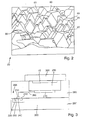
- FIG. 2 For example, an electron micrograph on a textured surface of the silicon substrate 20 immediately after the KOH etch is shown. This lacks both the thin-film layer 30 and the intermediate layer 40. The following are only the differences from the explanations in connection with the FIG. 1a cited. It shows the pyramidal structure, in addition to the tips now also platforms 60 of different sizes are formed.
- FIG. 12 is a schematic diagram of a CCFET transistor using an electrode with a layer structure of one of the embodiments in one of the FIG Figures 1a - Fig.1c , In the following, only the differences from the explanations in connection with the illustrations in the preceding figures are given.
- a MOS transistor 205 having a gate 210, a source 220 and a drain 230 is formed. Between source 220 and drain 230, a channel region 240 is arranged.
- the MOS transistor 205 is disposed in a well 250.
- the gate 210 is connected to a line 260 having a first electrode 270.
- a multilayer dielectric layer structure 280 is arranged on the upper side of the silicon wafer 200.
- the layer structure 280 forms a cavity 290.
- the first electrode 270 is disposed at the bottom surface of the cavity 290.
- the cavity is covered by a support structure 300.
- the support structure 300 has the layer system 10 on the underside, wherein the surface of the silicon substrate 20 down toward the first electrode 270.
- the layer system 10 forms a counter electrode to the first electrode 270. Both electrodes together form a capacitor. If the thin-film layer 30 has gas-sensitive properties, the potential at the surface of the layer system 10 of the capacitor facing the cavity 290 changes depending on the deposit of the capacitor, and this changes the conductivity of the channel region 240.
- the layer system 10 is a gas-sensitive control electrode in a CCFET Integrated gas sensor.
- FIG. 4 In the picture of the FIG. 4 is a cross-sectional view of a fourth embodiment of the invention layer structure with a textured intermediate layer is shown.
- the intermediate layer 40 likewise has a texturing, wherein the texture spacing is preferably between 0.1 ⁇ m to 1 ⁇ m and the depth of the texture is preferably between 0.1 ⁇ m to 1 ⁇ m.
- the texture pitch and the texture depth are each smaller than the texture pitch and the texture depth of the surface of the silicon substrate 20.
Landscapes
- Life Sciences & Earth Sciences (AREA)
- Chemical & Material Sciences (AREA)
- Health & Medical Sciences (AREA)
- Physics & Mathematics (AREA)
- Biochemistry (AREA)
- Microelectronics & Electronic Packaging (AREA)
- Chemical Kinetics & Catalysis (AREA)
- Electrochemistry (AREA)
- Engineering & Computer Science (AREA)
- Analytical Chemistry (AREA)
- Molecular Biology (AREA)
- General Health & Medical Sciences (AREA)
- General Physics & Mathematics (AREA)
- Immunology (AREA)
- Pathology (AREA)
- Investigating Or Analyzing Materials By The Use Of Fluid Adsorption Or Reactions (AREA)
- Weting (AREA)
- Physical Vapour Deposition (AREA)
- Other Surface Treatments For Metallic Materials (AREA)
Abstract
Description
- Die Erfindung betrifft ein Schichtsystem gemäß dem Oberbegriff des Patentanspruchs 1.
- Aus der
DE 689 24 140 T2 ist eine Dünnfilm-Sensorstruktur mit Platin auf Siliziumnitrid bekannt, wobei die Dünnfilmschicht aus Metalloxid auf der Siliziumnitridschicht angeordnet und die Dünnfilmschicht mit Platin abgedeckt ist. Ein Verfahren zur Herstellung von texturiertem Silizium ist aus derUS 4 137 123 B bekannt. Hierbei wird mit einer verdünnten KOH Ätzung die Oberfläche bearbeitet, um den Reflexionsgrad der Oberfläche zu verringern. Des Weiteren ist aus derEP 1 707 952 A1 ein in einen Gassensor integriertes Schichtsystem bekannt. - Vor diesem Hintergrund besteht die Aufgabe der Erfindung darin, eine Vorrichtung anzugeben, die den Stand der Technik weiterbildet.
- Die Aufgabe wird durch ein Schichtsystem mit den Merkmalen des Patentanspruchs 1 gelöst. Vorteilhafte Ausgestaltungen der Erfindung sind Gegenstand von Unteransprüchen.
- Gemäß dem Gegenstand der Erfindung wird ein Schichtsystem mit einem Schichtbereich bereitgestellt, wobei der Schichtbereich ein monokristallines Siliziumsubstrat mit einer Vorderseite und einer Rückseite aufweist und wobei auf der Vorderseite eine texturierte Oberfläche ausgebildet ist und die texturierte Oberfläche eine Topographie mit unterschiedlichen Höhen aufweist und auf der texturierten Oberfläche eine Dünnfilmschicht aus einem Metalloxid und / oder einer Oxidkeramik ausgebildet ist, wobei die Dünnfilmschicht die texturierte Oberfläche nur teilweise bedeckt. Es sei angemerkt, dass die Oberfläche aufgrund der Textur eine Mikrorauhigkeit aufweist und die Dünnfilmschicht sich an die Oberfläche der Textur anschmiegt, vorzugsweise konform, jedoch die Spitzen der Textur nicht bedeckt sind. Des Weiteren sei angemerkt, dass das Siliziumsubstrat vorzugsweise als Halbleiterwafer ausgebildet ist. Auf derartigen Siliziumwafer werden integrierte Schaltungen ausgebildet. Bevorzugt werden für die Ausbildung der texturierten Oberfläche genau die gleichen Halbleiterwafer verwendet wie im Falle der Herstellung einer integrierten Schaltung.
- Ein Vorteil der erfindungsgemäßen Vorrichtung ist es, dass das Siliziumsubstrat mit der texturierten Oberfläche eine derartige Oberflächenrauhigkeit aufweist, dass die Dünnfilmschicht mit der Unterlage eine kraftschlüssige Verbindung eingeht. Hierdurch wird es ermöglicht die spröden Dünnfilmschichten ohne eine Klebeverbindung mit der Siliziumoberfläche zu verbinden. Ein weiterer Vorteil ist, dass die Dünnfilmschichten eine große Oberfläche aufweisen. Hierbei ist es bevorzugt, dass die Dünnfilmschicht eine Dicke kleiner als die Tiefe der Texturierung aufweist.
- Untersuchungen der Anmelder haben gezeigt, dass es vorteilhaft ist, wenn die texturierte Oberfläche eine pyramidenförmige Topographie aufweist. In einer bevorzugten Ausführungsform sind die Seitenflächen der pyramidenförmige Textur als 111-Flächen ausgebildet. Ferner weist die Textur an der Oberseite 100-Flächen auf. Derartige pyramidenförmige Topographie lassen sich mit einer KOH Ätzung erzeugen.
- In der bevorzugten Ausbildung weist die texturierte Oberfläche dünnfilmschichtfreie Spitzen und / oder dünnfilmschichtfreie Plateaus auf, wobei die dünnfilm-schichtfreie Spitzen und / oder dünnfilmschichtfreie Plateaus die Oberfläche der Dünnfilmschicht in der Höhe überragen.
- In einer anderen Weiterbildung umfasst die Dünnfilmschicht einen Katalysator. Untersuchungen haben gezeigt, dass es vorteilhaft ist, als Katalysator Platin und / oder Palladium und / oder Rhodium zu verwenden.
- In einer Ausführungsform ist es bevorzugt, wenn zwischen der Dünnfilmschicht und der texturierten Oberfläche mindestens eine metallisch leitende Zwischenschicht ausgebildet ist und die texturierte Oberfläche teilweise oder vollständig von der metallisch leitenden Zwischenschicht bedeckt ist. Es versteht sich, dass auf der Oberfläche des Siliziumsubstrats die eine oder mehrere Zwischenschichten eine stoffschlüssige Verbindung mit der Oberfläche des Siliziumsubstrats ausbilden und hiernach die Dünnfilmschicht mit der obersten der Zwischenschichten eine stoffschlüssige Verbindung ausbildet. Demgemäß ist auf der texturierten Oberfläche des Siliziumsubstrates eine Abfolge von mindestens zwei Schichten ausgebildet.
- In einer Weiterbildung umfasst die metallisch leitende Zwischenschicht eine Silizidschicht, wobei es bevorzugt ist, dass die Silizidschicht Platin und / oder Titan und / oder Palladium umfasst. In einer weiteren Ausbildung ist die metallisch leitende Zwischenschicht elektrisch angeschlossen. In einer Ausführungsform ist zusätzlich oder anstelle der Zwischenschicht die Dünnfilmschicht elektrisch angeschlossen.
- Des Weiteren ist es bevorzugt, dass das texturierte Silizium in dem Schichtbereich eine p- oder eine n-Dotierung aufweist. Hierzu ist vorzugsweise in dem Schichtbereich eine n- oder p-Wanne ausgebildet.
- Vorteilhaft ist, den Schichtbereich als gassensitive Steuerelektrode in einen SGFET oder einen CCFET-Gassensor zu integrieren. Ferner hat es sich als vorteilhaft gezeigt, die Dünnfilmschicht aus Galliumoxid und / oder aus Zinnoxid und / oder aus Bariumtitanat und / oder aus Bariumcarbonat auszubilden.
- Vorteilhaft ist, wenn die texturierte Oberfläche Pyramidendeckflächen oder Pyramidenspitzen enthält und zwischen unmittelbar benachbarten Pyramidenspitzen oder Pyramidendeckflächen ein Abstand von 1 µm bis 10 µm ausgebildet ist und die Pyramidendeckflächen oder Pyramidenspitzen zwischen 1 µm und 10 µm hoch sind.
- In einer andern Ausführungsform weist die metallische Zwischenschicht eine Texturierung mit einem Texturabstand von 0,1 µm bis 1 µm und einer Texturtiefe von 0,1 µm bis 1 µm auf, wobei der Texturabstand und die Texturtiefe jeweils kleiner als die von der Oberfläche der Siliziumschicht sind.
- In einer Weiterbildung ist die Dünnfilmschicht polykristallin ausgebildet und die Korngrößen der Dünnfilmschicht sind kleiner als 2 µm.
- Die Erfindung wird nachfolgend unter Bezugnahme auf die Zeichnungen näher erläutert. Hierbei werden gleichartige Teile mit identischen Bezeichnungen beschriftet. Die dargestellte Ausführungsformen sind stark schematisiert, d.h. die Abstände und laterale und vertikale Erstreckung sind nicht maßstäblich und weisen, sofern nicht anders angegeben auch keine ableitbare geometrische Relation zueinander auf. Darin zeigen die:
- Figur 1a
- eine Querschnittsansicht auf eine erste erfindungsgemäße Ausführungsform des Schichtaufbaus,
- Figur 1b
- eine Querschnittsansicht auf eine zweite erfindungsgemäße Ausführungsform des Schichtaufbaus,
- Figur 1c
- eine Querschnittsansicht auf eine dritte erfindungsgemäße Ausführungsform des Schichtaufbaus,
- Figur 2
- eine elektronenmikroskopische Aufnahme auf eine texturierte Oberfläche eines Siliziumsubstrats,
- Figur 3
- eine Prinzipskizze eines CCFET-Transistors unter Verwendung einer Elektrode mit einem Schichtaufbaus einer der Ausführungsformen, dargestellt in der
Fig. 1a - Fig.1c , - Figur 4
- eine Querschnittsansicht auf eine vierte erfindungsgemäße Ausführungsform des Schichtaufbaus mit einer texturierten Zwischenschicht.
- Die Abbildung der
Figur 1a zeigt eine Querschnittsansicht einer ersten Ausführungsform eines Schichtsystems 10, aufweisend ein monokristallines Siliziumsubstrat 20, mit einer Vorderseite 22 und einer Rückseite 24. Auf der Vorderseite 22 des Siliziumsubstrats 20 ist eine texturierte Oberfläche ausgebildet. Hierbei weist die texturierte Oberfläche eine Topographie mit unter-schiedlichen Höhen auf. Es sei angemerkt, dass die Topographie eine Vielzahl von Erhebungen zeigt, wobei aus Gründen der Übersichtlichkeit die Erhebungen vereinfacht als Spitzen 26 dargestellt sind. Indem die Textur vorzugsweise mittels einer KOH-Ätzung erzeugt wird, ist die Topographie der texturierten Oberfläche pyramidenförmig, d.h. die Seitenflächen 28 der pyramidenförmige Erhebungen bzw. Spitzen 26 sind als 111-Flächen ausgebildet. Sofern die Erhebungen der Textur Plateaus ausbilden, sind an der Oberseite 100-Flächen - nicht dargestellt - ausgebildet. Es sei des Weiteren angemerkt, dass die Spitzen eine unterschiedliche Höhe aufweisen. Des Weiteren sind die Spitzen unterschiedlich zueinander entfernt. Bevorzugt ist, dass zwischen unmittelbar benachbarten Pyramidenspitzen oder Pyramidendeckflächen ein Abstand von 1 µm bis 10 µm ausgebildet ist und die Pyramidendeckflächen oder Pyramidenspitzen eine Höhe zwischen 1 µm und 10 µm bezogen auf den Fuß der Pyramide aufweisen. Ferner weist das Siliziumsubstrat 20, welche im Allgemeinen als Vorderseite eines Silizium-Halbleiterwafer ausgebildet ist, eine n- oder p-Dotierstoffkonzentration, vorzugsweise von Phosphor oder Bor, in einem Bereich von einigen 10e17 N/cm3 bis wenigen 10e19 N/cm3 auf. Es versteht sich, dass die monokristalline Schicht auch epitaktisch gewachsen sein kann. Das Siliziumsubstrat 20 ist zusätzlich oder anstelle der Dünnfilmschicht 30 elektrisch angeschlossen - nicht dargestellt. Ferner sei angemerkt, dass neben den dargestellten texturierten Gebieten auf der Siliziumsubstratschicht 20 auch nicht texturierte Gebiete - nicht dargestellt - ausgebildet sein können. Um solche Gebiete voneinander zu separieren, werden die bekannten photolithographischen Verfahren angewendet. - Auf der texturierten Oberfläche ist eine Dünnfilmschicht 30 aus einem Metalloxid und / oder einer Oxidkeramik ausgebildet, wobei die Dünnfilmschicht 30 die texturierte Oberfläche nur teilweise bedeckt und bevorzugt Galliumoxid und / oder Zinnoxid und / oder Bariumtitanat und / oder Bariumcarbonat enthält. Zusätzlich ist es vorteilhaft, wenn die Dünnfilmschicht 30 einen Katalysator umfasst. Besonders vorteilhaft ist es, wenn der Katalysator Platin und / oder Palladium und / oder Rhodium aufweist. Die Dünnfilmschicht 30 weist eine im Bereich der Metalle liegende Leitfähigkeit auf. Ferner ist die Dünnflmschicht elektrisch angeschlossen
- Es ist bevorzugt, dass die Dünnfilmschicht 30 an der dicksten Stelle eine Dicke kleiner als 10 µm aufweist, jedoch überragt ein Teil der Spitzen 26 oder der Plateaus die Oberfläche der Dünnfilmschicht 30 und sind nicht mit der Dünnfilmschicht 30 bedeckt. Vorzugsweise bildet die Dünnfilmschicht 30 eine stoffschlüssige Verbindung mit der Unterlage aus. Vorteilhaft ist, wenn die Dünnfilmschicht polykristallin ausgebildet ist und die Korngrößen der Dünnfilmschicht kleiner als 2 µm sind.
- In der Abbildung der
Figur 1b ist eine Querschnittsansicht einer zweiten Ausführungsform des Schichtsystems 10 dargestellt. Nachfolgend werden nur die Unterschiede zu den Erläuterungen in Zusammenhang mit derFigur 1a angeführt. Zwischen der Dünnfilmschicht 30 und der Oberfläche auf der Vorderseite 22 des Siliziumsubstrats 20 ist eine metallisch leitende Zwischenschicht 40 ausgebildet. Die Zwischenschicht 40 bedeckt die Oberfläche also auch die Spitzen des Siliziumsubstrats 20 vorzugsweise vollständig und konform. Die Zwischenschicht 40 bildet einerseits eine stoffschlüssige Verbindung mit der Unterlage, also mit der Oberfläche der Siliziumsubstratschicht 20 als auch eine stoffschlüssige Verbindung mit der auf der Zwischenschicht 40 aufliegenden Dünnfilmschicht 30 aus. - Es versteht sich, dass die metallisch leitende Zwischenschicht 40 elektrisch angeschlossen ist - nicht dargestellt. Der elektrische Anschluss der Zwischenschicht 40 kann zusätzlich oder alternativ zu den elektrischen Anschlüssen des Siliziumsubstrats 20 und / oder der Dünnfilmschicht 30 ausgebildet sein. Der elektrische Anschluss kann in den texturierten oder, falls vorhanden, nicht texturierten Gebieten des Siliziumsubstrats 20 ausgebildet sein. Vorzugsweise umfasst die metallisch leitende Zwischenschicht eine Silizidschicht aus Platin und / oder Wolfram und / oder Titan und / oder Palladium.
- In der Abbildung der
Figur 1c ist eine Querschnittsansicht einer dritten Ausführungsform des Schichtsystems 10 dargestellt. Nachfolgend werden nur die Unterschiede zu den Erläuterungen in Zusammenhang mit derFigur 1b angeführt. Die Texturierung der Oberfläche des Siliziumsubstrats 20 bildet nun eine regelmäßige Topographie aus. Aus der Oberfläche des Siliziumsubstrats 20 ragen zueinander gleichmäßig beabstandete Spitzen 26 heraus. Die Seitenflächen der Spitzen werden nicht notwendig von 111-Flächen gebildet. Zur Erzeugung der Spitzen 26 werden insbesondere photolithographische Verfahren, d. h. Maskenprozesse in Verbindung mit Trockenätzverfahren verwendet. - In der Abbildung der
Figur 2 ist eine elektronenmikroskopische Aufnahme auf eine texturierte Oberfläche des Siliziumsubstrats 20 unmittelbar nach der KOH-Ätzung dargestellt. Hierdurch fehlt sowohl die Dünnfilmschicht 30 als auch die Zwischenschicht 40. Folgenden werden nur die Unterschiede zu den Erläuterungen in Zusammenhang mit derFigur 1a angeführt. Es zeigt sich die pyramidenförmige Struktur, wobei neben den Spitzen nunmehr auch Plateaus 60 unterschiedlicher Größe ausgebildet sind. - In der Abbildung der
Figur 3 ist eine Prinzipskizze eines CCFET-Transistors dargestellt unter Verwendung einer Elektrode mit einem Schichtaufbau einer der Ausführungsformen in einer derFiguren 1a - Fig.1c . Im Folgenden werden nur die Unterschiede zu den Erläuterungen in Zusammenhang mit den Darstellungen in den vorangegangenen Figuren angeführt. In der Oberseite eines Siliziumwafers 200 ist ein MOS-Transistor 205 mit einem Gate 210, einem Source 220 und einer Drain 230 ausgebildet. Zwischen Source 220 und der Drain 230 ist ein Kanalgebiet 240 angeordnet. Der MOS-Transistor 205 ist einer Wanne 250 angeordnet. Das Gate 210 ist mit einer Leitung 260 mit einer ersten Elektrode 270 verschaltet. Auf der Oberseite des Siliziumwafers 200 ist ein mehrlagiger dielektrischer Schichtaufbau 280 angeordnet. Der Schichtaufbau 280 bildet eine Kavität 290 aus. An der Bodenfläche der Kavität 290 ist die erste Elektrode 270 angeordnet. Die Kavität wird bedeckt von einer Tragstruktur 300. Die Tragstruktur 300 weist an der Unterseite das Schichtsystem 10 auf, wobei die Oberfläche des Siliziumsubstrats 20 nach unten in Richtung der ersten Elektrode 270 zeigt. Das Schichtsystem 10 bildet eine Gegenelektrode zu der ersten Elektrode 270 aus. Beide Elektroden bilden zusammen einen Kondensator aus. Sofern die Dünnfilmschicht 30 gassensitive Eigenschaften aufweist, ändert sich je nach Anlagerung von bestimmten das Potential an der der Kavität 290 zugewandten Oberfläche des Schichtsystems 10 des Kondensators und hierdurch ändert sich die Leitfähigkeit des Kanalgebiets 240. Zusammengefasst ist das Schichtsystem 10 als gassensitive Steuerelektrode in einen CCFET-Gassensor integriert. - In der Abbildung der
Figur 4 ist eine Querschnittsansicht auf eine vierte erfindungsgemäße Ausführungsform des Schichtaufbaus mit einer texturierten Zwischenschicht dargestellt. Im Folgenden werden nur die Unterschiede zu den Erläuterungen in Zusammenhang mit der Darstellung der Ausführungsform derFigur 1b angeführt. Die Zwischenschicht 40 weist ebenfalls eine Texturierung auf, wobei der Texturabstand vorzugsweise zwischen 0,1 µm bis 1 µm und die Tiefe der Textur vorzugsweise zwischen 0,1 µm bis 1 µm beträgt. Jedenfalls sind der Texturabstand und die Texturtiefe jeweils kleiner als der Texturabstand und die Texturtiefe der Oberfläche des Siliziumsubstrats 20.
Claims (18)
- Schichtsystem (10) mit einem Schichtbereich, wobei der Schichtbereich aufweist,
ein monokristallines Siliziumsubstrat (20) mit einer Vorderseite (22) und einer Rückseite (24), wobei auf der Vorderseite (22) eine texturierte Oberfläche ausgebildet ist und die texturierte Oberfläche eine Topographie mit unterschiedlichen Höhen aufweist,
dadurch gekennzeichnet, dass
auf der texturierten Oberfläche eine Dünnfilmschicht (30) aus einem Metalloxid und / oder einer Oxidkeramik ausgebildet ist, wobei die Dünnfilmschicht (30) die texturierte Oberfläche nur teilweise bedeckt. - Schichtsystem (10) nach Anspruch 1, dadurch gekennzeichnet, dass die texturierte Oberfläche eine pyramidenförmige Topographie aufweist.
- Schichtsystem (10) nach Anspruch 1 oder Anspruch 2, dadurch gekennzeichnet, dass die texturierte Oberfläche dünnfilmschichtfreie Spitzen (26) und / oder dünnfilmschichtfreie Plateaus (60) aufweist und die dünnfilmschichtfreie Spitzen (26) und / oder dünnfilmschichtfreie Plateaus (60) die Oberfläche der Dünnfilmschicht (30) in der Höhe überragen.
- Schichtsystem (10) nach Anspruch 1 oder Anspruch 2, dadurch gekennzeichnet, dass die Dünnfilmschicht (30) einen Katalysator umfasst.
- Schichtsystem (10) nach Anspruch 4, dadurch gekennzeichnet, dass der Katalysator Platin und / oder Palladium und / oder Rhodium aufweist.
- Schichtsystem (10) nach einem der Ansprüche 1 bis 5, dadurch gekennzeichnet, dass die Dünnfilmschicht (30) eine Dicke kleiner als 10 µm aufweist.
- Schichtsystem (10) nach einem der Ansprüche 1 bis 6, dadurch gekennzeichnet, dass zwischen der Dünnfilmschicht (30) und der texturierten Oberfläche eine metallisch leitende Zwischenschicht (40) die texturierte Oberfläche teilweise oder vollständig bedeckt.
- Schichtsystem (10) nach Anspruch 7, dadurch gekennzeichnet, dass die metallisch leitende Zwischenschicht (40) eine Silizidschicht umfasst.
- Schichtsystem (10) nach Anspruch 8, dadurch gekennzeichnet, dass die Silizidschicht Platin und / oder Titan und / oder Palladium umfasst.
- Schichtsystem (10) nach einem der Ansprüche 7 bis 9, dadurch gekennzeichnet, dass die metallisch leitende Zwischenschicht (40) elektrisch angeschlossen ist.
- Schichtsystem (10) nach einem der vorstehenden Ansprüche, dadurch gekennzeichnet, dass die Dünnfilmschicht (30) elektrisch angeschlossen ist.
- Schichtsystem (10) nach einem der vorstehenden Ansprüche, dadurch gekennzeichnet, dass das texturierte Siliziumsubstrat (20) in dem Schichtbereich eine p- oder eine n-Dotierung aufweist.
- Schichtsystem (10) nach einem der vorstehenden Ansprüche, dadurch gekennzeichnet, dass der Schichtbereich als gassensitive Steuerelektrode in einen SGFET- oder einen CCFET-Gassensor integriert ist.
- Schichtsystem (10) nach einem der vorstehenden Ansprüche, dadurch gekennzeichnet, dass die Seitenflächen (28) der pyramidenförmige Textur 111-Flächen sind und die Textur an der Oberseite 100-Flächen aufweist.
- Schichtsystem (10) nach einem der vorstehenden Ansprüche, dadurch gekennzeichnet, dass die Dünnfilmschicht (30) Galliumoxid und / oder Zinnoxid und / oder Bariumtitanat und / oder Bariumcarbonat enthält.
- Schichtsystem (10) nach einem der vorstehenden Ansprüche, dadurch gekennzeichnet, dass die texturierte Oberfläche Pyramidendeckflächen oder Pyramidenspitzen enthält und zwischen unmittelbar benachbarten Pyramidenspitzen oder Pyramidendeckflächen ein Abstand von 1 µm bis 10 µm ausgebildet ist und die Pyramidendeckflächen oder Pyramidenspitzen zwischen 1 µm und 10 µm hoch sind.
- Schichtsystem (10) nach einem der vorstehenden Ansprüche, dadurch gekennzeichnet, dass die metallischen Zwischenschicht (40) eine Texturierung aufweist mit einem Texturabstand von 0,1 µm bis 1 µm und einer Texturtiefe von 0,1 µm bis 1 µm und der Texturabstand und die Texturtiefe jeweils kleiner als die an der Oberfläche des Siliziumsubstrats (20) ist.
- Schichtsystem (10) nach einem der vorstehenden Ansprüche, dadurch gekennzeichnet, dass die Dünnfilmschicht (30) polykristallin ausgebildet ist und die Korngrößen der Dünnfilmschicht (30) kleiner als 2 µm sind.
Applications Claiming Priority (1)
| Application Number | Priority Date | Filing Date | Title |
|---|---|---|---|
| DE102013016331.5A DE102013016331A1 (de) | 2013-10-05 | 2013-10-05 | Schichtsystem |
Publications (3)
| Publication Number | Publication Date |
|---|---|
| EP2857833A2 true EP2857833A2 (de) | 2015-04-08 |
| EP2857833A3 EP2857833A3 (de) | 2015-04-15 |
| EP2857833B1 EP2857833B1 (de) | 2017-04-12 |
Family
ID=51730293
Family Applications (1)
| Application Number | Title | Priority Date | Filing Date |
|---|---|---|---|
| EP14003406.7A Active EP2857833B1 (de) | 2013-10-05 | 2014-10-02 | Schichtsystem |
Country Status (3)
| Country | Link |
|---|---|
| US (1) | US9500620B2 (de) |
| EP (1) | EP2857833B1 (de) |
| DE (1) | DE102013016331A1 (de) |
Citations (3)
| Publication number | Priority date | Publication date | Assignee | Title |
|---|---|---|---|---|
| US4137123A (en) | 1975-12-31 | 1979-01-30 | Motorola, Inc. | Texture etching of silicon: method |
| DE68924140T2 (de) | 1988-12-23 | 1996-05-09 | Honeywell Inc | Adhäsionsschicht für auf Platin basierende Sensoren. |
| EP1707952A1 (de) | 2005-03-31 | 2006-10-04 | Micronas GmbH | Gassensitiver Feldeffekttransistor mit Luftspalt und Verfahren zu dessen Herstellung |
Family Cites Families (11)
| Publication number | Priority date | Publication date | Assignee | Title |
|---|---|---|---|---|
| JPH0731150B2 (ja) * | 1987-02-16 | 1995-04-10 | 日本碍子株式会社 | 酸素センサ素子及びその製造方法 |
| DE4444607C2 (de) * | 1994-12-14 | 1996-08-29 | Ignaz Prof Dr Eisele | Anpassung von Austrittsarbeits-Sensoren für oxidierende und reduzierende Gase an den Betrieb bei Umgebungstemperatur durch Einbau Feuchte-aufnehmender sensitiver Schichten |
| WO2004032197A2 (en) | 2002-10-03 | 2004-04-15 | Pan Jit Americas, Inc. | Low temperature texturing layer to enhance adhesion of subsequent layers |
| DE102004019638A1 (de) * | 2004-04-22 | 2005-11-17 | Siemens Ag | FET-basierter Sensor zur Detektion von insbesondere reduzierenden Gasen, Herstellungs- und Betriebsverfahren |
| US8710355B2 (en) * | 2008-12-22 | 2014-04-29 | E I Du Pont De Nemours And Company | Compositions and processes for forming photovoltaic devices |
| TW201030994A (en) * | 2009-02-12 | 2010-08-16 | Nexpower Technology Corp | Two sided light absorbing type solar cell |
| US8187971B2 (en) * | 2009-11-16 | 2012-05-29 | Tel Epion Inc. | Method to alter silicide properties using GCIB treatment |
| DE102009054435A1 (de) * | 2009-11-25 | 2011-05-26 | Kechter, Andreas, Dipl.-Ing. | Heizbarer Gassensor und Verfahren zu dessen Herstellung |
| DE102010025983A1 (de) * | 2010-03-03 | 2011-09-08 | Centrotherm Photovoltaics Ag | Solarzelle mit dielektrischer Rückseitenverspiegelung und Verfahren zu deren Herstellung |
| US9134270B2 (en) * | 2010-03-25 | 2015-09-15 | Stichting Imec Nederland | Amorphous thin film for sensing |
| DE102012022136B4 (de) | 2011-11-21 | 2014-01-23 | Micronas Gmbh | Halbleiter-Gassensor und Verfahren zur Messung eines Restgasanteils mit einem Halbleiter-Gassensor |
-
2013
- 2013-10-05 DE DE102013016331.5A patent/DE102013016331A1/de not_active Withdrawn
-
2014
- 2014-10-02 EP EP14003406.7A patent/EP2857833B1/de active Active
- 2014-10-06 US US14/507,428 patent/US9500620B2/en active Active
Patent Citations (3)
| Publication number | Priority date | Publication date | Assignee | Title |
|---|---|---|---|---|
| US4137123A (en) | 1975-12-31 | 1979-01-30 | Motorola, Inc. | Texture etching of silicon: method |
| DE68924140T2 (de) | 1988-12-23 | 1996-05-09 | Honeywell Inc | Adhäsionsschicht für auf Platin basierende Sensoren. |
| EP1707952A1 (de) | 2005-03-31 | 2006-10-04 | Micronas GmbH | Gassensitiver Feldeffekttransistor mit Luftspalt und Verfahren zu dessen Herstellung |
Also Published As
| Publication number | Publication date |
|---|---|
| US9500620B2 (en) | 2016-11-22 |
| EP2857833B1 (de) | 2017-04-12 |
| US20150096354A1 (en) | 2015-04-09 |
| EP2857833A3 (de) | 2015-04-15 |
| DE102013016331A1 (de) | 2015-04-09 |
Similar Documents
| Publication | Publication Date | Title |
|---|---|---|
| DE102014110650B4 (de) | Halbleitervorrichtung mit zelltrenchstrukturen und kontakten und verfahren zum herstellen einer halbleitervorrichtung | |
| DE102013112797B4 (de) | Anordnung mit halbleitervorrichtung einschliesslich eines chipträgers, halbleiterwafer und verfahren zum herstellen einer halbleitervorrichtung | |
| DE102011085331A1 (de) | Halbleitervorrichtung und Verfahren zum Herstellen derselben | |
| DE102016107203B4 (de) | Leistungshalbleiterbauelementgraben mit Feldplatte und Gateelektrode und Verfahren zur Herstellung | |
| DE102008051245A1 (de) | Hochvolttransistor mit hoher Stromtragfähigkeit und Verfahren zur Herstellung | |
| DE102009002813B4 (de) | Verfahren zur Herstellung eines Transistorbauelements mit einer Feldplatte | |
| DE102015103211B4 (de) | Verfahren zum herstellen einer halbleitervorrichtung mit ersten und zweiten feldelektrodenstrukturen | |
| DE102015111492B4 (de) | Bauelemente und Verfahren zur Herstellung von Bauelementen | |
| DE102014113115B4 (de) | Halbleitervorrichtung und verfahren zu deren herstellung | |
| DE102014206572B4 (de) | Siliziumcarbidhalbleitervorrichtung und herstellungsverfahren für dieselbe | |
| DE10224003B4 (de) | Halbleitervorrichtung und Verfahren für ihre Herstellung | |
| DE4320780A1 (de) | Halbleiteranordnung und Verfahren zur Herstellung | |
| DE102006017946B4 (de) | Siliziumkarbidhalbleitervorrichtung | |
| DE102010042606A1 (de) | Manufacturing method of semiconductor device | |
| DE102015206113A1 (de) | Verfahren zum bilden einer elektronischen vorrichtung, die ein abschlussgebiet mit einem isolatiionsgebiet aufweist | |
| EP0342274B1 (de) | Anordnung zur Verminderung von Piezoeffekten in mindestens einem in einem Halbleitermaterial angeordneten piezoeffekt-empfindlichen elektrischen Bauelement und Verfahren zur Herstellung dieser Anordnung | |
| EP2857832B1 (de) | Schichtsystem | |
| EP2857833B1 (de) | Schichtsystem | |
| DE112019007795T5 (de) | Halbleitervorrichtung | |
| DE102005008191B4 (de) | Verfahren zur Herstellung von VDMOS-Transistoren | |
| DE102014203075B4 (de) | Magnetsensor und Verfahren zu dessen Herstellung | |
| DE102016222913A1 (de) | Gassensor mit einem Halbleitersubstrat mit mindestens einer Isolationsschicht und einer Leiterbahn | |
| DE102018113573B4 (de) | Diode mit einem Halbleiterkörper | |
| DE1269732B (de) | Verfahren zum Herstellen von Halbleiteranordnungen | |
| DE102014103540B4 (de) | Halbleiterbauelement und integrierte schaltung |
Legal Events
| Date | Code | Title | Description |
|---|---|---|---|
| PUAL | Search report despatched |
Free format text: ORIGINAL CODE: 0009013 |
|
| PUAI | Public reference made under article 153(3) epc to a published international application that has entered the european phase |
Free format text: ORIGINAL CODE: 0009012 |
|
| 17P | Request for examination filed |
Effective date: 20141002 |
|
| AK | Designated contracting states |
Kind code of ref document: A2 Designated state(s): AL AT BE BG CH CY CZ DE DK EE ES FI FR GB GR HR HU IE IS IT LI LT LU LV MC MK MT NL NO PL PT RO RS SE SI SK SM TR |
|
| AX | Request for extension of the european patent |
Extension state: BA ME |
|
| AK | Designated contracting states |
Kind code of ref document: A3 Designated state(s): AL AT BE BG CH CY CZ DE DK EE ES FI FR GB GR HR HU IE IS IT LI LT LU LV MC MK MT NL NO PL PT RO RS SE SI SK SM TR |
|
| AX | Request for extension of the european patent |
Extension state: BA ME |
|
| RIC1 | Information provided on ipc code assigned before grant |
Ipc: G01N 27/414 20060101AFI20150312BHEP |
|
| R17P | Request for examination filed (corrected) |
Effective date: 20150811 |
|
| RBV | Designated contracting states (corrected) |
Designated state(s): AL AT BE BG CH CY CZ DE DK EE ES FI FR GB GR HR HU IE IS IT LI LT LU LV MC MK MT NL NO PL PT RO RS SE SI SK SM TR |
|
| 17Q | First examination report despatched |
Effective date: 20160309 |
|
| GRAP | Despatch of communication of intention to grant a patent |
Free format text: ORIGINAL CODE: EPIDOSNIGR1 |
|
| STAA | Information on the status of an ep patent application or granted ep patent |
Free format text: STATUS: GRANT OF PATENT IS INTENDED |
|
| INTG | Intention to grant announced |
Effective date: 20161104 |
|
| GRAJ | Information related to disapproval of communication of intention to grant by the applicant or resumption of examination proceedings by the epo deleted |
Free format text: ORIGINAL CODE: EPIDOSDIGR1 |
|
| GRAP | Despatch of communication of intention to grant a patent |
Free format text: ORIGINAL CODE: EPIDOSNIGR1 |
|
| INTG | Intention to grant announced |
Effective date: 20170105 |
|
| GRAS | Grant fee paid |
Free format text: ORIGINAL CODE: EPIDOSNIGR3 |
|
| GRAA | (expected) grant |
Free format text: ORIGINAL CODE: 0009210 |
|
| STAA | Information on the status of an ep patent application or granted ep patent |
Free format text: STATUS: THE PATENT HAS BEEN GRANTED |
|
| GRAT | Correction requested after decision to grant or after decision to maintain patent in amended form |
Free format text: ORIGINAL CODE: EPIDOSNCDEC |
|
| AK | Designated contracting states |
Kind code of ref document: B1 Designated state(s): AL AT BE BG CH CY CZ DE DK EE ES FI FR GB GR HR HU IE IS IT LI LT LU LV MC MK MT NL NO PL PT RO RS SE SI SK SM TR |
|
| RAP1 | Party data changed (applicant data changed or rights of an application transferred) |
Owner name: TDK-MICRONAS GMBH |
|
| REG | Reference to a national code |
Ref country code: GB Ref legal event code: FG4D Free format text: NOT ENGLISH |
|
| REG | Reference to a national code |
Ref country code: CH Ref legal event code: EP |
|
| REG | Reference to a national code |
Ref country code: IE Ref legal event code: FG4D Free format text: LANGUAGE OF EP DOCUMENT: GERMAN |
|
| REG | Reference to a national code |
Ref country code: AT Ref legal event code: REF Ref document number: 884410 Country of ref document: AT Kind code of ref document: T Effective date: 20170515 |
|
| REG | Reference to a national code |
Ref country code: DE Ref legal event code: R096 Ref document number: 502014003337 Country of ref document: DE |
|
| REG | Reference to a national code |
Ref country code: NL Ref legal event code: MP Effective date: 20170412 |
|
| REG | Reference to a national code |
Ref country code: LT Ref legal event code: MG4D |
|
| PG25 | Lapsed in a contracting state [announced via postgrant information from national office to epo] |
Ref country code: NL Free format text: LAPSE BECAUSE OF FAILURE TO SUBMIT A TRANSLATION OF THE DESCRIPTION OR TO PAY THE FEE WITHIN THE PRESCRIBED TIME-LIMIT Effective date: 20170412 |
|
| REG | Reference to a national code |
Ref country code: FR Ref legal event code: PLFP Year of fee payment: 4 |
|
| PG25 | Lapsed in a contracting state [announced via postgrant information from national office to epo] |
Ref country code: LT Free format text: LAPSE BECAUSE OF FAILURE TO SUBMIT A TRANSLATION OF THE DESCRIPTION OR TO PAY THE FEE WITHIN THE PRESCRIBED TIME-LIMIT Effective date: 20170412 Ref country code: FI Free format text: LAPSE BECAUSE OF FAILURE TO SUBMIT A TRANSLATION OF THE DESCRIPTION OR TO PAY THE FEE WITHIN THE PRESCRIBED TIME-LIMIT Effective date: 20170412 Ref country code: GR Free format text: LAPSE BECAUSE OF FAILURE TO SUBMIT A TRANSLATION OF THE DESCRIPTION OR TO PAY THE FEE WITHIN THE PRESCRIBED TIME-LIMIT Effective date: 20170713 Ref country code: HR Free format text: LAPSE BECAUSE OF FAILURE TO SUBMIT A TRANSLATION OF THE DESCRIPTION OR TO PAY THE FEE WITHIN THE PRESCRIBED TIME-LIMIT Effective date: 20170412 Ref country code: ES Free format text: LAPSE BECAUSE OF FAILURE TO SUBMIT A TRANSLATION OF THE DESCRIPTION OR TO PAY THE FEE WITHIN THE PRESCRIBED TIME-LIMIT Effective date: 20170412 Ref country code: NO Free format text: LAPSE BECAUSE OF FAILURE TO SUBMIT A TRANSLATION OF THE DESCRIPTION OR TO PAY THE FEE WITHIN THE PRESCRIBED TIME-LIMIT Effective date: 20170712 |
|
| PG25 | Lapsed in a contracting state [announced via postgrant information from national office to epo] |
Ref country code: BG Free format text: LAPSE BECAUSE OF FAILURE TO SUBMIT A TRANSLATION OF THE DESCRIPTION OR TO PAY THE FEE WITHIN THE PRESCRIBED TIME-LIMIT Effective date: 20170712 Ref country code: IS Free format text: LAPSE BECAUSE OF FAILURE TO SUBMIT A TRANSLATION OF THE DESCRIPTION OR TO PAY THE FEE WITHIN THE PRESCRIBED TIME-LIMIT Effective date: 20170812 Ref country code: SE Free format text: LAPSE BECAUSE OF FAILURE TO SUBMIT A TRANSLATION OF THE DESCRIPTION OR TO PAY THE FEE WITHIN THE PRESCRIBED TIME-LIMIT Effective date: 20170412 Ref country code: RS Free format text: LAPSE BECAUSE OF FAILURE TO SUBMIT A TRANSLATION OF THE DESCRIPTION OR TO PAY THE FEE WITHIN THE PRESCRIBED TIME-LIMIT Effective date: 20170412 Ref country code: LV Free format text: LAPSE BECAUSE OF FAILURE TO SUBMIT A TRANSLATION OF THE DESCRIPTION OR TO PAY THE FEE WITHIN THE PRESCRIBED TIME-LIMIT Effective date: 20170412 Ref country code: PL Free format text: LAPSE BECAUSE OF FAILURE TO SUBMIT A TRANSLATION OF THE DESCRIPTION OR TO PAY THE FEE WITHIN THE PRESCRIBED TIME-LIMIT Effective date: 20170412 |
|
| REG | Reference to a national code |
Ref country code: DE Ref legal event code: R097 Ref document number: 502014003337 Country of ref document: DE |
|
| PG25 | Lapsed in a contracting state [announced via postgrant information from national office to epo] |
Ref country code: DK Free format text: LAPSE BECAUSE OF FAILURE TO SUBMIT A TRANSLATION OF THE DESCRIPTION OR TO PAY THE FEE WITHIN THE PRESCRIBED TIME-LIMIT Effective date: 20170412 Ref country code: SK Free format text: LAPSE BECAUSE OF FAILURE TO SUBMIT A TRANSLATION OF THE DESCRIPTION OR TO PAY THE FEE WITHIN THE PRESCRIBED TIME-LIMIT Effective date: 20170412 Ref country code: EE Free format text: LAPSE BECAUSE OF FAILURE TO SUBMIT A TRANSLATION OF THE DESCRIPTION OR TO PAY THE FEE WITHIN THE PRESCRIBED TIME-LIMIT Effective date: 20170412 Ref country code: CZ Free format text: LAPSE BECAUSE OF FAILURE TO SUBMIT A TRANSLATION OF THE DESCRIPTION OR TO PAY THE FEE WITHIN THE PRESCRIBED TIME-LIMIT Effective date: 20170412 Ref country code: RO Free format text: LAPSE BECAUSE OF FAILURE TO SUBMIT A TRANSLATION OF THE DESCRIPTION OR TO PAY THE FEE WITHIN THE PRESCRIBED TIME-LIMIT Effective date: 20170412 |
|
| PLBE | No opposition filed within time limit |
Free format text: ORIGINAL CODE: 0009261 |
|
| STAA | Information on the status of an ep patent application or granted ep patent |
Free format text: STATUS: NO OPPOSITION FILED WITHIN TIME LIMIT |
|
| PG25 | Lapsed in a contracting state [announced via postgrant information from national office to epo] |
Ref country code: IT Free format text: LAPSE BECAUSE OF FAILURE TO SUBMIT A TRANSLATION OF THE DESCRIPTION OR TO PAY THE FEE WITHIN THE PRESCRIBED TIME-LIMIT Effective date: 20170412 Ref country code: SM Free format text: LAPSE BECAUSE OF FAILURE TO SUBMIT A TRANSLATION OF THE DESCRIPTION OR TO PAY THE FEE WITHIN THE PRESCRIBED TIME-LIMIT Effective date: 20170412 |
|
| 26N | No opposition filed |
Effective date: 20180115 |
|
| PG25 | Lapsed in a contracting state [announced via postgrant information from national office to epo] |
Ref country code: SI Free format text: LAPSE BECAUSE OF FAILURE TO SUBMIT A TRANSLATION OF THE DESCRIPTION OR TO PAY THE FEE WITHIN THE PRESCRIBED TIME-LIMIT Effective date: 20170412 Ref country code: MC Free format text: LAPSE BECAUSE OF FAILURE TO SUBMIT A TRANSLATION OF THE DESCRIPTION OR TO PAY THE FEE WITHIN THE PRESCRIBED TIME-LIMIT Effective date: 20170412 |
|
| REG | Reference to a national code |
Ref country code: IE Ref legal event code: MM4A |
|
| PG25 | Lapsed in a contracting state [announced via postgrant information from national office to epo] |
Ref country code: LU Free format text: LAPSE BECAUSE OF NON-PAYMENT OF DUE FEES Effective date: 20171002 |
|
| REG | Reference to a national code |
Ref country code: BE Ref legal event code: MM Effective date: 20171031 |
|
| PG25 | Lapsed in a contracting state [announced via postgrant information from national office to epo] |
Ref country code: BE Free format text: LAPSE BECAUSE OF NON-PAYMENT OF DUE FEES Effective date: 20171031 |
|
| PG25 | Lapsed in a contracting state [announced via postgrant information from national office to epo] |
Ref country code: MT Free format text: LAPSE BECAUSE OF FAILURE TO SUBMIT A TRANSLATION OF THE DESCRIPTION OR TO PAY THE FEE WITHIN THE PRESCRIBED TIME-LIMIT Effective date: 20170412 |
|
| REG | Reference to a national code |
Ref country code: FR Ref legal event code: PLFP Year of fee payment: 5 |
|
| PG25 | Lapsed in a contracting state [announced via postgrant information from national office to epo] |
Ref country code: IE Free format text: LAPSE BECAUSE OF NON-PAYMENT OF DUE FEES Effective date: 20171002 |
|
| PG25 | Lapsed in a contracting state [announced via postgrant information from national office to epo] |
Ref country code: HU Free format text: LAPSE BECAUSE OF FAILURE TO SUBMIT A TRANSLATION OF THE DESCRIPTION OR TO PAY THE FEE WITHIN THE PRESCRIBED TIME-LIMIT; INVALID AB INITIO Effective date: 20141002 |
|
| PG25 | Lapsed in a contracting state [announced via postgrant information from national office to epo] |
Ref country code: CY Free format text: LAPSE BECAUSE OF FAILURE TO SUBMIT A TRANSLATION OF THE DESCRIPTION OR TO PAY THE FEE WITHIN THE PRESCRIBED TIME-LIMIT Effective date: 20170412 |
|
| PG25 | Lapsed in a contracting state [announced via postgrant information from national office to epo] |
Ref country code: MK Free format text: LAPSE BECAUSE OF FAILURE TO SUBMIT A TRANSLATION OF THE DESCRIPTION OR TO PAY THE FEE WITHIN THE PRESCRIBED TIME-LIMIT Effective date: 20170412 |
|
| PG25 | Lapsed in a contracting state [announced via postgrant information from national office to epo] |
Ref country code: TR Free format text: LAPSE BECAUSE OF FAILURE TO SUBMIT A TRANSLATION OF THE DESCRIPTION OR TO PAY THE FEE WITHIN THE PRESCRIBED TIME-LIMIT Effective date: 20170412 |
|
| PG25 | Lapsed in a contracting state [announced via postgrant information from national office to epo] |
Ref country code: PT Free format text: LAPSE BECAUSE OF FAILURE TO SUBMIT A TRANSLATION OF THE DESCRIPTION OR TO PAY THE FEE WITHIN THE PRESCRIBED TIME-LIMIT Effective date: 20170412 |
|
| PG25 | Lapsed in a contracting state [announced via postgrant information from national office to epo] |
Ref country code: AL Free format text: LAPSE BECAUSE OF FAILURE TO SUBMIT A TRANSLATION OF THE DESCRIPTION OR TO PAY THE FEE WITHIN THE PRESCRIBED TIME-LIMIT Effective date: 20170412 |
|
| REG | Reference to a national code |
Ref country code: AT Ref legal event code: MM01 Ref document number: 884410 Country of ref document: AT Kind code of ref document: T Effective date: 20191002 |
|
| PG25 | Lapsed in a contracting state [announced via postgrant information from national office to epo] |
Ref country code: AT Free format text: LAPSE BECAUSE OF NON-PAYMENT OF DUE FEES Effective date: 20191002 |
|
| PGFP | Annual fee paid to national office [announced via postgrant information from national office to epo] |
Ref country code: GB Payment date: 20201022 Year of fee payment: 7 Ref country code: FR Payment date: 20201022 Year of fee payment: 7 Ref country code: CH Payment date: 20201021 Year of fee payment: 7 |
|
| REG | Reference to a national code |
Ref country code: CH Ref legal event code: PL |
|
| GBPC | Gb: european patent ceased through non-payment of renewal fee |
Effective date: 20211002 |
|
| PG25 | Lapsed in a contracting state [announced via postgrant information from national office to epo] |
Ref country code: GB Free format text: LAPSE BECAUSE OF NON-PAYMENT OF DUE FEES Effective date: 20211002 |
|
| PG25 | Lapsed in a contracting state [announced via postgrant information from national office to epo] |
Ref country code: LI Free format text: LAPSE BECAUSE OF NON-PAYMENT OF DUE FEES Effective date: 20211031 Ref country code: CH Free format text: LAPSE BECAUSE OF NON-PAYMENT OF DUE FEES Effective date: 20211031 |
|
| PG25 | Lapsed in a contracting state [announced via postgrant information from national office to epo] |
Ref country code: FR Free format text: LAPSE BECAUSE OF NON-PAYMENT OF DUE FEES Effective date: 20211031 |
|
| PGFP | Annual fee paid to national office [announced via postgrant information from national office to epo] |
Ref country code: DE Payment date: 20251021 Year of fee payment: 12 |