EP2853567A1 - Solar cells produced from high ohmic wafers and paste comprising Ag metal-oxide additive - Google Patents
Solar cells produced from high ohmic wafers and paste comprising Ag metal-oxide additive Download PDFInfo
- Publication number
- EP2853567A1 EP2853567A1 EP13004690.7A EP13004690A EP2853567A1 EP 2853567 A1 EP2853567 A1 EP 2853567A1 EP 13004690 A EP13004690 A EP 13004690A EP 2853567 A1 EP2853567 A1 EP 2853567A1
- Authority
- EP
- European Patent Office
- Prior art keywords
- paste
- metal
- preferred
- range
- wafer
- Prior art date
- Legal status (The legal status is an assumption and is not a legal conclusion. Google has not performed a legal analysis and makes no representation as to the accuracy of the status listed.)
- Withdrawn
Links
- 229910044991 metal oxide Inorganic materials 0.000 title claims abstract description 39
- 229910052709 silver Inorganic materials 0.000 title claims abstract description 21
- 239000000654 additive Substances 0.000 title abstract description 23
- 235000012431 wafers Nutrition 0.000 title description 74
- 230000000996 additive effect Effects 0.000 title description 3
- 150000004706 metal oxides Chemical class 0.000 title 1
- 229910052751 metal Inorganic materials 0.000 claims abstract description 40
- 239000002184 metal Substances 0.000 claims abstract description 38
- 239000002245 particle Substances 0.000 claims abstract description 35
- 239000011521 glass Substances 0.000 claims abstract description 30
- 238000000034 method Methods 0.000 claims abstract description 27
- 239000002243 precursor Substances 0.000 claims abstract description 26
- 239000000470 constituent Substances 0.000 claims abstract description 16
- 238000002360 preparation method Methods 0.000 claims abstract description 9
- 239000004065 semiconductor Substances 0.000 claims abstract description 6
- QVGXLLKOCUKJST-UHFFFAOYSA-N atomic oxygen Chemical compound [O] QVGXLLKOCUKJST-UHFFFAOYSA-N 0.000 claims abstract description 5
- 229910052760 oxygen Inorganic materials 0.000 claims abstract description 5
- 239000001301 oxygen Substances 0.000 claims abstract description 5
- 238000010304 firing Methods 0.000 claims description 44
- 239000000758 substrate Substances 0.000 claims description 36
- -1 Ag+ ions Chemical class 0.000 claims description 14
- 229910052721 tungsten Inorganic materials 0.000 claims description 9
- 229910052720 vanadium Inorganic materials 0.000 claims description 8
- 229910052725 zinc Inorganic materials 0.000 claims description 8
- 229910017988 AgVO3 Inorganic materials 0.000 claims description 7
- 229910015667 MoO4 Inorganic materials 0.000 claims description 7
- 229910052787 antimony Inorganic materials 0.000 claims description 7
- 229910052804 chromium Inorganic materials 0.000 claims description 6
- 229910052748 manganese Inorganic materials 0.000 claims description 6
- 229910052750 molybdenum Inorganic materials 0.000 claims description 6
- 229910052758 niobium Inorganic materials 0.000 claims description 6
- 229910052714 tellurium Inorganic materials 0.000 claims description 6
- 230000003647 oxidation Effects 0.000 claims description 5
- 238000007254 oxidation reaction Methods 0.000 claims description 5
- 229910014235 MyOz Inorganic materials 0.000 claims description 4
- 238000002844 melting Methods 0.000 claims description 4
- 230000008018 melting Effects 0.000 claims description 4
- 239000010410 layer Substances 0.000 description 132
- 210000004027 cell Anatomy 0.000 description 87
- 239000013528 metallic particle Substances 0.000 description 32
- 239000002019 doping agent Substances 0.000 description 29
- 239000000203 mixture Substances 0.000 description 27
- 239000003981 vehicle Substances 0.000 description 24
- 238000000576 coating method Methods 0.000 description 21
- 239000000463 material Substances 0.000 description 21
- 238000005259 measurement Methods 0.000 description 19
- 239000011230 binding agent Substances 0.000 description 18
- 238000002161 passivation Methods 0.000 description 18
- 239000002904 solvent Substances 0.000 description 16
- BQCADISMDOOEFD-UHFFFAOYSA-N Silver Chemical compound [Ag] BQCADISMDOOEFD-UHFFFAOYSA-N 0.000 description 14
- 229920000642 polymer Polymers 0.000 description 14
- 239000000523 sample Substances 0.000 description 14
- 239000004332 silver Substances 0.000 description 14
- 125000000217 alkyl group Chemical group 0.000 description 13
- 238000005245 sintering Methods 0.000 description 13
- 239000004094 surface-active agent Substances 0.000 description 13
- 239000000956 alloy Substances 0.000 description 11
- 229910045601 alloy Inorganic materials 0.000 description 11
- 239000011248 coating agent Substances 0.000 description 11
- 150000001875 compounds Chemical class 0.000 description 11
- 230000009477 glass transition Effects 0.000 description 11
- 150000002739 metals Chemical class 0.000 description 11
- 229910052782 aluminium Inorganic materials 0.000 description 10
- 238000005530 etching Methods 0.000 description 10
- 230000002349 favourable effect Effects 0.000 description 10
- 238000007639 printing Methods 0.000 description 10
- LYCAIKOWRPUZTN-UHFFFAOYSA-N Ethylene glycol Chemical compound OCCO LYCAIKOWRPUZTN-UHFFFAOYSA-N 0.000 description 9
- 125000000524 functional group Chemical group 0.000 description 9
- 229910052710 silicon Inorganic materials 0.000 description 9
- 238000012360 testing method Methods 0.000 description 8
- 239000007787 solid Substances 0.000 description 7
- 229910052581 Si3N4 Inorganic materials 0.000 description 6
- 239000004411 aluminium Substances 0.000 description 6
- XAGFODPZIPBFFR-UHFFFAOYSA-N aluminium Chemical compound [Al] XAGFODPZIPBFFR-UHFFFAOYSA-N 0.000 description 6
- 238000005538 encapsulation Methods 0.000 description 6
- 239000000126 substance Substances 0.000 description 6
- 238000010998 test method Methods 0.000 description 6
- XUIMIQQOPSSXEZ-UHFFFAOYSA-N Silicon Chemical compound [Si] XUIMIQQOPSSXEZ-UHFFFAOYSA-N 0.000 description 5
- 125000000484 butyl group Chemical group [H]C([*])([H])C([H])([H])C([H])([H])C([H])([H])[H] 0.000 description 5
- 239000010949 copper Substances 0.000 description 5
- 125000004185 ester group Chemical group 0.000 description 5
- 239000000049 pigment Substances 0.000 description 5
- BASFCYQUMIYNBI-UHFFFAOYSA-N platinum Substances [Pt] BASFCYQUMIYNBI-UHFFFAOYSA-N 0.000 description 5
- 125000001436 propyl group Chemical group [H]C([*])([H])C([H])([H])C([H])([H])[H] 0.000 description 5
- 239000010703 silicon Substances 0.000 description 5
- 230000003746 surface roughness Effects 0.000 description 5
- ZZSNKZQZMQGXPY-UHFFFAOYSA-N Ethyl cellulose Chemical compound CCOCC1OC(OC)C(OCC)C(OCC)C1OC1C(O)C(O)C(OC)C(CO)O1 ZZSNKZQZMQGXPY-UHFFFAOYSA-N 0.000 description 4
- VYPSYNLAJGMNEJ-UHFFFAOYSA-N Silicium dioxide Chemical compound O=[Si]=O VYPSYNLAJGMNEJ-UHFFFAOYSA-N 0.000 description 4
- 229910004273 TeO3 Inorganic materials 0.000 description 4
- GWEVSGVZZGPLCZ-UHFFFAOYSA-N Titan oxide Chemical compound O=[Ti]=O GWEVSGVZZGPLCZ-UHFFFAOYSA-N 0.000 description 4
- PNEYBMLMFCGWSK-UHFFFAOYSA-N aluminium oxide Inorganic materials [O-2].[O-2].[O-2].[Al+3].[Al+3] PNEYBMLMFCGWSK-UHFFFAOYSA-N 0.000 description 4
- 125000003118 aryl group Chemical group 0.000 description 4
- 229920002678 cellulose Polymers 0.000 description 4
- GHVNFZFCNZKVNT-UHFFFAOYSA-N decanoic acid Chemical compound CCCCCCCCCC(O)=O GHVNFZFCNZKVNT-UHFFFAOYSA-N 0.000 description 4
- 238000006073 displacement reaction Methods 0.000 description 4
- POULHZVOKOAJMA-UHFFFAOYSA-N dodecanoic acid Chemical compound CCCCCCCCCCCC(O)=O POULHZVOKOAJMA-UHFFFAOYSA-N 0.000 description 4
- 125000001033 ether group Chemical group 0.000 description 4
- 125000001495 ethyl group Chemical group [H]C([H])([H])C([H])([H])* 0.000 description 4
- IPCSVZSSVZVIGE-UHFFFAOYSA-N hexadecanoic acid Chemical compound CCCCCCCCCCCCCCCC(O)=O IPCSVZSSVZVIGE-UHFFFAOYSA-N 0.000 description 4
- 229910052909 inorganic silicate Inorganic materials 0.000 description 4
- 229910052745 lead Inorganic materials 0.000 description 4
- 125000002496 methyl group Chemical group [H]C([H])([H])* 0.000 description 4
- 239000000178 monomer Substances 0.000 description 4
- 229910052575 non-oxide ceramic Inorganic materials 0.000 description 4
- 239000011225 non-oxide ceramic Substances 0.000 description 4
- 230000000737 periodic effect Effects 0.000 description 4
- 239000000843 powder Substances 0.000 description 4
- 239000011347 resin Substances 0.000 description 4
- 229920005989 resin Polymers 0.000 description 4
- HQVNEWCFYHHQES-UHFFFAOYSA-N silicon nitride Chemical compound N12[Si]34N5[Si]62N3[Si]51N64 HQVNEWCFYHHQES-UHFFFAOYSA-N 0.000 description 4
- 239000013008 thixotropic agent Substances 0.000 description 4
- 229910052718 tin Inorganic materials 0.000 description 4
- QTBSBXVTEAMEQO-UHFFFAOYSA-N Acetic acid Chemical compound CC(O)=O QTBSBXVTEAMEQO-UHFFFAOYSA-N 0.000 description 3
- 239000001856 Ethyl cellulose Substances 0.000 description 3
- 229910004205 SiNX Inorganic materials 0.000 description 3
- WNLRTRBMVRJNCN-UHFFFAOYSA-N adipic acid Chemical compound OC(=O)CCCCC(O)=O WNLRTRBMVRJNCN-UHFFFAOYSA-N 0.000 description 3
- WUOACPNHFRMFPN-UHFFFAOYSA-N alpha-terpineol Chemical compound CC1=CCC(C(C)(C)O)CC1 WUOACPNHFRMFPN-UHFFFAOYSA-N 0.000 description 3
- 229910052785 arsenic Inorganic materials 0.000 description 3
- 230000015572 biosynthetic process Effects 0.000 description 3
- 229910052795 boron group element Inorganic materials 0.000 description 3
- 239000001913 cellulose Substances 0.000 description 3
- 229920001577 copolymer Polymers 0.000 description 3
- 229910052802 copper Inorganic materials 0.000 description 3
- 239000013078 crystal Substances 0.000 description 3
- 125000004122 cyclic group Chemical group 0.000 description 3
- 238000000407 epitaxy Methods 0.000 description 3
- 150000002148 esters Chemical class 0.000 description 3
- 229920001249 ethyl cellulose Polymers 0.000 description 3
- 235000019325 ethyl cellulose Nutrition 0.000 description 3
- 229940093476 ethylene glycol Drugs 0.000 description 3
- 125000005842 heteroatom Chemical group 0.000 description 3
- 125000004430 oxygen atom Chemical group O* 0.000 description 3
- 125000001147 pentyl group Chemical group C(CCCC)* 0.000 description 3
- 229910052697 platinum Inorganic materials 0.000 description 3
- 229910052696 pnictogen Inorganic materials 0.000 description 3
- 229920001223 polyethylene glycol Polymers 0.000 description 3
- 150000008163 sugars Chemical class 0.000 description 3
- 239000000725 suspension Substances 0.000 description 3
- 229940116411 terpineol Drugs 0.000 description 3
- DAFHKNAQFPVRKR-UHFFFAOYSA-N (3-hydroxy-2,2,4-trimethylpentyl) 2-methylpropanoate Chemical compound CC(C)C(O)C(C)(C)COC(=O)C(C)C DAFHKNAQFPVRKR-UHFFFAOYSA-N 0.000 description 2
- WRIDQFICGBMAFQ-UHFFFAOYSA-N (E)-8-Octadecenoic acid Natural products CCCCCCCCCC=CCCCCCCC(O)=O WRIDQFICGBMAFQ-UHFFFAOYSA-N 0.000 description 2
- BNRRFUKDMGDNNT-JQIJEIRASA-N (e)-16-methylheptadec-2-enoic acid Chemical compound CC(C)CCCCCCCCCCCC\C=C\C(O)=O BNRRFUKDMGDNNT-JQIJEIRASA-N 0.000 description 2
- OAYXUHPQHDHDDZ-UHFFFAOYSA-N 2-(2-butoxyethoxy)ethanol Chemical compound CCCCOCCOCCO OAYXUHPQHDHDDZ-UHFFFAOYSA-N 0.000 description 2
- GZMAAYIALGURDQ-UHFFFAOYSA-N 2-(2-hexoxyethoxy)ethanol Chemical compound CCCCCCOCCOCCO GZMAAYIALGURDQ-UHFFFAOYSA-N 0.000 description 2
- TWJNQYPJQDRXPH-UHFFFAOYSA-N 2-cyanobenzohydrazide Chemical compound NNC(=O)C1=CC=CC=C1C#N TWJNQYPJQDRXPH-UHFFFAOYSA-N 0.000 description 2
- LQJBNNIYVWPHFW-UHFFFAOYSA-N 20:1omega9c fatty acid Natural products CCCCCCCCCCC=CCCCCCCCC(O)=O LQJBNNIYVWPHFW-UHFFFAOYSA-N 0.000 description 2
- QSBYPNXLFMSGKH-UHFFFAOYSA-N 9-Heptadecensaeure Natural products CCCCCCCC=CCCCCCCCC(O)=O QSBYPNXLFMSGKH-UHFFFAOYSA-N 0.000 description 2
- 229910017083 AlN Inorganic materials 0.000 description 2
- IJGRMHOSHXDMSA-UHFFFAOYSA-N Atomic nitrogen Chemical compound N#N IJGRMHOSHXDMSA-UHFFFAOYSA-N 0.000 description 2
- QYEXBYZXHDUPRC-UHFFFAOYSA-N B#[Ti]#B Chemical compound B#[Ti]#B QYEXBYZXHDUPRC-UHFFFAOYSA-N 0.000 description 2
- 239000005632 Capric acid (CAS 334-48-5) Substances 0.000 description 2
- 239000005639 Lauric acid Substances 0.000 description 2
- OYHQOLUKZRVURQ-HZJYTTRNSA-N Linoleic acid Chemical compound CCCCC\C=C/C\C=C/CCCCCCCC(O)=O OYHQOLUKZRVURQ-HZJYTTRNSA-N 0.000 description 2
- 235000021360 Myristic acid Nutrition 0.000 description 2
- TUNFSRHWOTWDNC-UHFFFAOYSA-N Myristic acid Natural products CCCCCCCCCCCCCC(O)=O TUNFSRHWOTWDNC-UHFFFAOYSA-N 0.000 description 2
- 239000005642 Oleic acid Substances 0.000 description 2
- ZQPPMHVWECSIRJ-UHFFFAOYSA-N Oleic acid Natural products CCCCCCCCC=CCCCCCCCC(O)=O ZQPPMHVWECSIRJ-UHFFFAOYSA-N 0.000 description 2
- 235000021314 Palmitic acid Nutrition 0.000 description 2
- 239000004952 Polyamide Substances 0.000 description 2
- 239000002202 Polyethylene glycol Substances 0.000 description 2
- 229910020489 SiO3 Inorganic materials 0.000 description 2
- 235000021355 Stearic acid Nutrition 0.000 description 2
- 229910000831 Steel Inorganic materials 0.000 description 2
- 229910033181 TiB2 Inorganic materials 0.000 description 2
- 238000002441 X-ray diffraction Methods 0.000 description 2
- 239000002253 acid Substances 0.000 description 2
- 150000001298 alcohols Chemical class 0.000 description 2
- 229940053200 antiepileptics fatty acid derivative Drugs 0.000 description 2
- 229910052797 bismuth Inorganic materials 0.000 description 2
- 229910052796 boron Inorganic materials 0.000 description 2
- 150000001735 carboxylic acids Chemical class 0.000 description 2
- 239000000919 ceramic Substances 0.000 description 2
- 230000000052 comparative effect Effects 0.000 description 2
- 230000001143 conditioned effect Effects 0.000 description 2
- 238000012937 correction Methods 0.000 description 2
- SQIFACVGCPWBQZ-UHFFFAOYSA-N delta-terpineol Natural products CC(C)(O)C1CCC(=C)CC1 SQIFACVGCPWBQZ-UHFFFAOYSA-N 0.000 description 2
- 239000002270 dispersing agent Substances 0.000 description 2
- 239000003995 emulsifying agent Substances 0.000 description 2
- 239000000839 emulsion Substances 0.000 description 2
- 150000002170 ethers Chemical class 0.000 description 2
- 239000007789 gas Substances 0.000 description 2
- 229910052732 germanium Inorganic materials 0.000 description 2
- 229910052737 gold Inorganic materials 0.000 description 2
- 239000010931 gold Substances 0.000 description 2
- 229910021478 group 5 element Inorganic materials 0.000 description 2
- 229910021476 group 6 element Inorganic materials 0.000 description 2
- 238000010438 heat treatment Methods 0.000 description 2
- 125000004051 hexyl group Chemical group [H]C([H])([H])C([H])([H])C([H])([H])C([H])([H])C([H])([H])C([H])([H])* 0.000 description 2
- 230000001788 irregular Effects 0.000 description 2
- QXJSBBXBKPUZAA-UHFFFAOYSA-N isooleic acid Natural products CCCCCCCC=CCCCCCCCCC(O)=O QXJSBBXBKPUZAA-UHFFFAOYSA-N 0.000 description 2
- 230000031700 light absorption Effects 0.000 description 2
- 235000020778 linoleic acid Nutrition 0.000 description 2
- OYHQOLUKZRVURQ-IXWMQOLASA-N linoleic acid Natural products CCCCC\C=C/C\C=C\CCCCCCCC(O)=O OYHQOLUKZRVURQ-IXWMQOLASA-N 0.000 description 2
- 239000007788 liquid Substances 0.000 description 2
- 238000004519 manufacturing process Methods 0.000 description 2
- 229910003465 moissanite Inorganic materials 0.000 description 2
- 229910021421 monocrystalline silicon Inorganic materials 0.000 description 2
- WQEPLUUGTLDZJY-UHFFFAOYSA-N n-Pentadecanoic acid Natural products CCCCCCCCCCCCCCC(O)=O WQEPLUUGTLDZJY-UHFFFAOYSA-N 0.000 description 2
- 229910052759 nickel Inorganic materials 0.000 description 2
- 150000004767 nitrides Chemical class 0.000 description 2
- 229910052757 nitrogen Inorganic materials 0.000 description 2
- 125000002457 octadec-9-ynoyl group Chemical group C(CCCCCCCC#CCCCCCCCC)(=O)* 0.000 description 2
- QIQXTHQIDYTFRH-UHFFFAOYSA-N octadecanoic acid Chemical compound CCCCCCCCCCCCCCCCCC(O)=O QIQXTHQIDYTFRH-UHFFFAOYSA-N 0.000 description 2
- OQCDKBAXFALNLD-UHFFFAOYSA-N octadecanoic acid Natural products CCCCCCCC(C)CCCCCCCCC(O)=O OQCDKBAXFALNLD-UHFFFAOYSA-N 0.000 description 2
- ZQPPMHVWECSIRJ-KTKRTIGZSA-N oleic acid Chemical compound CCCCCCCC\C=C/CCCCCCCC(O)=O ZQPPMHVWECSIRJ-KTKRTIGZSA-N 0.000 description 2
- 229910052763 palladium Inorganic materials 0.000 description 2
- 229920001568 phenolic resin Polymers 0.000 description 2
- 239000005011 phenolic resin Substances 0.000 description 2
- 229910052698 phosphorus Inorganic materials 0.000 description 2
- 238000005334 plasma enhanced chemical vapour deposition Methods 0.000 description 2
- 238000000623 plasma-assisted chemical vapour deposition Methods 0.000 description 2
- 229920003229 poly(methyl methacrylate) Polymers 0.000 description 2
- 229920002647 polyamide Polymers 0.000 description 2
- 229920000515 polycarbonate Polymers 0.000 description 2
- 239000004417 polycarbonate Substances 0.000 description 2
- 229910021420 polycrystalline silicon Inorganic materials 0.000 description 2
- 229920000728 polyester Polymers 0.000 description 2
- 229920000570 polyether Chemical group 0.000 description 2
- 229920000193 polymethacrylate Polymers 0.000 description 2
- 239000004926 polymethyl methacrylate Substances 0.000 description 2
- 229920002635 polyurethane Chemical class 0.000 description 2
- 239000004814 polyurethane Chemical class 0.000 description 2
- 229920000036 polyvinylpyrrolidone Polymers 0.000 description 2
- 239000001267 polyvinylpyrrolidone Substances 0.000 description 2
- 235000013855 polyvinylpyrrolidone Nutrition 0.000 description 2
- 238000005215 recombination Methods 0.000 description 2
- 230000006798 recombination Effects 0.000 description 2
- 238000007650 screen-printing Methods 0.000 description 2
- 229910052711 selenium Inorganic materials 0.000 description 2
- 229910010271 silicon carbide Inorganic materials 0.000 description 2
- 239000000377 silicon dioxide Substances 0.000 description 2
- 239000010944 silver (metal) Substances 0.000 description 2
- 239000000243 solution Substances 0.000 description 2
- 239000003381 stabilizer Substances 0.000 description 2
- 239000008117 stearic acid Substances 0.000 description 2
- 239000010959 steel Substances 0.000 description 2
- 150000003509 tertiary alcohols Chemical class 0.000 description 2
- 239000002562 thickening agent Substances 0.000 description 2
- 239000010936 titanium Substances 0.000 description 2
- 238000012546 transfer Methods 0.000 description 2
- LNAZSHAWQACDHT-XIYTZBAFSA-N (2r,3r,4s,5r,6s)-4,5-dimethoxy-2-(methoxymethyl)-3-[(2s,3r,4s,5r,6r)-3,4,5-trimethoxy-6-(methoxymethyl)oxan-2-yl]oxy-6-[(2r,3r,4s,5r,6r)-4,5,6-trimethoxy-2-(methoxymethyl)oxan-3-yl]oxyoxane Chemical compound CO[C@@H]1[C@@H](OC)[C@H](OC)[C@@H](COC)O[C@H]1O[C@H]1[C@H](OC)[C@@H](OC)[C@H](O[C@H]2[C@@H]([C@@H](OC)[C@H](OC)O[C@@H]2COC)OC)O[C@@H]1COC LNAZSHAWQACDHT-XIYTZBAFSA-N 0.000 description 1
- VXQBJTKSVGFQOL-UHFFFAOYSA-N 2-(2-butoxyethoxy)ethyl acetate Chemical compound CCCCOCCOCCOC(C)=O VXQBJTKSVGFQOL-UHFFFAOYSA-N 0.000 description 1
- NQBXSWAWVZHKBZ-UHFFFAOYSA-N 2-butoxyethyl acetate Chemical compound CCCCOCCOC(C)=O NQBXSWAWVZHKBZ-UHFFFAOYSA-N 0.000 description 1
- RSWGJHLUYNHPMX-UHFFFAOYSA-N Abietic-Saeure Natural products C12CCC(C(C)C)=CC2=CCC2C1(C)CCCC2(C)C(O)=O RSWGJHLUYNHPMX-UHFFFAOYSA-N 0.000 description 1
- QTBSBXVTEAMEQO-UHFFFAOYSA-M Acetate Chemical compound CC([O-])=O QTBSBXVTEAMEQO-UHFFFAOYSA-M 0.000 description 1
- 229920000178 Acrylic resin Polymers 0.000 description 1
- 239000004925 Acrylic resin Substances 0.000 description 1
- 229910017656 Ag2V4O11 Inorganic materials 0.000 description 1
- 229910017251 AsO4 Inorganic materials 0.000 description 1
- 229920008347 Cellulose acetate propionate Polymers 0.000 description 1
- RYGMFSIKBFXOCR-UHFFFAOYSA-N Copper Chemical compound [Cu] RYGMFSIKBFXOCR-UHFFFAOYSA-N 0.000 description 1
- UDSFAEKRVUSQDD-UHFFFAOYSA-N Dimethyl adipate Chemical compound COC(=O)CCCCC(=O)OC UDSFAEKRVUSQDD-UHFFFAOYSA-N 0.000 description 1
- 229910001218 Gallium arsenide Inorganic materials 0.000 description 1
- 239000004721 Polyphenylene oxide Chemical group 0.000 description 1
- 241000588769 Proteus <enterobacteria> Species 0.000 description 1
- KHPCPRHQVVSZAH-HUOMCSJISA-N Rosin Natural products O(C/C=C/c1ccccc1)[C@H]1[C@H](O)[C@@H](O)[C@@H](O)[C@@H](CO)O1 KHPCPRHQVVSZAH-HUOMCSJISA-N 0.000 description 1
- 229920002125 Sokalan® Polymers 0.000 description 1
- 238000010521 absorption reaction Methods 0.000 description 1
- 150000001242 acetic acid derivatives Chemical class 0.000 description 1
- 239000001361 adipic acid Substances 0.000 description 1
- 235000011037 adipic acid Nutrition 0.000 description 1
- 125000003158 alcohol group Chemical group 0.000 description 1
- 229920013820 alkyl cellulose Polymers 0.000 description 1
- 150000005215 alkyl ethers Chemical class 0.000 description 1
- 125000003368 amide group Chemical group 0.000 description 1
- 150000001408 amides Chemical class 0.000 description 1
- 229910021417 amorphous silicon Inorganic materials 0.000 description 1
- 125000000129 anionic group Chemical group 0.000 description 1
- 230000003667 anti-reflective effect Effects 0.000 description 1
- 238000013459 approach Methods 0.000 description 1
- QRUDEWIWKLJBPS-UHFFFAOYSA-N benzotriazole Chemical compound C1=CC=C2N[N][N]C2=C1 QRUDEWIWKLJBPS-UHFFFAOYSA-N 0.000 description 1
- 239000012964 benzotriazole Substances 0.000 description 1
- 238000009835 boiling Methods 0.000 description 1
- 239000005388 borosilicate glass Substances 0.000 description 1
- 230000001680 brushing effect Effects 0.000 description 1
- 239000006227 byproduct Substances 0.000 description 1
- 238000004364 calculation method Methods 0.000 description 1
- 229910052799 carbon Inorganic materials 0.000 description 1
- 125000004432 carbon atom Chemical group C* 0.000 description 1
- 150000001732 carboxylic acid derivatives Chemical class 0.000 description 1
- 150000001733 carboxylic acid esters Chemical class 0.000 description 1
- 239000004359 castor oil Substances 0.000 description 1
- 235000019438 castor oil Nutrition 0.000 description 1
- 125000002091 cationic group Chemical group 0.000 description 1
- 229920006217 cellulose acetate butyrate Polymers 0.000 description 1
- 239000011247 coating layer Substances 0.000 description 1
- 229910052681 coesite Inorganic materials 0.000 description 1
- 230000000295 complement effect Effects 0.000 description 1
- 239000002131 composite material Substances 0.000 description 1
- 238000010276 construction Methods 0.000 description 1
- RKTYLMNFRDHKIL-UHFFFAOYSA-N copper;5,10,15,20-tetraphenylporphyrin-22,24-diide Chemical compound [Cu+2].C1=CC(C(=C2C=CC([N-]2)=C(C=2C=CC=CC=2)C=2C=CC(N=2)=C(C=2C=CC=CC=2)C2=CC=C3[N-]2)C=2C=CC=CC=2)=NC1=C3C1=CC=CC=C1 RKTYLMNFRDHKIL-UHFFFAOYSA-N 0.000 description 1
- 229910052593 corundum Inorganic materials 0.000 description 1
- 229910052906 cristobalite Inorganic materials 0.000 description 1
- 238000007766 curtain coating Methods 0.000 description 1
- 238000011157 data evaluation Methods 0.000 description 1
- 230000001419 dependent effect Effects 0.000 description 1
- 150000001983 dialkylethers Chemical class 0.000 description 1
- 150000005690 diesters Chemical class 0.000 description 1
- 235000014113 dietary fatty acids Nutrition 0.000 description 1
- XXJWXESWEXIICW-UHFFFAOYSA-N diethylene glycol monoethyl ether Chemical compound CCOCCOCCO XXJWXESWEXIICW-UHFFFAOYSA-N 0.000 description 1
- 238000009792 diffusion process Methods 0.000 description 1
- 238000007598 dipping method Methods 0.000 description 1
- 239000006185 dispersion Substances 0.000 description 1
- 238000009826 distribution Methods 0.000 description 1
- 230000000694 effects Effects 0.000 description 1
- 230000005611 electricity Effects 0.000 description 1
- 239000000194 fatty acid Substances 0.000 description 1
- 229930195729 fatty acid Natural products 0.000 description 1
- 150000004665 fatty acids Chemical class 0.000 description 1
- 229910052733 gallium Inorganic materials 0.000 description 1
- ZEMPKEQAKRGZGQ-XOQCFJPHSA-N glycerol triricinoleate Natural products CCCCCC[C@@H](O)CC=CCCCCCCCC(=O)OC[C@@H](COC(=O)CCCCCCCC=CC[C@@H](O)CCCCCC)OC(=O)CCCCCCCC=CC[C@H](O)CCCCCC ZEMPKEQAKRGZGQ-XOQCFJPHSA-N 0.000 description 1
- 229910021480 group 4 element Inorganic materials 0.000 description 1
- 238000005470 impregnation Methods 0.000 description 1
- 229910052738 indium Inorganic materials 0.000 description 1
- 238000002347 injection Methods 0.000 description 1
- 239000007924 injection Substances 0.000 description 1
- 238000007641 inkjet printing Methods 0.000 description 1
- 238000003760 magnetic stirring Methods 0.000 description 1
- 238000001465 metallisation Methods 0.000 description 1
- 229920000609 methyl cellulose Polymers 0.000 description 1
- 239000001923 methylcellulose Substances 0.000 description 1
- 235000010981 methylcellulose Nutrition 0.000 description 1
- 238000002156 mixing Methods 0.000 description 1
- 238000007645 offset printing Methods 0.000 description 1
- 239000003960 organic solvent Substances 0.000 description 1
- 230000000149 penetrating effect Effects 0.000 description 1
- 230000000704 physical effect Effects 0.000 description 1
- 229920000058 polyacrylate Polymers 0.000 description 1
- 239000004584 polyacrylic acid Substances 0.000 description 1
- 229920000139 polyethylene terephthalate Polymers 0.000 description 1
- 239000005020 polyethylene terephthalate Substances 0.000 description 1
- 229920002620 polyvinyl fluoride Polymers 0.000 description 1
- 239000010970 precious metal Substances 0.000 description 1
- 150000003138 primary alcohols Chemical class 0.000 description 1
- 239000000047 product Substances 0.000 description 1
- 239000011241 protective layer Substances 0.000 description 1
- 238000011160 research Methods 0.000 description 1
- 150000003839 salts Chemical class 0.000 description 1
- 229920006395 saturated elastomer Polymers 0.000 description 1
- 150000003333 secondary alcohols Chemical class 0.000 description 1
- 238000001004 secondary ion mass spectrometry Methods 0.000 description 1
- 235000012239 silicon dioxide Nutrition 0.000 description 1
- 229920002379 silicone rubber Polymers 0.000 description 1
- 239000002356 single layer Substances 0.000 description 1
- 238000005507 spraying Methods 0.000 description 1
- 229910001220 stainless steel Inorganic materials 0.000 description 1
- 238000003756 stirring Methods 0.000 description 1
- 229910052682 stishovite Inorganic materials 0.000 description 1
- 125000001424 substituent group Chemical group 0.000 description 1
- 150000005846 sugar alcohols Polymers 0.000 description 1
- 238000010345 tape casting Methods 0.000 description 1
- 238000002076 thermal analysis method Methods 0.000 description 1
- 239000004408 titanium dioxide Substances 0.000 description 1
- KHPCPRHQVVSZAH-UHFFFAOYSA-N trans-cinnamyl beta-D-glucopyranoside Natural products OC1C(O)C(O)C(CO)OC1OCC=CC1=CC=CC=C1 KHPCPRHQVVSZAH-UHFFFAOYSA-N 0.000 description 1
- 229910052723 transition metal Inorganic materials 0.000 description 1
- 150000003624 transition metals Chemical class 0.000 description 1
- 229920006352 transparent thermoplastic Polymers 0.000 description 1
- 229910052905 tridymite Inorganic materials 0.000 description 1
- 229910001845 yogo sapphire Inorganic materials 0.000 description 1
Images


Classifications
-
- H—ELECTRICITY
- H01—ELECTRIC ELEMENTS
- H01L—SEMICONDUCTOR DEVICES NOT COVERED BY CLASS H10
- H01L31/00—Semiconductor devices sensitive to infrared radiation, light, electromagnetic radiation of shorter wavelength or corpuscular radiation and specially adapted either for the conversion of the energy of such radiation into electrical energy or for the control of electrical energy by such radiation; Processes or apparatus specially adapted for the manufacture or treatment thereof or of parts thereof; Details thereof
- H01L31/02—Details
- H01L31/0224—Electrodes
- H01L31/022408—Electrodes for devices characterised by at least one potential jump barrier or surface barrier
- H01L31/022425—Electrodes for devices characterised by at least one potential jump barrier or surface barrier for solar cells
-
- C—CHEMISTRY; METALLURGY
- C03—GLASS; MINERAL OR SLAG WOOL
- C03C—CHEMICAL COMPOSITION OF GLASSES, GLAZES OR VITREOUS ENAMELS; SURFACE TREATMENT OF GLASS; SURFACE TREATMENT OF FIBRES OR FILAMENTS MADE FROM GLASS, MINERALS OR SLAGS; JOINING GLASS TO GLASS OR OTHER MATERIALS
- C03C8/00—Enamels; Glazes; Fusion seal compositions being frit compositions having non-frit additions
- C03C8/14—Glass frit mixtures having non-frit additions, e.g. opacifiers, colorants, mill-additions
- C03C8/16—Glass frit mixtures having non-frit additions, e.g. opacifiers, colorants, mill-additions with vehicle or suspending agents, e.g. slip
-
- C—CHEMISTRY; METALLURGY
- C03—GLASS; MINERAL OR SLAG WOOL
- C03C—CHEMICAL COMPOSITION OF GLASSES, GLAZES OR VITREOUS ENAMELS; SURFACE TREATMENT OF GLASS; SURFACE TREATMENT OF FIBRES OR FILAMENTS MADE FROM GLASS, MINERALS OR SLAGS; JOINING GLASS TO GLASS OR OTHER MATERIALS
- C03C8/00—Enamels; Glazes; Fusion seal compositions being frit compositions having non-frit additions
- C03C8/14—Glass frit mixtures having non-frit additions, e.g. opacifiers, colorants, mill-additions
- C03C8/18—Glass frit mixtures having non-frit additions, e.g. opacifiers, colorants, mill-additions containing free metals
-
- C—CHEMISTRY; METALLURGY
- C08—ORGANIC MACROMOLECULAR COMPOUNDS; THEIR PREPARATION OR CHEMICAL WORKING-UP; COMPOSITIONS BASED THEREON
- C08K—Use of inorganic or non-macromolecular organic substances as compounding ingredients
- C08K3/00—Use of inorganic substances as compounding ingredients
- C08K3/02—Elements
- C08K3/08—Metals
-
- C—CHEMISTRY; METALLURGY
- C08—ORGANIC MACROMOLECULAR COMPOUNDS; THEIR PREPARATION OR CHEMICAL WORKING-UP; COMPOSITIONS BASED THEREON
- C08K—Use of inorganic or non-macromolecular organic substances as compounding ingredients
- C08K3/00—Use of inorganic substances as compounding ingredients
- C08K3/18—Oxygen-containing compounds, e.g. metal carbonyls
- C08K3/20—Oxides; Hydroxides
- C08K3/22—Oxides; Hydroxides of metals
-
- C—CHEMISTRY; METALLURGY
- C09—DYES; PAINTS; POLISHES; NATURAL RESINS; ADHESIVES; COMPOSITIONS NOT OTHERWISE PROVIDED FOR; APPLICATIONS OF MATERIALS NOT OTHERWISE PROVIDED FOR
- C09D—COATING COMPOSITIONS, e.g. PAINTS, VARNISHES OR LACQUERS; FILLING PASTES; CHEMICAL PAINT OR INK REMOVERS; INKS; CORRECTING FLUIDS; WOODSTAINS; PASTES OR SOLIDS FOR COLOURING OR PRINTING; USE OF MATERIALS THEREFOR
- C09D11/00—Inks
- C09D11/02—Printing inks
- C09D11/03—Printing inks characterised by features other than the chemical nature of the binder
- C09D11/037—Printing inks characterised by features other than the chemical nature of the binder characterised by the pigment
-
- C—CHEMISTRY; METALLURGY
- C09—DYES; PAINTS; POLISHES; NATURAL RESINS; ADHESIVES; COMPOSITIONS NOT OTHERWISE PROVIDED FOR; APPLICATIONS OF MATERIALS NOT OTHERWISE PROVIDED FOR
- C09D—COATING COMPOSITIONS, e.g. PAINTS, VARNISHES OR LACQUERS; FILLING PASTES; CHEMICAL PAINT OR INK REMOVERS; INKS; CORRECTING FLUIDS; WOODSTAINS; PASTES OR SOLIDS FOR COLOURING OR PRINTING; USE OF MATERIALS THEREFOR
- C09D11/00—Inks
- C09D11/52—Electrically conductive inks
-
- C—CHEMISTRY; METALLURGY
- C09—DYES; PAINTS; POLISHES; NATURAL RESINS; ADHESIVES; COMPOSITIONS NOT OTHERWISE PROVIDED FOR; APPLICATIONS OF MATERIALS NOT OTHERWISE PROVIDED FOR
- C09D—COATING COMPOSITIONS, e.g. PAINTS, VARNISHES OR LACQUERS; FILLING PASTES; CHEMICAL PAINT OR INK REMOVERS; INKS; CORRECTING FLUIDS; WOODSTAINS; PASTES OR SOLIDS FOR COLOURING OR PRINTING; USE OF MATERIALS THEREFOR
- C09D5/00—Coating compositions, e.g. paints, varnishes or lacquers, characterised by their physical nature or the effects produced; Filling pastes
- C09D5/24—Electrically-conducting paints
-
- H—ELECTRICITY
- H01—ELECTRIC ELEMENTS
- H01B—CABLES; CONDUCTORS; INSULATORS; SELECTION OF MATERIALS FOR THEIR CONDUCTIVE, INSULATING OR DIELECTRIC PROPERTIES
- H01B1/00—Conductors or conductive bodies characterised by the conductive materials; Selection of materials as conductors
- H01B1/20—Conductive material dispersed in non-conductive organic material
- H01B1/22—Conductive material dispersed in non-conductive organic material the conductive material comprising metals or alloys
-
- H—ELECTRICITY
- H05—ELECTRIC TECHNIQUES NOT OTHERWISE PROVIDED FOR
- H05K—PRINTED CIRCUITS; CASINGS OR CONSTRUCTIONAL DETAILS OF ELECTRIC APPARATUS; MANUFACTURE OF ASSEMBLAGES OF ELECTRICAL COMPONENTS
- H05K1/00—Printed circuits
- H05K1/02—Details
- H05K1/03—Use of materials for the substrate
- H05K1/0306—Inorganic insulating substrates, e.g. ceramic, glass
-
- H—ELECTRICITY
- H05—ELECTRIC TECHNIQUES NOT OTHERWISE PROVIDED FOR
- H05K—PRINTED CIRCUITS; CASINGS OR CONSTRUCTIONAL DETAILS OF ELECTRIC APPARATUS; MANUFACTURE OF ASSEMBLAGES OF ELECTRICAL COMPONENTS
- H05K1/00—Printed circuits
- H05K1/02—Details
- H05K1/09—Use of materials for the conductive, e.g. metallic pattern
- H05K1/092—Dispersed materials, e.g. conductive pastes or inks
- H05K1/095—Dispersed materials, e.g. conductive pastes or inks for polymer thick films, i.e. having a permanent organic polymeric binder
-
- C—CHEMISTRY; METALLURGY
- C08—ORGANIC MACROMOLECULAR COMPOUNDS; THEIR PREPARATION OR CHEMICAL WORKING-UP; COMPOSITIONS BASED THEREON
- C08K—Use of inorganic or non-macromolecular organic substances as compounding ingredients
- C08K3/00—Use of inorganic substances as compounding ingredients
- C08K3/02—Elements
- C08K3/08—Metals
- C08K2003/0806—Silver
-
- C—CHEMISTRY; METALLURGY
- C08—ORGANIC MACROMOLECULAR COMPOUNDS; THEIR PREPARATION OR CHEMICAL WORKING-UP; COMPOSITIONS BASED THEREON
- C08K—Use of inorganic or non-macromolecular organic substances as compounding ingredients
- C08K3/00—Use of inorganic substances as compounding ingredients
- C08K3/18—Oxygen-containing compounds, e.g. metal carbonyls
- C08K3/20—Oxides; Hydroxides
- C08K3/22—Oxides; Hydroxides of metals
- C08K2003/2286—Oxides; Hydroxides of metals of silver
-
- Y—GENERAL TAGGING OF NEW TECHNOLOGICAL DEVELOPMENTS; GENERAL TAGGING OF CROSS-SECTIONAL TECHNOLOGIES SPANNING OVER SEVERAL SECTIONS OF THE IPC; TECHNICAL SUBJECTS COVERED BY FORMER USPC CROSS-REFERENCE ART COLLECTIONS [XRACs] AND DIGESTS
- Y02—TECHNOLOGIES OR APPLICATIONS FOR MITIGATION OR ADAPTATION AGAINST CLIMATE CHANGE
- Y02E—REDUCTION OF GREENHOUSE GAS [GHG] EMISSIONS, RELATED TO ENERGY GENERATION, TRANSMISSION OR DISTRIBUTION
- Y02E10/00—Energy generation through renewable energy sources
- Y02E10/50—Photovoltaic [PV] energy
- Y02E10/547—Monocrystalline silicon PV cells
Definitions
- the invention relates to electro-conductive pastes with Ag-metal-oxide as additives and electric devices, preferably photovoltaic cells, especially solar cells with high Ohmic sheet resistance,. More specifically, the invention relates to solar cell precursors, processes for preparation of solar cells, solar cells and solar modules.
- Solar cells are devices that convert the energy of light into electricity using the photovoltaic effect. Solar power is an attractive green energy source because it is sustainable and produces only non-polluting by-products. Accordingly, a great deal of research is currently being devoted to developing solar cells with enhanced efficiency while continuously lowering material and manufacturing costs.
- a solar cell When light hits a solar cell, a fraction of the incident light is reflected by the surface and the remainder transmitted into the solar cell.
- the transmitted photons are absorbed by the solar cell, which is usually made of a semiconducting material, such as silicon which is often doped appropriately.
- the absorbed photon energy excites electrons of the semiconducting material, generating electron-hole pairs. These electron-hole pairs are then separated by p-n junctions and collected by conductive electrodes on the solar cell surfaces.
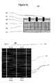
- Figure 1 shows a minimal construction for a simple solar cell.
- Solar cells are very commonly based on silicon, often in the form of a Si wafer.
- a p-n junction is commonly prepared either by providing an n-type doped Si substrate and applying a p-type doped layer to one face or by providing a p-type doped Si substrate and applying an n-type doped layer to one face to give in both cases a so called p-n junction.
- the face with the applied layer of dopant generally acts as the front face of the cell, the opposite side of the Si wafer with the original dopant acting as the back face.
- Both n-type and p-type solar cells are possible and have been exploited industrially. Cells designed to harness light incident on both faces are also possible, but their use has been less extensively harnessed.
- the front electrode In order to allow incident light on the front face of the solar cell to enter and be absorbed, the front electrode is commonly arranged in two sets of perpendicular lines known as “fingers” and “bus bars” respectively.
- the fingers form an electrical contact with the front face and bus bars link these fingers to allow charge to be drawn off effectively to the external circuit. It is common for this arrangement of fingers and bus bars to be applied in the form of an electro-conductive paste which is fired to give solid electrode bodies.
- a back electrode is also often applied in the form of an electro-conductive paste which is then fired to give a solid electrode body.
- a typical electro-conductive paste contains metallic particles, glass frit, and an organic vehicle.
- the invention is generally based on the object of overcoming at least one of the problems encountered in the state of the art in relation to solar cells, in particular in relation to those solar cells based on wafers with a high sheet resistance and those with a low dopant level on the front face, commonly referred to as high Ohmic wafers.
- the invention is further based on the object of providing solar cells with improved performance, in particular reduced contact resistance between electrodes and wafers in particular between electrodes and such high Ohmic wafers.
- a further object of the invention is to provide processes for preparing solar cells, particularly solar cells based on wafers of high Ohmic resistance and wherein the contact resistance between electrodes and wafer is reduced.
- an electro-conductive paste comprising the following paste constituents:
- the Ag-metal-oxide has the general form Ag x M y O z , wherein
- the oxidation state of M is selected from the group consisting of the following: +2, +3, +4, +5, +6, +7 preferably +5, +6 or +7.
- the Ag-metal-oxide is selected from the group consisting of the following: AgVO 3 , Ag 2 MoO 4 , Ag 2 WO 4 .
- M is selected from the group consisting of Mo, Mn, W, Cr, Nb, V, Te, Zn, Sb or at least two thereof.
- the Al metal content is less than 0.5 wt. %, preferably less than 0.1 wt. %, more preferably less than 0.01 wt. %, based on the paste. There is preferably no Al metal present in the paste.
- the Ag-metal-oxide has a melting temperature below 900 °C, preferably below about 800 °C, more preferably below about 700 °C.
- the Ag-metal-oxide is crystalline.
- a contribution to achieving at least one of the above mentioned objects is made by a precursor at least comprising as precursor parts:
- the substrate comprises at least one or more than one selected from the list consisting of the following: semiconductor, metal, or non-oxide ceramic.
- Preferred metals in this context are Fe, preferably in the form of steel; Cu; Al; Ni; Au; or Sn, preferably in the form of an alloy.
- Preferred non-oxide ceramics in this context are nitride, carbide, and boride ceramics, preferably at least one or more than one selected from the list consisting of the following: Si 3 N 4 , AlN, SiC, TiB 2 .
- the substrate is a wafer.
- the wafer has a sheet resistance of at least 80 Ohm/sq., preferably at least about 90 Ohm/sq., more preferably at least about 100 Ohm/sq..
- the paste is on the front face of the wafer.
- the paste is present on both the front face and the back face.
- the paste is on a p-type doped face of the wafer.
- the paste is on an n-type doped face of the wafer.
- a contribution to achieving at least one of the above mentioned objects is made by a process for the preparation of a device at least comprising the steps:
- the device is a photovoltaic solar cell.
- the paste is transformed into an electrode which is attached to the substrate.
- the substrate and the electrode often form a composite.
- the maximum temperature during the firing step is less than about 900 °C, preferably less than about 870 °C, more preferably less than about 850 °C.
- a contribution to achieving at least one of the above mentioned objects is made by a solar cell obtainable by the process according to the invention.
- module comprising at least one solar cell according to the invention and at least a further solar cell.
- Preferred substrates are materials which comprise at least one or more than one selected from the list consisting of the following: semiconductor, metal, or non-oxide ceramic.
- Preferred metals in this context are Fe, preferably in the form of steel; Cu; Al; Ni; Au; or Sn, preferably in the form of an alloy.
- Preferred non-oxide ceramics in this context are nitride, carbide, and boride ceramics, preferably at least one or more than one selected from the list consisting of the following: Si 3 N 4 , AlN, SiC, TiB 2 .
- Preferred substrates are wafers.
- Preferred wafers according to the invention are regions among other regions of the solar cell capable of absorbing light with high efficiency to yield electron-hole pairs and separating holes and electrons across a boundary with high efficiency, preferably across a so called p-n junction boundary.
- Preferred wafers according to the invention are those comprising a single body made up of a front doped layer and a back doped layer.
- wafer consist of appropriately doped tetravalent elements, binary compounds, tertiary compounds or alloys.
- Preferred tetravalent elements in this context are Si, Ge or Sn, preferably Si.
- Preferred binary compounds are combinations of two or more tetravalent elements, binary compounds of a group III element with a group V element, binary compounds of a group II element with a group VI element or binary compounds of a group IV element with a group VI element.
- Preferred combinations of tetravalent elements are combinations of two or more elements selected from Si, Ge, Sn or C, preferably SiC.
- the preferred binary compounds of a group III element with a group V element is GaAs. It is most preferred according to the invention for the wafer to be based on Si. Si, as the most preferred material for the wafer, is referred to explicitly throughout the rest of this application. Sections of the following text in which Si is explicitly mentioned also apply for the other wafer compositions described above.
- the front doped layer and back doped layer of the wafer meet is the p-n junction boundary.
- the back doped layer is doped with electron donating n-type dopant and the front doped layer is doped with electron accepting or hole donating p-type dopant.
- the back doped layer is doped with p-type dopant and the front doped layer is doped with n-type dopant. It is preferred according to the invention to prepare a wafer with a p-n junction boundary by first providing a doped Si substrate and then applying a doped layer of the opposite type to one face of that substrate.
- Doped Si substrates are well known to the person skilled in the art.
- the doped Si substrate can be prepared in any way known to the person skilled in the art and which he considers to be suitable in the context of the invention.
- Preferred sources of Si substrates according to the invention are mono-crystalline Si, multi-crystalline Si, amorphous Si and upgraded metallurgical Si, mono-crystalline Si or multi-crystalline Si being most preferred.
- Doping to form the doped Si substrate can be carried out simultaneously by adding dopant during the preparation of the Si substrate or can be carried out in a subsequent step. Doping subsequent to the preparation of the Si substrate can be carried out for example by gas diffusion epitaxy.
- Doped Si substrates are also readily commercially available.
- the initial doping of the Si substrate it is one option for the initial doping of the Si substrate to be carried out simultaneously to its formation by adding dopant to the Si mix.
- This gas phase epitaxy is preferably carried out at a temperature in a range from 500 °C to 900 °C, more preferably in a range from 600 °C to 800 °C and most preferably in a range from 650 °C to 750 °C at a pressure in a range from 2 kPa and 100 kPa, preferably in a range from 10 to 80 kPa, most preferably in a range from 30 to 70 kPa.
- Si substrates can exhibit a number of shapes, surface textures and sizes.
- the shape can be one of a number of different shapes including cuboid, disc, wafer and irregular polyhedron amongst others.
- the preferred shape according to the invention is wafer shaped where that wafer is a cuboid with two dimensions which are similar, preferably equal and a third dimension which is significantly less than the other two dimensions. Significantly less in this context is preferably at least a factor of 100 smaller.
- Si substrates with rough surfaces are preferred.
- One way to assess the roughness of the substrate is to evaluate the surface roughness parameter for a sub-surface of the substrate which is small in comparison to the total surface area of the substrate, preferably less than one hundredth of the total surface area, and which is essentially planar.
- the value of the surface roughness parameter is given by the ratio of the area of the subsurface to the area of a theoretical surface formed by projecting that subsurface onto the flat plane best fitted to the subsurface by minimizing mean square displacement.
- a higher value of the surface roughness parameter indicates a rougher, more irregular surface and a lower value of the surface roughness parameter indicates a smoother, more even surface.
- the surface roughness of the Si substrate is preferably modified so as to produce an optimum balance between a number of factors including but not limited to light absorption and adhesion of fingers to the surface.
- the two dimensions with larger scale of the Si substrate can be varied to suit the application required of the resultant solar cell. It is preferred according to the invention for the thickness of the Si wafer to lie below 0.5 mm more preferably below 0.3 mm and most preferably below 0.2 mm. Some wafers have a minimum size of 0.01 mm or more.
- the front doped layer is thin in comparison to the back doped layer. It is preferred according to the invention for the front doped layer to have a thickness lying in a range from 0.1 to 10 ⁇ m, preferably in a range from 0.1 to 5 ⁇ m and most preferably in a range from 0.1 to 2 ⁇ m.
- a highly doped layer can be applied to the back face of the Si substrate between the back doped layer and any further layers.
- Such a highly doped layer is of the same doping type as the back doped layer and such a layer is commonly denoted with a + (n + -type layers are applied to n-type back doped layers and p + -type layers are applied to p-type back doped layers).
- This highly doped back layer serves to assist metallisation and improve electro-conductive properties at the substrate/electrode interface area.
- the highly doped back layer if present, to have a thickness in a range from 1 to 100 ⁇ m, preferably in a range from 1 to 50 ⁇ m and most preferably in a range from 1 to 15 ⁇ m.
- Preferred dopants are those which, when added to the Si wafer, form a p-n junction boundary by introducing electrons or holes into the band structure. It is preferred according to the invention that the identity and concentration of these dopants is specifically selected so as to tune the band structure profile of the p-n junction and set the light absorption and conductivity profiles as required.
- Preferred p-type dopants according to the invention are those which add holes to the Si wafer band structure. They are well known to the person skilled in the art. All dopants known to the person skilled in the art and which he considers to be suitable in the context of the invention can be employed as p-type dopant.
- Preferred p-type dopants according to the invention are trivalent elements, particularly those of group 13 of the periodic table. Preferred group 13 elements of the periodic table in this context include but are not limited to B, Al, Ga, In, TI or a combination of at least two thereof, wherein B is particularly preferred.
- Preferred n-type dopants according to the invention are those which add electrons to the Si wafer band structure. They are well known to the person skilled in the art. All dopants known to the person skilled in the art and which he considers to be suitable in the context of the invention can be employed as n-type dopant.
- Preferred n-type dopants according to the invention are elements of group 15 of the periodic table. Preferred group 15 elements of the periodic table in this context include N, P, As, Sb, Bi or a combination of at least two thereof, wherein P is particularly preferred.
- the various doping levels of the p-n junction can be varied so as to tune the desired properties of the resulting solar cell. It is preferred according to the invention for the wafer to have a sheet resistance of at least 80 Ohm/sq., more preferably at least 90 Ohm/sq. and most preferably at least 100 Ohm/sq. In some cases, a maximum value of 200 Ohm/sq. is observed for the sheet resistance of high Ohmic wafers.
- the back doped layer is lightly doped, preferably with a dopant concentration in a range from 1 x 10 13 to 1 x 10 18 cm -3 , preferably in a range from 1 x 10 14 to 1 x 10 17 cm -3 , most preferably in a range from 5 x 10 15 to 5 x 10 16 cm -3 .
- Some commercial products have a back doped layer with a dopant concentration of about 1 x 10 16 .
- the highly doped back layer (if one is present) to be highly doped, preferably with a concentration in a range from 1 x 10 17 to 5 x 10 21 cm -3 , more preferably in a range from 5 x 10 17 to 5 x 10 20 cm -3 , and most preferably in a range from 1 x 10 18 to 1 x 10 19 cm -3 .
- Preferred electro-conductive pastes according to the invention are pastes which can be applied to a surface and which, on firing, form solid electrode bodies in electrical contact with that surface.
- Preferred electro-conductive pastes in the context of the invention are those which comprise as paste components:
- the viscosity of the electro-conductive paste lie in a range from 10-30 Pa*s, preferably in a range from 12-25 Pa*s and most preferably in a range from 15-22 Pa*s.
- the electro-conductive paste is on the front face of the wafer. In further embodiments, the electro conductive paste is on the back face of the wafer or even on both faces and/or in a hole penetrating the wafer. Such holes are often called via holes and are commonly used in so called metal wrap through designs which are described in WO 2012/026812 A1 and WO 2012/026806 A1 .
- Ag-metal-oxides in the context of the invention are compounds which comprise silver, oxygen and a metal or semi-metal element other than silver.
- Ag-metal-oxides are known to the skilled person and he may select an Ag-metal-oxide which he considers suitable in the context of the invention in order to enhance favourable properties of the solar cell, preferably a reduced specific contact resistance between electrodes and wafer.
- the Ag-metal-oxide is a binary oxide with the general formula Ag x M y O z , wherein M stands for a metal or semi-metal element other than Ag and x, y and z are positive integers which may take on different values depending on M.
- M stands for a metal or semi-metal element other than Ag
- y and z are positive integers which may take on different values depending on M.
- x is an integer in the range from 1 to 5, preferably 1 or 2
- y is 1
- z is an integer in the range from 1 to 6, preferably 3 or 4.
- the Ag-metal-oxide contains at least two or more metals or semi-metal elements other than Ag.
- the metal or metals other than Ag may be selected by the skilled person in order to bring about favourable characteristics of the solar cell, preferably reduced specific contact resistance between electrode and wafer.
- the skilled person may also vary the stoichiometry, oxidation states, phase properties, crystal structures and other physical properties as he sees fit.
- At least metal other than Ag in the Ag-metal-oxide has two or more common oxidation states.
- At least one of the metals other than Ag is in an oxidation states selected from the list consisting of the following: +3, +4, +5, +6, preferably +5 or +6.
- At least metal other than Ag in the Ag-metal-oxide is a transition metal.
- Preferred metals or semi-metal elements in this context are one or more selected from the group consisting of the following: Sn, Pb, Se, As, Bi, Mo, Mn, W, Cr, Nb, V, Te, Zn, Sb, Si; more preferably from the group consisting of the following: Mo, Mn, W, Cr, Nb, V, Te, Zn, Sb; most preferably from the group consisting of the following: V, W, Mo.
- Preferred metals in this context are one or more selected from the group consisting of the following: Sn, Pb, Se, As, Bi, Mo, Mn, W, Cr, Nb, V, Te, Zn, Sb,; more preferably from the group consisting of the following: Mo, Mn, W, Cr, Nb, V, Te, Zn, Sb; most preferably from the group consisting of the following: V, W, Mo.
- the Ag-metal-oxide is preferably at least one or more selected from the group consisting of the following: AgV 7 O 18 , Ag 2 V 4 O 11 , AgVO 3 , Ag 4 V 2 O 7 , Ag 2 MO 4 O 13. Ag 2 Mo 2 O 7.
- the Ag-metal-oxide is more preferably at least one or more selected from the group consisting of the following: AgVO 3 , Ag 4 V 2 O 7 , AgCrO 2 Ag 2 MoO 4 , AgVMoO 6 Ag 2 WO 4 , Ag 2 SeO 4 , Ag 2 TeO 4 , Ag 2 TeO 3 , Ag 2 Te 4 O 11 , AgSbO 3 , AgNbO 3 , Ag 2 SiO 3 , Ag 4 SiO 4 , Ag 2 Si 2 O 5 .
- the Ag-metal-oxide is most preferably at least one or more selected from the group consisting of the following: AgVO 3 , Ag 2 MoO 4 , Ag 2 WO 4 .
- Ag-metal-oxide comprising semi-metals is preferably at least one or more selected from the group consisting of the following: Te, Sb, SI.
- the Ag-metal-oxide comprising M as a semi-metals is most preferably at least one or more selected from the group consisting of the following: Ag 2 TeO 3 , AgSbO 3 , Ag 4 SiO 4 .
- the Ag-metal-oxide be molten at the firing temperature.
- the Ag-metal-oxide has a melting point below about 900 °C, preferably below about 800 °C, more preferably below about 700 °C.
- the Ag-metal-oxide is preferably present in the electro-conductive paste in a concentration in a range from about 2 to about 50 mmol/kg more preferably in a range from about 5 to about 30 mmol/kg, and most preferably in a range from about 10 to about 25 mmol/kg, in each case based on the amount of Ag + ions in the Ag-metal-oxide and the total weight of the Ag-metal-oxide.
- the skilled person may choose the specific crystal structure for the Ag-metal-oxide in order to improve the favourable properties of the solar cell.
- Preferred crystal types are hexagonal, or-thorhombic, rhombohedral, triclinic, cubic, tetragonal and monoclinic.
- Preferred metallic particles in the context of the invention are those which exhibit metallic conductivity or which yield a substance which exhibits metallic conductivity on firing.
- Metallic particles present in the electro-conductive paste gives metallic conductivity to the solid electrode which is formed when the electro-conductive paste is sintered on firing.
- Metallic particles which favour effective sintering and yield electrodes with high conductivity and low contact resistance are preferred.
- Metallic particles are well known to the person skilled in the art. All metallic particles known to the person skilled in the art and which he considers suitable in the context of the invention can be employed as the metallic particles in the electro-conductive paste.
- Preferred metallic particles according to the invention are metals, alloys, mixtures of at least two metals, mixtures of at least two alloys or mixtures of at least one metal with at least one alloy.
- Preferred metals which can be employed as metallic particles according to the invention are Ag, Au, Pt, Cu, Al, Zn, Pd, Ni or Pb and mixtures of at least two thereof, preferably Ag.
- Preferred alloys which can be employed as metallic particles according to the invention are alloys containing at least one metal selected from the list of Ag, Au, Pt, Cu, Al, Zn, Ni, W, Pb and Pd or mixtures or two or more of those alloys.
- the metallic particles comprise a metal or alloys coated with one or more further different metals or alloys, for example copper coated with silver.
- the metallic particles comprise Ag. In another embodiment according to the invention, the metallic particles comprise a mixture of Ag with Al.
- the Al content of the paste be low, preferably less than 0.1 wt. %, more preferably less than 0.01 wt. %, preferably zero.
- the paste is applied to a p-type doped surface and optionally also an n-type doped surface.
- n-type dopants are group 15 elements or compounds which yield such elements on firing.
- Preferred group 15 elements in this context according to the invention are P and Bi.
- additives capable of acting as p-type dopants in Si are preferred.
- Preferred p-type dopants are group 13 elements or compounds which yield such elements on firing.
- Preferred group 13 elements in this context according to the invention are B and Al.
- metallic particles can exhibit a variety of shapes, surfaces, sizes, surface area to volume ratios, oxygen content and oxide layers.
- a large number of shapes are known to the person skilled in the art. Some examples are spherical, angular, elongated (rod or needle like) and flat (sheet like).
- Metallic particles may also be present as a combination of particles of different shapes. Metallic particles with a shape, or combination of shapes, which favours advantageous sintering, electrical contact, adhesion and electrical conductivity of the produced electrode are preferred according to the invention.
- One way to characterise such shapes without considering surface nature is through the parameters length, width and thickness.
- the length of a particle is given by the length of the longest spatial displacement vector, both endpoints of which are contained within the particle.
- the width of a particle is given by the length of the longest spatial displacement vector perpendicular to the length vector defined above both endpoints of which are contained within the particle.
- the thickness of a particle is given by the length of the longest spatial displacement vector perpendicular to both the length vector and the width vector, both defined above, both endpoints of which are contained within the particle.
- metallic particles with shapes as uniform as possible are preferred i.e.
- the ratios relating the length, the width and the thickness are as close as possible to 1, preferably all ratios lying in a range from 0.7 to 1.5, more preferably in a range from 0.8 to 1.3 and most preferably in a range from 0.9 to 1.2.
- preferred shapes for the metallic particles in this embodiment are therefore spheres and cubes, or combinations thereof, or combinations of one or more thereof with other shapes.
- metallic particles are preferred which have a shape of low uniformity, preferably with at least one of the ratios relating the dimensions of length, width and thickness being above 1.5, more preferably above 3 and most preferably above 5.
- Preferred shapes according to this embodiment are flake shaped, rod or needle shaped, or a combination of flake shaped, rod or needle shaped with other shapes.
- metallic particles with a high surface area to volume ratio are preferred, preferably in a range from 1.0 ⁇ 10 7 to 1.0 ⁇ 10 9 m -1 , more preferably in a range from 5.0 ⁇ 10 7 to 5.0 ⁇ 10 8 m -1 and most preferably in a range from 1.0 ⁇ 10 8 to 5.0 ⁇ 10 8 m -1 .
- metallic particles with a low surface area to volume ratio are preferred, preferably in a range from 6 ⁇ 10 5 to 8.0 ⁇ 10 6 m -1 , more preferably in a range from 1.0 ⁇ 10 6 to 6.0 ⁇ 10 6 m -1 and most preferably in a range from 2.0 ⁇ 10 6 to 4.0 ⁇ 10 6 m -1 .
- the particles diameter d 50 and the associated values d 10 and d 90 are characteristics of particles well known to the person skilled in the art. It is preferred according to the invention that the average particle diameter d 50 of the metallic particles lie in a range from 0.5 to 10 ⁇ m, more preferably in a range from 1 to 10 ⁇ m and most preferably in a range from 1 to 5 ⁇ m. The determination of the particles diameter d 50 is well known to a person skilled in the art..
- the metallic particles may be present with a surface coating. Any such coating known to the person skilled in the art and which he considers to be suitable in the context of the invention can be employed on the metallic particles.
- Preferred coatings according to the invention are those coatings which promote improved printing, sintering and etching characteristics of the electro-conductive paste. If such a coating is present, it is preferred according to the invention for that coating to correspond to no more than 10 wt. %, preferably no more than 8 wt. %, most preferably no more than 5 wt. %, in each case based on the total weight of the metallic particles.
- the metallic particles are present as a proportion of the electro-conductive paste more than 50 wt. %, preferably more than 70 wt. %, most preferably more than 80 wt. %.
- Preferred glass frits in the context of the invention are powders of amorphous or partially crystalline solids which exhibit a glass transition.
- the glass transition temperature T g is the temperature where an amorphous substance transfers from a rigid solid to a partially mobile undercooled melt upon heating. Methods for the determination of the glass transition temperature are well known to the person skilled in the art.
- Glass frit is present in the electro-conductive paste according to the invention in order to bring about etching and sintering. Effective etching is required to etch through any additional layers which may have been applied to the Si wafer and thus lie between the front doped layer and the applied electro-conductive paste as well as to etch into the Si wafer to an appropriate extent.
- etching of the Si wafer means deep enough to bring about good electrical contact between the electrode and the front doped layer and thus lead to a low contact resistance but not as deep as to interfere with the p-n junction boundary.
- the etching and sintering brought about by the glass frit occurs above the glass transition temperature of the glass frit and the glass transition temperature must lie below the desired peak firing temperature.
- Glass frits are well known to the person skilled in the art. All glass frits known to the person skilled in the art and which he considers suitable in the context of the invention can be employed as the glass frit in the electro-conductive paste.
- the glass frit must have a glass transition temperature below the desired firing temperature of the electro-conductive paste.
- preferred glass frits have a glass transition temperature in the range 250 °C to 700 °C, preferably in the range 300 °C to 600 °C and most preferably in the range 350 °C to 500 °C.
- glass frit particles can exhibit a variety of shapes, surface natures, sizes, surface area to volume ratios and coating layers.
- a large number of shapes of glass frit particles are known to the person skilled in the art. Some examples are spherical, angular, elongated (rod or needle like) and flat (sheet like).
- Glass frit particles may also be present as a combination of particles of different shapes. Glass frit particles with a shape, or combination of shapes, which favours advantageous sintering, adhesion, electrical contact and electrical conductivity of the produced electrode are preferred according to the invention.
- a way to characterise the shape and surface of a particle is by its surface area to volume ratio.
- the lowest value for the surface area to volume ratio of a particle is embodied by a sphere with a smooth surface. The less uniform and uneven a shape is, the higher its surface area to volume ratio will be.
- glass frit particles with a high surface area to volume ratio are preferred, preferably in a range from 1.0 ⁇ 10 7 to 1.0 ⁇ 10 9 m -1 , more preferably in a range from 5.0 ⁇ 10 7 to 5.0 ⁇ 10 8 m -1 and most preferably in a range from 1.0 ⁇ 10 8 to 5.0 ⁇ 10 8 m -1 .
- glass frit particles with a low surface area to volume ratio are preferred, preferably in a range from 6 ⁇ 10 5 to 8.0 ⁇ 10 6 m -1 , more preferably in a range from 1.0 ⁇ 10 6 to 6.0 ⁇ 10 6 m -1 and most preferably in a range from 2.0 ⁇ 10 6 to 4.0 ⁇ 10 6 m -1 .
- the average particles diameter d 50 , and the associated parameters d 10 and d 90 are characteristics of particles well known to the person skilled in the art. It is preferred according to the invention that the average particle diameter d 50 of the glass frit lie in a range from 0.5 to 10 ⁇ m, more preferably in a range from 1 to 7 ⁇ m and most preferably in a range from 1 to 5 ⁇ m. The determination of the particles diameter d 50 is well known to a person skilled in the art.
- the glass frit particles may be present with a surface coating. Any such coating known to the person skilled in the art and which he considers to be suitable in the context of the invention can be employed on the glass frit particles.
- Preferred coatings according to the invention are those coatings which promote improved printing, sintering and etching characteristics of the electro-conductive paste. If such a coating is present, it is preferred according to the invention for that coating to correspond to no more than 10 wt. %, preferably no more than 8 wt. %, most preferably no more than 5 wt. %, in each case based on the total weight of the glass frit particles.
- Preferred organic vehicles in the context of the invention are solutions, emulsions or dispersions based on a one or more solvents, preferably an organic solvent, which ensure that the constituents of the electro-conductive paste are present in a dissolved, emulsified or dispersed form.
- Preferred organic vehicles are those which provide optimal stability of constituents with-in the electro-conductive paste and endow the electro-conductive paste with a viscosity allowing effective line printability.
- Preferred organic vehicles according to the invention comprise as vehicle components:
- Preferred binders in the context of the invention are those which contribute to the formation of an electro-conductive paste with favourable stability, printability, viscosity, sintering and etching properties. Binders are well known to the person skilled in the art. All binders which are known to the person skilled in the art and which he considers to be suitable in the context of this invention can be employed as the binder in the organic vehicle. Preferred binders according to the invention (which often fall within the category termed "resins”) are polymeric binders, monomeric binders, and binders which are a combination of polymers and monomers. Polymeric binders can also be copolymers where at least two different monomeric units are contained in a single molecule.
- Preferred polymeric binders are those which carry functional groups in the polymer main chain, those which carry functional groups off of the main chain and those which carry functional groups both within the main chain and off of the main chain.
- Preferred polymers carrying functional groups in the main chain are for example polyesters, substituted polyesters, polycarbonates, substituted polycarbonates, polymers which carry cyclic groups in the main chain, poly-sugars, substituted poly-sugars, polyurethanes, substituted polyurethanes, polyamides, substituted polyamides, phenolic resins, substituted phenolic resins, copolymers of the monomers of one or more of the preceding polymers, optionally with other co-monomers, or a combination of at least two thereof.
- Preferred polymers which carry cyclic groups in the main chain are for example polyvinylbutylate (PVB) and its derivatives and poly-terpineol and its derivatives or mixtures thereof.
- Preferred poly-sugars are for example cellulose and alkyl derivatives thereof, preferably methyl cellulose, ethyl cellulose, propyl cellulose, butyl cellulose and their derivatives and mixtures of at least two thereof.
- Other preferred polymers are cellulose ester resins e.g. selected from the group consisting of cellulose acetate propionate, cellulose acetate butyrate, and mixtures thereof, preferably those disclosed in US 2013 180583 which is herewith incorporated by reference.
- Preferred polymers which carry functional groups off of the main polymer chain are those which carry amide groups, those which carry acid and/or ester groups, often called acrylic resins, or polymers which carry a combination of aforementioned functional groups, or a combination thereof.
- Preferred polymers which carry amide off of the main chain are for example polyvinyl pyrrolidone (PVP) and its derivatives.
- Preferred polymers which carry acid and/or ester groups off of the main chain are for example polyacrylic acid and its derivatives, polymethacrylate (PMA) and its derivatives or polymethylmethacrylate (PMMA) and its derivatives, or a mixture thereof.
- Preferred monomeric binders according to the invention are ethylene glycol based monomers, terpineol resins or rosin derivatives, or a mixture thereof.
- Preferred monomeric binders based on ethylene glycol are those with ether groups, ester groups or those with an ether group and an ester group, preferred ether groups being methyl, ethyl, propyl, butyl, pentyl hexyl and higher alkyl ethers, the preferred ester group being acetate and its alkyl derivatives, preferably ethylene glycol monobutylether monoacetate or a mixture thereof.
- Alkyl cellulose, preferably ethyl cellulose, its derivatives and mixtures thereof with other binders from the preceding lists of binders or otherwise are the most preferred binders in the context of the invention.
- Preferred surfactants in the context of the invention are those which contribute to the formation of an electro-conductive paste with favourable stability, printability, viscosity, sintering and etching properties.
- Surfactants are well known to the person skilled in the art. All surfactants which are known to the person skilled in the art and which he considers to be suitable in the context of this invention can be employed as the surfactant in the organic vehicle.
- Preferred surfactants in the context of the invention are those based on linear chains, branched chains, aromatic chains, fluorinated chains, siloxane chains, polyether chains and combinations thereof. Preferred surfactants are single chained double chained or poly chained.
- Preferred surfactants according to the invention have non-ionic, anionic, cationic, or zwitterionic heads.
- Preferred surfactants are polymeric and monomeric or a mixture thereof.
- Preferred surfactants according to the invention can have pigment affinic groups, preferably hydroxyfunctional carboxylic acid esters with pigment affinic groups (e.g., DISPERBYK ® -108, manufactured by BYK USA, Inc.), acrylate copolymers with pigment affinic groups (e.g., DISPERBYK ® -116, manufactured by BYK USA, Inc.), modified polyethers with pigment affinic groups (e.g., TEGO ® DISPERS 655, manufactured by Evonik Tego Chemie GmbH), other surfactants with groups of high pigment affinity (e.g., TEGO ® DISPERS 662 C, manufactured by Evonik Tego Chemie GmbH).
- pigment affinic groups preferably hydroxyfunctional carboxylic acid esters with pigment
- polyethyleneglycol and its derivatives are polyethyleneglycol and its derivatives, and alkyl carboxylic acids and their derivatives or salts, or mixtures thereof.
- the preferred polyethyleneglycol derivative according to the invention is poly(ethyleneglycol)acetic acid.
- Preferred alkyl carboxylic acids are those with fully saturated and those with singly or poly unsaturated alkyl chains or mixtures thereof.
- Preferred carboxylic acids with saturated alkyl chains are those with alkyl chains lengths in a range from 8 to 20 carbon atoms, preferably C 9 H 19 COOH (capric acid), C 11 H 23 COOH (Lauric acid), C 13 H 27 COOH (myristic acid) C 15 H 31 COOH (palmitic acid), C 17 H 35 COOH (stearic acid) or mixtures thereof.
- Preferred carboxylic acids with unsaturated alkyl chains are C 18 H 34 O 2 (oleic acid) and C 18 H 32 O 2 (linoleic acid).
- the preferred monomeric surfactant according to the invention is benzotriazole and its derivatives.
- Preferred solvents according to the invention are constituents of the electro-conductive paste which are removed from the paste to a significant extent during firing, preferably those which are present after firing with an absolute weight reduced by at least 80% compared to before firing, preferably reduced by at least 95% compared to before firing.
- Preferred solvents according to the invention are those which allow an electro-conductive paste to be formed which has favourable viscosity, printability, stability and sintering characteristics and which yields electrodes with favourable electrical conductivity and electrical contact to the substrate. Solvents are well known to the person skilled in the art. All solvents which are known to the person skilled in the art and which he considers to be suitable in the context of this invention can be employed as the solvent in the organic vehicle.
- preferred solvents are those which allow the preferred high level of printability of the electro-conductive paste as described above to be achieved.
- Preferred solvents according to the invention are those which exist as a liquid under standard ambient temperature and pressure (SATP) (298.15 K, 25 °C, 77 °F), 100 kPa (14.504 psi, 0.986 atm), preferably those with a boiling point above 90 °C and a melting point above -20 °C.
- Preferred solvents according to the invention are polar or nonpolar, protic or aprotic, aromatic or non-aromatic.
- Preferred solvents according to the invention are mono-alcohols, di-alcohols, poly-alcohols, mono-esters, di-esters, poly-esters, monoethers, di-ethers, poly-ethers, solvents which comprise at least one or more of these categories of functional group, optionally comprising other categories of functional group, preferably cyclic groups, aromatic groups, unsaturated-bonds, alcohol groups with one or more O atoms replaced by heteroatoms, ether groups with one or more O atoms replaced by heteroatoms, esters groups with one or more O atoms replaced by heteroatoms, and mixtures of two or more of the aforementioned solvents.
- Preferred esters in this context are di-alkyl esters of adipic acid, preferred alkyl constituents being methyl, ethyl, propyl, butyl, pentyl, hexyl and higher alkyl groups or combinations of two different such alkyl groups, preferably dimethyladipate, and mixtures of two or more adipate esters.
- Preferred ethers in this context are diethers, preferably dialkyl ethers of ethylene glycol, preferred alkyl constituents being methyl, ethyl, propyl, butyl, pentyl, hexyl and higher alkyl groups or combinations of two different such alkyl groups, and mixtures of two diethers.
- Preferred alcohols in this context are primary, secondary and tertiary alcohols, preferably tertiary alcohols, terpineol and its derivatives being preferred, or a mixture of two or more alcohols.
- Preferred solvents which combine more than one different functional groups are 2,2,4-trimethyl-1,3-pentanediol monoisobutyrate, often called texanol, and its derivatives, 2-(2-ethoxyethoxy)ethanol, often known as carbitol, its alkyl derivatives, preferably methyl, ethyl, propyl, butyl, pentyl, and hexyl carbitol, preferably hexyl carbitol or butyl carbitol, and acetate derivatives thereof, preferably butyl carbitol acetate, or mixtures of at least 2 of the aforementioned.
- Preferred additives in the organic vehicle are those additives which are distinct from the aforementioned vehicle components and which contribute to favourable properties of the electro-conductive paste, such as advantageous viscosity, sintering, electrical conductivity of the produced electrode and good electrical contact with substrates. All additives known to the person skilled in the art and which he considers to be suitable in the context of the invention can be employed as additive in the organic vehicle.
- Preferred additives according to the invention are thixotropic agents, viscosity regulators, stabilising agents, inorganic additives, thickeners, emulsifiers, dispersants or pH regulators.
- Preferred thixotropic agents in this context are carboxylic acid derivatives, preferably fatty acid derivatives or combinations thereof.
- Preferred fatty acid derivatives are C 9 H 19 COOH (capric acid), C 11 H 23 COOH (Lauric acid), C 13 H 27 COOH (myristic acid) C 15 H 31 COOH (palmitic acid), C 17 H 35 COOH (stearic acid) C 18 H 34 O 2 (oleic acid), C 18 H 32 O 2 (linoleic acid) or combinations thereof.
- a preferred combination comprising fatty acids in this context is castor oil.
- Preferred additives in the context of the invention are constituents added to the electro-conductive paste, in addition to the other constituents explicitly mentioned, which contribute to increased performance of the electro-conductive paste, of the electrodes produced thereof or of the resulting solar cell. All additives known to the person skilled in the art and which he considers suitable in the context of the invention can be employed as additive in the electro-conductive paste. In addition to additives present in the vehicle, additives can also be present in the electro-conductive paste. Preferred additives according to the invention are thixotropic agents, viscosity regulators, emulsifiers, stabilising agents or pH regulators, inorganic additives, thickeners and dispersants or a combination of at least two thereof, whereas inorganic additives are most preferred.
- a contribution to achieving at one of the aforementioned objects is made by a process for producing a solar cell at least comprising the following as process steps:
- the front and back electrodes are applied by applying an electro-conductive paste and then firing said electro-conductive paste to obtain a sintered body.
- the electro-conductive paste can be applied in any manner known to the person skilled in that art and which he considers suitable in the context of the invention including but not limited to impregnation, dipping, pouring, dripping on, injection, spraying, knife coating, curtain coating, brushing or printing or a combination of at least two thereof, wherein preferred printing techniques are ink-jet printing, screen printing, tampon printing, offset printing, relief printing or stencil printing or a combination of at least two thereof.
- the electro-conductive paste is applied by printing, preferably by screen printing. It is preferred according to the invention that the screens have mesh opening with a diameter in a range from 20 to 100 ⁇ m, more preferably in a range from 30 to 80 ⁇ m, and most preferably in a range from 40 to 70 ⁇ m.
- electrodes prefferably formed by first applying an electro-conductive paste and then firing said electro-conductive paste to yield a solid electrode body. Firing is well known to the person skilled in the art and can be effected in any manner known to him and which he considers suitable in the context of the invention. Firing must be carried out above the glass transition temperature of the glass frit.
- the maximum temperature set for the firing is below 900 °C, preferably below 860 °C. Firing temperatures as low as 820 °C have been employed for obtaining solar cells. It is preferred according to the invention for firing to be carried out in a fast firing process with a total firing time in the range from 30 s to 3 minutes, more preferably in the range from 30 s to 2 minutes and most preferably in the range from 40 s to 1 minute. The time above 600 °C is most preferably from 3 to 7 s.
- Firing of electro-conductive pastes on the front and back faces can be carried out simultaneously or sequentially. Simultaneous firing is appropriate if the electro-conductive pastes applied to both faces have similar, preferably identical, optimum firing conditions. Where appropriate, it is preferred according to the invention for firing to be carried out simultaneously. Where firing is affected sequentially, it is preferable according to the invention for the back electro-conductive paste to be applied and fired first, followed by application and firing of the electro-conductive paste to the front face.
- a contribution to achieving at least one of the above described objects is made by a solar cell obtainable by a process according to the invention.
- Preferred solar cells according to the invention are those which have a high efficiency in terms of proportion of total energy of incident light converted into electrical energy output and which are light and durable.
- the common configuration of a solar cell according to the invention (excluding layers which are purely for chemical and mechanical protection) is as depicted in figure 2 .
- the layer configuration shown there is given as follows: (i) Front electrode, (ii) Anti reflection coating, (iii) Front passivation layer, (iv) Front doped layer, (v) p-n junction boundary, (vi) Back doped layer, (vii) Highly doped back layer, (viii) Back passivation layer, (ix) Back electrode.
- a single layer acts as both anti-reflection layer and passivation layer.
- the minimum required layer configuration is given in figure 1 . This minimum layer configuration is as follows: (I) Front electrode, (II) Front doped layer, (III) p-n junction boundary, (IV) Back doped layer, (V) Back electrode.
- the wafer comprises both a p-type doped region and an n-type doped region which are both present on the same face of the wafer.
- the inventive paste is applied to both the p-type doped region and the n-type doped region which are present on the same face.
- This type of cell is commonly referred to as an Interdigitated Back Contact (IBC) cell. Further information on IBC cells can be found in the following and they are hereby incorporated as part of this application: W. P. Mulligan, D. H. Rose, M. J.
- the solar cell comprises a wafer with a sheet resistance of at least 80 Ohm/sq., preferably at least 90 Ohm/sq. more preferably at least 100 Ohm/sq. In some cases, a maximum value of 200 Ohm/sq. is observed for the sheet resistance of high Ohmic wafers.
- both front and back face electrodes are produced using a paste according to the invention.
- an anti-reflection coating can be applied as the outer and often as the outermost layer before the electrode on the front face of the solar cell.
- Preferred anti-reflection coatings according to the invention are those which decrease the proportion of incident light reflected by the front face and increase the proportion of incident light crossing the front face to be absorbed by the wafer.
- Anti-reflection coatings which give rise to a favourable absorption/reflection ratio are susceptible to etching by the employed electro-conductive paste but are otherwise resistant to the temperatures required for firing of the electro-conductive paste, and do not contribute to increased recombination of electrons and holes in the vicinity of the electrode interface are favoured.
- anti-reflection coatings known to the person skilled in the art and which he considers to be suitable in the context of the invention can be employed.
- Preferred anti-reflection coatings according to the invention are SiN x , SiO 2 , Al 2 O 3 , TiO 2 or mixtures of at least two thereof and/or combinations of at least two layers thereof, wherein SiN x is particularly preferred, in particular where an Si wafer is employed.
- anti-reflection coatings is suited to the wavelength of the appropriate light. According to the invention it is preferred for anti-reflection coatings to have a thickness in a range from 20 to 300 nm, more preferably in a range from 40 to 200 nm and most preferably in a range from 60 to 90 nm.
- one or more passivation layers can be applied to the front and/or back side as outer or as the outermost layer before the electrode, or before the anti-reflection layer if one is present.
- Preferred passivation layers are those which reduce the rate of electron/hole recombination in the vicinity of the electrode interface. Any passivation layer which is known to the person skilled in the art and which he considers to be suitable in the context of the invention can be employed.
- Preferred passivation layers according to the invention are silicon nitride, silicon dioxide and titanium dioxide, silicon nitride being most preferred.
- the passivation layer it is preferred for the passivation layer to have a thickness in a range from 0.1 nm to 2 ⁇ m, more preferably in a range from 10 nm to 1 ⁇ m and most preferably in a range from 30 nm to 200 nm.
- the cell can be encapsulated to provide chemical protection. Encapsulations are well known to the person skilled in the art and any encapsulation can be employed which is known to him and which he considers suitable in the context of the invention.
- transparent polymers often referred to as transparent thermoplastic resins, are preferred as the encapsulation material, if such an encapsulation is present.
- Preferred transparent polymers in this context are for example silicon rubber and polyethylene vinyl acetate (PVA).
- a transparent glass sheet can be added to the front of the solar cell to provide mechanical protection to the front face of the cell.
- Transparent glass sheets are well known to the person skilled in the art and any transparent glass sheet known to him and which he considers to be suitable in the context of the invention can be employed as protection on the front face of the solar cell.
- a back protecting material can be added to the back face of the solar cell to provide mechanical protection.
- Back protecting materials are well known to the person skilled in the art and any back protecting material which is known to the person skilled in the art and which he considers to be suitable in the context of the invention can be employed as protection on the back face of the solar cell.
- Preferred back protecting materials according to the invention are those having good mechanical properties and weather resistance.
- the preferred back protection materials according to the invention is polyethylene terephthalate with a layer of polyvinyl fluoride. It is preferred according to the invention for the back protecting material to be present underneath the encapsulation layer (in the event that both a back protection layer and encapsulation are present).
- a frame material can be added to the outside of the solar cell to give mechanical support.
- Frame materials are well known to the person skilled in the art and any frame material known to the person skilled in the art and which he considers suitable in the context of the invention can be employed as frame material.
- the preferred frame material according to the invention is aluminium.
- a contribution to achieving at least one of the above mentioned objects is made by a module comprising at least a solar cell obtained as described above, in particular according to at least one of the above described embodiments, and at least one more solar cell.
- a multiplicity of solar cells according to the invention can be arranged spatially and electrically connected to form a collective arrangement called a module.
- Preferred modules according to the invention can take a number of forms, preferably a rectangular surface known as a solar panel.
- a large variety of ways to electrically connect solar cells as well as a large variety of ways to mechanically arrange and fix such cells to form collective arrangements are well known to the person skilled in the art and any such methods known to him and which he considers suitable in the context of the invention can be employed.
- Preferred methods according to the invention are those which result in a low mass to power output ratio, low volume to power output ration, and high durability. Aluminium is the preferred material for mechanical fixing of solar cells according to the invention.
- FIG. 1 shows a cross sectional view of a solar cell 100 and represents the minimum required layer configuration for a solar cell according to the invention.
- the solar cell 100 comprises a back electrode 104, a back doped layer 106, a p-n junction boundary 102, a front doped layer 105 and a front electrode 103, wherein the front electrode penetrates into the front doped layer 105 enough to form a good electrical contact with it, but not so much as to shunt the p-n junction boundary 102.
- the back doped layer 106 and the front doped layer 105 together constitute a single doped Si wafer 101.
- the back electrode 104 is preferably a silver electrode, the back doped layer 106 is preferably Si lightly doped with P, the front doped layer 105 is preferably Si heavily doped with B and the front electrode 103 is preferably a mixed silver and aluminium electrode.
- the back electrode 104 is preferably a mixed silver and aluminium electrode, the back doped layer 106 is preferably Si lightly doped with B, the front doped layer 105 is preferably Si heavily doped with P and the front electrode 103 is preferably a silver electrode.
- the front electrode 103 has been represented in figure 1 as consisting of three bodies purely to illustrate schematically the fact that the front electrode 103 does not cover the front face in its entirety. The invention does not limit the front electrode 103 to those consisting of three bodies.
- FIG. 2 shows a cross sectional view of a common layer configuration for a solar cell 200 according to the invention (excluding additional layers which serve purely for chemical and mechanical protection).
- the solar cell 200 comprises a back electrode 104, a back passivation layer 208, a highly doped back layer 210, a back doped layer 106, a p-n junction boundary 102, a front doped layer 105, a front passivation layer 207, an anti-reflection layer 209, front electrode fingers 214 and front electrode bus bars 215, wherein the front electrode fingers penetrate through the anti-reflection layer 209 and the front passivation layer 207 and into the front doped layer 105 far enough to form a good electrical contact with the front doped layer, but not so far as to shunt the p-n junction boundary 102.
- the back electrode 104 is preferably a silver electrode
- the highly doped back layer 210 is preferably Si heavily doped with P
- the back doped layer 106 is preferably Si lightly doped with P
- the front doped layer 105 is preferably Si heavily doped with B
- the anti-reflection layer 209 is preferably a layer of silicon nitride and the front electrode fingers and bus bars 214 and 215 are preferably a mixture of silver and aluminium.
- the back electrode 104 is preferably a mixed silver and aluminium electrode
- the highly doped back layer 210 is preferably Si heavily doped with B
- the back doped layer 106 is preferably Si lightly doped with B
- the front doped layer 105 is preferably Si heavily doped with P
- the anti-reflection layer 209 is preferably a layer of silicon nitride
- the front electrode fingers and bus bars 214 and 215 are preferably silver.
- Figure 2 is schematic and the invention does not limit the number of front electrode fingers to three as shown. This cross sectional view is unable to effectively show the multitude of front electrode bus bars 215 arranged in parallel lines perpendicular to the front electrode fingers 214.
- Figures 3a, 3b and 3c together illustrate the process of firing a front side paste to yield a front side electrode.
- Figures 3a, 3b and 3c are schematic and generalised and additional layers further to those constituting the p-n junction are considered simply as optional additional layers without more detailed consideration.
- Figure 3a illustrates a wafer before application of front electrode, 300a.
- the wafer before application of front electrode 300a optionally comprises additional layers on the back face 311, a back doped layer 106, a p-n junction boundary 102, a front doped layer 105 and additional layers on the front face 312.
- the additional layers on the back face 311 can comprise any of a back electrode, a back passivation layer, a highly doped back layer or none of the above.
- the additional layer on the front face 312 can comprise any of a front passivation layer, an anti-reflection layer or none of the above.
- Figure 3b shows a wafer with electro-conductive paste applied to the front face before firing 300b.
- an electro-conductive paste 313 is present on the surface of the front face.
- Figure 3c shows a wafer with front electrode applied 300c.
- a front side electrode 103 is present which penetrates from the surface of the front face through the additional front layers 312 and into the front doped layer 105 and is formed from the electro-conductive paste 313 of figure 3b by firing.
- the applied electro-conductive paste 313 and the front electrodes 103 are shown schematically as being present as three bodies. This is purely a schematic way of representing a non-complete coverage of the front face by the paste/electrodes and the invention does not limit the paste/electrodes to being present as three bodies.
- Figure 4 shows the positioning of cuts 421 relative to finger lines 422 in the wafer 420 for the test method below to measure specific contact resistance.
- Viscosity measurements were performed using the Thermo Fischer Scientific Corp. "Haake Rheostress 600" equipped with a ground plate MPC60 Ti and a cone plate C 20/0,5° Ti and software "Haake RheoWin Job Manager 4.30.0". After setting the distance zero point, a paste sample sufficient for the measurement was placed on the ground plate. The cone was moved into the measurement positions with a gap distance of 0.026 mm and excess material was removed using a spatula. The sample was equilibrated to 25 °C for three minutes and the rotational measurement started.
- the shear rate was increased from 0 to 20 s -1 within 48 s and 50 equidistant measuring points and further increased to 150 s -1 within 312 s and 156 equidistant measuring points.
- the shear rate was reduced from 150 s -1 to 20 s -1 within 312 s and 156 equidistant measuring points and further reduced to 0 within 48 s and 50 equidistant measuring points.
- the micro torque correction, micro stress control and mass inertia correction were activated.
- the viscosity is given as the measured value at a shear rate of 100 s -1 of the downward shear ramp.
- the width of the fired silver fingers is measured on 3 different spots on the stripe with a digital microscope "VHX - 600D" equipped with a wide-range zoom lens VH-Z100R from the company Keyence Corp. On each spot, the width is determined ten times by a 2-point measurement. The finger width value is the average of all 30 measurements. The finger width, the stripe width and the distance of the printed fingers to each other is used by the software package to calculate the specific contact resistance. The measuring current is set to 14 mA. A multi contact measuring head (part no. 04.01.0016) suitable to contact 6 neighboring finger lines is installed and brought into contact with 6 neighboring fingers. The measurement is performed on 5 spots equally distributed on each stripe. After starting the measurement, the software determines the value of the specific contact resistance (mOhm ⁇ cm 2 ) for each spot on the stripes. The average of all ten spots is taken as the value for specific contact resistance.
- VHX - 600D equipped with a wide-range zoom lens VH-Z100R from the company Keyence Corp.
- the device "GP4-Test Pro” equipped with software package “GP-4 Test 1.6.6 Pro” from the company GP solar GmbH is used.
- the 4 point measuring principle is applied.
- the two outer probes apply a constant current and two inner probes measure the voltage.
- the sheet resistance is deduced using the Ohmic law in Ohm/square.
- the measurement is performed on 25 equally distributed spots of the wafer. In an air conditioned room with a temperature of 22 ⁇ 1 °C, all equipment and materials are equilibrated before the measurement.
- the "GP-Test.Pro” is equipped with a 4-point measuring head (part no.
- Particle size determination for particles is performed in accordance with ISO 13317-3:2001.
- a Sedigraph 5100 with software Win 5100 V2.03.01 (from Micromeritics) which works according to X-ray gravitational technique is used for the measurement.
- a sample of about 400 to 600 mg is weighed into a 50 ml glass beaker and 40 ml of Sedisperse P11 (from Micromeritics, with a density of about 0.74 to 0.76 g/cm 3 and a viscosity of about 1.25 to 1.9 mPa ⁇ s) are added as suspending liquid.
- a magnetic stirring bar is added to the suspension.
- the sample is dispersed using an ultrasonic probe Sonifer 250 (from Branson) operated at power level 2 for 8 minutes while the suspension is stirred with the stirring bar at the same time.
- This pre-treated sample is placed in the instrument and the measurement started.
- the temperature of the suspension is recorded (typical range 24 °C to 45 °C) and for calculation data of measured viscosity for the dispersing solution at this temperature are used.
- density and weight of the sample (10.5 g/cm 3 for silver) the particle size distribution is determined and given as d 50 , d 10 and d 90 .
- the glass transition temperature T g for glasses is determined using a DSC apparatus Netzsch STA 449 F3 Jupiter (Netzsch) equipped with a sample holder HTP 40000A69.010, thermocouple Type S and a platinum oven Pt S TC:S (all from Netzsch). For the measurements and data evaluation the measurement software Netzsch Messung V5.2.1 and Proteus Thermal Analysis V5.2.1 are applied.
- As pan for reference and sample aluminium oxide pan GB 399972 and cap GB 399973 (both from Netzsch) with a diameter of 6.8 mm and a volume of about 85 ⁇ l are used. An amount of about 20-30 mg of the sample is weighted into the sample pan with an accuracy of 0.01 mg.
- the empty reference pan and the sample pan are placed in the apparatus, the oven is closed and the measurement started.
- a heating rate of 10 K/min is employed from a starting temperature of 25 °C to an end temperature of 1000 °C.
- the balance in the instrument is always purged with nitrogen (N2 5.0) and the oven is purged with synthetic air (80% N2 and 20% 02 from Linde) with a flow rate of 50 ml/min.
- the first step in the DSC signal is evaluated as glass transition using the software described above and the determined onset value is taken as the temperature for Tg.
- the crystallinity is determined by X-ray diffraction.
- the X-ray diffraction device PANalytical XPERT 3 POWDER is employed.
- Dopant levels are measured using secondary ion mass spectroscopy.
- the temperature profile for the firing process was measured with a Datapaq DQ 1860 A data-logger from Datapaq Ltd., Cambridge, UK connected to a Wafer Test Assembly 1-T/C 156mm SQ from Despatch (part no. DES-300038).
- the data logger is protected by a shielding box TB7250 from Datapaq Ltd., Cambridge, UK and connected to the thermocouple wires of the Wafer Test Assembly.
- the solar cell simulator was placed onto the belt of the firing furnace directly behind the last wafer so that the measured temperature profile of the firing process was measured accurately.
- the shielded data logger followed the Wafer Test assembly at a distance of about 50 cm to not affect the temperature profile stability.
- the data was recorded by data logger and subsequently analysed using a computer with Datapaq Insight Reflow Tracker V7.05 software from Datapaq Ltd., Cambridge, UK.
- a paste was made by mixing the appropriate amounts of organic vehicle (Table 1), Ag powder (PV 4 from Ames Inc. with a d 50 of 2 ⁇ m), high lead-content borosilicate glass frit ground to d 50 of 2 ⁇ m (F-010 from Heraeus Precious Metals GmbH & Co. KG.) and an Ag-metal-oxide according to the specific example.
- the paste was passed through a 3-roll mill at progressively increasing pressures from 0 to 8 bar.
- the viscosity was measured as mentioned above and appropriate amounts of organic vehicle with the composition given in Table 1 were added to adjust the paste viscosity toward a target of between 15-20 Pas.
- the wt. %s of the constituents of the paste are given in Table 2.
- Pastes were applied to full square mono-crystalline p-type wafers with a back doped layer resistivity in the range from 0.1 to 10 Ohm*cm and with a lightly doped n-type emitter (LDE) with a surface doping concentration of 2*10 20 cm -3 and a sheet resistance of 90 Ohm/square.
- LDE lightly doped n-type emitter
- the wafer dimensions were 156x156mm, the front side had a textured surface applied by an alkaline etching process.
- the front side was also coated with a 70nm thick PECVD (plasma enhanced chemical vapour deposition) SiNx passivation and anti-reflective layer, commercially available from Fraunhofer ISE.
- PECVD plasma enhanced chemical vapour deposition
- the example paste was screen-printed onto the illuminated (front) face of the wafer using a ASYS Automatmaschinessysteme GmbH Ekra E2 screen printer and a standard H-pattern screen from Koenen GmbH.
- the screen had 75 finger lines with 80 ⁇ m openings and three 1.5mm wide Busbars.
- the Emulsion over mesh was in the range from 16 to 20 ⁇ m, the screen had 300 mesh and 20 ⁇ m stainless steel wire.
- the printing parameters were 1.2 bar squeegee pressure, forward squeegee speed 150mm/s and flooding speed 200 mm/s.
- the device with the printed patterns on both sides was then dried in an oven for 10 minutes at 150°C,.
- the substrates were then fired sun-side up with a Centrotherm Cell & Module GmbH c-fire fast firing furnace.
- the furnace consists of 6 zones. Zone 1 was set to 350°C, zone 2 to 475°C, zone 3 to 470°C, zone 4 to 540°C, zone 5 to 840°C and zone 6 to 880°C.
- the belt speed was set to 5100mm/min.
- the fully processed samples were then tested for contact resistance using the above mentioned method, shown in Table 3. For each paste, the normalised values of the contact resistance for 6 samples are shown.
Landscapes
- Chemical & Material Sciences (AREA)
- Engineering & Computer Science (AREA)
- Organic Chemistry (AREA)
- Life Sciences & Earth Sciences (AREA)
- Materials Engineering (AREA)
- Chemical Kinetics & Catalysis (AREA)
- Wood Science & Technology (AREA)
- Microelectronics & Electronic Packaging (AREA)
- General Chemical & Material Sciences (AREA)
- Physics & Mathematics (AREA)
- Dispersion Chemistry (AREA)
- Polymers & Plastics (AREA)
- Medicinal Chemistry (AREA)
- Health & Medical Sciences (AREA)
- Geochemistry & Mineralogy (AREA)
- Sustainable Development (AREA)
- Power Engineering (AREA)
- Computer Hardware Design (AREA)
- General Physics & Mathematics (AREA)
- Electromagnetism (AREA)
- Condensed Matter Physics & Semiconductors (AREA)
- Sustainable Energy (AREA)
- Inorganic Chemistry (AREA)
- Ceramic Engineering (AREA)
- Spectroscopy & Molecular Physics (AREA)
- Photovoltaic Devices (AREA)
- Conductive Materials (AREA)
Priority Applications (6)
| Application Number | Priority Date | Filing Date | Title |
|---|---|---|---|
| EP13004690.7A EP2853567A1 (en) | 2013-09-27 | 2013-09-27 | Solar cells produced from high ohmic wafers and paste comprising Ag metal-oxide additive |
| KR20140127865A KR20150035426A (ko) | 2013-09-27 | 2014-09-24 | Ag-금속-산화물 첨가제를 포함하는 페이스트 및 높은 오믹 웨이퍼로부터 생산된 태양 전지 |
| US14/496,542 US20150090313A1 (en) | 2013-09-27 | 2014-09-25 | Solar cells produced from high ohmic wafers and paste comprising ag metal-oxide additive |
| CN201410503471.4A CN104517666A (zh) | 2013-09-27 | 2014-09-26 | 由高欧姆晶片和包含Ag-金属氧化物添加剂的糊料生产的太阳能电池 |
| JP2014196127A JP6478543B2 (ja) | 2013-09-27 | 2014-09-26 | Ag金属酸化物添加剤を含む高抵抗ウエハおよびペーストから製造される太陽電池 |
| TW103133654A TWI657588B (zh) | 2013-09-27 | 2014-09-26 | 由高歐姆晶圓及含有銀-金屬-氧化物添加物之糊體製造的太陽能電池 |
Applications Claiming Priority (1)
| Application Number | Priority Date | Filing Date | Title |
|---|---|---|---|
| EP13004690.7A EP2853567A1 (en) | 2013-09-27 | 2013-09-27 | Solar cells produced from high ohmic wafers and paste comprising Ag metal-oxide additive |
Publications (1)
| Publication Number | Publication Date |
|---|---|
| EP2853567A1 true EP2853567A1 (en) | 2015-04-01 |
Family
ID=49274385
Family Applications (1)
| Application Number | Title | Priority Date | Filing Date |
|---|---|---|---|
| EP13004690.7A Withdrawn EP2853567A1 (en) | 2013-09-27 | 2013-09-27 | Solar cells produced from high ohmic wafers and paste comprising Ag metal-oxide additive |
Country Status (6)
| Country | Link |
|---|---|
| US (1) | US20150090313A1 (ja) |
| EP (1) | EP2853567A1 (ja) |
| JP (1) | JP6478543B2 (ja) |
| KR (1) | KR20150035426A (ja) |
| CN (1) | CN104517666A (ja) |
| TW (1) | TWI657588B (ja) |
Cited By (3)
| Publication number | Priority date | Publication date | Assignee | Title |
|---|---|---|---|---|
| EP3076401A1 (en) * | 2015-03-27 | 2016-10-05 | Heraeus Deutschland GmbH & Co. KG | Electro-conductive pastes comprising a metal compound |
| WO2016156166A1 (en) * | 2015-03-27 | 2016-10-06 | Heraeus Deutschland Gmbh & Co Kg | Electro-conductive pastes comprising a metal compound |
| CN111748719A (zh) * | 2020-06-23 | 2020-10-09 | 西安科技大学 | 宽温域自润滑VN-Ag2MoO4复合材料及其制备方法 |
Families Citing this family (5)
| Publication number | Priority date | Publication date | Assignee | Title |
|---|---|---|---|---|
| WO2017119671A1 (ko) * | 2016-01-08 | 2017-07-13 | 한국과학기술원 | 재조합 미생물을 이용한 금속 나노입자 및 금속 황화물 나노입자의 제조방법 |
| US10851390B2 (en) | 2016-01-08 | 2020-12-01 | Korea Advanced Institute Of Science And Technology | Method for producing metal nanoparticles and metal sulfide nanoparticles using a recombinant microorganism |
| JP6810986B2 (ja) * | 2016-07-14 | 2021-01-13 | アートビーム株式会社 | 太陽電池および太陽電池の製造方法 |
| US20190198707A1 (en) * | 2016-09-21 | 2019-06-27 | Korea University Research And Business Foundation | Method of forming an electrode structure and method of manufacturing a photovoltaic cell using the same |
| CN111200041B (zh) * | 2020-03-09 | 2022-07-22 | 北京大学深圳研究生院 | 晶体硅太阳电池中的氮化硅的刻蚀方法及应用 |
Citations (9)
| Publication number | Priority date | Publication date | Assignee | Title |
|---|---|---|---|---|
| GB399972A (en) | 1932-09-17 | 1933-10-19 | Worcester Windshields And Case | Improvements relating to motor vehicle wind screens |
| GB399973A (en) | 1931-09-21 | 1933-10-19 | Asea Ab | Improvements in the anode insulation of mercury vapour rectifiers |
| US6071437A (en) * | 1998-02-26 | 2000-06-06 | Murata Manufacturing Co., Ltd. | Electrically conductive composition for a solar cell |
| WO2006098160A1 (ja) * | 2005-03-14 | 2006-09-21 | Murata Manufacturing Co., Ltd. | 導電性ペーストおよびガラス構造体 |
| US20110180139A1 (en) * | 2010-01-25 | 2011-07-28 | Hitachi Chemical Company, Ltd. | Paste composition for electrode and photovoltaic cell |
| WO2012026812A1 (en) | 2010-08-24 | 2012-03-01 | Solland Solar Energy Holding B.V. | Back contacted photovoltaic cell with an improved shunt resistance. |
| KR20120077439A (ko) * | 2010-12-30 | 2012-07-10 | 주식회사 동진쎄미켐 | 태양전지의 전극 형성용 페이스트 조성물 및 이를 이용한 전극 |
| US20130180583A1 (en) | 2012-01-17 | 2013-07-18 | E I Du Pont De Nemours And Company | Conductive paste for fine-line high-aspect-ratio screen printing in the manufacture of semiconductor devices |
| EP2654087A1 (en) * | 2012-04-17 | 2013-10-23 | Heraeus Precious Metals North America Conshohocken LLC | Tellurium inorganic reaction systems for conductive thick film paste for solar cell contacts |
Family Cites Families (11)
| Publication number | Priority date | Publication date | Assignee | Title |
|---|---|---|---|---|
| JP3760361B2 (ja) * | 1997-03-24 | 2006-03-29 | 株式会社村田製作所 | 太陽電池用導電性組成物 |
| JP2003133568A (ja) * | 2001-10-24 | 2003-05-09 | Kyocera Corp | 太陽電池素子およびその製造方法およびそれに用いる電極材料 |
| US20030178057A1 (en) * | 2001-10-24 | 2003-09-25 | Shuichi Fujii | Solar cell, manufacturing method thereof and electrode material |
| FR2922543B1 (fr) * | 2007-10-18 | 2011-10-14 | Commissariat Energie Atomique | Procede de preparation d'un geopolymere a porosite controlee, le geopolymere ainsi obtenu et ses differentes applications |
| CN101911219B (zh) * | 2008-01-17 | 2015-12-16 | 日亚化学工业株式会社 | 导电性材料及其制造方法、电子设备、发光装置及其制造方法 |
| US8231934B2 (en) * | 2008-11-26 | 2012-07-31 | E. I. Du Pont De Nemours And Company | Conductive paste for solar cell electrode |
| KR101210112B1 (ko) * | 2010-08-31 | 2012-12-07 | 엘지이노텍 주식회사 | 유리 프릿 및 이를 포함하는 태양 전지의 전면 전극용 페이스트 조성물, 그리고 태양 전지 |
| JP5556518B2 (ja) * | 2010-09-09 | 2014-07-23 | 昭栄化学工業株式会社 | 導電性ペースト |
| KR101985929B1 (ko) * | 2011-12-09 | 2019-06-05 | 삼성전자주식회사 | 도전성 페이스트, 상기 도전성 페이스트를 사용하여 형성된 전극을 포함하는 전자 소자 및 태양 전지 |
| WO2013100084A1 (ja) * | 2011-12-27 | 2013-07-04 | 京セラ株式会社 | 電極用導電性ペースト、太陽電池および太陽電池の製造方法 |
| JP2016195109A (ja) * | 2015-03-27 | 2016-11-17 | ヘレウス ドイチェラント ゲーエムベーハー ウント カンパニー カーゲー | 金属化合物を含む導電性ペースト |
-
2013
- 2013-09-27 EP EP13004690.7A patent/EP2853567A1/en not_active Withdrawn
-
2014
- 2014-09-24 KR KR20140127865A patent/KR20150035426A/ko not_active Application Discontinuation
- 2014-09-25 US US14/496,542 patent/US20150090313A1/en not_active Abandoned
- 2014-09-26 TW TW103133654A patent/TWI657588B/zh not_active IP Right Cessation
- 2014-09-26 CN CN201410503471.4A patent/CN104517666A/zh active Pending
- 2014-09-26 JP JP2014196127A patent/JP6478543B2/ja not_active Expired - Fee Related
Patent Citations (10)
| Publication number | Priority date | Publication date | Assignee | Title |
|---|---|---|---|---|
| GB399973A (en) | 1931-09-21 | 1933-10-19 | Asea Ab | Improvements in the anode insulation of mercury vapour rectifiers |
| GB399972A (en) | 1932-09-17 | 1933-10-19 | Worcester Windshields And Case | Improvements relating to motor vehicle wind screens |
| US6071437A (en) * | 1998-02-26 | 2000-06-06 | Murata Manufacturing Co., Ltd. | Electrically conductive composition for a solar cell |
| WO2006098160A1 (ja) * | 2005-03-14 | 2006-09-21 | Murata Manufacturing Co., Ltd. | 導電性ペーストおよびガラス構造体 |
| US20110180139A1 (en) * | 2010-01-25 | 2011-07-28 | Hitachi Chemical Company, Ltd. | Paste composition for electrode and photovoltaic cell |
| WO2012026812A1 (en) | 2010-08-24 | 2012-03-01 | Solland Solar Energy Holding B.V. | Back contacted photovoltaic cell with an improved shunt resistance. |
| WO2012026806A1 (en) | 2010-08-24 | 2012-03-01 | Solland Solar Energy Holding B.V. | Photovoltaic device and module with improved passivation and a method of manufacturing. |
| KR20120077439A (ko) * | 2010-12-30 | 2012-07-10 | 주식회사 동진쎄미켐 | 태양전지의 전극 형성용 페이스트 조성물 및 이를 이용한 전극 |
| US20130180583A1 (en) | 2012-01-17 | 2013-07-18 | E I Du Pont De Nemours And Company | Conductive paste for fine-line high-aspect-ratio screen printing in the manufacture of semiconductor devices |
| EP2654087A1 (en) * | 2012-04-17 | 2013-10-23 | Heraeus Precious Metals North America Conshohocken LLC | Tellurium inorganic reaction systems for conductive thick film paste for solar cell contacts |
Non-Patent Citations (4)
| Title |
|---|
| DATABASE CA [online] CHEMICAL ABSTRACTS SERVICE, COLUMBUS, OHIO, US; 16 July 2012 (2012-07-16), HWANG, GEON HO ET AL: "Paste composition having dopant-coated silver powder used for forming an electrode of a solar cell", XP002723643, retrieved from STN Database accession no. 2012:1014199 * |
| DATABASE CHEMABS [online] CHEMICAL ABSTRACTS SERVICE, COLUMBUS, OHIO, US; 21 September 2006 (2006-09-21), ADACHI, FUMIYA; MIYAKE, TAKUMA: "Conductive paste and glass structure", XP002723644, Database accession no. 2006:977798 * |
| R.J. SCHWARTZ; M.D. LAMMERT: "Silicon solar cells for high con- centration applications", TECHNICAL DIGEST OF THE INTERNATIONAL ELECTRON DEVICES MEETING, 1975, pages 350 - 2 |
| W. P. MULLIGAN; D. H. ROSE; M. J. CUDZINOVIC ET AL.: "Manufacture of solar cells with 21% efficiency", PROCEED- INGS OF THE 19TH EUROPEAN PHOTOVOLTAIC SOLAR ENERGY CONFERENCE (EU PVSEC '04, June 2004 (2004-06-01), pages 387 |
Cited By (5)
| Publication number | Priority date | Publication date | Assignee | Title |
|---|---|---|---|---|
| EP3076401A1 (en) * | 2015-03-27 | 2016-10-05 | Heraeus Deutschland GmbH & Co. KG | Electro-conductive pastes comprising a metal compound |
| WO2016156166A1 (en) * | 2015-03-27 | 2016-10-06 | Heraeus Deutschland Gmbh & Co Kg | Electro-conductive pastes comprising a metal compound |
| US10056508B2 (en) | 2015-03-27 | 2018-08-21 | Heraeus Deutschland GmbH & Co. KG | Electro-conductive pastes comprising a metal compound |
| CN111748719A (zh) * | 2020-06-23 | 2020-10-09 | 西安科技大学 | 宽温域自润滑VN-Ag2MoO4复合材料及其制备方法 |
| CN111748719B (zh) * | 2020-06-23 | 2021-08-10 | 西安科技大学 | 宽温域自润滑VN-Ag2MoO4复合材料及其制备方法 |
Also Published As
| Publication number | Publication date |
|---|---|
| TWI657588B (zh) | 2019-04-21 |
| TW201528526A (zh) | 2015-07-16 |
| KR20150035426A (ko) | 2015-04-06 |
| JP6478543B2 (ja) | 2019-03-06 |
| US20150090313A1 (en) | 2015-04-02 |
| CN104517666A (zh) | 2015-04-15 |
| JP2015109259A (ja) | 2015-06-11 |
Similar Documents
| Publication | Publication Date | Title |
|---|---|---|
| EP2749545B1 (en) | Binary glass frits used in N-Type solar cell production | |
| EP2720231B1 (en) | Electro-conductive pastes with salts with an anion consisting of halogen and oxygen in solar cell applications | |
| EP2853567A1 (en) | Solar cells produced from high ohmic wafers and paste comprising Ag metal-oxide additive | |
| US10056508B2 (en) | Electro-conductive pastes comprising a metal compound | |
| WO2010123967A2 (en) | Glass compositions used in conductors for photovoltaic cells | |
| EP2787511B1 (en) | Particles comprising Al and Ag in electro-conductive pastes and solar cell preparation | |
| US20180076343A1 (en) | Electro-conductive pastes comprising an organic metal oxide | |
| EP2750141B1 (en) | An electro-conductive paste comprising coarse inorganic oxide particles in the preparation of electrodes in MWT solar cells | |
| EP2824672B1 (en) | An electro-conductive paste comprising Ag particles with a multimodal diameter distribution in the preparation of electrodes in MWT solar cells | |
| EP2750142B1 (en) | An electro-conductive paste comprising an inorganic reaction system with a high glass transition temperature in the preparation of electrodes in mwt solar cells | |
| US10636540B2 (en) | Electro-conductive pastes comprising an oxide additive | |
| EP2720230B1 (en) | Solar cells produced from high ohmic wafers and halogen containing paste | |
| EP2750139B1 (en) | An electro-conductive paste comprising a vanadium containing compound in the preparation of electrodes in MWT solar cells | |
| EP2749546B1 (en) | An electro-conductive paste comprising elemental phosphorus in the preparation of electrodes in mwt solar cells | |
| EP2787510B1 (en) | Particles comprising Al, Si and Mg in electro-conductive pastes and solar cell preparation | |
| US20150349148A1 (en) | An electro-conductive paste comprising a vanadium containing compound and a phosphorous containing material in the preparation of electrodes in mwt solar cells | |
| US20180033517A1 (en) | Electro-conductive pastes comprising a metal compound |
Legal Events
| Date | Code | Title | Description |
|---|---|---|---|
| PUAI | Public reference made under article 153(3) epc to a published international application that has entered the european phase |
Free format text: ORIGINAL CODE: 0009012 |
|
| 17P | Request for examination filed |
Effective date: 20130927 |
|
| AK | Designated contracting states |
Kind code of ref document: A1 Designated state(s): AL AT BE BG CH CY CZ DE DK EE ES FI FR GB GR HR HU IE IS IT LI LT LU LV MC MK MT NL NO PL PT RO RS SE SI SK SM TR |
|
| AX | Request for extension of the european patent |
Extension state: BA ME |
|
| RAP1 | Party data changed (applicant data changed or rights of an application transferred) |
Owner name: HERAEUS DEUTSCHLAND GMBH & CO. KG |
|
| R17P | Request for examination filed (corrected) |
Effective date: 20151001 |
|
| RBV | Designated contracting states (corrected) |
Designated state(s): AL AT BE BG CH CY CZ DE DK EE ES FI FR GB GR HR HU IE IS IT LI LT LU LV MC MK MT NL NO PL PT RO RS SE SI SK SM TR |
|
| RIN1 | Information on inventor provided before grant (corrected) |
Inventor name: KOENIG, MARKUS Inventor name: UNKELBACH, SEBASTIAN Inventor name: SCHULZ, GERD Inventor name: HOLZMANN, DANIEL, WINFRIED Inventor name: HOERTEIS, MATTHIAS Inventor name: NEIDERT, MICHAEL |
|
| RIN1 | Information on inventor provided before grant (corrected) |
Inventor name: KOENIG, MARKUS Inventor name: UNKELBACH, SEBASTIAN Inventor name: HOLZMANN, DANIEL, WINFRIED Inventor name: SCHULZ, GERD Inventor name: HOERTEIS, MATTHIAS Inventor name: NEIDERT, MICHAEL |
|
| STAA | Information on the status of an ep patent application or granted ep patent |
Free format text: STATUS: EXAMINATION IS IN PROGRESS |
|
| 17Q | First examination report despatched |
Effective date: 20180723 |
|
| STAA | Information on the status of an ep patent application or granted ep patent |
Free format text: STATUS: THE APPLICATION IS DEEMED TO BE WITHDRAWN |
|
| 18D | Application deemed to be withdrawn |
Effective date: 20200603 |