EP2852003B1 - Kontaktelement für einen Steckverbinder - Google Patents
Kontaktelement für einen Steckverbinder Download PDFInfo
- Publication number
- EP2852003B1 EP2852003B1 EP14185363.0A EP14185363A EP2852003B1 EP 2852003 B1 EP2852003 B1 EP 2852003B1 EP 14185363 A EP14185363 A EP 14185363A EP 2852003 B1 EP2852003 B1 EP 2852003B1
- Authority
- EP
- European Patent Office
- Prior art keywords
- contact
- contact element
- base part
- area
- mating
- Prior art date
- Legal status (The legal status is an assumption and is not a legal conclusion. Google has not performed a legal analysis and makes no representation as to the accuracy of the status listed.)
- Active
Links
Images
Classifications
-
- H—ELECTRICITY
- H01—ELECTRIC ELEMENTS
- H01R—ELECTRICALLY-CONDUCTIVE CONNECTIONS; STRUCTURAL ASSOCIATIONS OF A PLURALITY OF MUTUALLY-INSULATED ELECTRICAL CONNECTING ELEMENTS; COUPLING DEVICES; CURRENT COLLECTORS
- H01R13/00—Details of coupling devices of the kinds covered by groups H01R12/70 or H01R24/00 - H01R33/00
- H01R13/02—Contact members
- H01R13/10—Sockets for co-operation with pins or blades
- H01R13/11—Resilient sockets
- H01R13/114—Resilient sockets co-operating with pins or blades having a square transverse section
-
- H—ELECTRICITY
- H01—ELECTRIC ELEMENTS
- H01R—ELECTRICALLY-CONDUCTIVE CONNECTIONS; STRUCTURAL ASSOCIATIONS OF A PLURALITY OF MUTUALLY-INSULATED ELECTRICAL CONNECTING ELEMENTS; COUPLING DEVICES; CURRENT COLLECTORS
- H01R13/00—Details of coupling devices of the kinds covered by groups H01R12/70 or H01R24/00 - H01R33/00
- H01R13/02—Contact members
- H01R13/10—Sockets for co-operation with pins or blades
- H01R13/11—Resilient sockets
- H01R13/112—Resilient sockets forked sockets having two legs
-
- H—ELECTRICITY
- H01—ELECTRIC ELEMENTS
- H01R—ELECTRICALLY-CONDUCTIVE CONNECTIONS; STRUCTURAL ASSOCIATIONS OF A PLURALITY OF MUTUALLY-INSULATED ELECTRICAL CONNECTING ELEMENTS; COUPLING DEVICES; CURRENT COLLECTORS
- H01R13/00—Details of coupling devices of the kinds covered by groups H01R12/70 or H01R24/00 - H01R33/00
- H01R13/02—Contact members
- H01R13/10—Sockets for co-operation with pins or blades
- H01R13/11—Resilient sockets
- H01R13/115—U-shaped sockets having inwardly bent legs, e.g. spade type
-
- H—ELECTRICITY
- H01—ELECTRIC ELEMENTS
- H01R—ELECTRICALLY-CONDUCTIVE CONNECTIONS; STRUCTURAL ASSOCIATIONS OF A PLURALITY OF MUTUALLY-INSULATED ELECTRICAL CONNECTING ELEMENTS; COUPLING DEVICES; CURRENT COLLECTORS
- H01R13/00—Details of coupling devices of the kinds covered by groups H01R12/70 or H01R24/00 - H01R33/00
- H01R13/02—Contact members
- H01R13/10—Sockets for co-operation with pins or blades
- H01R13/11—Resilient sockets
- H01R13/113—Resilient sockets co-operating with pins or blades having a rectangular transverse section
-
- H—ELECTRICITY
- H01—ELECTRIC ELEMENTS
- H01R—ELECTRICALLY-CONDUCTIVE CONNECTIONS; STRUCTURAL ASSOCIATIONS OF A PLURALITY OF MUTUALLY-INSULATED ELECTRICAL CONNECTING ELEMENTS; COUPLING DEVICES; CURRENT COLLECTORS
- H01R4/00—Electrically-conductive connections between two or more conductive members in direct contact, i.e. touching one another; Means for effecting or maintaining such contact; Electrically-conductive connections having two or more spaced connecting locations for conductors and using contact members penetrating insulation
- H01R4/10—Electrically-conductive connections between two or more conductive members in direct contact, i.e. touching one another; Means for effecting or maintaining such contact; Electrically-conductive connections having two or more spaced connecting locations for conductors and using contact members penetrating insulation effected solely by twisting, wrapping, bending, crimping, or other permanent deformation
- H01R4/18—Electrically-conductive connections between two or more conductive members in direct contact, i.e. touching one another; Means for effecting or maintaining such contact; Electrically-conductive connections having two or more spaced connecting locations for conductors and using contact members penetrating insulation effected solely by twisting, wrapping, bending, crimping, or other permanent deformation by crimping
- H01R4/183—Electrically-conductive connections between two or more conductive members in direct contact, i.e. touching one another; Means for effecting or maintaining such contact; Electrically-conductive connections having two or more spaced connecting locations for conductors and using contact members penetrating insulation effected solely by twisting, wrapping, bending, crimping, or other permanent deformation by crimping for cylindrical elongated bodies, e.g. cables having circular cross-section
- H01R4/184—Electrically-conductive connections between two or more conductive members in direct contact, i.e. touching one another; Means for effecting or maintaining such contact; Electrically-conductive connections having two or more spaced connecting locations for conductors and using contact members penetrating insulation effected solely by twisting, wrapping, bending, crimping, or other permanent deformation by crimping for cylindrical elongated bodies, e.g. cables having circular cross-section comprising a U-shaped wire-receiving portion
- H01R4/185—Electrically-conductive connections between two or more conductive members in direct contact, i.e. touching one another; Means for effecting or maintaining such contact; Electrically-conductive connections having two or more spaced connecting locations for conductors and using contact members penetrating insulation effected solely by twisting, wrapping, bending, crimping, or other permanent deformation by crimping for cylindrical elongated bodies, e.g. cables having circular cross-section comprising a U-shaped wire-receiving portion combined with a U-shaped insulation-receiving portion
Definitions
- the invention relates to a contact element for a connector.
- U.S. 4,472,017 A discloses the features of the preamble of claim 1.
- the contact element from this known prior art also has a first base part, this base part is provided with two wave crests.
- a second base part, also with two wave crests, is assigned to the first base part.
- a detent spring material layer is attached to this second base part, with which the contact element is fixed in a contact chamber of a connector.
- the contact element known from this prior art offers a structure that is sufficient in terms of assembly and contact reliability, but can be improved.
- the object of the invention is to provide an improved contact element for a plug connection.
- a plug connector is constructed in such a way that it has a housing which has at least one, usually several contact chambers. Contact elements are inserted into these contact chambers and locked once, often twice, in this contact chamber.
- the contact element itself is arranged at the end of an electrical line, an electrical conductor of the line being in electrical contact with the contact element, for example by soldering, crimping or the like.
- the contact element has a resilient contact geometry for a counter-contact element in a contact area, this contact geometry being present twice.
- this resilient design of the contact geometry also has the advantage that sufficient contact forces permanently act on the mating contact element, so that a reliable electrical contact is realized between the contact area of the contact element and the mating contact element.
- this contact geometry has an undulating course.
- the undulating course of the resilient contact geometry is symmetrical (viewed in the section of the contact element). This advantageously increases the contact reliability to a significantly greater extent than if contact points of an undulating course of a contact geometry are opposite one another in such a way that one wave crest is fixed and the other wave crest that is opposite is resilient.
- the contact area is formed by a base part, from which a first resilient contact part extends, and a second fixed base part, from which a second resilient contact part extends, the two base parts being connected to one another via a connecting part oriented perpendicular thereto are.
- this embodiment has the advantage that such a contact element can be produced quickly, inexpensively and efficiently using a conventional method, such as a stamping and bending method.
- a significantly improved contact geometry compared to the state of the art can be achieved by forming two fixed base parts, on each of which a resilient contact part protrudes, and the two base parts are connected to one another via a connecting part oriented perpendicular thereto.
- an angled area is provided at one end of the second base part. With this angled area, the contact element is fixed at least once in the contact chamber of the connector when it has been moved into, in particular pushed into it. As a result, the assembly of such an improved connector can also be further improved.
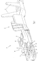
- FIGS. 1 and 2 show, as far as shown in detail, a contact element 1 for a connector.
- a contact element 1 is produced from an electrically conductive material, for example in a stamping and bending process from a flat starting material.
- the contact element 1 has a crimping area 2 with which it is attached to an electrical conductor of a line.
- the outer jacket of the line is passed between two wings 3, which are bent over after the electrical conductor has been fixed in the crimping area 2 in order to create strain relief in this way.
- the crimping area 2 it is conceivable not to make electrical contact with the electrical conductor, or not only by a mechanical crimping process, but also by other methods, such as soldering, for example.
- the wings 3 for the purpose of strain relief can, but need not be present.
- the contact element 1 has a contact area 4 which is designed as follows.
- first base part 5 which, in its axial extension, can, but does not have to, have slots that are transverse thereto.
- first resilient contact part 6 is implemented, for example, by a bending process.
- second fixed base part 7 is present.
- second resilient contact part 8 is provided on the second stationary base part 7.
- the second fixed base part 7 can also have in its axial course at least one or more transversely aligned slots.
- Both the first base part 5 and the second base part 7 are thus designed to be fixed to one another, also with regard to the entire contact element 1, since they are connected to one another via a vertically aligned connecting part 9.
- the two contact parts 6, 8 are designed to be resilient in that their one end extends from the first base part 5 and the second base part 7 into the interior of the contact area 4. This extension is realized in that a tab-shaped structure is bent over by approximately 180 ° from the base parts 5, 7, so that the contact parts 6, 8 are thereby created.
- the respective free end of the contact parts 6, 8 can be limited by the associated areas of the fixed base parts 5, 7.
- the two contact parts 6, 8 are designed in a wave-like manner, with this configuration in each case resulting in two wave crests which each form a contact point 10 for the mating contact element.
- One base part namely the second base part 7, also has an angled area 11 in its one end area.
- This area 11 forms a type of latching lug with which the contact element 1 is fixed in a contact chamber, not shown, in a connector, also not shown.
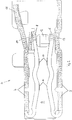
- FIG 2 shows in section the contact area 4 according to Figure 1 , a contact pin 12 being shown schematically as a mating contact element.
- this contact pin 12 is present within the entire contact area 4 and is electrically contacted due to the contact points 10. If the mating contact element, in particular the contact pin 12, has come to rest in the contact area 4 between the contact points 10, then Due to the wave-shaped geometry and the resilient design of the contact parts 6, 8, their free end regions come into contact with a stop 13 on the first fixed base part 5 and with a stop 14 on the second fixed base part 7. On the one hand, this increases the contact forces when the mating contact element, in particular the contact pin 12, is located completely in the contact area 4.
- the mating contact element is preferably located completely in the contact area 4 when its free end reaches the second (when viewing the Figure 2 has passed over the right wave crest with the associated contact points 10). This means that, for example, when looking at the contact pin Figure 2 is introduced from left to right into the contact area 4 and initially the first, that is, when looking at the Figure 2 the left contact point 10 sweeps over. If it is introduced further into the contact area 4, it also passes over the right contact point 10, whereby at the beginning of the introduction of the contact element into the contact area 4, the free ends of the two contact parts 6, 8 did not yet come to rest on the stops 13, 14.
- the contact element according to the invention is characterized on the one hand by the fact that it has a crimping area with which it is attached to the electrical conductor of the line.
- the contact element according to the invention has a contact geometry for a mating contact element, this contact geometry being present twice.
- This contact geometry in particular for a contact pin as a mating contact element, has a wave-shaped profile, the wave shape being selected so that two wave crests point in the direction of the mating contact element, in particular the contact pin, and these wave crests therefore rest on the mating contact element.
- a latching element is formed by the contact area with which the contact element in the contact chamber of the Connector is arranged latching.
- the two mutually facing contact lugs of the contact element which have the wave shape, are arranged pointing from the insertion area of the mating contact element in the plug-in direction backwards in the direction of the crimping area and run approximately parallel to each other.
- Above one end of the contact tab there is an angled area which forms the latching lug for latching the contact element in the contact chamber of the connector.
- the entire contact element consists of an electrically conductive material, for example a corresponding sheet metal material, which is initially designed flat and is fed to a stamping-bending process so that the entire contact element can be produced in one piece with the help of the stamping-bending process.
- an electrically conductive material for example a corresponding sheet metal material
- stamping-bending process so that the entire contact element can be produced in one piece with the help of the stamping-bending process.
Landscapes
- Coupling Device And Connection With Printed Circuit (AREA)
Description
- Die Erfindung betrifft ein Kontaktelement für einen Steckverbinder.
- Ausgangspunkt als Stand der Technik ist die
DE 10 2006 053 152 B3 .US 4 472 017 A offenbart die Merkmale des Oberbegriffes des Anspruchs 1. Das Kontaktelement aus diesem bekannten Stand der Technik weist zwar auch ein erstes Basisteil auf, jedoch ist dieses Basisteil mit zwei Wellenbergen versehen. Dem ersten Basisteil ist ein zweites Basisteil, ebenfalls mit zwei Wellenbergen, zugeordnet. An diesem zweiten Basisteil ist eine Rastfeder-Materiallage angefügt, mit der das Kontaktelement in einer Kontaktkammer eines Steckverbinders festgelegt wird. Insgesamt bietet das aus diesem Stand der Technik bekannte Kontaktelement zwar einen Aufbau, der hinsichtlich der Montage und der Kontaktsicherheit ausreichend, jedoch verbesserungsfähig ist. - Demgegenüber ist es Aufgabe der Erfindung, ein verbessertes Kontaktelement für eine Steckverbindung bereitzustellen.
- Grundsätzlich ist ein Steckverbinder derart aufgebaut, dass er ein Gehäuse aufweist, das zumindest eine, meistens mehrere Kontaktkammern aufweist. In diese Kontaktkammern werden Kontaktelemente eingesetzt und in dieser Kontaktkammer einmal, oftmals auch zweifach verrastet. Das Kontaktelement selber ist am Ende einer elektrischen Leitung angeordnet, wobei ein elektrischer Leiter der Leitung mit dem Kontaktelement elektrisch kontaktiert ist, zum Beispiel durch Verlöten, Vercrimpen oder dergleichen.
- Diese Aufgabe ist durch die Merkmale des Patentanspruches 1 gelöst.
- Erfindungsgemäß ist vorgesehen, dass in einem Kontaktbereich das Kontaktelement eine federnde Kontaktgeometrie für ein Gegenkontaktelement aufweist, wobei diese Kontaktgeometrie doppelt vorhanden ist. Dadurch wird zum einen der Kräfteaufwand, der erforderlich ist, um das Gegenkontaktelement in den Kontaktbereich einzuführen, verringert, weil beide Kontaktgeometrien federnd ausgebildet sind. Diese federnde Ausbildung der Kontaktgeometrie hat darüber hinaus den Vorteil, dass dauerhaft ausreichende Kontaktkräfte auf das Gegenkontaktelement wirken, sodass ein zuverlässiger elektrischer Kontakt zwischen dem Kontaktbereich des Kontaktelementes und dem Gegenkontaktelement realisiert ist.
- In Weiterbildung der Erfindung weist diese Kontaktgeometrie einen wellenförmigen Verlauf auf. In besonders vorteilhafter Weise ist der wellenförmige Verlauf der federnden Kontaktgeometrie symmetrisch (im Schnitt des Kontaktelementes betrachtet) ausgebildet. Dadurch erhöht sich in vorteilhafter Weise die Kontaktsicherheit in einem deutlich größeren Maße, als wenn sich Kontaktpunkte eines wellenförmigen Verlaufes einer Kontaktgeometrie in der Art und Weise gegenüberstehen, dass der eine Wellenberg fest und der andere Wellenberg, der gegenüber liegt, federnd ausgebildet ist.
- In Weiterbildung der Erfindung ist vorgesehen, dass der Kontaktbereich gebildet ist von einem Basisteil, von dem ein erster federnder Kontaktteil ausgeht, sowie einem zweiten feststehenden Basisteil, von dem ein zweiter federnder Kontaktteil ausgeht, wobei die beiden Basisteile über ein senkrecht dazu ausgerichtetes Verbindungsteil miteinander verbunden sind. Diese Ausgestaltung hat einerseits den Vorteil, dass ein solches Kontaktelement in einem üblichen Verfahren, wie zum Beispiel einem Stanz-Biege-Verfahren, schnell, kostengünstig und rationell hergestellt werden kann. Gleichzeitig lässt sich damit eine gegenüber dem Stand der Technik deutlich verbesserte Kontaktgeometrie realisieren, indem zwei feststehende Basisteile ausgebildet werden, an denen jeweils ein federnder Kontaktteil absteht, und die beiden Basisteile über ein senkrecht dazu ausgerichtetes Verbindungsteil miteinander verbunden sind.
- In Weiterbildung der Erfindung ist an einem Ende des zweiten Basisteiles ein abgewinkelter Bereich vorgesehen. Mit diesem abgewinkelten Bereich wird das Kontaktelement zumindest einmal in der Kontaktkammer des Steckverbinders festgelegt, wenn es dort hineinbewegt, insbesondere hineingeschoben wurde. Dadurch lässt sich die Montage eines solchen verbesserten Steckverbinders auch weiterhin verbessern.
- Im Folgenden wird die Erfindung anhand eines Ausführungsbeispieles näher erläutert.
- Die
Figuren 1 und2 zeigen, soweit im Einzelnen dargestellt, ein Kontaktelement 1 für einen Steckverbinder. Ein solches Kontaktelement 1 wird aus einem elektrisch leitenden Material zum Beispiel in einem Stanz-Biege-Verfahren aus einem flächigen Ausgangsmaterial hergestellt. - Das Kontaktelement 1 weist einen Crimpbereich 2 auf, mit dem es an einem elektrischen Leiter einer Leitung angeschlagen wird. Der äußere Mantel der Leitung wird zwischen zwei Flügeln 3 hindurchgeführt, die nach der Festlegung des elektrischen Leiters im Crimpbereich 2 umgebogen werden, um auf diese Art und Weise eine Zugentlastung zu schaffen. Anstelle des Crimpbereiches 2 ist es denkbar, den elektrischen Leiter nicht oder nicht nur durch einen mechanischen Crimpvorgang, sondern auch durch andere Methoden, wie zum Beispiel durch Löten, mit dem Kontaktelement elektrisch zu kontaktieren. Die Flügel 3 zwecks Zugentlastung können, müssen aber nicht vorhanden sein.
- Das Kontaktelement 1 weist einen Kontaktbereich 4 auf, der wie folgt gestaltet ist.
- Ausgehend von dem Crimpbereich 2 ist ein feststehendes erstes Basisteil 5 vorhanden, welches in seiner axialen Erstreckung dazu querliegende Schlitze aufweisen kann, aber nicht muss. Ausgehend von dem ersten Basisteil 5 (genauer an dem dem Crimpbereich abgewandten Ende) ist ein erstes federndes Kontaktteil 6 vorhanden. Dieses erste federnde Kontaktteil 6 wird zum Beispiel durch einen Umbiegevorgang realisiert. Weiterhin ist ein zweites feststehendes Basisteil 7 vorhanden. An dem zweiten feststehenden Basisteil 7 ist einerseits ein zweites federndes Kontaktteil 8 vorgesehen. Auch das zweite feststehende Basisteil 7 kann in seinem axialen Verlauf zumindest einen oder mehrere quer dazu ausgerichtete Schlitze aufweisen.
- Sowohl das erste Basisteil 5 als auch das zweite Basisteil 7 sind dadurch zueinander feststehend ausgebildet, auch bezüglich des gesamten Kontaktelementes 1, da sie über ein senkrecht ausgerichtetes Verbindungsteil 9 miteinander verbunden sind.
- Die beiden Kontaktteile 6, 8 sind dadurch federnd ausgebildet, dass sie mit ihrem einen Ende sich ausgehend von dem ersten Basisteil 5 bzw. dem zweiten Basisteil 7 in das Innere des Kontaktbereiches 4 hinein erstrecken. Diese Erstreckung wird dadurch realisiert, dass ein laschenförmiges Gebilde von den Basisteilen 5, 7 in etwa um 180° umgebogen wird, sodass dadurch die Kontaktteile 6, 8 entstehen. Das jeweilige freie Ende der Kontaktteile 6, 8 kann durch die zugehörigen Bereiche der feststehenden Basisteile 5, 7 begrenzt werden.
- Die beiden Kontaktteile 6, 8 sind wellenförmig gestaltet, wobei aufgrund dieser Gestaltung jeweils zwei Wellenberge entstehen, die jeweils eine Kontaktstelle 10 für das Gegenkontaktelement bilden.
- Das eine Basisteil, nämlich das zweite Basisteil 7, weist in seinem einen Endbereich noch einen abgewinkelten Bereich 11 auf. Durch diesen Bereich 11 wird eine Art Rastnase gebildet, mit der das Kontaktelement 1 in einer nicht dargestellten Kontaktkammer in einem ebenfalls nicht dargestellten Steckverbinder festgelegt wird.
- In
Figur 1 ist abstehend von dem abgewinkelten Bereich 11 ein Vorsprung vorgesehen, der in eine Öffnung des Verbindungsteiles 9 eingreift. Dadurch wird die Bewegung des abgewinkelten Bereiches 11, der ebenfalls federnd ausgehend von dem zweiten feststehenden Basisteil 7 angeordnet ist, definiert begrenzt. -
Figur 2 zeigt im Schnitt den Kontaktbereich 4 gemäßFigur 1 , wobei schematisch als Gegenkontaktelement ein Kontaktstift 12 dargestellt ist. Im endmontierten Zustand einer Steckverbindung ist dieser Kontaktstift 12 innerhalb des gesamten Kontaktbereiches 4 vorhanden und wird elektrisch aufgrund der Kontaktstellen 10 kontaktiert. Ist das Gegenkontaktelement, insbesondere der Kontaktstift 12, im Kontaktbereich 4 zwischen den Kontaktstellen 10 zur Anlage gekommen, wird aufgrund der wellenförmigen Geometrie und der federnden Ausgestaltung der Kontaktteile 6, 8 bewirkt, dass diese mit ihren freien Endbereichen zum einen an einem Anschlag 13 an dem ersten feststehenden Basisteil 5 und zum anderen an einem Anschlag 14 des zweiten feststehenden Basisteiles 7 zur Anlage kommen. Dadurch erhöhen sich zum Einen die Kontaktkräfte, wenn das Gegenkontaktelement, insbesondere der Kontaktstift 12, sich vollständig im Kontaktbereich 4 befindet. Das Gegenkontaktelement befindet sich vorzugsweise dann vollständig in dem Kontaktbereich 4, wenn sein freies Ende den zweiten (bei Betrachtung derFigur 2 den rechten Wellenberg mit den zugehörigen Kontaktstellen 10) überstrichen hat. Das bedeutet, dass beispielsweise der Kontaktstift bei Betrachtung derFigur 2 von links nach rechts in den Kontaktbereich 4 eingeführt wird und zunächst die erste, das heißt bei Betrachtung derFigur 2 die linke Kontaktstelle 10 überstreicht. Wird es weiter in den Kontaktbereich 4 eingeführt, überstreicht es auch die rechte Kontaktstelle 10, wobei zu Beginn des Einführens des Kontaktelementes in den Kontaktbereich 4 die freien Enden der beiden Kontaktteile 6, 8 noch nicht an den Anschlägen 13, 14 zur Anlage kamen. Erst wenn die beiden Kontaktstellen 10 überstrichen worden sind und das Gegenkontaktelement (Kontaktstift 12) seine Endlage erreicht hat, werden die freien Enden der beiden Kontaktteile 6, 8 gegen die Anschläge 13, 14 gedrückt, was bewirkt, dass zunächst während des Einführens des Gegenkontaktelementes in den Kontaktbereich 4 die Kräfte geringer waren als sie weiterhin danach nötig sind, um das Gegenkontaktelement in seine Endposition zu bringen. Dadurch wird das Gegenkontaktelement nicht nur verbessert dauerhaft kontaktiert, sondern auch verbessert mechanisch in dem Kontaktbereich 4 festgelegt. - Das erfindungsgemäße Kontaktelement zeichnet sich mit anderen Worten zum Einen dadurch aus, dass es einen Crimpbereich aufweist, mit dem es an dem elektrischen Leiter der Leitung angeschlagen wird. Im Kontaktbereich weist das erfindungsgemäße Kontaktelement eine Kontaktgeometrie für ein Gegenkontaktelement auf, wobei diese Kontaktgeometrie doppelt vorhanden ist. Diese Kontaktgeometrie, insbesondere für einen Kontaktstift als Gegenkontaktelement weist einen wellenförmigen Verlauf auf, wobei die Wellenform so gewählt ist, dass zwei Wellenberge in Richtung des Gegenkontaktelementes, insbesondere des Kontaktstiftes, weisen und somit diese Wellenberge an dem Gegenkontaktelement anliegen. Gleichzeitig wird von dem Kontaktbereich ein Rastelement gebildet, mit dem das Kontaktelement in der Kontaktkammer des Steckverbinders rastend angeordnet wird. Die beiden zueinander weisenden Kontaktfahnen des Kontaktelementes, die die Wellenform aufweisen, sind vom Einführbereich des Gegenkontaktelementes in Steckrichtung nach hinten in Richtung des Crimpbereiches weisend angeordnet und in etwa parallel zueinander verlaufend. Oberhalb des einen Endes der Kontaktfahne befindet sich ein abgewinkelter Bereich, der die Rastnase zur Verrastung des Kontaktelementes in der Kontaktkammer des Steckverbinders bildet.
- Das gesamte Kontaktelement besteht aus einem elektrisch leitfähigen Material, zum Beispiel einem entsprechenden Blechmaterial, welches zunächst flächig gestaltet ist und einem Stanz-Biege-Verfahren zugeführt wird, so dass das gesamte Kontaktelement einstückig mit Hilfe des Stanz-Biege-Verfahrens hergestellt werden kann. Alternativ dazu ist es denkbar, insbesondere die Kontaktfahnen und / oder den Rastbereich als separate Elemente auszubilden, die entsprechend nach ihrer Herstellung zu einem einteiligen Kontaktelement zusammengefügt werden.
-
- 1.
- Kontaktelement
- 2.
- Crimpbereich
- 3.
- Flügel
- 4.
- Kontaktbereich
- 5.
- Basisteil
- 6.
- Erster Kontaktteil
- 7.
- Zweites Basisteil
- 8.
- Zweiter Kontaktteil
- 9.
- Verbindungsteil
- 10.
- Kontaktstelle
- 11.
- Abgewinkelter Bereich
- 12.
- Kontaktstift
- 13.
- Anschlag
- 14.
- Anschlag
Claims (1)
- Kontaktelement (1) für einen Steckverbinder, das einen Crimpbereich (2) aufweist, mit dem es an einem elektrischen Leiter einer Leitung angeschlagen wird, wobei in einem Kontaktbereich (4) das Kontaktelement (1) derart eine federnde doppelte Kontaktgeometrie für ein Gegenkontaktelement aufweist, dass der Kontaktbereich (4) gebildet ist von einem Basisteil (5), von dem ein erster federnder Kontaktteil (6) ausgeht, sowie einem zweiten feststehenden Basisteil (7), von dem ein zweiter federnder Kontaktteil (8) ausgeht, wobei die beiden Basisteile (5, 7) über ein senkrecht dazu ausgerichtetes Verbindungsteil (9) miteinander verbunden sind, dadurch gekennzeichnet, dass an dem ersten feststehenden Basisteil (5) ein Anschlag (13) und an dem zweiten feststehenden Basisteil (7) ein Anschlag (14) vorgesehen ist, wobei die Kontaktteile (6, 8) mit ihren freien Endbereichen an den Anschlägen (13, 14) zur Anlage kommen, wenn das Gegenkontaktelement in das Kontaktelement (1) eingesetzt ist, und die beiden Kontaktteile (6, 8) wellenförmig gestaltet sind, wobei aufgrund dieser Gestaltung jeweils zwei Wellenberge entstehen, die jeweils eine Kontaktstelle (1) für das Gegenkontaktelement bilden.
Applications Claiming Priority (1)
| Application Number | Priority Date | Filing Date | Title |
|---|---|---|---|
| DE102013218685 | 2013-09-18 |
Publications (2)
| Publication Number | Publication Date |
|---|---|
| EP2852003A1 EP2852003A1 (de) | 2015-03-25 |
| EP2852003B1 true EP2852003B1 (de) | 2020-11-04 |
Family
ID=51564551
Family Applications (1)
| Application Number | Title | Priority Date | Filing Date |
|---|---|---|---|
| EP14185363.0A Active EP2852003B1 (de) | 2013-09-18 | 2014-09-18 | Kontaktelement für einen Steckverbinder |
Country Status (3)
| Country | Link |
|---|---|
| EP (1) | EP2852003B1 (de) |
| DE (1) | DE102014113490A1 (de) |
| ES (1) | ES2832599T3 (de) |
Families Citing this family (8)
| Publication number | Priority date | Publication date | Assignee | Title |
|---|---|---|---|---|
| DE102015201381A1 (de) * | 2014-01-27 | 2015-07-30 | Hirschmann Automotive Gmbh | Kontaktelement |
| CN106025593B (zh) * | 2016-05-12 | 2024-05-28 | 上海友邦电气(集团)股份有限公司 | 一种快插结构 |
| DE102016221351A1 (de) * | 2016-10-28 | 2018-05-03 | Te Connectivity Germany Gmbh | Flachkontaktbuchse mit Ausleger |
| DE102016123163B4 (de) * | 2016-11-30 | 2023-08-31 | Lear Corporation | Elektrische Anschlussbuchse |
| DE102018106646A1 (de) | 2017-03-22 | 2018-09-27 | Hirschmann Automotive Gmbh | Kontaktelement für einen Steckverbinder |
| FR3072833B1 (fr) * | 2017-10-19 | 2020-09-11 | Delphi Int Operations Luxembourg Sarl | Cage de contact electrique femelle |
| CN111430966B (zh) * | 2020-03-20 | 2021-07-20 | 番禺得意精密电子工业有限公司 | 电连接器和连接端子 |
| CN114156671B (zh) * | 2021-12-02 | 2025-11-11 | 长春捷翼汽车科技股份有限公司 | 金属簧片结构及电连接器 |
Citations (1)
| Publication number | Priority date | Publication date | Assignee | Title |
|---|---|---|---|---|
| US4472017A (en) * | 1983-04-01 | 1984-09-18 | Essex Group, Inc. | Tab receptacle terminal |
Family Cites Families (3)
| Publication number | Priority date | Publication date | Assignee | Title |
|---|---|---|---|---|
| DE102005033696B4 (de) * | 2004-07-29 | 2023-06-22 | Te Connectivity Germany Gmbh | Kontaktelement |
| DE102004052378B4 (de) * | 2004-10-28 | 2008-06-19 | Kostal Kontakt Systeme Gmbh | Elektrischer Steckverbinder für ein Kraftfahrzeug |
| DE102006053152B3 (de) | 2006-11-10 | 2008-04-10 | Tyco Electronics Amp Gmbh | Elektrischer Buchsenkontakt |
-
2014
- 2014-09-18 DE DE102014113490.7A patent/DE102014113490A1/de not_active Ceased
- 2014-09-18 EP EP14185363.0A patent/EP2852003B1/de active Active
- 2014-09-18 ES ES14185363T patent/ES2832599T3/es active Active
Patent Citations (1)
| Publication number | Priority date | Publication date | Assignee | Title |
|---|---|---|---|---|
| US4472017A (en) * | 1983-04-01 | 1984-09-18 | Essex Group, Inc. | Tab receptacle terminal |
Also Published As
| Publication number | Publication date |
|---|---|
| DE102014113490A1 (de) | 2015-03-19 |
| ES2832599T3 (es) | 2021-06-10 |
| EP2852003A1 (de) | 2015-03-25 |
Similar Documents
| Publication | Publication Date | Title |
|---|---|---|
| EP2852003B1 (de) | Kontaktelement für einen Steckverbinder | |
| EP2810341B1 (de) | Hülsenkontakt für einen elektrischen nullkraftsteckverbinder | |
| WO2011113594A1 (de) | Hochstromsteckverbinder | |
| EP2243198B1 (de) | Koaxialwinkelsteckverbinder | |
| EP2187480A2 (de) | Steckbuchse für Leiterplatten | |
| EP3482460B1 (de) | Elektrischer hochleistungskontakt | |
| DE10005297A1 (de) | Kontaktstück für eine elektrische Steckverbindung sowie Verfahren zu dessen Herstellung | |
| DE102007055040A1 (de) | Kontaktelement und Verfahren zur Herstellung eines Kontaktelementes | |
| DE102016102036B4 (de) | Elektrischer Steckkontakt, elektrische Anschlussklemme und Verfahren zur Herstellung eines elektrischen Steckkontakts | |
| DE102015211725A1 (de) | Verbinderanschluss und Verbinder hiermit | |
| DE102012221384A1 (de) | Buchsenkontakt für Photovoltaikanwendungen | |
| EP2936617A1 (de) | Mehrfachanschlusskammer mit strombalken | |
| EP2551963B1 (de) | Elektrisches Anschlusselement | |
| DE102008058203A1 (de) | Steckbuchse für Leiterplatten | |
| DE102016002355A1 (de) | Hülsenkontakt für ein elektrisches Steckverbinderteil | |
| DE2616621A1 (de) | Steckverbinder | |
| AT250468B (de) | Federelement für elektrische Steckverbindungen | |
| DE102012105901A1 (de) | Zugentlastungseinheit für einen elektrischen Steckverbinder und Gerätegehäuse | |
| DE102011052387A1 (de) | Federdruckstück zur Herstellung eines elektrischen Federkontaktelements und elektrischer Steckverbinder | |
| DE102005054590A1 (de) | Elektrischer Steckverbinder | |
| WO2023208923A1 (de) | Seitlicher abgang eines rundkontaktes | |
| DE102014113357B9 (de) | Kontaktsystem aus einem elektrischen Kontaktelement und einer Federklammer | |
| DE102007053725B4 (de) | Schaltungsträger für elektromechanische Bauteile | |
| DE102015106467A1 (de) | Kontaktbuchse für einen elektrischen Steckverbinder | |
| DE102008055117A1 (de) | Elektrische Steckvorrichtung |
Legal Events
| Date | Code | Title | Description |
|---|---|---|---|
| PUAI | Public reference made under article 153(3) epc to a published international application that has entered the european phase |
Free format text: ORIGINAL CODE: 0009012 |
|
| 17P | Request for examination filed |
Effective date: 20140918 |
|
| AK | Designated contracting states |
Kind code of ref document: A1 Designated state(s): AL AT BE BG CH CY CZ DE DK EE ES FI FR GB GR HR HU IE IS IT LI LT LU LV MC MK MT NL NO PL PT RO RS SE SI SK SM TR |
|
| AX | Request for extension of the european patent |
Extension state: BA ME |
|
| R17P | Request for examination filed (corrected) |
Effective date: 20160114 |
|
| RBV | Designated contracting states (corrected) |
Designated state(s): AL AT BE BG CH CY CZ DE DK EE ES FI FR GB GR HR HU IE IS IT LI LT LU LV MC MK MT NL NO PL PT RO RS SE SI SK SM TR |
|
| 17Q | First examination report despatched |
Effective date: 20160531 |
|
| STAA | Information on the status of an ep patent application or granted ep patent |
Free format text: STATUS: EXAMINATION IS IN PROGRESS |
|
| GRAP | Despatch of communication of intention to grant a patent |
Free format text: ORIGINAL CODE: EPIDOSNIGR1 |
|
| STAA | Information on the status of an ep patent application or granted ep patent |
Free format text: STATUS: GRANT OF PATENT IS INTENDED |
|
| RIC1 | Information provided on ipc code assigned before grant |
Ipc: H01R 13/11 20060101AFI20200506BHEP Ipc: H01R 4/18 20060101ALN20200506BHEP Ipc: H01R 13/115 20060101ALI20200506BHEP Ipc: H01R 13/193 20060101ALI20200506BHEP |
|
| INTG | Intention to grant announced |
Effective date: 20200520 |
|
| GRAS | Grant fee paid |
Free format text: ORIGINAL CODE: EPIDOSNIGR3 |
|
| GRAA | (expected) grant |
Free format text: ORIGINAL CODE: 0009210 |
|
| STAA | Information on the status of an ep patent application or granted ep patent |
Free format text: STATUS: THE PATENT HAS BEEN GRANTED |
|
| AK | Designated contracting states |
Kind code of ref document: B1 Designated state(s): AL AT BE BG CH CY CZ DE DK EE ES FI FR GB GR HR HU IE IS IT LI LT LU LV MC MK MT NL NO PL PT RO RS SE SI SK SM TR |
|
| REG | Reference to a national code |
Ref country code: GB Ref legal event code: FG4D Free format text: NOT ENGLISH |
|
| REG | Reference to a national code |
Ref country code: CH Ref legal event code: EP |
|
| REG | Reference to a national code |
Ref country code: AT Ref legal event code: REF Ref document number: 1332037 Country of ref document: AT Kind code of ref document: T Effective date: 20201115 |
|
| REG | Reference to a national code |
Ref country code: RO Ref legal event code: EPE |
|
| REG | Reference to a national code |
Ref country code: DE Ref legal event code: R096 Ref document number: 502014014953 Country of ref document: DE |
|
| REG | Reference to a national code |
Ref country code: IE Ref legal event code: FG4D Free format text: LANGUAGE OF EP DOCUMENT: GERMAN |
|
| REG | Reference to a national code |
Ref country code: NL Ref legal event code: MP Effective date: 20201104 |
|
| PG25 | Lapsed in a contracting state [announced via postgrant information from national office to epo] |
Ref country code: PT Free format text: LAPSE BECAUSE OF FAILURE TO SUBMIT A TRANSLATION OF THE DESCRIPTION OR TO PAY THE FEE WITHIN THE PRESCRIBED TIME-LIMIT Effective date: 20210304 Ref country code: NO Free format text: LAPSE BECAUSE OF FAILURE TO SUBMIT A TRANSLATION OF THE DESCRIPTION OR TO PAY THE FEE WITHIN THE PRESCRIBED TIME-LIMIT Effective date: 20210204 Ref country code: FI Free format text: LAPSE BECAUSE OF FAILURE TO SUBMIT A TRANSLATION OF THE DESCRIPTION OR TO PAY THE FEE WITHIN THE PRESCRIBED TIME-LIMIT Effective date: 20201104 Ref country code: RS Free format text: LAPSE BECAUSE OF FAILURE TO SUBMIT A TRANSLATION OF THE DESCRIPTION OR TO PAY THE FEE WITHIN THE PRESCRIBED TIME-LIMIT Effective date: 20201104 Ref country code: GR Free format text: LAPSE BECAUSE OF FAILURE TO SUBMIT A TRANSLATION OF THE DESCRIPTION OR TO PAY THE FEE WITHIN THE PRESCRIBED TIME-LIMIT Effective date: 20210205 |
|
| PG25 | Lapsed in a contracting state [announced via postgrant information from national office to epo] |
Ref country code: LV Free format text: LAPSE BECAUSE OF FAILURE TO SUBMIT A TRANSLATION OF THE DESCRIPTION OR TO PAY THE FEE WITHIN THE PRESCRIBED TIME-LIMIT Effective date: 20201104 Ref country code: IS Free format text: LAPSE BECAUSE OF FAILURE TO SUBMIT A TRANSLATION OF THE DESCRIPTION OR TO PAY THE FEE WITHIN THE PRESCRIBED TIME-LIMIT Effective date: 20210304 Ref country code: PL Free format text: LAPSE BECAUSE OF FAILURE TO SUBMIT A TRANSLATION OF THE DESCRIPTION OR TO PAY THE FEE WITHIN THE PRESCRIBED TIME-LIMIT Effective date: 20201104 Ref country code: SE Free format text: LAPSE BECAUSE OF FAILURE TO SUBMIT A TRANSLATION OF THE DESCRIPTION OR TO PAY THE FEE WITHIN THE PRESCRIBED TIME-LIMIT Effective date: 20201104 Ref country code: BG Free format text: LAPSE BECAUSE OF FAILURE TO SUBMIT A TRANSLATION OF THE DESCRIPTION OR TO PAY THE FEE WITHIN THE PRESCRIBED TIME-LIMIT Effective date: 20210204 |
|
| REG | Reference to a national code |
Ref country code: LT Ref legal event code: MG9D Ref country code: ES Ref legal event code: FG2A Ref document number: 2832599 Country of ref document: ES Kind code of ref document: T3 Effective date: 20210610 |
|
| PG25 | Lapsed in a contracting state [announced via postgrant information from national office to epo] |
Ref country code: HR Free format text: LAPSE BECAUSE OF FAILURE TO SUBMIT A TRANSLATION OF THE DESCRIPTION OR TO PAY THE FEE WITHIN THE PRESCRIBED TIME-LIMIT Effective date: 20201104 |
|
| PG25 | Lapsed in a contracting state [announced via postgrant information from national office to epo] |
Ref country code: SK Free format text: LAPSE BECAUSE OF FAILURE TO SUBMIT A TRANSLATION OF THE DESCRIPTION OR TO PAY THE FEE WITHIN THE PRESCRIBED TIME-LIMIT Effective date: 20201104 Ref country code: LT Free format text: LAPSE BECAUSE OF FAILURE TO SUBMIT A TRANSLATION OF THE DESCRIPTION OR TO PAY THE FEE WITHIN THE PRESCRIBED TIME-LIMIT Effective date: 20201104 Ref country code: EE Free format text: LAPSE BECAUSE OF FAILURE TO SUBMIT A TRANSLATION OF THE DESCRIPTION OR TO PAY THE FEE WITHIN THE PRESCRIBED TIME-LIMIT Effective date: 20201104 Ref country code: SM Free format text: LAPSE BECAUSE OF FAILURE TO SUBMIT A TRANSLATION OF THE DESCRIPTION OR TO PAY THE FEE WITHIN THE PRESCRIBED TIME-LIMIT Effective date: 20201104 |
|
| REG | Reference to a national code |
Ref country code: DE Ref legal event code: R097 Ref document number: 502014014953 Country of ref document: DE |
|
| PG25 | Lapsed in a contracting state [announced via postgrant information from national office to epo] |
Ref country code: DK Free format text: LAPSE BECAUSE OF FAILURE TO SUBMIT A TRANSLATION OF THE DESCRIPTION OR TO PAY THE FEE WITHIN THE PRESCRIBED TIME-LIMIT Effective date: 20201104 |
|
| PLBE | No opposition filed within time limit |
Free format text: ORIGINAL CODE: 0009261 |
|
| STAA | Information on the status of an ep patent application or granted ep patent |
Free format text: STATUS: NO OPPOSITION FILED WITHIN TIME LIMIT |
|
| 26N | No opposition filed |
Effective date: 20210805 |
|
| PG25 | Lapsed in a contracting state [announced via postgrant information from national office to epo] |
Ref country code: NL Free format text: LAPSE BECAUSE OF FAILURE TO SUBMIT A TRANSLATION OF THE DESCRIPTION OR TO PAY THE FEE WITHIN THE PRESCRIBED TIME-LIMIT Effective date: 20201104 Ref country code: AL Free format text: LAPSE BECAUSE OF FAILURE TO SUBMIT A TRANSLATION OF THE DESCRIPTION OR TO PAY THE FEE WITHIN THE PRESCRIBED TIME-LIMIT Effective date: 20201104 |
|
| PG25 | Lapsed in a contracting state [announced via postgrant information from national office to epo] |
Ref country code: SI Free format text: LAPSE BECAUSE OF FAILURE TO SUBMIT A TRANSLATION OF THE DESCRIPTION OR TO PAY THE FEE WITHIN THE PRESCRIBED TIME-LIMIT Effective date: 20201104 |
|
| REG | Reference to a national code |
Ref country code: CH Ref legal event code: PL |
|
| REG | Reference to a national code |
Ref country code: BE Ref legal event code: MM Effective date: 20210930 |
|
| PG25 | Lapsed in a contracting state [announced via postgrant information from national office to epo] |
Ref country code: IS Free format text: LAPSE BECAUSE OF FAILURE TO SUBMIT A TRANSLATION OF THE DESCRIPTION OR TO PAY THE FEE WITHIN THE PRESCRIBED TIME-LIMIT Effective date: 20210304 Ref country code: MC Free format text: LAPSE BECAUSE OF FAILURE TO SUBMIT A TRANSLATION OF THE DESCRIPTION OR TO PAY THE FEE WITHIN THE PRESCRIBED TIME-LIMIT Effective date: 20201104 |
|
| PG25 | Lapsed in a contracting state [announced via postgrant information from national office to epo] |
Ref country code: LU Free format text: LAPSE BECAUSE OF NON-PAYMENT OF DUE FEES Effective date: 20210918 Ref country code: IE Free format text: LAPSE BECAUSE OF NON-PAYMENT OF DUE FEES Effective date: 20210918 Ref country code: BE Free format text: LAPSE BECAUSE OF NON-PAYMENT OF DUE FEES Effective date: 20210930 |
|
| PG25 | Lapsed in a contracting state [announced via postgrant information from national office to epo] |
Ref country code: LI Free format text: LAPSE BECAUSE OF NON-PAYMENT OF DUE FEES Effective date: 20210930 Ref country code: CH Free format text: LAPSE BECAUSE OF NON-PAYMENT OF DUE FEES Effective date: 20210930 |
|
| REG | Reference to a national code |
Ref country code: AT Ref legal event code: MM01 Ref document number: 1332037 Country of ref document: AT Kind code of ref document: T Effective date: 20210918 |
|
| PG25 | Lapsed in a contracting state [announced via postgrant information from national office to epo] |
Ref country code: AT Free format text: LAPSE BECAUSE OF NON-PAYMENT OF DUE FEES Effective date: 20210918 |
|
| PG25 | Lapsed in a contracting state [announced via postgrant information from national office to epo] |
Ref country code: HU Free format text: LAPSE BECAUSE OF FAILURE TO SUBMIT A TRANSLATION OF THE DESCRIPTION OR TO PAY THE FEE WITHIN THE PRESCRIBED TIME-LIMIT; INVALID AB INITIO Effective date: 20140918 |
|
| PG25 | Lapsed in a contracting state [announced via postgrant information from national office to epo] |
Ref country code: CY Free format text: LAPSE BECAUSE OF FAILURE TO SUBMIT A TRANSLATION OF THE DESCRIPTION OR TO PAY THE FEE WITHIN THE PRESCRIBED TIME-LIMIT Effective date: 20201104 |
|
| PGFP | Annual fee paid to national office [announced via postgrant information from national office to epo] |
Ref country code: RO Payment date: 20230913 Year of fee payment: 10 Ref country code: GB Payment date: 20230920 Year of fee payment: 10 Ref country code: CZ Payment date: 20230912 Year of fee payment: 10 |
|
| PGFP | Annual fee paid to national office [announced via postgrant information from national office to epo] |
Ref country code: FR Payment date: 20230928 Year of fee payment: 10 |
|
| PGFP | Annual fee paid to national office [announced via postgrant information from national office to epo] |
Ref country code: ES Payment date: 20231124 Year of fee payment: 10 |
|
| PGFP | Annual fee paid to national office [announced via postgrant information from national office to epo] |
Ref country code: IT Payment date: 20230927 Year of fee payment: 10 |
|
| PG25 | Lapsed in a contracting state [announced via postgrant information from national office to epo] |
Ref country code: MK Free format text: LAPSE BECAUSE OF FAILURE TO SUBMIT A TRANSLATION OF THE DESCRIPTION OR TO PAY THE FEE WITHIN THE PRESCRIBED TIME-LIMIT Effective date: 20201104 |
|
| PG25 | Lapsed in a contracting state [announced via postgrant information from national office to epo] |
Ref country code: MT Free format text: LAPSE BECAUSE OF FAILURE TO SUBMIT A TRANSLATION OF THE DESCRIPTION OR TO PAY THE FEE WITHIN THE PRESCRIBED TIME-LIMIT Effective date: 20201104 |
|
| PG25 | Lapsed in a contracting state [announced via postgrant information from national office to epo] |
Ref country code: CZ Free format text: LAPSE BECAUSE OF NON-PAYMENT OF DUE FEES Effective date: 20240918 |
|
| GBPC | Gb: european patent ceased through non-payment of renewal fee |
Effective date: 20240918 |
|
| PG25 | Lapsed in a contracting state [announced via postgrant information from national office to epo] |
Ref country code: GB Free format text: LAPSE BECAUSE OF NON-PAYMENT OF DUE FEES Effective date: 20240918 |
|
| PG25 | Lapsed in a contracting state [announced via postgrant information from national office to epo] |
Ref country code: IT Free format text: LAPSE BECAUSE OF NON-PAYMENT OF DUE FEES Effective date: 20240918 |
|
| PG25 | Lapsed in a contracting state [announced via postgrant information from national office to epo] |
Ref country code: FR Free format text: LAPSE BECAUSE OF NON-PAYMENT OF DUE FEES Effective date: 20240930 |
|
| PG25 | Lapsed in a contracting state [announced via postgrant information from national office to epo] |
Ref country code: RO Free format text: LAPSE BECAUSE OF NON-PAYMENT OF DUE FEES Effective date: 20240918 |
|
| PGFP | Annual fee paid to national office [announced via postgrant information from national office to epo] |
Ref country code: DE Payment date: 20250919 Year of fee payment: 12 |
|
| REG | Reference to a national code |
Ref country code: ES Ref legal event code: FD2A Effective date: 20251031 |
|
| PG25 | Lapsed in a contracting state [announced via postgrant information from national office to epo] |
Ref country code: TR Free format text: LAPSE BECAUSE OF FAILURE TO SUBMIT A TRANSLATION OF THE DESCRIPTION OR TO PAY THE FEE WITHIN THE PRESCRIBED TIME-LIMIT Effective date: 20201104 |
|
| PG25 | Lapsed in a contracting state [announced via postgrant information from national office to epo] |
Ref country code: ES Free format text: LAPSE BECAUSE OF NON-PAYMENT OF DUE FEES Effective date: 20240919 |