EP2847664B1 - Data transfer between clock domains - Google Patents
Data transfer between clock domains Download PDFInfo
- Publication number
- EP2847664B1 EP2847664B1 EP13731452.2A EP13731452A EP2847664B1 EP 2847664 B1 EP2847664 B1 EP 2847664B1 EP 13731452 A EP13731452 A EP 13731452A EP 2847664 B1 EP2847664 B1 EP 2847664B1
- Authority
- EP
- European Patent Office
- Prior art keywords
- clock
- clock domain
- bus
- data signal
- domain
- Prior art date
- Legal status (The legal status is an assumption and is not a legal conclusion. Google has not performed a legal analysis and makes no representation as to the accuracy of the status listed.)
- Not-in-force
Links
Images
Classifications
-
- H—ELECTRICITY
- H04—ELECTRIC COMMUNICATION TECHNIQUE
- H04L—TRANSMISSION OF DIGITAL INFORMATION, e.g. TELEGRAPHIC COMMUNICATION
- H04L7/00—Arrangements for synchronising receiver with transmitter
- H04L7/0008—Synchronisation information channels, e.g. clock distribution lines
-
- G—PHYSICS
- G06—COMPUTING OR CALCULATING; COUNTING
- G06F—ELECTRIC DIGITAL DATA PROCESSING
- G06F1/00—Details not covered by groups G06F3/00 - G06F13/00 and G06F21/00
- G06F1/04—Generating or distributing clock signals or signals derived directly therefrom
- G06F1/12—Synchronisation of different clock signals provided by a plurality of clock generators
-
- G—PHYSICS
- G06—COMPUTING OR CALCULATING; COUNTING
- G06F—ELECTRIC DIGITAL DATA PROCESSING
- G06F5/00—Methods or arrangements for data conversion without changing the order or content of the data handled
- G06F5/06—Methods or arrangements for data conversion without changing the order or content of the data handled for changing the speed of data flow, i.e. speed regularising or timing, e.g. delay lines, FIFO buffers; over- or underrun control therefor
-
- G—PHYSICS
- G06—COMPUTING OR CALCULATING; COUNTING
- G06F—ELECTRIC DIGITAL DATA PROCESSING
- G06F13/00—Interconnection of, or transfer of information or other signals between, memories, input/output devices or central processing units
- G06F13/38—Information transfer, e.g. on bus
- G06F13/40—Bus structure
- G06F13/4004—Coupling between buses
- G06F13/4027—Coupling between buses using bus bridges
- G06F13/405—Coupling between buses using bus bridges where the bridge performs a synchronising function
-
- H—ELECTRICITY
- H04—ELECTRIC COMMUNICATION TECHNIQUE
- H04L—TRANSMISSION OF DIGITAL INFORMATION, e.g. TELEGRAPHIC COMMUNICATION
- H04L27/00—Modulated-carrier systems
- H04L27/26—Systems using multi-frequency codes
- H04L27/2601—Multicarrier modulation systems
- H04L27/2647—Arrangements specific to the receiver only
- H04L27/2655—Synchronisation arrangements
-
- H—ELECTRICITY
- H04—ELECTRIC COMMUNICATION TECHNIQUE
- H04B—TRANSMISSION
- H04B1/00—Details of transmission systems, not covered by a single one of groups H04B3/00 - H04B13/00; Details of transmission systems not characterised by the medium used for transmission
- H04B1/69—Spread spectrum techniques
- H04B1/707—Spread spectrum techniques using direct sequence modulation
- H04B1/7073—Synchronisation aspects
-
- H—ELECTRICITY
- H04—ELECTRIC COMMUNICATION TECHNIQUE
- H04B—TRANSMISSION
- H04B1/00—Details of transmission systems, not covered by a single one of groups H04B3/00 - H04B13/00; Details of transmission systems not characterised by the medium used for transmission
- H04B1/69—Spread spectrum techniques
- H04B1/713—Spread spectrum techniques using frequency hopping
- H04B1/7156—Arrangements for sequence synchronisation
Definitions
- This invention relates to systems and methods for transferring data signals between clock domains in digital systems, in particular where the clock domains are not synchronised.
- a central processor may run at a high frequency with one or more peripherals running at a low frequency.
- one of the clock domains may enter periods of inactivity, e.g. a sleep or standby mode, when it is not being used in order to save power. This is typically the faster clock domain, with the slower clock domain being used as a timer during these periods. In these periods there is no communication between the two clock domains, however when the one clock domain exits the sleep or standby mode, it will often need to communicate with the slower clock domain.
- the fast and the slow clock domains may not necessarily be synchronised with each other.
- US 2009/0225915 describes a data communications system comprising two clock domains, each coupled to receive a source clock signal.
- the first clock domain includes a first clock signal and the second clock domain includes a second clock signal, each of the first clock signal and the second clock signal are derived from the source clock signal.
- the first clock signal has a frequency which is different from that of the second clock signal.
- Data is latched only when a pulse is asserted and on a given edge of the first clock signal. The pulse is generated such that the given edge occurs at approximately a position corresponding to a middle of a period of the second clock signal, where this approximate position is determined using a known ratio between the respective frequencies of the first and second clock signals.
- the invention provides an arrangement for transferring a data signal from a first clock domain to a second clock domain in a digital system, wherein the first clock domain comprises a first clock having a frequency less than a frequency of a second clock in the second clock domain, the arrangement being configured to:
- the invention also provides a method of transferring a data signal from a first clock domain to a second clock domain in a digital system, wherein the first clock domain comprises a first clock having a frequency less than a frequency of a second clock in the second clock domain, the method comprising:
- the data signal is simply transferred from the first clock domain to the second clock domain but a check is carried out as to whether or not a clock transition occurred in the first clock within the predetermined period. If a transition is detected, the data signal from the first clock domain is transferred again to the second clock domain, otherwise the initial transfer of the signal is deemed to have been "safe", i.e. there is no risk of meta-stability.
- safe i.e. there is no risk of meta-stability.
- the synchronisation and transfer time is typically at least two first clock cycles, i.e. two slow clock cycles, compared to the synchronisation and transfer time for embodiments of the present invention which can be as little as a few second clock cycles, i.e. a few fast clock cycles.
- the transfer of the data signal subsequent to a transition in the first clock could be at the end of the predetermined period, e.g. at a corresponding transition of the second clock, but preferably occurs at the subsequent transition in the second clock.
- the detecting means could be arranged to detect a positive and/or a negative transition, i.e. the data values in the first clock domain could change on one or both of the positive and negative transitions of the first clock, depending on the implementation of the system and the technology used.
- the transition being detected is a positive transition
- the check of the first clock is made to ensure that its cycle was away from a transition - i.e. either a positive transition from zero to one or a negative transition from one to zero, so that the initial transfer of the data signal from the first clock domain to the second clock domain did not coincide with a transition in the first clock cycle.
- the Applicant has appreciated that because the check of the first clock confirms that the data signal is safe to be transferred either the initial or subsequent transfer of the data signal takes place in a safe part of the first, slow clock cycle.
- the data signal is not transferred from the first clock domain to the second clock domain via any of the synchronisation components in the arrangement, e.g. the detecting means.
- the first clock domain comprises a first bus
- the second clock domain comprises a second bus
- data is transferred from the first bus to the second bus, both initially and if a subsequent transfer is deemed necessary. It also means that embodiments of the invention do not need to introduce the latency associated with serial flip flops or other arrangements typically used to match clock domains in the prior art.
- the data bus comprises at least 8, 16 or 32 bits, though it will be appreciated that the bus could comprise any number of multiple bits.
- a further benefit in reducing power consumption may be achievable with a quicker transfer as it allows one or both of the clocks to go into a sleep state more quickly if appropriate.
- the known handshaking procedures require multiple slower clock cycles to complete, during which the faster clock is kept running. This can consume a significant amount of unnecessary power, especially if the slower clock domain includes a low power low frequency clock and the faster clock domain is high power, which is a common arrangement in a low power device.
- the detection comprises discrete sampling of the first clock based on another clock - preferably the second clock. This enables, in some embodiments, the data signal to be re-transferred, if necessary, as quickly as possible , i.e. the discrete sampling allows the predetermined transition in the first clock to be detected shortly after it occurs so that the data signal can be transferred after this detection.
- the detecting means comprises an edge detector, e.g. a positive edge detector.
- the edge detector is, as mentioned above, conveniently clocked by the second clock.
- the detection of a transition in the first clock requires a finite amount of time: the first clock transition has to enter the detecting means and the resultant logic signals have to be transferred through the detecting means and any other components which may rely on them in order to effect the transfer of the data signal between the first clock domain and the second clock domain.
- the predetermined period over which the detecting means looks for a transition in the first clock is greater than the time taken for a change of signal in the first clock domain to stabilise at a valid value and the time taken for a clock transition to propagate through the detecting means.
- the number of sampling points in the discrete sampling will generally be related to the time taken to propagate these logic signals through the necessary components.
- the predetermined period is between 1 and 16 cycles of the second clock, e.g. between 2 and 8 cycles of the second clock, e.g. 4 cycles of the second clock. However, it is not necessary for the predetermined period to correspond to an integer number of cycles of the second clock, for example if it is clocked by a different clock. If a transition has not been detected in the predetermined period, it can be safely assumed that the initial transfer of the data signal from the first clock domain to the second clock domain did not coincide with a transition in the first clock.
- the elapse of the predetermined period could be timed by any suitable timing mechanism, e.g. a timer or counter.
- the detection of a transition in the first clock comprises a number of steps and/or is carried out over a number of cycles of the second clock. Therefore preferably the detecting means comprises means to count the multiple steps of the discrete sampling and/or the number of cycles in the predetermined period. This could be a component such as a down counter, a gray-code counter, or one or more flip-flops in series.
- the counting means is clocked by the second clock, i.e. synchronised with the detecting means.
- detection of the predetermined transition in the first clock cycle could be performed at any transition (either positive or negative) of the second clock.
- the detection is performed at a rising edge, i.e. positive transition, of the second clock, e.g. this marks the start of the predetermined period.
- the detection may comprise multiple steps, with subsequent steps being performed at a subsequent, e.g. the next, rising edge of the second clock.
- the frequency of the discrete sampling equals the frequency of the second clock, - i.e.
- a sample is carried out on every cycle of the second clock during the detection, in order to detect a transition as soon as possible therefore allowing the fastest possible re-transfer of the data signal if necessary (although this is not essential - it may always wait until the end of the predetermined period to transfer the data again).
- the ratio of the frequency of the second clock to the first clock should be great enough such that it can be guaranteed that a further transition in the first clock will not occur during the time taken to effect the transfer of the data signal from the first clock domain to the second clock domain.
- the frequency of the second clock could be an integer multiple of the frequency of the first clock and/or have a fixed phase, in general no synchronisation or particular relationship is required in accordance with the present invention.
- embodiments of the invention may be tolerant to the first and/or second clock domain entering a sleep or standby mode and restarting asynchronously with respect to the other clock domain.
- the frequency of the second clock is at least four times the frequency, e.g. at least ten times the frequency, e.g. at least one hundred times the frequency, e.g. at least one thousand times the frequency of the first clock.
- this ensures that there is sufficient time to detect and process the predetermined transition and transfer the data again without risk of there being a further transition and the associated risk of data corruption or meta-stability.
- the detecting means is clocked by the second clock
- the frequency of the first clock is 32 kHz and the frequency of the second clock is 16 MHz.
- the detecting means could comprise an edge detector arranged to compare the values at an input on consecutive clock cycles.
- any suitable arrangement depending on the nature of the check could be provided, i.e. any component or arrangement which is able to detect a transition in the first clock. Therefore generally the detecting means will have the first clock as an input.
- the detecting means comprises a flip-flop, e.g. a D-type flip-flop, or a comparator. More than one flip-flop could be provided in series to increase the certainty of the check performed by the flip-flop. There is a small chance that the output from the flip-flop will be in an unstable state that takes some time to resolve itself - e.g.
- the check for a transition in the first clock could be performed all the time, e.g. every cycle of the second clock.
- the system comprises means for initiating the predetermined period. This could be a specific signal which is sent in order for the predetermined period to start, or it could be linked to other signals or cycles in the system.
- the predetermined period could be initiated by a change in the input signal, by the system or second clock domain entering or exiting a standby or sleep mode, or by a central processing unit (CPU) requesting data to be read from the first clock domain.
- CPU central processing unit
- Embodiments in which the detection is initiated rather than being performed continuously are advantageous as they help the system to reduce the power consumption as the checks are only performed when necessary, and allows the second clock domain to go into a sleep mode during the period after the signal has been transferred and before the next transfer of a data signal is needed, thus saving power.
- Embodiments of the present invention may be particularly suited to a mode of operation in which the second clock domain requests a transfer of the data signal from the first clock domain, e.g. when the second clock domain exits a sleep or standby mode and requests a certain data signal - the time, for instance, which provides the signal to start the predetermined period.
- the predetermined period will generally be fixed and last for a set number of second clock cycles following its initiation.
- the transition detection is terminated once a transition in the first clock has been detected and the necessary logic signals to indicate this have passed through the arrangement i.e. before expiry of the predetermined period. This is because once it is indicated that it is safe to transfer the data signal from the first clock domain to the second clock domain again, the fact that the first clock is slower than the second clock guarantees that there will not be a further transition in the first clock when the data signal is transferred again, so there is no point in continuing the detection for any longer than this.
- the transferred data signal can be changed at any time during synchronisation, i.e. during the predetermined period, without affecting the synchronisation process or the resultant re-transfer, if necessary, of the data signal from the first clock domain to the second clock domain, e.g. by causing meta-stability in the output signal.
- This is in contrast to the conventional handshaking procedure in which a freeze is put on the data signal being transferred from the first clock domain, e.g. through the use of busy flags, in order to perform the synchronisation between the first and second clock domains.
- the arrangement simply generates a "safe" synchronisation signal in order to determine whether or not it needs to transfer the data again from the first clock domain to the second clock domain again. It therefore does not matter as to the state of the data signal, which can change during the predetermined period, i.e. it is the value of the data signal in the first clock domain at the end of, or at another time during, the predetermined period which is transferred to the second clock domain if there has been a transition in the first clock cycle, which will generally mean that the value of the data signal will have changed.
- the data signal remains that which was transferred initially as generally this will mean that the data signal has not changed value.
- the most recent data signal in the first clock domain will be transferred to the second clock domain following the transition.
- This freedom to change the data signal in the first clock domain during the predetermined period contrasts with the conventional approach in which the data signal to be transferred is not allowed to be changed during synchronisation of the two clock domains.
- the synchronisation process e.g. handshaking and/or involving busy flags, involves checking of the data signal to be transferred, as well as the clock cycles.
- the system of the present invention is free from these restrictions thus allowing greater freedom in its uses and architecture.
- the system comprises means for storing the data signal, e.g. a storage device or component, with the method comprising the step of storing the data signal.
- a storage device or component e.g. a storage device or component
- the method comprising the step of storing the data signal.
- This allows the data signal to be stored temporarily before it is output to the second clock domain, for either or both of the initial transfer and the subsequent transfer if necessary.
- the data signal could also be stored during the predetermined period, i.e. while the check of the first clock is being made and the logic signals are passing through the detecting means.
- the means for storing the signal input from the first clock domain could comprise any suitable data storage component, arrangement or device which is able to store the data signal during unsafe parts of the first clock cycle and/or during the predetermined period so that the signal is ready to be output to the second clock domain when the check is started and/or after the check of the first clock has been performed.
- This could comprise a register, e.g. a flip-flop or a latch.
- a register e.g. a flip-flop or a latch.
- multiple components may be provided depending on the size of the bus, e.g. multiple flip-flops in parallel.
- Such a component may store the input signal until it receives a signal, e.g. from the detecting means, that it is safe to transfer it to the second clock domain.
- the storing means could receive the data signal from the first clock domain, i.e. the storing means and the first clock domain could comprise separate components: one to receive the input signal and one to store the input signal. However this function could also be performed by the first clock domain which receives and stores the data signal prior to it being transferred.
- the arrangement comprises means to prevent the initially transferred data signal being read by the second clock domain.
- This block on the data signal being read by the second clock domain could comprise a "ready" signal, e.g. set to zero when the block is in place and set to one when the data signal has been determined to be safe and ready to be read by the second clock domain.
- This ready signal could be linked to the detecting means and/or the predetermined period. For example, if the arrangement comprises a timer or counter, the ready signal could be issued at a particular point relative to the predetermined period, such as at the end of the predetermined period.
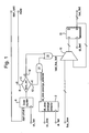
- Fig. 1 shows a schematic logic circuit diagram corresponding to an arrangement embodying the invention.
- the arrangement is arranged to transfer data from a first bus, bus _ slow , in a first clock domain to a second bus, bus _ fast , in a second clock domain.
- the frequency of the first clock, ck_slow is less than the frequency of the second clock, ck_fast, with typical frequencies being 32 kHz for the first clock, ck_slow, and 16 MHz for the second clock, ck_ fast.
- the arrangement comprises a positive edge detector 2 for the first clock, ck_slow, which the positive edge detector 2 takes as its input.
- the output, posedge _ detected , from the positive edge detector 2 is a one if a positive edge in the first clock, ck_slow, has been detected, and a zero otherwise.
- the second clock, ck_fast is used to clock the positive edge detector 2, such that at each rising edge of the second clock, the value of the input, ck_slow, is sampled and compared to its value at the previous rising edge of the second clock.
- the arrangement also comprises a down counter 4, which takes as its input an initialisation signal, start_sync, which indicates that the synchronisation process is to start in order to transfer the data.
- the output, sync _ cnt , from the down counter 4 is the value of the count, which is an integer that is reduced by one at each count. In the embodiment shown in Fig. 1 the count is always started at three.
- the second clock, ck_fast is also used to clock the down counter 4, i.e. at each rising edge of the second clock, the down counter reduces the value of its output, sync _ cnt , by one.
- the output, sync _ cnt , from the down counter 4 is fed to a decision node 6.
- the first output 8 has a value of one if the output, sync _ cnt , from the down counter 4 is equal to zero.
- the second output 10 has a value of one if the output, sync _ cnt , from the down counter 4 is equal to three.
- the third output 12 has a value of one if the output, sync _ cnt , from the down counter 4 is not equal to zero.
- the second and third outputs 10, 12 from the decision node 6 can both have a value of one, i.e. when the output, sync _ cnt , from the down counter 4 has a value of three.
- a signal, ready is output to the system indicating that the data from the first bus, bus _ slow , has been transferred and the arrangement is ready to receive a further initialisation signal, start_sync.
- the output signal, posedge _ detected , from the positive edge detector 2 is combined with the third output 12 from the decision node 6 in an AND gate 14, with the output from the AND gate 14 being combined with the second output 10 from the decision node 6 in an OR gate 16.
- the output, load _ bus _ fast , from the OR gate 16 is fed to the selector input of a multiplexer 18.
- the inputs to the multiplexer 18 are the data signal from the first bus, bus _ slow , and the output data signal to the second bus, bus _ fast .
- the output from the multiplexer 18 is fed to a D-type flip-flop 20 which is clocked by the second clock, ck_fast.
- the Q output from the flip-flop 20 is the output to the second bus, bus _ fast .
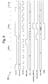
- FIG. 1 shows the sequence of logic signals passing through the system.
- a representative time scale 22 is given in subdivisions of 50 ns.
- the frequency of the second clock, ck_fast, from the second, higher frequency, clock domain 4 is taken to be 16 MHz and the frequency of the first clock, ck_slow, from the first, lower frequency, clock domain 8, is taken to be 1.5 MHz.
- ck_fast the frequency of the second clock
- ck_slow from the first, lower frequency, clock domain 8
- the system is in a state in which the multi-bit data h9 (a hex value) is in the first bus, bus _ slow , and the second bus, bus _ fast , is unknown, i.e. the value in the bus is that from the previous transfer.
- the system is in a steady state until at 565 ns the initialisation signal, start_sync, changes from zero to one, thus triggering the start of the synchronisation process.
- the initialisation signal will be generated by the second clock domain (generally controlling a higher power peripheral device) when it exits a sleep mode in order to request transfer of the data from the first clock domain (generally a lower power timing circuit).
- the down counter 4 is clocked by the next rising edge of the second clock, ck_fast, causing it to start counting down from three, i.e. at 625 ns the output, sync _ cnt , from the down counter 4 changes to three. It is necessary for the down counter 4 to count down from three because the positive edge detector 2 takes two cycles of the second clock, ck_fast, for a positive transition to be detected, i.e. for the necessary logic signals to be passed through its flip-flops.
- This output value of three for sync _ cnt from the down counter 4 causes the first output 8 of the decision node 6 to have a value of zero and the second and third outputs 10, 12 of the decision node 6 to have a value of one. Regardless of the output, posedge _ detected , from the positive edge detector 2, these inputs to the OR gate 16 cause the output, load_bus_fast, from the OR gate 16 to have a value of one.
- This value of one which is fed to the selector input of the multiplexer 18 causes the data signal h9 in the first bus, bus _ slow , to be fed to the D input of the flip-flop 20, such that on the next rising edge of the second clock, ck_fast, the data signal h9 is transferred to the second bus, bus _ fast .
- the positive edge detector 2 checks for a positive transition in the cycle of the first clock, ck_slow.
- the first clock, ck_slow has a positive transition. In this example this transition is associated with a change in the data signal in the first bus, bus _ slow , from h9 to hC, but in other situations the data signal may remain the same.
- the output, posedge _ detected from the positive edge detector 2 changes to one, indicating that the positive transition in the first clock, ck_slow, has been detected.
- This value of one combined with the value of one from the third output 12 from the decision node 6 (i.e. at this point the output, sync_cnt, from the down counter 4 is one, which is not equal to zero), causes the AND gate 14 to have an output value of one, and also the OR gate 16 to have an output value, load_bus_fast, of one.
- a load_bus_fast value of one which is fed to the selector input of the multiplexer 18 causes the data signal, which is now hC, in the first bus, bus _ slow , to be fed to the D input of the flip-flop 20, such that on the next rising edge of the second clock, ck_fast, the data signal hC is transferred to the second bus, bus _ fast .
- the frequency of the first clock, ck_slow is sufficiently low to ensure that the transfer of the data signal is completed before a further positive transition in the first clock will occur.
- sync _ cnt from the down counter 4 has reached zero, which causes the value of the first output 8 from the decision node 6 to be one, indicating that the system is ready to receive a new initialisation signal, i.e. the signal, ready, is equal to one.
- the data signal stored in the flip-flop 20 is a valid and stable value which can then be used in the system as data synchronised to the second clock, ck_fast, e.g. output to the second bus, bus _ fast , at this rising edge of the second clock, ck_fast, as described above.
- the second and third outputs 10, 12 from the decision node 6 are zero when the output, sync _ cnt , from the down counter 4 is zero, so no new data signal can be transferred from the first bus, bus _ slow , to the flip-flop 20 at this time. Therefore, in an embodiment (not shown), in which a positive transition does not occur within the predetermined period, i.e.
- the length of the predetermined period could be a different value, particularly if this depends on the type of component used to detect a transition in the first clock, i.e. the time taken to get a decision out of this component, or if one or more of the components are clocked on both transitions of the second clock.
Landscapes
- Engineering & Computer Science (AREA)
- Theoretical Computer Science (AREA)
- General Engineering & Computer Science (AREA)
- Physics & Mathematics (AREA)
- General Physics & Mathematics (AREA)
- Computer Networks & Wireless Communication (AREA)
- Signal Processing (AREA)
- Computer Hardware Design (AREA)
- Information Transfer Systems (AREA)
- Synchronisation In Digital Transmission Systems (AREA)
- Manipulation Of Pulses (AREA)
Applications Claiming Priority (2)
| Application Number | Priority Date | Filing Date | Title |
|---|---|---|---|
| GB1211425.2A GB2503473A (en) | 2012-06-27 | 2012-06-27 | Data transfer from lower frequency clock domain to higher frequency clock domain |
| PCT/GB2013/051608 WO2014001765A1 (en) | 2012-06-27 | 2013-06-20 | Data transfer between clock domains |
Publications (2)
| Publication Number | Publication Date |
|---|---|
| EP2847664A1 EP2847664A1 (en) | 2015-03-18 |
| EP2847664B1 true EP2847664B1 (en) | 2018-04-18 |
Family
ID=46704315
Family Applications (1)
| Application Number | Title | Priority Date | Filing Date |
|---|---|---|---|
| EP13731452.2A Not-in-force EP2847664B1 (en) | 2012-06-27 | 2013-06-20 | Data transfer between clock domains |
Country Status (8)
| Country | Link |
|---|---|
| US (1) | US9515812B2 (enExample) |
| EP (1) | EP2847664B1 (enExample) |
| JP (1) | JP6192065B2 (enExample) |
| KR (1) | KR20150037900A (enExample) |
| CN (1) | CN104412222B (enExample) |
| GB (1) | GB2503473A (enExample) |
| TW (1) | TWI604689B (enExample) |
| WO (1) | WO2014001765A1 (enExample) |
Families Citing this family (5)
| Publication number | Priority date | Publication date | Assignee | Title |
|---|---|---|---|---|
| GB2528481B (en) | 2014-07-23 | 2016-08-17 | Ibm | Updating of shadow registers in N:1 clock domain |
| GB201907717D0 (en) * | 2019-05-31 | 2019-07-17 | Nordic Semiconductor Asa | Apparatus and methods for dc-offset estimation |
| TWI740564B (zh) * | 2020-07-03 | 2021-09-21 | 鴻海精密工業股份有限公司 | 跨時鐘域信號傳輸方法、電路以及電子裝置 |
| GB202014083D0 (en) * | 2020-09-08 | 2020-10-21 | Nordic Semiconductor Asa | Clock domain crossing |
| CN114461009B (zh) * | 2022-01-07 | 2024-04-26 | 山东云海国创云计算装备产业创新中心有限公司 | 一种应用于fpga单比特信号自动识别时钟域转换的方法 |
Family Cites Families (16)
| Publication number | Priority date | Publication date | Assignee | Title |
|---|---|---|---|---|
| US5150313A (en) | 1990-04-12 | 1992-09-22 | Regents Of The University Of California | Parallel pulse processing and data acquisition for high speed, low error flow cytometry |
| US6112307A (en) * | 1993-12-30 | 2000-08-29 | Intel Corporation | Method and apparatus for translating signals between clock domains of different frequencies |
| US6260152B1 (en) | 1998-07-30 | 2001-07-10 | Siemens Information And Communication Networks, Inc. | Method and apparatus for synchronizing data transfers in a logic circuit having plural clock domains |
| US6359479B1 (en) * | 1998-08-04 | 2002-03-19 | Juniper Networks, Inc. | Synchronizing data transfers between two distinct clock domains |
| DE10128396B4 (de) * | 2001-06-12 | 2005-02-24 | Infineon Technologies Ag | Verfahren und Schaltungsanordnung zum Übertragen von Daten von ein mit einem ersten Takt betriebenes System an ein mit einem zweiten Takt betriebenes System |
| US6928574B1 (en) * | 2001-08-23 | 2005-08-09 | Hewlett-Packard Development Company, L.P. | System and method for transferring data from a lower frequency clock domain to a higher frequency clock domain |
| US7085952B2 (en) * | 2001-09-14 | 2006-08-01 | Medtronic, Inc. | Method and apparatus for writing data between fast and slow clock domains |
| JP4122204B2 (ja) * | 2002-09-27 | 2008-07-23 | 松下電器産業株式会社 | 同期回路 |
| US20040193931A1 (en) * | 2003-03-26 | 2004-09-30 | Akkerman Ryan L. | System and method for transferring data from a first clock domain to a second clock domain |
| CN101199156A (zh) * | 2005-06-13 | 2008-06-11 | 皇家飞利浦电子股份有限公司 | 利用时钟域进行数据传输的方法和接收机 |
| KR101086426B1 (ko) | 2007-01-23 | 2011-11-23 | 삼성전자주식회사 | I2c 컨트롤러에서 직렬 데이터 라인의 상태 변화의타이밍 제어 장치 및 그 제어 방법 |
| US7809972B2 (en) * | 2007-03-30 | 2010-10-05 | Arm Limited | Data processing apparatus and method for translating a signal between a first clock domain and a second clock domain |
| US8024597B2 (en) * | 2008-02-21 | 2011-09-20 | International Business Machines Corporation | Signal phase verification for systems incorporating two synchronous clock domains |
| US7733130B2 (en) * | 2008-03-06 | 2010-06-08 | Oracle America, Inc. | Skew tolerant communication between ratioed synchronous clocks |
| US8089378B1 (en) * | 2009-02-18 | 2012-01-03 | Marvell Israel (M.I.S.L) Ltd. | Synchronous multi-clock protocol converter |
| JP5483172B2 (ja) * | 2009-10-19 | 2014-05-07 | 横河電機株式会社 | データ転送装置およびデータ転送方法 |
-
2012
- 2012-06-27 GB GB1211425.2A patent/GB2503473A/en not_active Withdrawn
-
2013
- 2013-06-18 TW TW102121535A patent/TWI604689B/zh not_active IP Right Cessation
- 2013-06-20 US US14/411,208 patent/US9515812B2/en active Active
- 2013-06-20 JP JP2015519327A patent/JP6192065B2/ja not_active Expired - Fee Related
- 2013-06-20 EP EP13731452.2A patent/EP2847664B1/en not_active Not-in-force
- 2013-06-20 KR KR1020157002135A patent/KR20150037900A/ko not_active Withdrawn
- 2013-06-20 CN CN201380034642.7A patent/CN104412222B/zh not_active Expired - Fee Related
- 2013-06-20 WO PCT/GB2013/051608 patent/WO2014001765A1/en not_active Ceased
Non-Patent Citations (1)
| Title |
|---|
| None * |
Also Published As
| Publication number | Publication date |
|---|---|
| CN104412222B (zh) | 2018-06-05 |
| US20150139373A1 (en) | 2015-05-21 |
| GB201211425D0 (en) | 2012-08-08 |
| EP2847664A1 (en) | 2015-03-18 |
| US9515812B2 (en) | 2016-12-06 |
| JP6192065B2 (ja) | 2017-09-06 |
| TW201401763A (zh) | 2014-01-01 |
| GB2503473A (en) | 2014-01-01 |
| CN104412222A (zh) | 2015-03-11 |
| KR20150037900A (ko) | 2015-04-08 |
| JP2015522188A (ja) | 2015-08-03 |
| TWI604689B (zh) | 2017-11-01 |
| WO2014001765A1 (en) | 2014-01-03 |
Similar Documents
| Publication | Publication Date | Title |
|---|---|---|
| EP2847664B1 (en) | Data transfer between clock domains | |
| US8659336B2 (en) | Apparatus and method for synchronising signals | |
| US10915485B2 (en) | Circuit for asynchronous data transfer | |
| US11372461B2 (en) | Circuitry for transferring data across reset domains | |
| US8131967B2 (en) | Asynchronous data interface | |
| EP2847666B1 (en) | Data transfer between clock domains | |
| US10055193B2 (en) | Data transfer between clock domains | |
| CN100405253C (zh) | 数据传送同步化电路、方法及计算机 | |
| WO2023274928A1 (en) | Sampling signals | |
| US20250199566A1 (en) | Reduced latency clock domain crossing circuit | |
| Najvirt et al. | How to synchronize a pausible clock to a reference | |
| US20250315317A1 (en) | Asynchronous hardware control circuitry |
Legal Events
| Date | Code | Title | Description |
|---|---|---|---|
| PUAI | Public reference made under article 153(3) epc to a published international application that has entered the european phase |
Free format text: ORIGINAL CODE: 0009012 |
|
| 17P | Request for examination filed |
Effective date: 20141126 |
|
| AK | Designated contracting states |
Kind code of ref document: A1 Designated state(s): AL AT BE BG CH CY CZ DE DK EE ES FI FR GB GR HR HU IE IS IT LI LT LU LV MC MK MT NL NO PL PT RO RS SE SI SK SM TR |
|
| AX | Request for extension of the european patent |
Extension state: BA ME |
|
| DAX | Request for extension of the european patent (deleted) | ||
| GRAP | Despatch of communication of intention to grant a patent |
Free format text: ORIGINAL CODE: EPIDOSNIGR1 |
|
| STAA | Information on the status of an ep patent application or granted ep patent |
Free format text: STATUS: GRANT OF PATENT IS INTENDED |
|
| INTG | Intention to grant announced |
Effective date: 20171017 |
|
| GRAJ | Information related to disapproval of communication of intention to grant by the applicant or resumption of examination proceedings by the epo deleted |
Free format text: ORIGINAL CODE: EPIDOSDIGR1 |
|
| STAA | Information on the status of an ep patent application or granted ep patent |
Free format text: STATUS: REQUEST FOR EXAMINATION WAS MADE |
|
| GRAR | Information related to intention to grant a patent recorded |
Free format text: ORIGINAL CODE: EPIDOSNIGR71 |
|
| GRAS | Grant fee paid |
Free format text: ORIGINAL CODE: EPIDOSNIGR3 |
|
| STAA | Information on the status of an ep patent application or granted ep patent |
Free format text: STATUS: GRANT OF PATENT IS INTENDED |
|
| GRAA | (expected) grant |
Free format text: ORIGINAL CODE: 0009210 |
|
| STAA | Information on the status of an ep patent application or granted ep patent |
Free format text: STATUS: THE PATENT HAS BEEN GRANTED |
|
| INTC | Intention to grant announced (deleted) | ||
| AK | Designated contracting states |
Kind code of ref document: B1 Designated state(s): AL AT BE BG CH CY CZ DE DK EE ES FI FR GB GR HR HU IE IS IT LI LT LU LV MC MK MT NL NO PL PT RO RS SE SI SK SM TR |
|
| INTG | Intention to grant announced |
Effective date: 20180314 |
|
| REG | Reference to a national code |
Ref country code: GB Ref legal event code: FG4D |
|
| REG | Reference to a national code |
Ref country code: CH Ref legal event code: EP |
|
| REG | Reference to a national code |
Ref country code: DE Ref legal event code: R096 Ref document number: 602013036075 Country of ref document: DE |
|
| REG | Reference to a national code |
Ref country code: AT Ref legal event code: REF Ref document number: 991170 Country of ref document: AT Kind code of ref document: T Effective date: 20180515 |
|
| REG | Reference to a national code |
Ref country code: IE Ref legal event code: FG4D |
|
| REG | Reference to a national code |
Ref country code: FR Ref legal event code: PLFP Year of fee payment: 6 |
|
| REG | Reference to a national code |
Ref country code: NL Ref legal event code: MP Effective date: 20180418 |
|
| REG | Reference to a national code |
Ref country code: LT Ref legal event code: MG4D |
|
| PG25 | Lapsed in a contracting state [announced via postgrant information from national office to epo] |
Ref country code: NL Free format text: LAPSE BECAUSE OF FAILURE TO SUBMIT A TRANSLATION OF THE DESCRIPTION OR TO PAY THE FEE WITHIN THE PRESCRIBED TIME-LIMIT Effective date: 20180418 |
|
| PG25 | Lapsed in a contracting state [announced via postgrant information from national office to epo] |
Ref country code: FI Free format text: LAPSE BECAUSE OF FAILURE TO SUBMIT A TRANSLATION OF THE DESCRIPTION OR TO PAY THE FEE WITHIN THE PRESCRIBED TIME-LIMIT Effective date: 20180418 Ref country code: NO Free format text: LAPSE BECAUSE OF FAILURE TO SUBMIT A TRANSLATION OF THE DESCRIPTION OR TO PAY THE FEE WITHIN THE PRESCRIBED TIME-LIMIT Effective date: 20180718 Ref country code: BG Free format text: LAPSE BECAUSE OF FAILURE TO SUBMIT A TRANSLATION OF THE DESCRIPTION OR TO PAY THE FEE WITHIN THE PRESCRIBED TIME-LIMIT Effective date: 20180718 Ref country code: LT Free format text: LAPSE BECAUSE OF FAILURE TO SUBMIT A TRANSLATION OF THE DESCRIPTION OR TO PAY THE FEE WITHIN THE PRESCRIBED TIME-LIMIT Effective date: 20180418 Ref country code: PL Free format text: LAPSE BECAUSE OF FAILURE TO SUBMIT A TRANSLATION OF THE DESCRIPTION OR TO PAY THE FEE WITHIN THE PRESCRIBED TIME-LIMIT Effective date: 20180418 Ref country code: ES Free format text: LAPSE BECAUSE OF FAILURE TO SUBMIT A TRANSLATION OF THE DESCRIPTION OR TO PAY THE FEE WITHIN THE PRESCRIBED TIME-LIMIT Effective date: 20180418 Ref country code: SE Free format text: LAPSE BECAUSE OF FAILURE TO SUBMIT A TRANSLATION OF THE DESCRIPTION OR TO PAY THE FEE WITHIN THE PRESCRIBED TIME-LIMIT Effective date: 20180418 Ref country code: AL Free format text: LAPSE BECAUSE OF FAILURE TO SUBMIT A TRANSLATION OF THE DESCRIPTION OR TO PAY THE FEE WITHIN THE PRESCRIBED TIME-LIMIT Effective date: 20180418 |
|
| PG25 | Lapsed in a contracting state [announced via postgrant information from national office to epo] |
Ref country code: LV Free format text: LAPSE BECAUSE OF FAILURE TO SUBMIT A TRANSLATION OF THE DESCRIPTION OR TO PAY THE FEE WITHIN THE PRESCRIBED TIME-LIMIT Effective date: 20180418 Ref country code: HR Free format text: LAPSE BECAUSE OF FAILURE TO SUBMIT A TRANSLATION OF THE DESCRIPTION OR TO PAY THE FEE WITHIN THE PRESCRIBED TIME-LIMIT Effective date: 20180418 Ref country code: RS Free format text: LAPSE BECAUSE OF FAILURE TO SUBMIT A TRANSLATION OF THE DESCRIPTION OR TO PAY THE FEE WITHIN THE PRESCRIBED TIME-LIMIT Effective date: 20180418 Ref country code: GR Free format text: LAPSE BECAUSE OF FAILURE TO SUBMIT A TRANSLATION OF THE DESCRIPTION OR TO PAY THE FEE WITHIN THE PRESCRIBED TIME-LIMIT Effective date: 20180719 |
|
| REG | Reference to a national code |
Ref country code: AT Ref legal event code: MK05 Ref document number: 991170 Country of ref document: AT Kind code of ref document: T Effective date: 20180418 |
|
| PG25 | Lapsed in a contracting state [announced via postgrant information from national office to epo] |
Ref country code: PT Free format text: LAPSE BECAUSE OF FAILURE TO SUBMIT A TRANSLATION OF THE DESCRIPTION OR TO PAY THE FEE WITHIN THE PRESCRIBED TIME-LIMIT Effective date: 20180820 |
|
| REG | Reference to a national code |
Ref country code: DE Ref legal event code: R097 Ref document number: 602013036075 Country of ref document: DE |
|
| PG25 | Lapsed in a contracting state [announced via postgrant information from national office to epo] |
Ref country code: EE Free format text: LAPSE BECAUSE OF FAILURE TO SUBMIT A TRANSLATION OF THE DESCRIPTION OR TO PAY THE FEE WITHIN THE PRESCRIBED TIME-LIMIT Effective date: 20180418 Ref country code: DK Free format text: LAPSE BECAUSE OF FAILURE TO SUBMIT A TRANSLATION OF THE DESCRIPTION OR TO PAY THE FEE WITHIN THE PRESCRIBED TIME-LIMIT Effective date: 20180418 Ref country code: SK Free format text: LAPSE BECAUSE OF FAILURE TO SUBMIT A TRANSLATION OF THE DESCRIPTION OR TO PAY THE FEE WITHIN THE PRESCRIBED TIME-LIMIT Effective date: 20180418 Ref country code: CZ Free format text: LAPSE BECAUSE OF FAILURE TO SUBMIT A TRANSLATION OF THE DESCRIPTION OR TO PAY THE FEE WITHIN THE PRESCRIBED TIME-LIMIT Effective date: 20180418 Ref country code: RO Free format text: LAPSE BECAUSE OF FAILURE TO SUBMIT A TRANSLATION OF THE DESCRIPTION OR TO PAY THE FEE WITHIN THE PRESCRIBED TIME-LIMIT Effective date: 20180418 Ref country code: AT Free format text: LAPSE BECAUSE OF FAILURE TO SUBMIT A TRANSLATION OF THE DESCRIPTION OR TO PAY THE FEE WITHIN THE PRESCRIBED TIME-LIMIT Effective date: 20180418 |
|
| REG | Reference to a national code |
Ref country code: CH Ref legal event code: PL |
|
| PLBE | No opposition filed within time limit |
Free format text: ORIGINAL CODE: 0009261 |
|
| STAA | Information on the status of an ep patent application or granted ep patent |
Free format text: STATUS: NO OPPOSITION FILED WITHIN TIME LIMIT |
|
| PG25 | Lapsed in a contracting state [announced via postgrant information from national office to epo] |
Ref country code: IT Free format text: LAPSE BECAUSE OF FAILURE TO SUBMIT A TRANSLATION OF THE DESCRIPTION OR TO PAY THE FEE WITHIN THE PRESCRIBED TIME-LIMIT Effective date: 20180418 Ref country code: SM Free format text: LAPSE BECAUSE OF FAILURE TO SUBMIT A TRANSLATION OF THE DESCRIPTION OR TO PAY THE FEE WITHIN THE PRESCRIBED TIME-LIMIT Effective date: 20180418 |
|
| REG | Reference to a national code |
Ref country code: BE Ref legal event code: MM Effective date: 20180630 |
|
| REG | Reference to a national code |
Ref country code: IE Ref legal event code: MM4A |
|
| 26N | No opposition filed |
Effective date: 20190121 |
|
| PG25 | Lapsed in a contracting state [announced via postgrant information from national office to epo] |
Ref country code: LU Free format text: LAPSE BECAUSE OF NON-PAYMENT OF DUE FEES Effective date: 20180620 Ref country code: MC Free format text: LAPSE BECAUSE OF FAILURE TO SUBMIT A TRANSLATION OF THE DESCRIPTION OR TO PAY THE FEE WITHIN THE PRESCRIBED TIME-LIMIT Effective date: 20180418 |
|
| PG25 | Lapsed in a contracting state [announced via postgrant information from national office to epo] |
Ref country code: LI Free format text: LAPSE BECAUSE OF NON-PAYMENT OF DUE FEES Effective date: 20180630 Ref country code: CH Free format text: LAPSE BECAUSE OF NON-PAYMENT OF DUE FEES Effective date: 20180630 Ref country code: IE Free format text: LAPSE BECAUSE OF NON-PAYMENT OF DUE FEES Effective date: 20180620 |
|
| PG25 | Lapsed in a contracting state [announced via postgrant information from national office to epo] |
Ref country code: SI Free format text: LAPSE BECAUSE OF FAILURE TO SUBMIT A TRANSLATION OF THE DESCRIPTION OR TO PAY THE FEE WITHIN THE PRESCRIBED TIME-LIMIT Effective date: 20180418 Ref country code: BE Free format text: LAPSE BECAUSE OF NON-PAYMENT OF DUE FEES Effective date: 20180630 |
|
| PG25 | Lapsed in a contracting state [announced via postgrant information from national office to epo] |
Ref country code: MT Free format text: LAPSE BECAUSE OF NON-PAYMENT OF DUE FEES Effective date: 20180620 |
|
| PG25 | Lapsed in a contracting state [announced via postgrant information from national office to epo] |
Ref country code: TR Free format text: LAPSE BECAUSE OF FAILURE TO SUBMIT A TRANSLATION OF THE DESCRIPTION OR TO PAY THE FEE WITHIN THE PRESCRIBED TIME-LIMIT Effective date: 20180418 |
|
| PG25 | Lapsed in a contracting state [announced via postgrant information from national office to epo] |
Ref country code: HU Free format text: LAPSE BECAUSE OF FAILURE TO SUBMIT A TRANSLATION OF THE DESCRIPTION OR TO PAY THE FEE WITHIN THE PRESCRIBED TIME-LIMIT; INVALID AB INITIO Effective date: 20130620 |
|
| PG25 | Lapsed in a contracting state [announced via postgrant information from national office to epo] |
Ref country code: MK Free format text: LAPSE BECAUSE OF NON-PAYMENT OF DUE FEES Effective date: 20180418 Ref country code: CY Free format text: LAPSE BECAUSE OF FAILURE TO SUBMIT A TRANSLATION OF THE DESCRIPTION OR TO PAY THE FEE WITHIN THE PRESCRIBED TIME-LIMIT Effective date: 20180418 |
|
| PG25 | Lapsed in a contracting state [announced via postgrant information from national office to epo] |
Ref country code: IS Free format text: LAPSE BECAUSE OF FAILURE TO SUBMIT A TRANSLATION OF THE DESCRIPTION OR TO PAY THE FEE WITHIN THE PRESCRIBED TIME-LIMIT Effective date: 20180818 |
|
| PGFP | Annual fee paid to national office [announced via postgrant information from national office to epo] |
Ref country code: FR Payment date: 20230523 Year of fee payment: 11 Ref country code: DE Payment date: 20230523 Year of fee payment: 11 |
|
| PGFP | Annual fee paid to national office [announced via postgrant information from national office to epo] |
Ref country code: GB Payment date: 20230523 Year of fee payment: 11 |
|
| REG | Reference to a national code |
Ref country code: DE Ref legal event code: R119 Ref document number: 602013036075 Country of ref document: DE |
|
| GBPC | Gb: european patent ceased through non-payment of renewal fee |
Effective date: 20240620 |
|
| PG25 | Lapsed in a contracting state [announced via postgrant information from national office to epo] |
Ref country code: DE Free format text: LAPSE BECAUSE OF NON-PAYMENT OF DUE FEES Effective date: 20250101 |
|
| PG25 | Lapsed in a contracting state [announced via postgrant information from national office to epo] |
Ref country code: FR Free format text: LAPSE BECAUSE OF NON-PAYMENT OF DUE FEES Effective date: 20240630 |
|
| PG25 | Lapsed in a contracting state [announced via postgrant information from national office to epo] |
Ref country code: GB Free format text: LAPSE BECAUSE OF NON-PAYMENT OF DUE FEES Effective date: 20240620 |