EP2840610A2 - Procédé de traitement de données, mémoire flash et terminal - Google Patents
Procédé de traitement de données, mémoire flash et terminal Download PDFInfo
- Publication number
- EP2840610A2 EP2840610A2 EP20120761495 EP12761495A EP2840610A2 EP 2840610 A2 EP2840610 A2 EP 2840610A2 EP 20120761495 EP20120761495 EP 20120761495 EP 12761495 A EP12761495 A EP 12761495A EP 2840610 A2 EP2840610 A2 EP 2840610A2
- Authority
- EP
- European Patent Office
- Prior art keywords
- data
- memory cell
- control signal
- gate
- vpp
- Prior art date
- Legal status (The legal status is an assumption and is not a legal conclusion. Google has not performed a legal analysis and makes no representation as to the accuracy of the status listed.)
- Granted
Links
Images


Classifications
-
- G—PHYSICS
- G11—INFORMATION STORAGE
- G11C—STATIC STORES
- G11C16/00—Erasable programmable read-only memories
- G11C16/02—Erasable programmable read-only memories electrically programmable
- G11C16/04—Erasable programmable read-only memories electrically programmable using variable threshold transistors, e.g. FAMOS
- G11C16/0483—Erasable programmable read-only memories electrically programmable using variable threshold transistors, e.g. FAMOS comprising cells having several storage transistors connected in series
-
- G—PHYSICS
- G11—INFORMATION STORAGE
- G11C—STATIC STORES
- G11C16/00—Erasable programmable read-only memories
- G11C16/02—Erasable programmable read-only memories electrically programmable
- G11C16/04—Erasable programmable read-only memories electrically programmable using variable threshold transistors, e.g. FAMOS
- G11C16/0408—Erasable programmable read-only memories electrically programmable using variable threshold transistors, e.g. FAMOS comprising cells containing floating gate transistors
- G11C16/0416—Erasable programmable read-only memories electrically programmable using variable threshold transistors, e.g. FAMOS comprising cells containing floating gate transistors comprising cells containing a single floating gate transistor and no select transistor, e.g. UV EPROM
-
- G—PHYSICS
- G11—INFORMATION STORAGE
- G11C—STATIC STORES
- G11C16/00—Erasable programmable read-only memories
- G11C16/02—Erasable programmable read-only memories electrically programmable
- G11C16/06—Auxiliary circuits, e.g. for writing into memory
- G11C16/10—Programming or data input circuits
- G11C16/14—Circuits for erasing electrically, e.g. erase voltage switching circuits
- G11C16/16—Circuits for erasing electrically, e.g. erase voltage switching circuits for erasing blocks, e.g. arrays, words, groups
-
- G—PHYSICS
- G11—INFORMATION STORAGE
- G11C—STATIC STORES
- G11C16/00—Erasable programmable read-only memories
- G11C16/02—Erasable programmable read-only memories electrically programmable
- G11C16/06—Auxiliary circuits, e.g. for writing into memory
Definitions
- the present invention relates to the field of electronic technologies, and in particular, to a method for processing data, a flash memory, and a terminal.
- Flash flash memory
- flash memory is a non-volatile memory that is made by using a semiconductor floating-gate technology. It can retain stored data information even in a case of a power outage.
- the Flash indicates a state of stored data by using a floating gate that is either charged or not, that is, indicates stored data 0 by charging a floating gate, which is referred to as programming, and indicates stored data 1 by removing an electric charge from the floating gate, which is referred to as erasing.
- any data bit must be completely erased before being used for storage. However, due to a technical limitation, erasing in the Flash must be performed on a block basis.
- One block in a Flash has several pages. As shown in FIG. 1 , if data on a page 1 and a page 2 in a block A needs to be updated into data to be written, a new block B is found and the data to be written is written into a page 1 and a page 2 of the block B; data, which does not need to be updated, on remaining 62 pages in the block A is read and written into a corresponding position in the block B; and then the block A is entirely erased for storing data later.
- embodiments of the present invention provide a method for processing data, a flash memory, and a terminal to resolve a problem in the prior art where a Flash has a short service life.
- an embodiment of the present invention provides a flash memory, including a control circuit and a plurality of memory cells, where the memory cell is a floating-gate metal-oxide-semiconductor MOS transistor, and the floating-gate MOS transistor includes a source, a gate, a drain, and a substrate; the control circuit is configured to output a control signal to separately connect to the source, the gate, the drain, and the substrate, so as to implement a bitwise overwrite operation on the memory cell; and the control circuit is further configured to generate a control signal when data stored by any one of the memory cells is 0, so that the memory cell overwrites the data stored by the memory cell from 0 to 1 according to the control signal, where the control signal includes that the substrate of the memory cell is grounded, the source is connected to a negative voltage programming power VPP, the drain is connected to the negative VPP, and the gate is connected to the negative VPP.
- the control signal includes that the substrate of the memory cell is grounded, the source is connected to a negative voltage programming power VPP, the drain
- An embodiment of the present invention further provides a flash memory, including a control circuit and a plurality of memory cells, where the memory cell is a floating-gate metal-oxide-semiconductor MOS transistor, and the floating-gate MOS transistor includes a source, a gate, a drain, and a substrate; the control circuit is configured to output a plurality of control signals to separately connect to the source, the gate, the drain, and the substrate, so as to implement a bitwise overwrite operation on the memory cell; and the control circuit is further configured to read original data of a region to be updated in the memory cell, determine, on a bitwise basis, whether the original data is consistent with data to be written, and if inconsistent, generate a first control signal when data corresponding to a current bit of the original data is 0, so that the memory cell corresponding to the current bit overwrites data stored by the memory cell from 0 to 1, where the first control signal includes that the substrate of the memory cell is grounded, the source is connected to a negative voltage programming power VPP, the drain is connected
- An embodiment of the present invention further provides a method for processing data by using a foregoing flash memory, including:
- An embodiment of the present invention further provides a method for processing data by using a foregoing flash memory, including:
- An embodiment of the present invention further provides a terminal which includes a foregoing flash memory.
- a control circuit of the flash memory may overwrite 0 into 1 on a bitwise basis according to a corresponding control signal, thereby implementing bitwise erasing on the data and implementing data updating.
- a corresponding overwrite operation is directly performed only on a bit to be updated, and it is unnecessary to search for a new block to write all data to be written or to perform an erase operation on a block to store data, which correspondingly reduces the times of additional read operations and write operations, thereby improving the operating efficiency and extending a service life of the flash memory.
- FIG 2 is a schematic structural diagram of a flash memory embodiment according to Embodiment 1 of the present invention.
- the flash memory includes a control circuit 101 and a plurality of memory cells 102.
- the memory cell 102 is a floating-gate MOS (Metal-Oxide-Semiconductor, metal-oxide-semiconductor) transistor, where the floating-gate MOS transistor includes a source, a gate, a drain, and a substrate.
- the control circuit 101 is configured to output a control signal to separately connect to the source, the gate, the drain, and the substrate, so as to implement a bitwise overwrite operation on the memory cell 102.
- the control circuit 101 is further configured to generate a control signal when data stored by any one of the memory cells 102 is 0, so that the memory cell 102 overwrites the data stored by the memory cell 102 from 0 to 1 according to the control signal, where the control signal includes that the substrate of the memory cell 102 is grounded, the source is connected to a negative VPP (Voltage Programming Power, voltage of programming power), the drain is connected to the negative VPP, and the gate is connected to the negative VPP.
- VPP Voltage Programming Power, voltage of programming power
- the overwriting, by the memory cell, the data stored by the memory cell from 0 to 1 according to the control signal may be considered as bitwise erasing.
- the control circuit 101 if the data stored by any one of the memory cells 102 is 0, the control circuit 101 generates the control signal, where the control signal includes that the substrate of the memory cell 102 is grounded, the source is connected to the negative VPP, the drain is connected to the negative VPP, and the gate is connected to the negative VPP.
- a memory cell 102 corresponding to a current bit receives the control signal, and implements, according to a voltage connection condition of the substrate, the source, the drain, and the gate of the memory cell 102 in the control signal, that the substrate is grounded, the source is connected to the negative VPP (that is, -VPP), the drain is connected to the negative VPP, and the gate is connected to the negative VPP in the floating-gate MOS transistor.
- channel field strength distribution formed thereby enables an electric charge on a floating gate to be moved to a channel, hence the electric charge on the floating gate is completely removed, thereby implementing a process of overwriting the data stored by the memory cell 102 from 0 to 1. That is, a process of bitwise erasing is implemented.
- a control circuit when data stored by any one of memory cells is 0, a control circuit generates a control signal, so that the memory cell overwrites data stored by the memory cell from 0 to 1 according to the control signal, thereby implementing bitwise erasing on the data and implementing data updating.
- a corresponding overwrite operation is directly performed only on a bit to be updated, and it is unnecessary to search for a new block to write all data to be written or to perform an erase operation on a block to store data, which correspondingly reduces the times of additional read operations and write operations, thereby improving the operating efficiency and extending a service life of a flash memory.
- the flash memory includes a control circuit 101 and a plurality of memory cells 102.
- the memory cell 102 is a floating-gate MOS (Metal-Oxide-Semiconductor, metal-oxide-semiconductor) transistor, where the floating-gate MOS transistor includes a source, a gate, a drain, and a substrate.
- the control circuit 101 is configured to output a control signal to separately connect to the source, the gate, the drain, and the substrate, so as to implement a bitwise overwrite operation on the memory cell 102.
- the control circuit 101 is further configured to read original data of a region to be updated in the memory cell 102, determine, on a bitwise basis, whether the original data is consistent with data to be written, and if inconsistent, generate a first control signal when data corresponding to a current bit of the original data is 0, so that the memory cell 102 corresponding to the current bit overwrites data stored by the memory cell from 0 to 1, where the first control signal includes that the substrate of the memory cell 102 is grounded, the source is connected to a negative VPP, the drain is connected to the negative VPP, and the gate is connected to the negative VPP.
- a control circuit of the flash memory when original data in a memory cell of a flash memory needs to be updated, a control circuit of the flash memory reads original data of a region to be updated; determines, on a bitwise basis, whether the original data is consistent with data to be written; and if inconsistent, generates a first control signal when data corresponding to a current bit of the original data is 0, so that the memory cell corresponding to the current bit overwrites data stored by the memory cell from 0 to 1, thereby implementing bitwise erasing on the data and implementing data updating.
- a corresponding overwrite operation is directly performed only on a bit to be updated, and it is unnecessary to search for a new block to write all data to be written or to perform an erase operation on a block to store data, which correspondingly reduces the times of additional read operations and write operations, thereby improving the operating efficiency and extending a service life of a flash memory.
- memory cells that is, floating-gate MOS transistors, of a flash memory are divided on a block basis. If data at a bit needs to be erased, erasing is generally performed on a block basis. Moreover, a substrate of each floating-gate MOS transistor is connected to each other. When data is erased, that is, data stored in a floating-gate MOS transistor is changed from 0 to 1, a voltage of each substrates is connected to a positive VPP (Voltage Programming Power, voltage programming power).
- VPP Voltage Programming Power, voltage programming power
- each floating-gate MOS transistor when changing the data stored in the floating-gate MOS transistor from 1 to 0 and changing the data stored in the floating-gate MOS transistor from 0 to 1, the substrate of each floating-gate MOS transistor is grounded, and then a voltage connected to the gate, the source, and the drain of each floating-gate MOS transistor may be changed to implement corresponding bitwise programming and bitwise erasing operations.
- the Flash includes a control circuit 101 and a plurality of memory cells 102.
- the memory cell 102 is a floating-gate MOS transistor, and the floating-gate MOS transistor includes a source, a gate, a drain, and a substrate.
- the control circuit 101 is configured to output a plurality of control signals to separately connect to the source, the gate, the drain, and the substrate, so as to implement a bitwise overwrite operation on the memory cell 102.
- the control circuit 101 is further configured to read original data of a region to be updated in the memory cell 102 in the Flash, determine, on a bitwise basis, whether the original data is consistent with data to be written, and if inconsistent, generate a first control signal when data corresponding to a current bit of the original data is 0, so that the memory cell 102 corresponding to the current bit overwrites data stored by the memory cell from 0 to 1, where the first control signal includes that the substrate of the memory cell 102 is grounded, the source is connected to a negative VPP, the drain is connected to the negative VPP, and the gate is connected to the negative VPP.
- the Flash includes several blocks, each block includes several pages, and each page includes several bytes. A width of a byte may be changed according to specific requirements, and generally is 8 bits, 16 bits, 32 bits, or the like.
- the Flash may specifically address each byte when performing addressing.
- the control circuit 101 of the Flash may read the original data of the region to be updated, where the original data may be stored in a binary form.
- the original data is 10101001 (where one byte has eight bits).
- the control circuit 101 may read the original data on a bitwise (bit) basis.
- the control circuit 101 determines, on a bitwise basis, whether the original data is consistent with data to be written. In an example where data to be written is 00111001, the control circuit 101 determines, on a bitwise basis, whether the original data 10101001 is consistent with the data 00111001 to be written; if consistent, such as bits 0, 1, 2, 3, 5, and 6 (a binary number is similar to a decimal number, where a bit on the right is the least significant bit, which is generally referred to as bit 0), performs no operation on data corresponding to a current bit of the original data; and if inconsistent, such as bits 4 and 7, generates a control signal according to data corresponding to the current bit of the original data, and sends the control signal to a memory cell 102 corresponding to the current bit, where the control signal includes a voltage connection condition of a substrate, a source, a drain, and a gate of the memory cell corresponding to the current bit.
- Each bit of data corresponds to one memory cell 102.
- the memory cell 102 may specifically be a floating-gate MOS transistor.
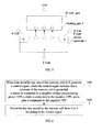
- a structure of the floating-gate MOS transistor is shown in FIG 3 , where FIG 3 is a schematic structural diagram of a floating-gate MOS transistor according to Embodiment 3 of the present invention. It can be seen from FIG 3 that, the floating-gate MOS transistor is an N-channel floating-gate MOS transistor, where a floating gate 2 is located between a metal gate 1 and a P-type silicon substrate 3. A source, a drain, and a gate of the floating-gate MOS transistor are shown in FIG 3 .
- an operation of overwriting data corresponding to a current bit of the original data is performed on a bitwise basis, where bitwise overwriting includes bitwise programming and bitwise erasing.
- bitwise overwriting includes bitwise programming and bitwise erasing.
- overwriting data corresponding to a current bit of the original data from 0 to 1 may be considered as bitwise erasing
- overwriting data corresponding to a current bit of the original data from 1 to 0 may be considered as bitwise programming.
- a first control signal is generated when the data corresponding to the current bit of the original data is 0, where the first control signal includes that the substrate of the memory cell 102 is grounded, the source is connected to the negative VPP, the drain is connected to the negative VPP, and the gate is connected to the negative VPP.
- the memory cell 102 corresponding to the current bit receives the first control signal, and implements, according to a voltage connection condition of the substrate, the source, the drain, and the gate of the memory cell in the first control signal, that the substrate is grounded, the source is connected to the negative VPP (that is, -VPP), the drain is connected to the negative VPP, and the gate is connected to the negative VPP in the floating-gate MOS transistor, as shown in FIG 4 , where FIG 4 is a schematic diagram of a floating-gate MOS transistor where 0 is overwritten into 1 according to Embodiment 3 of the present invention.
- channel field strength distribution formed thereby enables an electric charge on a floating gate to be moved to a channel, hence the electric charge on the floating gate is completely removed, thereby implementing a process of overwriting the data, which is stored by the memory cell and corresponds to the current bit, from 0 to 1. That is, a process of bitwise erasing is implemented.
- control circuit 101 is further configured to generate a second control signal if data corresponding to a current bit of the original data is inconsistent with data corresponding to a current bit of the data to be written and when the data corresponding to the current bit of the original data is 1, so that the memory cell corresponding to the current bit overwrites the data stored by the memory cell from 1 to 0, where the second control signal includes that the substrate of the memory cell is grounded, the source is grounded, the drain is grounded, and the gate is connected to a VPP.
- a second control signal is generated when the data corresponding to the current bit of the original data is 1, where the second control signal includes that the substrate of the memory cell is grounded, the source is grounded, the drain is grounded, and the gate is connected to the VPP.
- the memory cell 102 corresponding to the current bit receives the second control signal, and implements, according to a voltage connection condition of the substrate, the source, the drain, and the gate of the memory cell in the second control signal, that the substrate is grounded, the source is grounded, the drain is grounded, and the gate is connected to the voltage programming power VPP in the floating-gate MOS transistor, as shown in FIG 5 , where FIG. 5 is a schematic diagram of a floating-gate MOS transistor where 1 is overwritten into 0 provided by Embodiment 3 of the present invention.
- a control circuit of the Flash when original data in a memory cell of a Flash needs to be updated, a control circuit of the Flash reads the original data of a region to be updated; determines, on a bitwise basis, whether the original data is consistent with data to be written; and if inconsistent, generates a corresponding control signal, so that the memory cell corresponding to the current bit of the Flash overwrites the data corresponding to the current bit of the original data according to the corresponding control signal, thereby implementing bitwise erasing and bitwise programming on the data and implementing data updating.
- a corresponding overwrite operation is directly performed only on a bit to be updated, and it is unnecessary to search for a new block to write all data to be written or to perform an erase operation on a block to store data, which correspondingly reduces the times of additional read operations and write operations, thereby improving the operating efficiency and extending a service life of a Flash.
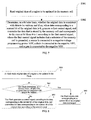
- FIG. 6 is a flowchart of a method embodiment for processing data according to Embodiment 4 of the present invention.
- the method for processing data is applicable to the Flash in Embodiment 1.
- the method for processing data includes the following steps:
- the control signal is generated, where the control signal includes that the substrate of the memory cell is grounded, the source is connected to the negative VPP, the drain is connected to the negative VPP, and the gate is connected to the negative VPP.
- the substrate is grounded, the source is connected to the negative VPP, the drain is connected to the negative VPP, and the gate is connected to the negative VPP in the floating-gate MOS transistor.
- channel field strength distribution formed thereby enables an electric charge on a floating-gate to be moved to a channel, hence the electric charge on the floating gate is completely removed, thereby implementing a process of overwriting data corresponding to a current bit from 0 to 1. That is, a process of bitwise erasing is implemented.
- a control signal is generated, and the data stored by the memory cell is overwritten from 0 to 1 according to the control signal, thereby implementing bitwise erasing on the data and implementing data updating.
- a corresponding overwrite operation is directly performed only on a bit to be updated, and it is unnecessary to search for a new block to write all data to be written or to perform an erase operation on a block to perform data storage, which correspondingly reduces the times of additional read operations and write operations, thereby improving the operating efficiency and extending a service life of a flash memory.
- FIG 7 is a flowchart of a method embodiment for processing data according to Embodiment 5 of the present invention.
- the method for processing data is applicable to the Flash in Embodiment 2 or 3.
- the method for processing data includes the following steps:
- the original data of the region to be updated is read; it is determined, on a bitwise basis, whether the original data is consistent with data to be written; and if inconsistent, when data corresponding to a current bit of the original data is 0, a first control signal is generated, so that the memory cell corresponding to the current bit overwrites data stored by the memory cell from 0 to 1, thereby implementing bitwise erasing on the data and implementing data updating.
- a corresponding overwrite operation is directly performed only on a bit to be updated, and it is unnecessary to search for a new block to write all data to be written or to perform an erase operation on a block to perform data storage, which correspondingly reduces the times of additional read operations and write operations, thereby improving the operating efficiency and extending a service life of a flash memory.
- FIG 8 is a flowchart of a method embodiment for processing data according to Embodiment 6 of the present invention.
- the method for processing data is applicable to the Flash in Embodiment 2 or 3.
- the method for processing data includes the following steps:
- the Flash includes several blocks, each block includes several pages, and each page includes several bytes.
- a width of a byte may be changed according to specific requirements, and generally is 8 bits, 16 bits, 32 bits, or the like.
- the Flash may specifically address each byte when performing addressing.
- a control circuit 101 of the Flash may read the original data of the region to be updated, where the original data may be stored in a binary form.
- the original data is 10101001.
- the control circuit 101 may read the original data on a bitwise (bit) basis.
- S602 The Flash determines, on a bitwise basis, whether the original data is consistent with data to be written; and if yes, performs S603; if inconsistent, performs S604.
- the original data After the original data is read, it is determined, on a bitwise basis, whether the original data is consistent with the data to be written.
- the data to be written is 00111001
- the data corresponding to the current bit of the original data is consistent with data corresponding to a current bit of the data to be written, such as bits 0, 1, 2, 3, 5, and 6, no operation is performed on the data corresponding to the current bit of the original data.
- the Flash generates a control signal according to the data corresponding to the current bit of the original data, and overwrites the data corresponding to the current bit of the original data according to the control signal.
- the control signal is generated according to the data corresponding to the current bit of the original data, and the control signal is sent to a memory cell 102 corresponding to the current bit, where the control signal includes a voltage connection condition of a substrate, a source, a drain, and a gate of the memory cell corresponding to the current bit.
- the generating the control signal according to the data corresponding to the current bit of the original data includes:
- the overwriting the data corresponding to the current bit of the original data according to the control signal includes:
- the substrate is grounded, the source is connected to the negative VPP, the drain is connected to the negative VPP, and the gate is connected to the negative VPP in the floating-gate MOS transistor.
- the floating-gate MOS transistor is connected in this manner, channel field strength distribution formed thereby enables an electric charge on a floating-gate to be moved to a channel, hence the electric charge on the floating gate is completely removed, thereby implementing a process of overwriting the data corresponding to the current bit from 0 to 1. That is, a process of bitwise erasing is implemented.
- the generating the control signal according to the data corresponding to the current bit of the original data includes:
- the overwriting the data corresponding to the current bit of the original data according to the control signal includes:
- the substrate is grounded, the source is grounded, the drain is grounded, and the gate is connected to the VPP in the floating-gate MOS transistor.
- the floating-gate MOS transistor is connected in this manner, charging a floating gate is performing programming on the current bit, thereby implementing a process of overwriting the data corresponding to the current bit from 1 to 0. That is, a process of bitwise programming is implemented.
- a Flash may directly address each byte on the page 1 and the page 2 of the block A when performing addressing; reads original data on the page 1 and the page 2 of the block A according to bits in the byte; separately determines, on a bitwise basis, whether the original data on the page 1 and the page 2 is consistent with the data to be written; if consistent, retains data corresponding to a current bit of the original data unchanged; and if inconsistent, generates a control signal according to the data corresponding to the current bit of the original data, and overwrites the data corresponding to the current bit of the original data according to the control signal.
- the data corresponding to the current bit of the original data may, according to the control signal, be overwritten from 1 to 0 or be overwritten from 0 to 1, thereby implementing data updating on the page 1 and the page 2 of the block A.
- storage may be performed without completely erasing a block, and an overwrite operation may be performed, on a bitwise basis, directly on a block to be updated to implement data storage.
- the original data of a region to be updated is read; it is determined, on a bitwise basis, whether the original data is consistent with data to be written; and if yes, no processing is performed on data corresponding to a current bit of the original data; and if inconsistent, a control signal is generated and the data corresponding to the current bit of the original data is overwritten according to the control signal, thereby implementing bitwise erasing and bitwise programming on the data and implementing data updating.
- a corresponding overwrite operation is directly performed only on a bit to be updated, and it is unnecessary to search for a new block to write all data to be written or to perform an erase operation on a block to perform data storage, which correspondingly reduces the times of additional read operations and write operations, and reduces time for programming data and time for reading data, thereby improving the operating efficiency and extending a service life of a Flash.
- FIG 9 is a schematic structural diagram of a terminal embodiment according to Embodiment 7 of the present invention.
- the terminal includes a flash memory 10, where the flash memory 10 includes a control circuit 101 and a plurality of memory cells 102.
- a function of the control circuit 101 is similar to a function of the control circuit 101 in Embodiment 1, Embodiment 2, or Embodiment 3, which is not described repeatedly herein. For details, refer to the related description of Embodiment 1, Embodiment 2, or Embodiment 3.
- a function of the memory cell 102 is similar to a function of the memory cell 102 in Embodiment 1, Embodiment 2, or Embodiment 3, which is not described repeatedly herein. For details, refer to the related description of Embodiment 1, Embodiment 2, or Embodiment 3.
- original data in a Flash of a terminal when original data in a Flash of a terminal needs to be updated, original data of a region to be updated may be read; it is determined, on a bitwise basis, whether the original data is consistent with data to be written; and if yes, no processing is performed on data corresponding to a current bit of the original data; if inconsistent, a control signal is generated and the data corresponding to the current bit of the original data is overwritten according to the control signal, thereby implementing bitwise erasing and bitwise programming on the data, and eventually implementing data updating.
- a corresponding overwrite operation is directly performed only on a bit to be updated, and it is unnecessary to search for a new block to write all data to be written or to perform an erase operation on a block to perform data storage, which correspondingly reduces the times of additional read operations and write operations, and reduces time for programming data and time for reading data, thereby improving the operating efficiency and extending a service life of a Flash.
- the program may be stored in a computer readable storage medium.
- the foregoing storage medium may be a read-only memory, a magnetic disk, or an optical disc.
Landscapes
- Engineering & Computer Science (AREA)
- Microelectronics & Electronic Packaging (AREA)
- Read Only Memory (AREA)
Applications Claiming Priority (1)
| Application Number | Priority Date | Filing Date | Title |
|---|---|---|---|
| PCT/CN2012/076108 WO2012126434A2 (fr) | 2012-05-25 | 2012-05-25 | Procédé de traitement de données, mémoire flash et terminal |
Publications (3)
| Publication Number | Publication Date |
|---|---|
| EP2840610A2 true EP2840610A2 (fr) | 2015-02-25 |
| EP2840610A4 EP2840610A4 (fr) | 2015-06-03 |
| EP2840610B1 EP2840610B1 (fr) | 2019-04-03 |
Family
ID=46879810
Family Applications (1)
| Application Number | Title | Priority Date | Filing Date |
|---|---|---|---|
| EP12761495.6A Not-in-force EP2840610B1 (fr) | 2012-05-25 | 2012-05-25 | Procédé de traitement de données, mémoire flash et terminal |
Country Status (4)
| Country | Link |
|---|---|
| US (1) | US9281063B2 (fr) |
| EP (1) | EP2840610B1 (fr) |
| CN (1) | CN102986029B (fr) |
| WO (1) | WO2012126434A2 (fr) |
Families Citing this family (9)
| Publication number | Priority date | Publication date | Assignee | Title |
|---|---|---|---|---|
| US10331561B1 (en) | 2016-06-29 | 2019-06-25 | Emc Corporation | Systems and methods for rebuilding a cache index |
| US10055351B1 (en) | 2016-06-29 | 2018-08-21 | EMC IP Holding Company LLC | Low-overhead index for a flash cache |
| US10089025B1 (en) | 2016-06-29 | 2018-10-02 | EMC IP Holding Company LLC | Bloom filters in a flash memory |
| US10146438B1 (en) | 2016-06-29 | 2018-12-04 | EMC IP Holding Company LLC | Additive library for data structures in a flash memory |
| US10261704B1 (en) | 2016-06-29 | 2019-04-16 | EMC IP Holding Company LLC | Linked lists in flash memory |
| US10037164B1 (en) | 2016-06-29 | 2018-07-31 | EMC IP Holding Company LLC | Flash interface for processing datasets |
| US10445008B2 (en) * | 2017-09-15 | 2019-10-15 | Macronix International Co., Ltd. | Data management method for memory and memory apparatus |
| WO2021021161A1 (fr) * | 2019-07-31 | 2021-02-04 | Hewlett-Packard Development Company, L.P. | Mises à jour d'une mémoire flash sur la base de déterminations de bits à effacer |
| US11704035B2 (en) * | 2020-03-30 | 2023-07-18 | Pure Storage, Inc. | Unified storage on block containers |
Family Cites Families (8)
| Publication number | Priority date | Publication date | Assignee | Title |
|---|---|---|---|---|
| JP2794974B2 (ja) * | 1991-04-10 | 1998-09-10 | 日本電気株式会社 | 不揮発性半導体記憶装置の起動方法 |
| US6418060B1 (en) * | 2002-01-03 | 2002-07-09 | Ememory Technology Inc. | Method of programming and erasing non-volatile memory cells |
| TW565910B (en) * | 2002-10-24 | 2003-12-11 | Amic Technology Corp | Negative voltage switch and related flash memory for transmitting negative voltage with triple-well transistors |
| US7907450B2 (en) * | 2006-05-08 | 2011-03-15 | Macronix International Co., Ltd. | Methods and apparatus for implementing bit-by-bit erase of a flash memory device |
| KR100871606B1 (ko) * | 2007-06-18 | 2008-12-02 | 삼성전자주식회사 | 비휘발성 메모리 소자의 프로그래밍 방법 및 이를 이용한낸드 플래시 메모리 소자의 구동 방법 |
| JP4881401B2 (ja) * | 2009-03-23 | 2012-02-22 | 株式会社東芝 | Nand型フラッシュメモリ |
| CN102456745B (zh) | 2010-10-22 | 2013-09-04 | 北京大学 | 一种快闪存储器及其制备方法和操作方法 |
| CN102339644B (zh) | 2011-07-27 | 2014-12-24 | 聚辰半导体(上海)有限公司 | 存储器及其操作方法 |
-
2012
- 2012-05-25 WO PCT/CN2012/076108 patent/WO2012126434A2/fr active Application Filing
- 2012-05-25 EP EP12761495.6A patent/EP2840610B1/fr not_active Not-in-force
- 2012-05-25 CN CN201280001571.6A patent/CN102986029B/zh not_active Expired - Fee Related
-
2014
- 2014-07-11 US US14/329,460 patent/US9281063B2/en not_active Expired - Fee Related
Also Published As
| Publication number | Publication date |
|---|---|
| US20140321210A1 (en) | 2014-10-30 |
| US9281063B2 (en) | 2016-03-08 |
| EP2840610A4 (fr) | 2015-06-03 |
| CN102986029B (zh) | 2015-07-22 |
| WO2012126434A3 (fr) | 2012-11-08 |
| WO2012126434A2 (fr) | 2012-09-27 |
| EP2840610B1 (fr) | 2019-04-03 |
| CN102986029A (zh) | 2013-03-20 |
Similar Documents
| Publication | Publication Date | Title |
|---|---|---|
| US9281063B2 (en) | Method for processing data, flash memory, and terminal | |
| US8255762B2 (en) | Semiconductor memory device with error correction | |
| US7248504B2 (en) | Data processing device | |
| US7313029B2 (en) | Method for erasing flash memories and related system thereof | |
| US8190810B2 (en) | Non-volatile memory apparatus and method for accessing a non-volatile memory apparatus | |
| JP2009134416A (ja) | メモリシステム | |
| KR20080097646A (ko) | 비휘발성 메모리의 멀티 비트 프로그래밍 장치 및 방법 | |
| US7248503B2 (en) | Semiconductor nonvolatile storage device | |
| US20100318729A1 (en) | Nonvolatile semiconductor memory device | |
| JP2009151920A5 (fr) | ||
| WO2015155860A1 (fr) | Dispositif de stockage d'informations et procédé de commande de dispositif de stockage d'informations | |
| US7212438B2 (en) | Semiconductor device and method of operating a semiconductor device | |
| KR20020089587A (ko) | 공유벌크로 형성된 섹터구조를 갖는 불휘발성 반도체메모리 장치 | |
| KR20180029576A (ko) | 고전압 스위치 회로 및 이를 포함하는 반도체 메모리 장치 | |
| KR20190056862A (ko) | 메모리 시스템 및 그것의 동작 방법 | |
| JP2015103093A (ja) | フラッシュメモリ、バッドブロックの管理方法および管理プログラム | |
| CN110908825B (zh) | 一种数据读取方法、装置、存储设备及存储介质 | |
| US20100302856A1 (en) | Nonvolatile memory device and method of programming and reading the same | |
| US10163499B2 (en) | Method for increasing speed of writing data into flash memory unit and associated device | |
| CN109147851B (zh) | 一种锁存电路 | |
| US9536602B2 (en) | Method for writing data into flash memory and related control apparatus | |
| US20110286281A1 (en) | Reference current generator used for programming and erasing of non-volatile memory | |
| CN110648714B (zh) | 数据的读取方法、装置、电子设备和存储介质 | |
| JP5260152B2 (ja) | 不揮発性メモリ制御回路 | |
| KR20160099455A (ko) | 메모리 동작용 시스템, 디바이스 및 방법 |
Legal Events
| Date | Code | Title | Description |
|---|---|---|---|
| PUAI | Public reference made under article 153(3) epc to a published international application that has entered the european phase |
Free format text: ORIGINAL CODE: 0009012 |
|
| 17P | Request for examination filed |
Effective date: 20140625 |
|
| AK | Designated contracting states |
Kind code of ref document: A2 Designated state(s): AL AT BE BG CH CY CZ DE DK EE ES FI FR GB GR HR HU IE IS IT LI LT LU LV MC MK MT NL NO PL PT RO RS SE SI SK SM TR |
|
| AX | Request for extension of the european patent |
Extension state: BA ME |
|
| A4 | Supplementary search report drawn up and despatched |
Effective date: 20150508 |
|
| RIC1 | Information provided on ipc code assigned before grant |
Ipc: G11C 16/04 20060101ALI20150430BHEP Ipc: H01L 27/115 20060101AFI20150430BHEP Ipc: G11C 16/06 20060101ALI20150430BHEP Ipc: G11C 16/16 20060101ALI20150430BHEP |
|
| DAX | Request for extension of the european patent (deleted) | ||
| GRAP | Despatch of communication of intention to grant a patent |
Free format text: ORIGINAL CODE: EPIDOSNIGR1 |
|
| STAA | Information on the status of an ep patent application or granted ep patent |
Free format text: STATUS: GRANT OF PATENT IS INTENDED |
|
| INTG | Intention to grant announced |
Effective date: 20181024 |
|
| GRAS | Grant fee paid |
Free format text: ORIGINAL CODE: EPIDOSNIGR3 |
|
| GRAA | (expected) grant |
Free format text: ORIGINAL CODE: 0009210 |
|
| STAA | Information on the status of an ep patent application or granted ep patent |
Free format text: STATUS: THE PATENT HAS BEEN GRANTED |
|
| AK | Designated contracting states |
Kind code of ref document: B1 Designated state(s): AL AT BE BG CH CY CZ DE DK EE ES FI FR GB GR HR HU IE IS IT LI LT LU LV MC MK MT NL NO PL PT RO RS SE SI SK SM TR |
|
| REG | Reference to a national code |
Ref country code: GB Ref legal event code: FG4D |
|
| REG | Reference to a national code |
Ref country code: CH Ref legal event code: EP Ref country code: AT Ref legal event code: REF Ref document number: 1116781 Country of ref document: AT Kind code of ref document: T Effective date: 20190415 |
|
| REG | Reference to a national code |
Ref country code: DE Ref legal event code: R096 Ref document number: 602012058593 Country of ref document: DE |
|
| REG | Reference to a national code |
Ref country code: IE Ref legal event code: FG4D |
|
| REG | Reference to a national code |
Ref country code: NL Ref legal event code: MP Effective date: 20190403 |
|
| REG | Reference to a national code |
Ref country code: LT Ref legal event code: MG4D |
|
| REG | Reference to a national code |
Ref country code: AT Ref legal event code: MK05 Ref document number: 1116781 Country of ref document: AT Kind code of ref document: T Effective date: 20190403 |
|
| PG25 | Lapsed in a contracting state [announced via postgrant information from national office to epo] |
Ref country code: NL Free format text: LAPSE BECAUSE OF FAILURE TO SUBMIT A TRANSLATION OF THE DESCRIPTION OR TO PAY THE FEE WITHIN THE PRESCRIBED TIME-LIMIT Effective date: 20190403 |
|
| PG25 | Lapsed in a contracting state [announced via postgrant information from national office to epo] |
Ref country code: ES Free format text: LAPSE BECAUSE OF FAILURE TO SUBMIT A TRANSLATION OF THE DESCRIPTION OR TO PAY THE FEE WITHIN THE PRESCRIBED TIME-LIMIT Effective date: 20190403 Ref country code: SE Free format text: LAPSE BECAUSE OF FAILURE TO SUBMIT A TRANSLATION OF THE DESCRIPTION OR TO PAY THE FEE WITHIN THE PRESCRIBED TIME-LIMIT Effective date: 20190403 Ref country code: PT Free format text: LAPSE BECAUSE OF FAILURE TO SUBMIT A TRANSLATION OF THE DESCRIPTION OR TO PAY THE FEE WITHIN THE PRESCRIBED TIME-LIMIT Effective date: 20190803 Ref country code: AL Free format text: LAPSE BECAUSE OF FAILURE TO SUBMIT A TRANSLATION OF THE DESCRIPTION OR TO PAY THE FEE WITHIN THE PRESCRIBED TIME-LIMIT Effective date: 20190403 Ref country code: CZ Free format text: LAPSE BECAUSE OF FAILURE TO SUBMIT A TRANSLATION OF THE DESCRIPTION OR TO PAY THE FEE WITHIN THE PRESCRIBED TIME-LIMIT Effective date: 20190403 Ref country code: HR Free format text: LAPSE BECAUSE OF FAILURE TO SUBMIT A TRANSLATION OF THE DESCRIPTION OR TO PAY THE FEE WITHIN THE PRESCRIBED TIME-LIMIT Effective date: 20190403 Ref country code: LT Free format text: LAPSE BECAUSE OF FAILURE TO SUBMIT A TRANSLATION OF THE DESCRIPTION OR TO PAY THE FEE WITHIN THE PRESCRIBED TIME-LIMIT Effective date: 20190403 Ref country code: NO Free format text: LAPSE BECAUSE OF FAILURE TO SUBMIT A TRANSLATION OF THE DESCRIPTION OR TO PAY THE FEE WITHIN THE PRESCRIBED TIME-LIMIT Effective date: 20190703 Ref country code: FI Free format text: LAPSE BECAUSE OF FAILURE TO SUBMIT A TRANSLATION OF THE DESCRIPTION OR TO PAY THE FEE WITHIN THE PRESCRIBED TIME-LIMIT Effective date: 20190403 |
|
| PG25 | Lapsed in a contracting state [announced via postgrant information from national office to epo] |
Ref country code: RS Free format text: LAPSE BECAUSE OF FAILURE TO SUBMIT A TRANSLATION OF THE DESCRIPTION OR TO PAY THE FEE WITHIN THE PRESCRIBED TIME-LIMIT Effective date: 20190403 Ref country code: PL Free format text: LAPSE BECAUSE OF FAILURE TO SUBMIT A TRANSLATION OF THE DESCRIPTION OR TO PAY THE FEE WITHIN THE PRESCRIBED TIME-LIMIT Effective date: 20190403 Ref country code: GR Free format text: LAPSE BECAUSE OF FAILURE TO SUBMIT A TRANSLATION OF THE DESCRIPTION OR TO PAY THE FEE WITHIN THE PRESCRIBED TIME-LIMIT Effective date: 20190704 Ref country code: BG Free format text: LAPSE BECAUSE OF FAILURE TO SUBMIT A TRANSLATION OF THE DESCRIPTION OR TO PAY THE FEE WITHIN THE PRESCRIBED TIME-LIMIT Effective date: 20190703 Ref country code: LV Free format text: LAPSE BECAUSE OF FAILURE TO SUBMIT A TRANSLATION OF THE DESCRIPTION OR TO PAY THE FEE WITHIN THE PRESCRIBED TIME-LIMIT Effective date: 20190403 |
|
| REG | Reference to a national code |
Ref country code: CH Ref legal event code: PL |
|
| PG25 | Lapsed in a contracting state [announced via postgrant information from national office to epo] |
Ref country code: IS Free format text: LAPSE BECAUSE OF FAILURE TO SUBMIT A TRANSLATION OF THE DESCRIPTION OR TO PAY THE FEE WITHIN THE PRESCRIBED TIME-LIMIT Effective date: 20190803 Ref country code: AT Free format text: LAPSE BECAUSE OF FAILURE TO SUBMIT A TRANSLATION OF THE DESCRIPTION OR TO PAY THE FEE WITHIN THE PRESCRIBED TIME-LIMIT Effective date: 20190403 |
|
| REG | Reference to a national code |
Ref country code: DE Ref legal event code: R097 Ref document number: 602012058593 Country of ref document: DE |
|
| PG25 | Lapsed in a contracting state [announced via postgrant information from national office to epo] |
Ref country code: LI Free format text: LAPSE BECAUSE OF NON-PAYMENT OF DUE FEES Effective date: 20190531 Ref country code: DK Free format text: LAPSE BECAUSE OF FAILURE TO SUBMIT A TRANSLATION OF THE DESCRIPTION OR TO PAY THE FEE WITHIN THE PRESCRIBED TIME-LIMIT Effective date: 20190403 Ref country code: CH Free format text: LAPSE BECAUSE OF NON-PAYMENT OF DUE FEES Effective date: 20190531 Ref country code: MC Free format text: LAPSE BECAUSE OF FAILURE TO SUBMIT A TRANSLATION OF THE DESCRIPTION OR TO PAY THE FEE WITHIN THE PRESCRIBED TIME-LIMIT Effective date: 20190403 Ref country code: SK Free format text: LAPSE BECAUSE OF FAILURE TO SUBMIT A TRANSLATION OF THE DESCRIPTION OR TO PAY THE FEE WITHIN THE PRESCRIBED TIME-LIMIT Effective date: 20190403 Ref country code: EE Free format text: LAPSE BECAUSE OF FAILURE TO SUBMIT A TRANSLATION OF THE DESCRIPTION OR TO PAY THE FEE WITHIN THE PRESCRIBED TIME-LIMIT Effective date: 20190403 Ref country code: RO Free format text: LAPSE BECAUSE OF FAILURE TO SUBMIT A TRANSLATION OF THE DESCRIPTION OR TO PAY THE FEE WITHIN THE PRESCRIBED TIME-LIMIT Effective date: 20190403 |
|
| REG | Reference to a national code |
Ref country code: BE Ref legal event code: MM Effective date: 20190531 |
|
| PLBE | No opposition filed within time limit |
Free format text: ORIGINAL CODE: 0009261 |
|
| STAA | Information on the status of an ep patent application or granted ep patent |
Free format text: STATUS: NO OPPOSITION FILED WITHIN TIME LIMIT |
|
| PG25 | Lapsed in a contracting state [announced via postgrant information from national office to epo] |
Ref country code: LU Free format text: LAPSE BECAUSE OF NON-PAYMENT OF DUE FEES Effective date: 20190525 Ref country code: SM Free format text: LAPSE BECAUSE OF FAILURE TO SUBMIT A TRANSLATION OF THE DESCRIPTION OR TO PAY THE FEE WITHIN THE PRESCRIBED TIME-LIMIT Effective date: 20190403 Ref country code: IT Free format text: LAPSE BECAUSE OF FAILURE TO SUBMIT A TRANSLATION OF THE DESCRIPTION OR TO PAY THE FEE WITHIN THE PRESCRIBED TIME-LIMIT Effective date: 20190403 |
|
| 26N | No opposition filed |
Effective date: 20200106 |
|
| PG25 | Lapsed in a contracting state [announced via postgrant information from national office to epo] |
Ref country code: TR Free format text: LAPSE BECAUSE OF FAILURE TO SUBMIT A TRANSLATION OF THE DESCRIPTION OR TO PAY THE FEE WITHIN THE PRESCRIBED TIME-LIMIT Effective date: 20190403 |
|
| PG25 | Lapsed in a contracting state [announced via postgrant information from national office to epo] |
Ref country code: IE Free format text: LAPSE BECAUSE OF NON-PAYMENT OF DUE FEES Effective date: 20190525 |
|
| PG25 | Lapsed in a contracting state [announced via postgrant information from national office to epo] |
Ref country code: BE Free format text: LAPSE BECAUSE OF NON-PAYMENT OF DUE FEES Effective date: 20190531 Ref country code: SI Free format text: LAPSE BECAUSE OF FAILURE TO SUBMIT A TRANSLATION OF THE DESCRIPTION OR TO PAY THE FEE WITHIN THE PRESCRIBED TIME-LIMIT Effective date: 20190403 |
|
| PG25 | Lapsed in a contracting state [announced via postgrant information from national office to epo] |
Ref country code: CY Free format text: LAPSE BECAUSE OF FAILURE TO SUBMIT A TRANSLATION OF THE DESCRIPTION OR TO PAY THE FEE WITHIN THE PRESCRIBED TIME-LIMIT Effective date: 20190403 |
|
| PG25 | Lapsed in a contracting state [announced via postgrant information from national office to epo] |
Ref country code: HU Free format text: LAPSE BECAUSE OF FAILURE TO SUBMIT A TRANSLATION OF THE DESCRIPTION OR TO PAY THE FEE WITHIN THE PRESCRIBED TIME-LIMIT; INVALID AB INITIO Effective date: 20120525 Ref country code: MT Free format text: LAPSE BECAUSE OF FAILURE TO SUBMIT A TRANSLATION OF THE DESCRIPTION OR TO PAY THE FEE WITHIN THE PRESCRIBED TIME-LIMIT Effective date: 20190403 |
|
| PGFP | Annual fee paid to national office [announced via postgrant information from national office to epo] |
Ref country code: DE Payment date: 20210427 Year of fee payment: 10 Ref country code: FR Payment date: 20210412 Year of fee payment: 10 |
|
| PGFP | Annual fee paid to national office [announced via postgrant information from national office to epo] |
Ref country code: GB Payment date: 20210428 Year of fee payment: 10 |
|
| PG25 | Lapsed in a contracting state [announced via postgrant information from national office to epo] |
Ref country code: MK Free format text: LAPSE BECAUSE OF FAILURE TO SUBMIT A TRANSLATION OF THE DESCRIPTION OR TO PAY THE FEE WITHIN THE PRESCRIBED TIME-LIMIT Effective date: 20190403 |
|
| REG | Reference to a national code |
Ref country code: DE Ref legal event code: R079 Ref document number: 602012058593 Country of ref document: DE Free format text: PREVIOUS MAIN CLASS: H01L0027115000 Ipc: H10B0069000000 |
|
| REG | Reference to a national code |
Ref country code: DE Ref legal event code: R119 Ref document number: 602012058593 Country of ref document: DE |
|
| GBPC | Gb: european patent ceased through non-payment of renewal fee |
Effective date: 20220525 |
|
| PG25 | Lapsed in a contracting state [announced via postgrant information from national office to epo] |
Ref country code: FR Free format text: LAPSE BECAUSE OF NON-PAYMENT OF DUE FEES Effective date: 20220531 |
|
| PG25 | Lapsed in a contracting state [announced via postgrant information from national office to epo] |
Ref country code: GB Free format text: LAPSE BECAUSE OF NON-PAYMENT OF DUE FEES Effective date: 20220525 Ref country code: DE Free format text: LAPSE BECAUSE OF NON-PAYMENT OF DUE FEES Effective date: 20221201 |