EP2837642A2 - Lichthärtbare Zusammensetzung und damit hergestellte eingekapselte Vorrichtung - Google Patents
Lichthärtbare Zusammensetzung und damit hergestellte eingekapselte Vorrichtung Download PDFInfo
- Publication number
- EP2837642A2 EP2837642A2 EP14177801.9A EP14177801A EP2837642A2 EP 2837642 A2 EP2837642 A2 EP 2837642A2 EP 14177801 A EP14177801 A EP 14177801A EP 2837642 A2 EP2837642 A2 EP 2837642A2
- Authority
- EP
- European Patent Office
- Prior art keywords
- photocurable composition
- photocurable
- group
- substituted
- unsubstituted
- Prior art date
- Legal status (The legal status is an assumption and is not a legal conclusion. Google has not performed a legal analysis and makes no representation as to the accuracy of the status listed.)
- Granted
Links
Images

Classifications
-
- C—CHEMISTRY; METALLURGY
- C08—ORGANIC MACROMOLECULAR COMPOUNDS; THEIR PREPARATION OR CHEMICAL WORKING-UP; COMPOSITIONS BASED THEREON
- C08F—MACROMOLECULAR COMPOUNDS OBTAINED BY REACTIONS ONLY INVOLVING CARBON-TO-CARBON UNSATURATED BONDS
- C08F2/00—Processes of polymerisation
- C08F2/46—Polymerisation initiated by wave energy or particle radiation
- C08F2/48—Polymerisation initiated by wave energy or particle radiation by ultraviolet or visible light
-
- C—CHEMISTRY; METALLURGY
- C08—ORGANIC MACROMOLECULAR COMPOUNDS; THEIR PREPARATION OR CHEMICAL WORKING-UP; COMPOSITIONS BASED THEREON
- C08F—MACROMOLECULAR COMPOUNDS OBTAINED BY REACTIONS ONLY INVOLVING CARBON-TO-CARBON UNSATURATED BONDS
- C08F222/00—Copolymers of compounds having one or more unsaturated aliphatic radicals, each having only one carbon-to-carbon double bond, and at least one being terminated by a carboxyl radical and containing at least one other carboxyl radical in the molecule; Salts, anhydrides, esters, amides, imides, or nitriles thereof
- C08F222/10—Esters
- C08F222/1006—Esters of polyhydric alcohols or polyhydric phenols
- C08F222/102—Esters of polyhydric alcohols or polyhydric phenols of dialcohols, e.g. ethylene glycol di(meth)acrylate or 1,4-butanediol dimethacrylate
-
- C—CHEMISTRY; METALLURGY
- C08—ORGANIC MACROMOLECULAR COMPOUNDS; THEIR PREPARATION OR CHEMICAL WORKING-UP; COMPOSITIONS BASED THEREON
- C08F—MACROMOLECULAR COMPOUNDS OBTAINED BY REACTIONS ONLY INVOLVING CARBON-TO-CARBON UNSATURATED BONDS
- C08F2/00—Processes of polymerisation
- C08F2/46—Polymerisation initiated by wave energy or particle radiation
- C08F2/48—Polymerisation initiated by wave energy or particle radiation by ultraviolet or visible light
- C08F2/50—Polymerisation initiated by wave energy or particle radiation by ultraviolet or visible light with sensitising agents
-
- C—CHEMISTRY; METALLURGY
- C08—ORGANIC MACROMOLECULAR COMPOUNDS; THEIR PREPARATION OR CHEMICAL WORKING-UP; COMPOSITIONS BASED THEREON
- C08F—MACROMOLECULAR COMPOUNDS OBTAINED BY REACTIONS ONLY INVOLVING CARBON-TO-CARBON UNSATURATED BONDS
- C08F220/00—Copolymers of compounds having one or more unsaturated aliphatic radicals, each having only one carbon-to-carbon double bond, and only one being terminated by only one carboxyl radical or a salt, anhydride ester, amide, imide or nitrile thereof
- C08F220/02—Monocarboxylic acids having less than ten carbon atoms; Derivatives thereof
- C08F220/10—Esters
- C08F220/12—Esters of monohydric alcohols or phenols
- C08F220/16—Esters of monohydric alcohols or phenols of phenols or of alcohols containing two or more carbon atoms
- C08F220/18—Esters of monohydric alcohols or phenols of phenols or of alcohols containing two or more carbon atoms with acrylic or methacrylic acids
-
- C—CHEMISTRY; METALLURGY
- C08—ORGANIC MACROMOLECULAR COMPOUNDS; THEIR PREPARATION OR CHEMICAL WORKING-UP; COMPOSITIONS BASED THEREON
- C08F—MACROMOLECULAR COMPOUNDS OBTAINED BY REACTIONS ONLY INVOLVING CARBON-TO-CARBON UNSATURATED BONDS
- C08F230/00—Copolymers of compounds having one or more unsaturated aliphatic radicals, each having only one carbon-to-carbon double bond, and containing phosphorus, selenium, tellurium or a metal
- C08F230/02—Copolymers of compounds having one or more unsaturated aliphatic radicals, each having only one carbon-to-carbon double bond, and containing phosphorus, selenium, tellurium or a metal containing phosphorus
-
- C—CHEMISTRY; METALLURGY
- C08—ORGANIC MACROMOLECULAR COMPOUNDS; THEIR PREPARATION OR CHEMICAL WORKING-UP; COMPOSITIONS BASED THEREON
- C08F—MACROMOLECULAR COMPOUNDS OBTAINED BY REACTIONS ONLY INVOLVING CARBON-TO-CARBON UNSATURATED BONDS
- C08F230/00—Copolymers of compounds having one or more unsaturated aliphatic radicals, each having only one carbon-to-carbon double bond, and containing phosphorus, selenium, tellurium or a metal
- C08F230/04—Copolymers of compounds having one or more unsaturated aliphatic radicals, each having only one carbon-to-carbon double bond, and containing phosphorus, selenium, tellurium or a metal containing a metal
- C08F230/08—Copolymers of compounds having one or more unsaturated aliphatic radicals, each having only one carbon-to-carbon double bond, and containing phosphorus, selenium, tellurium or a metal containing a metal containing silicon
- C08F230/085—Copolymers of compounds having one or more unsaturated aliphatic radicals, each having only one carbon-to-carbon double bond, and containing phosphorus, selenium, tellurium or a metal containing a metal containing silicon the monomer being a polymerisable silane, e.g. (meth)acryloyloxy trialkoxy silanes or vinyl trialkoxysilanes
-
- H—ELECTRICITY
- H10—SEMICONDUCTOR DEVICES; ELECTRIC SOLID-STATE DEVICES NOT OTHERWISE PROVIDED FOR
- H10K—ORGANIC ELECTRIC SOLID-STATE DEVICES
- H10K50/00—Organic light-emitting devices
- H10K50/80—Constructional details
- H10K50/84—Passivation; Containers; Encapsulations
- H10K50/844—Encapsulations
-
- H—ELECTRICITY
- H10—SEMICONDUCTOR DEVICES; ELECTRIC SOLID-STATE DEVICES NOT OTHERWISE PROVIDED FOR
- H10K—ORGANIC ELECTRIC SOLID-STATE DEVICES
- H10K50/00—Organic light-emitting devices
- H10K50/80—Constructional details
- H10K50/84—Passivation; Containers; Encapsulations
- H10K50/844—Encapsulations
- H10K50/8445—Encapsulations multilayered coatings having a repetitive structure, e.g. having multiple organic-inorganic bilayers
-
- H—ELECTRICITY
- H10—SEMICONDUCTOR DEVICES; ELECTRIC SOLID-STATE DEVICES NOT OTHERWISE PROVIDED FOR
- H10K—ORGANIC ELECTRIC SOLID-STATE DEVICES
- H10K59/00—Integrated devices, or assemblies of multiple devices, comprising at least one organic light-emitting element covered by group H10K50/00
- H10K59/80—Constructional details
- H10K59/87—Passivation; Containers; Encapsulations
- H10K59/873—Encapsulations
- H10K59/8731—Encapsulations multilayered coatings having a repetitive structure, e.g. having multiple organic-inorganic bilayers
-
- H—ELECTRICITY
- H10—SEMICONDUCTOR DEVICES; ELECTRIC SOLID-STATE DEVICES NOT OTHERWISE PROVIDED FOR
- H10K—ORGANIC ELECTRIC SOLID-STATE DEVICES
- H10K85/00—Organic materials used in the body or electrodes of devices covered by this subclass
- H10K85/10—Organic polymers or oligomers
- H10K85/151—Copolymers
-
- H—ELECTRICITY
- H10—SEMICONDUCTOR DEVICES; ELECTRIC SOLID-STATE DEVICES NOT OTHERWISE PROVIDED FOR
- H10H—INORGANIC LIGHT-EMITTING SEMICONDUCTOR DEVICES HAVING POTENTIAL BARRIERS
- H10H20/00—Individual inorganic light-emitting semiconductor devices having potential barriers, e.g. light-emitting diodes [LED]
- H10H20/80—Constructional details
- H10H20/85—Packages
- H10H20/852—Encapsulations
- H10H20/854—Encapsulations characterised by their material, e.g. epoxy or silicone resins
-
- H—ELECTRICITY
- H10—SEMICONDUCTOR DEVICES; ELECTRIC SOLID-STATE DEVICES NOT OTHERWISE PROVIDED FOR
- H10K—ORGANIC ELECTRIC SOLID-STATE DEVICES
- H10K50/00—Organic light-emitting devices
- H10K50/80—Constructional details
- H10K50/84—Passivation; Containers; Encapsulations
-
- Y—GENERAL TAGGING OF NEW TECHNOLOGICAL DEVELOPMENTS; GENERAL TAGGING OF CROSS-SECTIONAL TECHNOLOGIES SPANNING OVER SEVERAL SECTIONS OF THE IPC; TECHNICAL SUBJECTS COVERED BY FORMER USPC CROSS-REFERENCE ART COLLECTIONS [XRACs] AND DIGESTS
- Y02—TECHNOLOGIES OR APPLICATIONS FOR MITIGATION OR ADAPTATION AGAINST CLIMATE CHANGE
- Y02E—REDUCTION OF GREENHOUSE GAS [GHG] EMISSIONS, RELATED TO ENERGY GENERATION, TRANSMISSION OR DISTRIBUTION
- Y02E10/00—Energy generation through renewable energy sources
- Y02E10/50—Photovoltaic [PV] energy
- Y02E10/549—Organic PV cells
Definitions
- the present invention relates to a photocurable composition and an encapsulated apparatus prepared using the same.
- An organic light emitting diode has a structure in which a functional organic layer is interposed between an anode and a cathode, and a high-energy exciton is created by recombination of holes injected into the cathode and electrons injected into the anode. The created exciton moves back to a ground state, thereby emitting light within a specific wavelength band.
- Organic light emitting diodes have merits such as self-luminescence, rapid response time, wide viewing angle, ultra-thin thickness, high image quality, and durability.
- organic light emitting diodes have problems such as deterioration in performance and lifespan thereof, causing by oxidation of organic materials and/or electrode materials due to moisture or oxygen from outside or due to outgassing inside or outside the light emitting diodes.
- some methods have been proposed, such as coating with a photocurable sealing agent, attachment of a transparent or opaque moisture absorbent, provision of frits to a substrate, on which an organic light emitting part is formed, and the like.
- Korean Patent Publication No. 2005-0021054A discloses an organic electroluminescent device and a manufacturing method thereof.
- a photocurable composition has A/B of 0.7 kgf/% or more and A of 2.5 kgf or more, when A indicates glass-metal alloy die shear strength (unit: kgf) after curing between a glass substrate and a Ni/Fe alloy and B indicates curing shrinkage (unit: %) represented by Equation 1.
- the die shear strength can be - and according to a preferred embodiment of the present invention is - measured using the method employed under 3. in the experimental section (p. 21).
- the curing shrinkage can be - and according to a preferred embodiment of the present invention is - measured using the method employed under 4. in the experimental section (p. 21).
- a composition for encapsulation of an organic light emitting diode may include the photocurable composition set forth above.
- an encapsulated apparatus may include: a member for the apparatus; and a barrier stack formed on the member for the apparatus and including an inorganic barrier layer and an organic barrier layer formed of the photocurable composition set forth above.
- hetero means that a carbon atom is substituted with an atom selected from the group consisting of N, O, S and P.
- symbol “*” as used herein means a binding site of an element.
- (meth)acrylate refers to acrylates and/or methacrylates.
- a photocurable composition has A/B of 0.7 kgf/% or more and A of 2.5 kgf or more.
- Curing shrinkage Specific gravity of solid photocurable composition after curing - Specific gravity of liquid photocurable composition before curing / Specific gravity of liquid photocurable composition before curing ⁇ 100
- the photocurable composition is deposited between the member and an inorganic barrier layer, and then cured.
- the present invention is based on the principle that, when the photocurable composition has a specific range of a ratio of adhesive strength (the strength between a glass substrate and a Ni/Fe alloy) to curing shrinkage and a specific range of adhesive strength between the glass and the Ni/Fe alloy, the encapsulated apparatus may exhibit improved reliability.
- "reliability" is determined by evaluating whether the apparatus encapsulated with the photocurable composition may be driven, after the encapsulated apparatus is left alone at 85°C and 85% RH for 500 hours.
- A/B is less than 0.7 kgf/%, when left alone at 85°C and 85% RH for 500 hours, the apparatus encapsulated with the photocurable composition is not operated well, suffering from deterioration in reliability, and may suffer from deterioration in lifespan due to severe damage to the member for the apparatus. If A is less than 2.5 kgf, when left alone at 85°C and 85% RH for 500 hours, the apparatus encapsulated with the photocurable composition is not operated well, suffering from deterioration in reliability, and may suffer from deterioration in lifespan due to severe damage to the member for the apparatus.
- the photocurable composition according to the present invention may have A/B from 1.0 kgf/% or higher, preferably 1.1 kgf/% or higher to 2 kgf/% or lower, preferably 1.5 kgf/% or lower.
- A is from 2.5 kgf or higher, preferably 5 kgf or higher, most preferred 9 kgf or higher to 15 kgf or lower, preferably 11 kgf or lower.
- Specific gravity of the liquid photocurable composition before curing and specific gravity of the solid photocurable composition obtained after curing under curing conditions of irradiation at a radiant exposure of 1000 mJ/cm 2 for 10 seconds using a light source at a wavelength of 375 nm are measured using an electronic gravimeter (DME-220E, Shinko Co., Ltd., Japan) to calculate curing shrinkage according to Equation 1.
- the photocurable composition is coated to a thickness of 10 ⁇ m ⁇ 2 ⁇ m, followed by curing, thereby preparing a film having a thickness from 8 ⁇ m to 12 ⁇ m, a width from 1.5 cm to 2.5 cm and a length from 1.5 cm to 2.5 cm. Next, specific gravity is measured on the prepared film.
- adhesive strength of a cured product of the photocurable composition formed between the Ni/Fe alloy and the glass substrate is measured.
- adhesive strength refers to strength at which a glass substrate and an 42% by weight (wt%) nickel-containing Ni/Fe alloy (about 42 wt% of Ni+about 58 wt% of Fe) are bonded to each other.
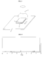
- FIG. 3 shows a final specimen for measurement of adhesive strength, and a mimetic diagram of measurement of adhesive strength using the final specimen. Referring to FIG.
- the photocurable composition is coated to a thickness of 10 ⁇ m onto a lower side of a glass substrate 1 having a size of 5 mm ⁇ 5 mm ⁇ 2 mm (width ⁇ length ⁇ height).
- a 42 wt% Ni-containing Ni/Fe alloy substrate 2 having a size of 20 mm ⁇ 80 mm ⁇ 2 mm (width ⁇ length ⁇ height) was stacked on a lower side of the photocurable composition coating layer, followed by exposure to light at a radiant exposure of 1000 mJ/cm 2 for 10 seconds using a light source at a wavelength of 375 nm.
- a specimen including a cured product 3 of the photocurable composition between the glass substrate 1 and the 42 wt% Ni-containing Ni/Fe alloy substrate 2 was prepared.
- the adhesive strength(e.g., shear die strength) was measured on the specimen using a Dage 4000 bond tester (Nordson Co., Ltd.). Referring to FIG. 3 , a die contact tool 4 of the Dage 4000 bond tester, load against and contact with the edge of the glass substrate 1 and the cured product 3 of the specimen. A contact angle between the die contact tool 4 and the edge of the specimen is almost perpendicular to the plane of the specimen.
- the adhesive strength(e.g., shear die strength) based on a measure of force applied to the specimen by the die contact tool 4. A direction of the applied force is parallel with the plane of specimen.
- the photocurable composition may include: (A1) a photocurable monomer containing phosphorus (P) and silicon (hereinafter, referred to as (A1) a photocurable monomer); (A2) a photocurable monomer, which is free from phosphorus (P) and silicon and contains an aromatic group (hereinafter, referred to as (A2) a photocurable monomer); and (A3) a photocurable monomer free from phosphorus (P), silicon and an aromatic group (hereinafter, referred to as (A3) a photocurable monomer).
- the (A1) photocurable monomer may be included in the photocurable composition.
- the photocurable composition may exhibit improved adhesive strength to the inorganic barrier layer and exhibit reduced curing shrinkage after curing, and the encapsulated apparatus may exhibit improved reliability.
- the (A1) photocurable monomer may include a vinyl group or a (meth)acrylate group as a photocurable functional group.
- the (A1) photocurable monomer may be represented by Formula 1:
- X 1 and X 2 may be each independently oxygen; R 1 may be a C 6 to C 10 aryl group or a C 7 to C 15 arylalkyl group; R 2 , R 3 , R 4 and R 5 may be each independently a C 1 to C 5 alkyl group; and R 6 may be a C 1 to C 10 alkylene group.
- the monomer represented by Formula 1 may be prepared by any typical method.
- the monomer represented by Formula 1 may be prepared by reacting a (meth)acryloyl halide with a compound represented by Formula 3: wherein Formula 3, X 1 , X 2 , R 1 , R 2 , R 3 , R 4 and R 5 are defined as in Formula 1; R 8 and R 9 are hydrogen, a substituted or unsubstituted C 1 to C 10 alkyl group, a substituted or unsubstituted C 6 to C 20 aryl group, a substituted or unsubstituted C 3 to C 10 cycloalkyl group, a substituted or unsubstituted C 7 to C 21 arylalkyl group, or -R 6 -OH; R 6 is defined as in Formula 2; and at least one of R 8 and R 9 is -R 6 -OH.
- Reaction of the compound represented by Formula 3 with the (meth)acryloyl halide may be performed at 0°C to 20°C in the presence of an organic solvent (for example, methylene chloride) and a basic compound (for example, triethylamine), without being limited thereto.
- the compound represented by Formula 3 may be prepared by any typical method.
- the compound in which both R 8 and R 9 are -R 6 -OH in Formula 3 may be prepared by reacting an unsaturated alcohol having a terminal double bond (for example, allyl alcohol) with a compound represented by Formula 4: wherein Formula 4, X 1 , X 2 , R 1 , R 2 , R 3 , R 4 and R 5 are defined as in Formula 1.
- the (A1) photocurable monomer may be present in an amount of 1 wt% or larger to 50 wt% or less, for example, 4 wt% or larger to 30 wt% or less, in the photocurable composition in terms of solid content.
- the above ranges of A/B and A may be achieved and the encapsulated apparatus does not suffer from deterioration in reliability upon encapsulation.
- the (A1) photocurable monomer may be present in an amount of 1 wt% or larger to 50 wt% or less, for example, 5 wt% or larger to 30 wt% or less, based on the total weight of the (A1)+(A2)+(A3) photocurable monomers.
- the above ranges of A/B and A may be achieved and the encapsulated apparatus does not suffer from deterioration in reliability upon encapsulation.
- the (A2) photocurable monomer is a non-phosphorus and non-silicon monomer, which is free from phosphorus (P) and silicon, has an aromatic group, and includes a vinyl group or a (meth)acrylate group as a photocurable functional group.
- the (A2) photocurable monomer may be represented by Formula 5:
- R 10 is hydrogen or a methyl group
- R 11 is a substituted or unsubstituted C 1 to C 10 aliphatic hydrocarbon group
- R 12 is a substituted or unsubstituted C 6 to C 40 aromatic hydrocarbon group.
- R 11 may be a C 1 to C 10 alkylene group or a C 3 to C 10 cycloalkylene group
- R 12 may be a C 6 to C 20 aryl group, or a C 1 to C 10 alkyl group-substituted or C 6 to C 20 aryl group-substituted C 6 to C 20 aryl group.
- the (A2) photocurable monomer may be prepared by any typical method, or may be commercially available.
- the (A2) photocurable monomer may be present in an amount of 1 wt% or larger to 50 wt% or less, for example, 5 wt% or larger to 20 wt% or less in the photocurable composition in terms of solid content.
- the above ranges of A/B and A may be achieved and the encapsulated apparatus does not suffer from deterioration in reliability upon encapsulation.
- the (A2) photocurable monomer may be present in an amount of 1 wt% or larger to 50 wt% or less, for example, 10 wt% or larger to 20 wt% or less based on the total weight of (A1)+(A2)+(A3) photocurable monomers.
- the above ranges of A/B and A may be achieved and the encapsulated apparatus does not suffer from deterioration in reliability upon encapsulation.
- the (A3) photocurable monomer is a non-phosphorus, non-silicon and nonaromatic monomer, which is free from phosphorus (P), silicon and an aromatic group, and may include a vinyl group or a (meth)acrylate group as a photocurable functional group.
- the (A3) photocurable monomer may include a mixture of a monofunctional monomer and a polyfunctional monomer.
- the monofunctional monomer and the polyfunctional monomer may be present in a weight ratio from 1:0.1 or larger to 1:4 or less, for example, from 1:1 to 1:4 or larger or less, for example, from 1:2 or larger to 1:4 or less.
- the (A3) photocurable monomer may include: unsaturated carboxylic acid esters containing a C 1 to C 20 alkyl group, a C 3 to C 20 cycloalkyl group, or a hydroxyl group; C 1 to C 20 aminoalkyl group-containing unsaturated carboxylic acid esters; vinyl esters of C 1 to C 20 saturated or unsaturated carboxylic acids; vinyl cyanide compounds; unsaturated amide compounds; monofunctional or polyfunctional (meth)acrylates of monohydric or polyhydric alcohols, or the like.
- polyhydric alcohol refers to alcohols containing two or more hydroxyl groups, for example, polyhydric alcohol containing 2 to 20 hydroxyl groups, 2 to 10 hydroxyl groups, or 2 to 6 hydroxyl groups.
- the (A3) photocurable monomer may include: unsaturated carboxylic acid esters including (meth)acrylic acid esters, such as methyl (meth)acrylate, ethyl (meth)acrylate, butyl (meth)acrylate, 2-hydroxyethyl (meth)acrylate, 2-hydroxybutyl (meth)acrylate, hexyl (meth)acrylate, octyl (meth)acrylate, nonyl (meth)acrylate, decanyl (meth)acrylate, undecanyl (meth)acrylate, dodecyl (meth)acrylate, cyclohexyl (meth)acrylate, or the like; unsaturated carboxylic acid aminoalkyl esters, such as 2-aminoethyl (meth)acrylate, 2-dimethylamino ethyl (meth)acrylate, and the like; saturated or unsaturated carboxylic acid vinyl esters, such as vinyl acetate,
- the (A3) photocurable monomer may include at least one of C 1 to C 20 alkyl-group containing (meth)acrylates, C 2 to C 20 diol di(meth)acrylates, C 3 to C 20 triol tri(meth)acrylates, and C 4 to C 20 tetraol tetra(meth)acrylates.
- the (A3) photocurable monomer is a polyalkylene glycol di(meth)acrylate and may include a C 2 to C 5 linear or branched alkylene glycol unit-containing di(meth)acrylate.
- the (A3) photocurable monomer may be present in an amount of 1 wt% or larger to 97 wt% or less, for example, 10 wt% or larger to 90 wt% or less, for example, 45 wt% or larger to 80 wt% or less, in the photocurable composition in terms of solid content.
- the above ranges of A/B and A may be achieved and the encapsulated apparatus does not suffer from deterioration in reliability upon encapsulation.
- the (A3) photocurable monomer may be present in an amount of 1 wt% to 98 wt% or less, for example, 10 wt% or larger to 90 wt% or less, for example, 50 wt% or larger to 80 wt% or less, based on total weight of (A1)+(A2)+(A3) photocurable monomers.
- the above ranges of A/B and A may be achieved and the encapsulated apparatus does not suffer from deterioration in reliability upon encapsulation.
- a weight ratio of the (A2) photocurable monomer to the (A1) photocurable monomer may range from 0.6 or larger to 4 or less, a weight ratio of the (A3) photocurable monomer to the (A1) photocurable monomer may range from 1 or larger to 25 or less, and a weight ratio of the (A3) photocurable monomer to the (A2) photocurable monomer may range from 2.5 or larger to 8 or less.
- the encapsulated apparatus may exhibit high reliability.
- the photocurable composition may further include an initiator.
- the initiator may include a photopolymerization initiator.
- the photopolymerization initiator may include any typical photopolymerization initiators capable of performing photocuring reaction without limitation.
- the photopolymerization initiator may include triazine, acetophenone, benzophenone, thioxanthone, benzoin, phosphorus, oxime initiators, or mixtures thereof.
- triazine initiators may include 2,4,6-trichloro-s-triazine, 2-phenyl-4,6-bis(trichloromethyl)-s-triazine, 2-(3',4'-dimethoxystyryl)-4,6-bis(trichloromethyl)-s-triazine, 2-(4'-methoxynaphthyl)-4,6-bis(trichloromethyl)-s-triazine, 2-(p-methoxyphenyl)-4,6-bis(trichloromethyl)-s-triazine, 2-(p-tolyl)-4,6-bis(trichloromethyl)-s-triazine, 2-biphenyl-4,6-bis(trichloromethyl)-s-triazine, 2,4-bis(trichloromethyl)-6-styryl-s-triazine, 2-(naphtho-1-yl)-4,6-bis(trichloro
- acetophenone initiators may include 2,2'-diethoxyacetophenone, 2,2'-dibuthoxyacetophenone, 2-hydroxy-2-methyl propiophenone, p-t-butyl trichloroacetophenone, p-t-butyl dichloroacetophenone, 4-chloroacetophenone, 2,2'-dichloro-4-phenoxyacetophenone, 2-methyl-1-(4-(methylthio)phenyl)-2-morpholinopropan-1-one, 2-benzyl-2-dimethylamino-1-(4-morpholinophenyl)-butan-1-one, or mixtures thereof.
- benzophenone initiators may include benzophenone, benzoyl benzoate, methyl benzoylbenzoate, 4-phenyl benzophenone, hydroxybenzophenone, acrylated benzophenone, 4,4'-bis(dimethylamino)benzophenone, 4,4'-dichlorobenzophenone, 3,3'-dimethyl-2-methoxybenzophenone, or mixtures thereof.
- Examples of the thioxanthone initiators may include thioxanthone, 2-methyl thioxanthone, isopropyl thioxanthone, 2,4-diethyl thioxanthone, 2,4-diisopropyl thioxanthone, 2-chlorothioxanthone, or mixtures thereof.
- Examples of the benzoin initiators may include benzoin, benzoin methyl ether, benzoin ethyl ether, benzoin isopropyl ether, benzoin isobutyl ether, benzyl dimethyl ketal, or mixtures thereof.
- Examples of the phosphorus initiators may include diphenyl(2,4,6-trimethylbenzoyl)phosphine oxide, or mixtures thereof.
- Examples of the oxime initiators may include 2-(o-benzoyloxime)-1-[4-(phenylthio)phenyl]-1,2-octanedione, 1-(o-acetyloxime)-1-[9-ethyl-6-(2-methylbenzoyl)-9H-carbazole-3-yl]ethanone, or mixtures thereof.
- the initiator may be present in an amount of 0.1 wt% to 10 wt%, for example, 1 wt% to 10 wt%, 1 wt% to 8 wt% or 1 wt% to 5 wt%, in the photocurable composition in terms of solid content.
- the photocurable composition allows sufficient photopolymerization under exposure to light, and may be prevented from deterioration in transmittance due to unreacted initiator remaining after photopolymerization.
- the initiator may be present in an amount of 1 part by weight to 10 parts by weight, for example, 1 part by weight to 5 parts by weight, based on 100 parts by weight of the (A1)+(A2)+(A3) photocurable monomers.
- the photocurable composition allows sufficient photopolymerization under exposure to light and may be prevented from deterioration in transmittance due to the unreacted initiator remaining after photopolymerization.
- the photocurable composition may be formed by mixing the photocurable monomers and the initiator.
- the photocurable composition may be formed as a solvent-free photocurable composition.
- the photocurable composition may have a degree of curing of 90% or more, for example, from 90% or more to 99% or less, for example, from 93% or more to 98.5% or less. Within this range, the photocurable composition realizes a layer not suffering from a shift due to low curing shrinkage stress after curing, thereby allowing the photocurable composition to be used for encapsulation of devices.
- the photocurable composition may have a curing shrinkage from 1% or higher to 10% or lower, for example and according to a preferred embodiment of the present invention, from 7% or higher to 9% or lower, as represented by Equation 1. Within this range, the photocurable composition realizes a layer not suffering from a shift due to low curing shrinkage stress after curing, thereby allowing the photocurable composition to be used for encapsulation of devices.
- the member for the apparatus may suffer from degradation or deterioration in quality due to permeation of gas or liquid in a surrounding environment, for example, atmospheric oxygen and/or moisture and/or water vapor and due to permeation of chemicals used in the preparation of electronic products. To prevent this problem, the member for the apparatus needs to be sealed or encapsulated.
- the member for the apparatus may include organic light emitting diodes (OLEDs), illumination devices, metal sensor pads, microdisc lasers, electrochromic devices, photochromic devices, microelectromechanical systems, solar cells, integrated circuits, charge coupled devices, light emitting diodes, or the like, without being limited thereto.
- OLEDs organic light emitting diodes
- the organic light emitting diodes may include a flexible organic light emitting diode or the like.
- the photocurable composition may form an organic barrier layer used for sealing or encapsulation of the member for the apparatus, particularly organic light emitting diodes or flexible organic light emitting diodes, and a composition for encapsulation of an organic light emitting diode may include the photocurable composition.
- the organic barrier layer may be formed of the photocurable composition.
- the organic barrier layer may be formed by photocuring of the photocurable composition.
- the organic barrier layer may be prepared by coating the photocurable composition to a thickness from 0.1 ⁇ m or more to 20 ⁇ m or less, specifically from 1 ⁇ m or more to 10 ⁇ m or less, followed by curing the photocurable composition through irradiation at 10 mW/cm 2 to 500 mW/cm 2 for 1 second to 50 seconds, without being limited thereto.
- the organic barrier layer exhibits low water vapor transmission rate and outgassing, and has high adhesive strength to an inorganic barrier layer
- the organic barrier layer and the inorganic barrier layer described below form a barrier stack, and thus can be used for encapsulation of the member for the apparatus.
- the organic barrier layer may have a water vapor transmission rate of 4.0 g/m 2 ⁇ 24hr or less, as measured on a 5 ⁇ m thick coating layer at 37.8°C and 100% RH for 24 hours. Within this range, the organic barrier layer may be used for encapsulation of the member for the apparatus.
- the organic barrier layer may have a water vapor transmission rate from 1.0 g/m 2 ⁇ 24hr to 4.0 g/m 2 ⁇ 24hr, for example, from 2.5 g/m 2 ⁇ 24hr to 3.2 g/m 2 ⁇ 24hr.
- the organic barrier layer may have an outgassing amount of 2000 ppm or less. Within this range, the organic barrier layer has an insignificant side effect of outgassing on the member for the apparatus, and the member for the apparatus has long lifespan.
- the organic barrier layer may have an outgassing amount of 1000 ppm or less, more specifically from 10 ppm to 1000 ppm.
- the organic barrier layer may have an adhesive strength to the inorganic barrier layer of 2.5 kgf or more, for example, from 2.5 kgf to 11 kgf. Within this range, the encapsulated apparatus may exhibit improved reliability.
- the barrier stack may include the organic and inorganic barrier layers.
- the inorganic barrier layer includes different components from those of the organic barrier layer, thereby supplementing the effects of the organic barrier layer.
- the inorganic barrier layer may be any inorganic barrier layer without limitation so long as the inorganic barrier layer may exhibits excellent light transmittance and excellent moisture and/or oxygen barrier properties.
- the inorganic barrier layer may include at least one selected from among metals; nonmetals; oxides of metals, nonmetals or mixtures thereof; fluorides of metals, nonmetals or mixtures thereof; nitrides of metals, nonmetals or mixtures thereof; carbides of metals, nonmetals or mixtures thereof; oxynitrides of metals, nonmetals or mixtures thereof; borides of metals, nonmetals or mixtures thereof; silicides of metals, nonmetals or mixtures thereof; alloys of at least two metals; or alloys of metals and nonmetals.
- the metals may include post transition metals, metalloids, transition metals, lanthanide metals, or the like, without being limited thereto.
- the metals may include silicon, aluminum, iron, nickel or the like, and the inorganic barrier layer may be silicon oxide, silicon nitride, silicon oxynitride, ZnSe, ZnO, Sb 2 O 3 , Al 2 O 3 , In 2 O 3 , or SnO 2 .
- the organic barrier layer may secure the aforementioned water vapor transmission rate, outgassing amount, and adhesive strength. As a result, when the organic and inorganic barrier layers are alternately deposited, the inorganic barrier layer may secure smoothness. In addition, the organic barrier layer may prevent defects of the inorganic barrier layer from spreading to other inorganic barrier layers.
- the barrier stack may include any number of organic and inorganic barrier layers. Combination of the organic and inorganic barrier layers may vary with a level of permeation resistance to oxygen and/or moisture and/or water vapor and/or chemicals.
- the organic and inorganic barrier layers may be alternately deposited. This is because that the aforementioned composition has an effect on the organic barrier layer due to the properties thereof. As a result, the organic and inorganic barrier layers may supplement or reinforce encapsulation of the member for the apparatus.
- the organic and inorganic layers may be alternately formed in two or more layers, respectively.
- the organic and inorganic layers are formed in a total of 10 layers or less (for example, 2 layers to 10 layers), preferably in a total of 7 layers or less (for example, 2 layers to 7 layers).
- one organic barrier layer may have a thickness from 0.1 ⁇ m to 20 ⁇ m, for example, from 1 ⁇ m to 10 ⁇ m, and one inorganic barrier layer may have a thickness from 5 nm to 500 nm, for example, from 5 nm to 50 nm.
- the barrier stack is a thin film encapsulant and may have an encapsulation thickness of 5 ⁇ m or less, for example, from 1.5 ⁇ m to 5 ⁇ m. Within this range, the barrier stack may be used for encapsulation of the member for the apparatus.
- the inorganic barrier layer may be formed by a vacuum process, for example, sputtering, chemical vapor deposition, plasma chemical vapor deposition, evaporation, sublimation, electron cyclotron resonance-plasma enhanced chemical vapor deposition, or combinations thereof.
- the organic barrier layer may be deposited using the same method as in the inorganic barrier layer, or be formed by coating the photocurable composition, followed by curing.
- an encapsulated apparatus may include a member for the apparatus and inorganic and organic barrier layers formed on the member for the apparatus, wherein the organic barrier layer may be formed of the above photocurable composition.
- the organic barrier layer may be formed on an upper or lower side of the inorganic barrier layer, and the inorganic barrier layer may be formed on an upper side of the member for the apparatus, an upper side of the organic barrier layer, or a lower side of the organic barrier layer.
- the inorganic and organic barrier layers may supplement or reinforce encapsulation of the member for the apparatus.
- each of the inorganic and organic barrier layers may be included in multiple layers such as two layers or more in the encapsulated apparatus.
- the inorganic and organic barrier layers may be deposited alternately, for example, in order of inorganic barrier layer/organic barrier layer/inorganic barrier layer/organic barrier layer.
- the inorganic and organic barrier layers are included in a total of 10 layers or less (for example, 2 layers to 10 layers), more preferably in a total of 7 layers or less (for example, 2 layers to 7 layers).
- At least one of the organic and inorganic barrier layers may be coupled to a substrate in order to encapsulate devices, and the member for the apparatus may include the substrate depending upon kinds thereof.
- the substrate may be any substrate so long as the member for the apparatus may be stacked on the substrate.
- the substrate may include transparent glass substrates, plastic sheets, silicon substrates, metal substrates, or the like.
- FIG. 1 is a sectional view of an encapsulated apparatus according to one embodiment of the present invention.
- an encapsulated apparatus 100 includes a substrate 10, a member for the apparatus 20 formed on the substrate 10, and a barrier stack 30 formed on the member for the apparatus 20.
- the barrier stack 30 including an inorganic barrier layer 31 and an organic barrier layer 32, wherein the inorganic barrier layer 31 is in contact with the member for the apparatus 20.
- FIG. 2 is a sectional view of an encapsulated apparatus according to another embodiment of the present invention.
- an encapsulated apparatus 200 includes a substrate 10, a member for the apparatus 20 formed on the substrate 10, and a barrier stack 30 which is formed on the member for the apparatus 20 and includes an inorganic barrier layer 31 and an organic barrier layer 32, wherein the inorganic barrier layer 31 encapsulates an interior space 40 in which the member for the apparatus 20 is received.
- each of the inorganic and organic barrier layers is illustrated as being formed in a single layer in FIGs. 1 and 2 , each of the inorganic and organic barrier layers may be formed in multiple layers.
- the encapsulated apparatus may further include a sealant and/or a substrate on a lateral side and/or an upper side of the composite barrier layer including the inorganic and organic barrier layers (not shown in FIGs. 1 and 2 ).
- the encapsulated apparatus may be prepared by any typical method.
- the member for the apparatus is formed on the substrate, followed by forming an inorganic barrier layer on the member for the apparatus.
- the photocurable composition is coated to a desired thickness, for example, of 1 ⁇ m to 5 ⁇ m, using spin coating, slit coating, or the like, followed by irradiation to form an organic barrier layer.
- the procedure of forming the inorganic and organic barrier layers may be repeated (for example, such that the inorganic and organic barrier layers are formed in a total of 10 layers or less).
- the encapsulated apparatus may include an organic light emitting display including an organic light emitting part, a display such as a liquid crystal display, a solar cell, or the like, without being limited thereto.
- a monomer represented by Formula 6 was prepared according to Reaction Formula 1. Specifically, 34.42 g of 1,1,3,3-tetramethyldisiloxane (represented by Formula 8 according to Reaction Formula 1, Aldrich Co., Ltd.), 2.7 g of water, and 41.67 g of methylene chloride were placed in a 1000 ml flask provided with a cooling tube and a stirrer, followed by stirring at room temperature. Next, the temperature of the flask was lowered to 0°C, followed by slowly introducing 10 g of phenylphosphonic dichloride (represented by Formula 7 according to Reaction Formula 1, Aldrich Co., Ltd.) into the flask. Next, reaction was performed at room temperature, thereby preparing the monomer represented by Formula 6 according to Reaction Formula 1. The obtained monomer represented by Formula 6 had a purity of 98% as determined by HLPC.
- Operation 2 100 g of ethyl acetate, 34.25 g of the monomer (represented by Formula 6_according to Reaction Formula 1) obtained in Operation 1, 29 g of allyl alcohol (Aldrich Co., Ltd.), and a platinum(0)-1,3-divinyl-1,1,3,3 tetramethyldisiloxane complex (Aldrich Co., Ltd.) as a Pt catalyst were placed in a 1000 ml flask provided with a cooling tube and a stirrer, followed by reflux at 80°C for 4 hours. Next, ethyl acetate was removed, thereby obtaining a compound represented by Formula 9.
- Operation 3 100 g of methylene chloride, 47.25 g of the compound represented by Formula 9 and obtained in Operation 2, and 21.2 g of acryloyl chloride were placed in a 1000 ml flask provided with a cooling tube and a stirrer, followed by stirring. Next, the temperature of the flask was lowered to 0°C, followed by slowly introducing 27.8 g of triethylamine into the flask. Next, reaction was performed at room temperature for 4 hours, thereby obtaining a compound represented by Formula 10. It was confirmed from the result of 1H-NMR of FIG. 4 that the obtained compound was the compound represented by Formula 10.
- Water vapor transmission rate a water vapor transmission rate tester (PERMATRAN-W 3/33, MOCON Co., Ltd.) was used. The photocurable composition was spray-coated onto an A1 sample holder, followed by UV curing through UV irradiation at 100 mW/cm 2 for 10 seconds, thereby forming a cured specimen having a coating thickness of 5 ⁇ m. Water vapor transmission rate was measured on the 5 ⁇ m thick cured specimen at 37.8°C and 100% RH for 24 hours using a water vapor transmission rate tester (PERMATRAN-W 3/33, MOCON Co., Ltd.). 2.
- a water vapor transmission rate tester PERMATRAN-W 3/33, MOCON Co., Ltd.
- the split ratio was 20:1, and the specimen was maintained at 40°C for 3 minutes, followed by heating at a rate of 10°C/min and then maintaining at 320°C for 6 minutes.
- Outgas was collected under the conditions that a glass size was 20 cm ⁇ 20 cm, a collection container was a Tedlar bag, collection temperature was 90°C, collection time was 30 minutes, N 2 purging was supplied at a flow rate of 300 mL/min and Tenax GR (5% phenyl methyl polysiloxane) was used as an adsorbent.
- a calibration curve was plotted using a toluene solution in n-hexane in a concentration of 150 ppm, 400 ppm and 800 ppm as a standard solution, wherein R2 value for plotting calibration curve was 0.9987.
- the above conditions are summarized in Table 1.
- Adhesive strength (kgf): To measure adhesive strength, 0.01 g of the photocurable composition was coated to a thickness of 10 ⁇ m onto a lower side of a glass substrate having a size of 5 mm ⁇ 5 mm ⁇ 2 mm (width ⁇ length ⁇ height). A 42 wt% of Ni-containing Ni/Fe alloy substrate having a size of 20 mm ⁇ 80 mm ⁇ 2 mm (width ⁇ length ⁇ height) was stacked on a lower side of the photocurable composition coating layer, followed by exposure to light at a radiant exposure of 1000 mJ/cm 2 for 10 seconds using a light source at a wavelength of 375 nm.
- a specimen having a cured product (thickness: 10 ⁇ m) of the photocurable composition between the glass substrate and the Ni/Fe alloy substrate was prepared.
- the adhesive strength(e.g., shear die strength) was measured on the prepared specimen using a Dage 4000 bond tester (Nordson Co., Ltd.). Referring to FIG. 3 , a die contact tool 4 of the Dage 4000 bond tester, load against and contact with the edge of the glass substrate 1 and the cured product 3 of the specimen. A contact angle between the die contact tool 4 and the edge of the specimen is almost perpendicular to the plane of the specimen.
- the adhesive strength(e.g., shear die strength) based on a measure of force applied to the specimen by the die contact tool 4.
- Curing shrinkage (%) Specific gravity of a liquid photocurable composition before curing, and specific gravity of a solid photocurable composition obtained after curing under curing conditions of irradiation at a radiant exposure of 1000 mJ/cm 2 for 10 seconds using a light source at a wavelength of 375 nm were measured using an electronic gravimeter (DME-220E, Shinko Co., Ltd., Japan).
- the photocurable composition was coated to a thickness of 10 ⁇ m ⁇ 2 ⁇ m, followed by curing under the above conditions, thereby preparing a film having a thickness from 8 ⁇ m to 12 ⁇ m, a width from 1.5 cm to 2.5 cm and a length from 1.5 cm to 2.5 cm. Next, the obtained values of specific gravity were substituted into Equation 1, thereby calculating curing shrinkage. 5.
- Reliability An apparatus encapsulated with the photocurable composition was left alone at 85°C and 85% RH for 500 hours, followed by evaluating whether the encapsulated apparatus was operated well or not(whether an OLED apparatus was operated and whether pixels were damaged, upon power supply).
- the photocurable composition according to the present invention could realize an encapsulated apparatus exhibiting excellent reliability since the photocurable composition had a ratio of adhesive strength to curing shrinkage of 0.7 kgf/% or more and an adhesive strength of 2.5 kgf or more.
- the photocurable compositions of Comparative Examples 1 and 2 having a ratio of adhesive strength to curing shrinkage of less than 0.7 kgf/% and the photocurable composition of Comparative Example 3 having an adhesive strength of less than 2.5 kgf provided poor reliability to the encapsulated apparatus.
Landscapes
- Chemical & Material Sciences (AREA)
- Chemical Kinetics & Catalysis (AREA)
- Medicinal Chemistry (AREA)
- Polymers & Plastics (AREA)
- Organic Chemistry (AREA)
- Health & Medical Sciences (AREA)
- Optics & Photonics (AREA)
- Physics & Mathematics (AREA)
- Inorganic Chemistry (AREA)
- Engineering & Computer Science (AREA)
- Materials Engineering (AREA)
- Electroluminescent Light Sources (AREA)
- Addition Polymer Or Copolymer, Post-Treatments, Or Chemical Modifications (AREA)
- Polymerisation Methods In General (AREA)
- Powder Metallurgy (AREA)
Applications Claiming Priority (1)
| Application Number | Priority Date | Filing Date | Title |
|---|---|---|---|
| KR1020130095724A KR101611006B1 (ko) | 2013-08-13 | 2013-08-13 | 광경화 조성물 및 이를 사용하여 제조된 봉지화된 장치 |
Publications (3)
| Publication Number | Publication Date |
|---|---|
| EP2837642A2 true EP2837642A2 (de) | 2015-02-18 |
| EP2837642A3 EP2837642A3 (de) | 2015-04-22 |
| EP2837642B1 EP2837642B1 (de) | 2018-05-09 |
Family
ID=51220422
Family Applications (1)
| Application Number | Title | Priority Date | Filing Date |
|---|---|---|---|
| EP14177801.9A Active EP2837642B1 (de) | 2013-08-13 | 2014-07-21 | Lichthärtbare zusammensetzung und damit hergestellte eingekapselte vorrichtung |
Country Status (4)
| Country | Link |
|---|---|
| US (1) | US9315606B2 (de) |
| EP (1) | EP2837642B1 (de) |
| KR (1) | KR101611006B1 (de) |
| CN (1) | CN104375380B (de) |
Families Citing this family (8)
| Publication number | Priority date | Publication date | Assignee | Title |
|---|---|---|---|---|
| KR101943687B1 (ko) | 2015-06-19 | 2019-01-30 | 삼성에스디아이 주식회사 | 유기발광표시장치 |
| KR101943689B1 (ko) | 2015-06-19 | 2019-01-30 | 삼성에스디아이 주식회사 | 유기발광표시장치 |
| KR101943688B1 (ko) * | 2015-06-19 | 2019-01-30 | 삼성에스디아이 주식회사 | 유기발광표시장치 |
| KR101802592B1 (ko) * | 2015-09-02 | 2017-12-29 | 삼성에스디아이 주식회사 | 유기발광소자 봉지용 조성물 및 이로부터 제조된 유기발광소자 표시장치 |
| CN111269259A (zh) * | 2020-03-27 | 2020-06-12 | 吉林奥来德光电材料股份有限公司 | 化合物、光电器件封装用组合物、制备方法、封装薄膜 |
| CN117210054B (zh) * | 2022-06-02 | 2025-10-28 | 西安思摩威新材料有限公司 | 一种低固化收缩率的封装用墨水组合物及其制备方法 |
| KR20240071095A (ko) * | 2022-11-15 | 2024-05-22 | 솔루스첨단소재 주식회사 | 유기발광소자 봉지용 조성물 및 이를 포함하는 유기발광 표시장치 |
| KR20240071097A (ko) * | 2022-11-15 | 2024-05-22 | 솔루스첨단소재 주식회사 | 유기발광소자 봉지용 조성물 및 이를 포함하는 유기발광 표시장치 |
Citations (1)
| Publication number | Priority date | Publication date | Assignee | Title |
|---|---|---|---|---|
| KR20050021054A (ko) | 2003-08-26 | 2005-03-07 | 삼성에스디아이 주식회사 | 유기 전계 발광 소자 및 그 제조방법 |
Family Cites Families (9)
| Publication number | Priority date | Publication date | Assignee | Title |
|---|---|---|---|---|
| KR100795740B1 (ko) * | 2000-03-30 | 2008-01-17 | 미쓰비시 가가꾸 가부시키가이샤 | 광경화성 조성물, 경화체 및 상기물의 제조 방법 |
| JP5223170B2 (ja) | 2005-05-26 | 2013-06-26 | 日立化成株式会社 | 硬化性樹脂組成物、プリプレグ、金属張積層板、封止材、感光性フィルム、レジストパターンの形成方法、及び、プリント配線板 |
| JP5213303B2 (ja) * | 2006-01-17 | 2013-06-19 | スリーエム イノベイティブ プロパティズ カンパニー | 光硬化性吸湿性組成物及び有機el素子 |
| JP5110359B2 (ja) | 2007-10-09 | 2012-12-26 | 日立化成工業株式会社 | 硬化性樹脂組成物、プリプレグ、金属張積層板、封止材、感光性フィルム、レジストパターンの形成方法、及び、プリント配線板 |
| GB2466251B (en) * | 2008-12-16 | 2011-03-09 | Ind Tech Res Inst | Encapsulant compositions and method for fabricating encapsulant materials |
| EP2573854B1 (de) * | 2010-05-21 | 2017-01-04 | Mitsui Chemicals, Inc. | Nichtwässrige elektrolytlösung mit einem eine silylestergruppe enthaltenden phosphonsäurederivat, sowie lithiumsekundärbatterie |
| EP2851376B1 (de) * | 2010-11-04 | 2016-04-20 | 3M Innovative Properties Company | Fluorierte Zusammensetzung mit einer phosphorhaltigen Säuregruppe und Alkoxy-Silangruppe |
| TWI501030B (zh) * | 2012-06-12 | 2015-09-21 | Cheil Ind Inc | 光可固化型組成物、包含該組成物之保護層及包含該組成物之封裝裝置 |
| KR101534334B1 (ko) * | 2012-10-11 | 2015-07-06 | 제일모직주식회사 | 광경화 조성물 및 상기 조성물로 형성된 보호층을 포함하는 장치 |
-
2013
- 2013-08-13 KR KR1020130095724A patent/KR101611006B1/ko active Active
-
2014
- 2014-07-21 EP EP14177801.9A patent/EP2837642B1/de active Active
- 2014-07-21 US US14/336,234 patent/US9315606B2/en active Active
- 2014-07-23 CN CN201410353990.7A patent/CN104375380B/zh active Active
Patent Citations (1)
| Publication number | Priority date | Publication date | Assignee | Title |
|---|---|---|---|---|
| KR20050021054A (ko) | 2003-08-26 | 2005-03-07 | 삼성에스디아이 주식회사 | 유기 전계 발광 소자 및 그 제조방법 |
Also Published As
| Publication number | Publication date |
|---|---|
| US9315606B2 (en) | 2016-04-19 |
| CN104375380B (zh) | 2018-10-19 |
| KR20150019196A (ko) | 2015-02-25 |
| KR101611006B1 (ko) | 2016-04-08 |
| EP2837642B1 (de) | 2018-05-09 |
| EP2837642A3 (de) | 2015-04-22 |
| US20150048334A1 (en) | 2015-02-19 |
| CN104375380A (zh) | 2015-02-25 |
Similar Documents
| Publication | Publication Date | Title |
|---|---|---|
| EP2837642B1 (de) | Lichthärtbare zusammensetzung und damit hergestellte eingekapselte vorrichtung | |
| KR101534334B1 (ko) | 광경화 조성물 및 상기 조성물로 형성된 보호층을 포함하는 장치 | |
| US10815391B2 (en) | Apparatus comprising an encapsulated member | |
| EP2924085B1 (de) | Zusammensetzung zur verkapselung einer organischen lichtemittierenden diode und damit hergestellte organische lichtemittierende diodenanzeige | |
| US10233350B2 (en) | Photocurable composition and enveloped device including same | |
| US9598582B2 (en) | Encapsulating composition, barrier layer including same, and encapsulated apparatus including same | |
| KR101758570B1 (ko) | 광경화 조성물, 이를 포함하는 장벽층 및 이를 포함하는 봉지화된 장치 | |
| US9562123B2 (en) | Photocurable composition, barrier layer including same, and encapsulated device including same | |
| US10392459B2 (en) | Photocurable composition and device including barrier layer formed from composition | |
| CN107851730A (zh) | 有机发光显示器 | |
| US10829577B2 (en) | Photocured composition, blocking layer comprising same and encapsulated device comprising same | |
| KR101588495B1 (ko) | 광경화 조성물, 이를 포함하는 장벽층 및 이를 포함하는 봉지화된 장치 | |
| KR101580351B1 (ko) | 광경화 조성물, 이를 포함하는 장벽층 및 이를 포함하는 봉지화된 장치 | |
| KR101574840B1 (ko) | 광경화 조성물, 이를 포함하는 장벽층 및 이를 포함하는 봉지화된 장치 | |
| KR101609410B1 (ko) | 광경화 조성물, 이를 포함하는 장벽층 및 이를 포함하는 봉지화된 장치 | |
| KR101687058B1 (ko) | 광경화 조성물 및 이를 사용하여 제조된 봉지화된 장치 | |
| KR20140004905A (ko) | 광경화 조성물, 상기 조성물로 형성된 보호층 및 이를 포함하는 광학 부재 |
Legal Events
| Date | Code | Title | Description |
|---|---|---|---|
| 17P | Request for examination filed |
Effective date: 20140721 |
|
| AK | Designated contracting states |
Kind code of ref document: A2 Designated state(s): AL AT BE BG CH CY CZ DE DK EE ES FI FR GB GR HR HU IE IS IT LI LT LU LV MC MK MT NL NO PL PT RO RS SE SI SK SM TR |
|
| AX | Request for extension of the european patent |
Extension state: BA ME |
|
| PUAI | Public reference made under article 153(3) epc to a published international application that has entered the european phase |
Free format text: ORIGINAL CODE: 0009012 |
|
| PUAL | Search report despatched |
Free format text: ORIGINAL CODE: 0009013 |
|
| AK | Designated contracting states |
Kind code of ref document: A3 Designated state(s): AL AT BE BG CH CY CZ DE DK EE ES FI FR GB GR HR HU IE IS IT LI LT LU LV MC MK MT NL NO PL PT RO RS SE SI SK SM TR |
|
| AX | Request for extension of the european patent |
Extension state: BA ME |
|
| RIC1 | Information provided on ipc code assigned before grant |
Ipc: C08F 230/08 20060101ALI20150313BHEP Ipc: C08F 230/02 20060101AFI20150313BHEP Ipc: H01L 33/52 20100101ALI20150313BHEP Ipc: C08F 2/48 20060101ALI20150313BHEP |
|
| R17P | Request for examination filed (corrected) |
Effective date: 20151015 |
|
| RBV | Designated contracting states (corrected) |
Designated state(s): AL AT BE BG CH CY CZ DE DK EE ES FI FR GB GR HR HU IE IS IT LI LT LU LV MC MK MT NL NO PL PT RO RS SE SI SK SM TR |
|
| STAA | Information on the status of an ep patent application or granted ep patent |
Free format text: STATUS: EXAMINATION IS IN PROGRESS |
|
| 17Q | First examination report despatched |
Effective date: 20170426 |
|
| GRAP | Despatch of communication of intention to grant a patent |
Free format text: ORIGINAL CODE: EPIDOSNIGR1 |
|
| STAA | Information on the status of an ep patent application or granted ep patent |
Free format text: STATUS: GRANT OF PATENT IS INTENDED |
|
| INTG | Intention to grant announced |
Effective date: 20171124 |
|
| GRAS | Grant fee paid |
Free format text: ORIGINAL CODE: EPIDOSNIGR3 |
|
| GRAA | (expected) grant |
Free format text: ORIGINAL CODE: 0009210 |
|
| STAA | Information on the status of an ep patent application or granted ep patent |
Free format text: STATUS: THE PATENT HAS BEEN GRANTED |
|
| AK | Designated contracting states |
Kind code of ref document: B1 Designated state(s): AL AT BE BG CH CY CZ DE DK EE ES FI FR GB GR HR HU IE IS IT LI LT LU LV MC MK MT NL NO PL PT RO RS SE SI SK SM TR |
|
| REG | Reference to a national code |
Ref country code: GB Ref legal event code: FG4D |
|
| REG | Reference to a national code |
Ref country code: CH Ref legal event code: EP Ref country code: AT Ref legal event code: REF Ref document number: 997532 Country of ref document: AT Kind code of ref document: T Effective date: 20180515 |
|
| REG | Reference to a national code |
Ref country code: DE Ref legal event code: R096 Ref document number: 602014025127 Country of ref document: DE Ref country code: IE Ref legal event code: FG4D |
|
| REG | Reference to a national code |
Ref country code: NL Ref legal event code: FP |
|
| REG | Reference to a national code |
Ref country code: LT Ref legal event code: MG4D |
|
| PG25 | Lapsed in a contracting state [announced via postgrant information from national office to epo] |
Ref country code: NO Free format text: LAPSE BECAUSE OF FAILURE TO SUBMIT A TRANSLATION OF THE DESCRIPTION OR TO PAY THE FEE WITHIN THE PRESCRIBED TIME-LIMIT Effective date: 20180809 Ref country code: ES Free format text: LAPSE BECAUSE OF FAILURE TO SUBMIT A TRANSLATION OF THE DESCRIPTION OR TO PAY THE FEE WITHIN THE PRESCRIBED TIME-LIMIT Effective date: 20180509 Ref country code: LT Free format text: LAPSE BECAUSE OF FAILURE TO SUBMIT A TRANSLATION OF THE DESCRIPTION OR TO PAY THE FEE WITHIN THE PRESCRIBED TIME-LIMIT Effective date: 20180509 Ref country code: BG Free format text: LAPSE BECAUSE OF FAILURE TO SUBMIT A TRANSLATION OF THE DESCRIPTION OR TO PAY THE FEE WITHIN THE PRESCRIBED TIME-LIMIT Effective date: 20180809 Ref country code: SE Free format text: LAPSE BECAUSE OF FAILURE TO SUBMIT A TRANSLATION OF THE DESCRIPTION OR TO PAY THE FEE WITHIN THE PRESCRIBED TIME-LIMIT Effective date: 20180509 Ref country code: FI Free format text: LAPSE BECAUSE OF FAILURE TO SUBMIT A TRANSLATION OF THE DESCRIPTION OR TO PAY THE FEE WITHIN THE PRESCRIBED TIME-LIMIT Effective date: 20180509 |
|
| PG25 | Lapsed in a contracting state [announced via postgrant information from national office to epo] |
Ref country code: GR Free format text: LAPSE BECAUSE OF FAILURE TO SUBMIT A TRANSLATION OF THE DESCRIPTION OR TO PAY THE FEE WITHIN THE PRESCRIBED TIME-LIMIT Effective date: 20180810 Ref country code: LV Free format text: LAPSE BECAUSE OF FAILURE TO SUBMIT A TRANSLATION OF THE DESCRIPTION OR TO PAY THE FEE WITHIN THE PRESCRIBED TIME-LIMIT Effective date: 20180509 Ref country code: RS Free format text: LAPSE BECAUSE OF FAILURE TO SUBMIT A TRANSLATION OF THE DESCRIPTION OR TO PAY THE FEE WITHIN THE PRESCRIBED TIME-LIMIT Effective date: 20180509 Ref country code: HR Free format text: LAPSE BECAUSE OF FAILURE TO SUBMIT A TRANSLATION OF THE DESCRIPTION OR TO PAY THE FEE WITHIN THE PRESCRIBED TIME-LIMIT Effective date: 20180509 |
|
| REG | Reference to a national code |
Ref country code: AT Ref legal event code: MK05 Ref document number: 997532 Country of ref document: AT Kind code of ref document: T Effective date: 20180509 |
|
| PG25 | Lapsed in a contracting state [announced via postgrant information from national office to epo] |
Ref country code: AT Free format text: LAPSE BECAUSE OF FAILURE TO SUBMIT A TRANSLATION OF THE DESCRIPTION OR TO PAY THE FEE WITHIN THE PRESCRIBED TIME-LIMIT Effective date: 20180509 Ref country code: DK Free format text: LAPSE BECAUSE OF FAILURE TO SUBMIT A TRANSLATION OF THE DESCRIPTION OR TO PAY THE FEE WITHIN THE PRESCRIBED TIME-LIMIT Effective date: 20180509 Ref country code: PL Free format text: LAPSE BECAUSE OF FAILURE TO SUBMIT A TRANSLATION OF THE DESCRIPTION OR TO PAY THE FEE WITHIN THE PRESCRIBED TIME-LIMIT Effective date: 20180509 Ref country code: SK Free format text: LAPSE BECAUSE OF FAILURE TO SUBMIT A TRANSLATION OF THE DESCRIPTION OR TO PAY THE FEE WITHIN THE PRESCRIBED TIME-LIMIT Effective date: 20180509 Ref country code: RO Free format text: LAPSE BECAUSE OF FAILURE TO SUBMIT A TRANSLATION OF THE DESCRIPTION OR TO PAY THE FEE WITHIN THE PRESCRIBED TIME-LIMIT Effective date: 20180509 Ref country code: CZ Free format text: LAPSE BECAUSE OF FAILURE TO SUBMIT A TRANSLATION OF THE DESCRIPTION OR TO PAY THE FEE WITHIN THE PRESCRIBED TIME-LIMIT Effective date: 20180509 Ref country code: EE Free format text: LAPSE BECAUSE OF FAILURE TO SUBMIT A TRANSLATION OF THE DESCRIPTION OR TO PAY THE FEE WITHIN THE PRESCRIBED TIME-LIMIT Effective date: 20180509 |
|
| REG | Reference to a national code |
Ref country code: DE Ref legal event code: R097 Ref document number: 602014025127 Country of ref document: DE |
|
| PG25 | Lapsed in a contracting state [announced via postgrant information from national office to epo] |
Ref country code: SM Free format text: LAPSE BECAUSE OF FAILURE TO SUBMIT A TRANSLATION OF THE DESCRIPTION OR TO PAY THE FEE WITHIN THE PRESCRIBED TIME-LIMIT Effective date: 20180509 Ref country code: IT Free format text: LAPSE BECAUSE OF FAILURE TO SUBMIT A TRANSLATION OF THE DESCRIPTION OR TO PAY THE FEE WITHIN THE PRESCRIBED TIME-LIMIT Effective date: 20180509 |
|
| REG | Reference to a national code |
Ref country code: CH Ref legal event code: PL |
|
| PLBE | No opposition filed within time limit |
Free format text: ORIGINAL CODE: 0009261 |
|
| STAA | Information on the status of an ep patent application or granted ep patent |
Free format text: STATUS: NO OPPOSITION FILED WITHIN TIME LIMIT |
|
| PG25 | Lapsed in a contracting state [announced via postgrant information from national office to epo] |
Ref country code: MC Free format text: LAPSE BECAUSE OF FAILURE TO SUBMIT A TRANSLATION OF THE DESCRIPTION OR TO PAY THE FEE WITHIN THE PRESCRIBED TIME-LIMIT Effective date: 20180509 Ref country code: LU Free format text: LAPSE BECAUSE OF NON-PAYMENT OF DUE FEES Effective date: 20180721 |
|
| REG | Reference to a national code |
Ref country code: BE Ref legal event code: MM Effective date: 20180731 |
|
| 26N | No opposition filed |
Effective date: 20190212 |
|
| REG | Reference to a national code |
Ref country code: IE Ref legal event code: MM4A |
|
| GBPC | Gb: european patent ceased through non-payment of renewal fee |
Effective date: 20180809 |
|
| PG25 | Lapsed in a contracting state [announced via postgrant information from national office to epo] |
Ref country code: IE Free format text: LAPSE BECAUSE OF NON-PAYMENT OF DUE FEES Effective date: 20180721 Ref country code: FR Free format text: LAPSE BECAUSE OF NON-PAYMENT OF DUE FEES Effective date: 20180731 Ref country code: LI Free format text: LAPSE BECAUSE OF NON-PAYMENT OF DUE FEES Effective date: 20180731 Ref country code: CH Free format text: LAPSE BECAUSE OF NON-PAYMENT OF DUE FEES Effective date: 20180731 |
|
| PG25 | Lapsed in a contracting state [announced via postgrant information from national office to epo] |
Ref country code: SI Free format text: LAPSE BECAUSE OF FAILURE TO SUBMIT A TRANSLATION OF THE DESCRIPTION OR TO PAY THE FEE WITHIN THE PRESCRIBED TIME-LIMIT Effective date: 20180509 Ref country code: BE Free format text: LAPSE BECAUSE OF NON-PAYMENT OF DUE FEES Effective date: 20180731 |
|
| PG25 | Lapsed in a contracting state [announced via postgrant information from national office to epo] |
Ref country code: GB Free format text: LAPSE BECAUSE OF NON-PAYMENT OF DUE FEES Effective date: 20180809 |
|
| PG25 | Lapsed in a contracting state [announced via postgrant information from national office to epo] |
Ref country code: AL Free format text: LAPSE BECAUSE OF FAILURE TO SUBMIT A TRANSLATION OF THE DESCRIPTION OR TO PAY THE FEE WITHIN THE PRESCRIBED TIME-LIMIT Effective date: 20180509 |
|
| PG25 | Lapsed in a contracting state [announced via postgrant information from national office to epo] |
Ref country code: MT Free format text: LAPSE BECAUSE OF NON-PAYMENT OF DUE FEES Effective date: 20180721 |
|
| PG25 | Lapsed in a contracting state [announced via postgrant information from national office to epo] |
Ref country code: TR Free format text: LAPSE BECAUSE OF FAILURE TO SUBMIT A TRANSLATION OF THE DESCRIPTION OR TO PAY THE FEE WITHIN THE PRESCRIBED TIME-LIMIT Effective date: 20180509 |
|
| PG25 | Lapsed in a contracting state [announced via postgrant information from national office to epo] |
Ref country code: HU Free format text: LAPSE BECAUSE OF FAILURE TO SUBMIT A TRANSLATION OF THE DESCRIPTION OR TO PAY THE FEE WITHIN THE PRESCRIBED TIME-LIMIT; INVALID AB INITIO Effective date: 20140721 Ref country code: PT Free format text: LAPSE BECAUSE OF FAILURE TO SUBMIT A TRANSLATION OF THE DESCRIPTION OR TO PAY THE FEE WITHIN THE PRESCRIBED TIME-LIMIT Effective date: 20180509 |
|
| PG25 | Lapsed in a contracting state [announced via postgrant information from national office to epo] |
Ref country code: MK Free format text: LAPSE BECAUSE OF NON-PAYMENT OF DUE FEES Effective date: 20180509 Ref country code: CY Free format text: LAPSE BECAUSE OF FAILURE TO SUBMIT A TRANSLATION OF THE DESCRIPTION OR TO PAY THE FEE WITHIN THE PRESCRIBED TIME-LIMIT Effective date: 20180509 |
|
| PG25 | Lapsed in a contracting state [announced via postgrant information from national office to epo] |
Ref country code: IS Free format text: LAPSE BECAUSE OF FAILURE TO SUBMIT A TRANSLATION OF THE DESCRIPTION OR TO PAY THE FEE WITHIN THE PRESCRIBED TIME-LIMIT Effective date: 20180909 |
|
| P01 | Opt-out of the competence of the unified patent court (upc) registered |
Effective date: 20230528 |
|
| PGFP | Annual fee paid to national office [announced via postgrant information from national office to epo] |
Ref country code: NL Payment date: 20250627 Year of fee payment: 12 |
|
| PGFP | Annual fee paid to national office [announced via postgrant information from national office to epo] |
Ref country code: DE Payment date: 20250624 Year of fee payment: 12 |