EP2835837A1 - Led light emitting apparatus - Google Patents
Led light emitting apparatus Download PDFInfo
- Publication number
- EP2835837A1 EP2835837A1 EP20130772536 EP13772536A EP2835837A1 EP 2835837 A1 EP2835837 A1 EP 2835837A1 EP 20130772536 EP20130772536 EP 20130772536 EP 13772536 A EP13772536 A EP 13772536A EP 2835837 A1 EP2835837 A1 EP 2835837A1
- Authority
- EP
- European Patent Office
- Prior art keywords
- light emitting
- led
- emitting apparatus
- led light
- layer
- Prior art date
- Legal status (The legal status is an assumption and is not a legal conclusion. Google has not performed a legal analysis and makes no representation as to the accuracy of the status listed.)
- Granted
Links
Images




Classifications
-
- H—ELECTRICITY
- H10—SEMICONDUCTOR DEVICES; ELECTRIC SOLID-STATE DEVICES NOT OTHERWISE PROVIDED FOR
- H10W—GENERIC PACKAGES, INTERCONNECTIONS, CONNECTORS OR OTHER CONSTRUCTIONAL DETAILS OF DEVICES COVERED BY CLASS H10
- H10W90/00—Package configurations
-
- H—ELECTRICITY
- H10—SEMICONDUCTOR DEVICES; ELECTRIC SOLID-STATE DEVICES NOT OTHERWISE PROVIDED FOR
- H10H—INORGANIC LIGHT-EMITTING SEMICONDUCTOR DEVICES HAVING POTENTIAL BARRIERS
- H10H20/00—Individual inorganic light-emitting semiconductor devices having potential barriers, e.g. light-emitting diodes [LED]
- H10H20/80—Constructional details
- H10H20/85—Packages
- H10H20/8506—Containers
-
- H—ELECTRICITY
- H10—SEMICONDUCTOR DEVICES; ELECTRIC SOLID-STATE DEVICES NOT OTHERWISE PROVIDED FOR
- H10H—INORGANIC LIGHT-EMITTING SEMICONDUCTOR DEVICES HAVING POTENTIAL BARRIERS
- H10H20/00—Individual inorganic light-emitting semiconductor devices having potential barriers, e.g. light-emitting diodes [LED]
- H10H20/80—Constructional details
- H10H20/85—Packages
- H10H20/851—Wavelength conversion means
- H10H20/8511—Wavelength conversion means characterised by their material, e.g. binder
- H10H20/8512—Wavelength conversion materials
-
- H—ELECTRICITY
- H10—SEMICONDUCTOR DEVICES; ELECTRIC SOLID-STATE DEVICES NOT OTHERWISE PROVIDED FOR
- H10H—INORGANIC LIGHT-EMITTING SEMICONDUCTOR DEVICES HAVING POTENTIAL BARRIERS
- H10H20/00—Individual inorganic light-emitting semiconductor devices having potential barriers, e.g. light-emitting diodes [LED]
- H10H20/80—Constructional details
- H10H20/85—Packages
- H10H20/851—Wavelength conversion means
- H10H20/8515—Wavelength conversion means not being in contact with the bodies
-
- H—ELECTRICITY
- H10—SEMICONDUCTOR DEVICES; ELECTRIC SOLID-STATE DEVICES NOT OTHERWISE PROVIDED FOR
- H10H—INORGANIC LIGHT-EMITTING SEMICONDUCTOR DEVICES HAVING POTENTIAL BARRIERS
- H10H20/00—Individual inorganic light-emitting semiconductor devices having potential barriers, e.g. light-emitting diodes [LED]
- H10H20/80—Constructional details
- H10H20/85—Packages
- H10H20/857—Interconnections, e.g. lead-frames, bond wires or solder balls
-
- H—ELECTRICITY
- H10—SEMICONDUCTOR DEVICES; ELECTRIC SOLID-STATE DEVICES NOT OTHERWISE PROVIDED FOR
- H10H—INORGANIC LIGHT-EMITTING SEMICONDUCTOR DEVICES HAVING POTENTIAL BARRIERS
- H10H20/00—Individual inorganic light-emitting semiconductor devices having potential barriers, e.g. light-emitting diodes [LED]
- H10H20/80—Constructional details
- H10H20/85—Packages
- H10H20/855—Optical field-shaping means, e.g. lenses
- H10H20/856—Reflecting means
-
- H—ELECTRICITY
- H10—SEMICONDUCTOR DEVICES; ELECTRIC SOLID-STATE DEVICES NOT OTHERWISE PROVIDED FOR
- H10W—GENERIC PACKAGES, INTERCONNECTIONS, CONNECTORS OR OTHER CONSTRUCTIONAL DETAILS OF DEVICES COVERED BY CLASS H10
- H10W72/00—Interconnections or connectors in packages
- H10W72/071—Connecting or disconnecting
- H10W72/075—Connecting or disconnecting of bond wires
- H10W72/07551—Connecting or disconnecting of bond wires characterised by changes in properties of the bond wires during the connecting
- H10W72/07553—Connecting or disconnecting of bond wires characterised by changes in properties of the bond wires during the connecting changes in shapes
-
- H—ELECTRICITY
- H10—SEMICONDUCTOR DEVICES; ELECTRIC SOLID-STATE DEVICES NOT OTHERWISE PROVIDED FOR
- H10W—GENERIC PACKAGES, INTERCONNECTIONS, CONNECTORS OR OTHER CONSTRUCTIONAL DETAILS OF DEVICES COVERED BY CLASS H10
- H10W72/00—Interconnections or connectors in packages
- H10W72/50—Bond wires
- H10W72/531—Shapes of wire connectors
- H10W72/537—Multiple bond wires having different shapes
-
- H—ELECTRICITY
- H10—SEMICONDUCTOR DEVICES; ELECTRIC SOLID-STATE DEVICES NOT OTHERWISE PROVIDED FOR
- H10W—GENERIC PACKAGES, INTERCONNECTIONS, CONNECTORS OR OTHER CONSTRUCTIONAL DETAILS OF DEVICES COVERED BY CLASS H10
- H10W90/00—Package configurations
- H10W90/701—Package configurations characterised by the relative positions of pads or connectors relative to package parts
- H10W90/751—Package configurations characterised by the relative positions of pads or connectors relative to package parts of bond wires
- H10W90/753—Package configurations characterised by the relative positions of pads or connectors relative to package parts of bond wires between laterally-adjacent chips
Definitions
- the present invention relates to an LED light emitting apparatus constructed by mounting a plurality of LED devices in a device mounting region enclosed by a sealing frame, and more particularly to an LED light emitting apparatus constructed so as to be able to achieve a high radiative efficiency by forming a reflective layer in the device mounting region and mounting the plurality of LED devices on the reflective layer.
- LED devices as semiconductor devices have come into wide use in applications such as color display backlighting, illumination, and the like, because of their long life, excellent driving characteristics, compact size, and good luminous efficacy as well as their capability to produce crisp, bright colors.
- Figure 10 is a plan view showing a light-emitting portion of an LED light emitting apparatus disclosed in patent document 1.
- the diagram is simplified in part and, for ease of comparison, some of the component elements are referred to by the same names as those used in the present patent application.
- the LED light emitting apparatus 100 includes a circular device mounting region which is divided into four smaller regions, i.e., the first mounting region 102a, the second mounting region 102b, the third mounting region 102c, and the fourth mounting region 102d.
- the circular device mounting region is surrounded by two power electrodes 103a and 103b and three relay electrodes 104a, 104b, and 104c.
- the two mounting regions 102b and 102c near the center each accommodate twenty LED devices 101 in two strings of ten LED devices 101 arranged in a staggered fashion.
- the ten LED devices 101 in each string are connected in series by wires 108.
- the two strings of series-connected LED devices are connected to the relay electrodes 104a, 104b and 104c by wires 108. More specifically, in the mounting region 102b, the two LED strings each consisting of ten LED devices connected in series are connected in parallel between the relay electrodes 104a and 104c, while in the mounting region 102c, the two LED strings each consisting of ten LED devices connected in series are connected in parallel between the relay electrodes 104b and 104c.
- the two mounting regions 102a and 102d on both sides each accommodate twelve LED devices 101 in two strings of six LED devices 101 arranged in a staggered fashion.
- the six LED devices 101 in each string are connected in series by wires 108.
- the two strings of series-connected LED devices are connected between the relay electrode 104a and the power electrode 103a or between the relay electrode 104b and the power electrode 103b by wires 108.
- the two LED strings each consisting of six LED devices connected in series are connected in parallel between the relay electrode 104a and the power electrode 103a, while in the mounting region 102d, the two LED strings each consisting of six LED devices connected in series are connected in parallel between the relay electrode 104b and the power electrode 103b.
- the power electrode 103a is designated as the positive electrode (+) and the power electrode 103b as the negative electrode (-)
- two LED strings each consisting of six LED devices connected in series are mounted in each of the mounting regions 102a and 102d and connected between the power electrodes 103a and 103b
- two LED strings each consisting of ten LED devices connected in series are mounted in each of the mounting regions 102b and 102c and connected between the power electrodes 103a and 103b.
- the LED strings mounted in the respective mounting regions are all connected in series between the power electrodes 103a and 103b via the relay electrodes 104a, 104c, and 104b.
- Figure 11 is a perspective view showing an LED light emitting apparatus disclosed in patent document 2.
- the diagram is simplified in part and, for ease of comparison, some of the component elements are referred to by the same names as those used in the present patent application.
- the LED light emitting apparatus 200 includes a rectangular circuit substrate 201 having conductive interconnection patterns 203A, 203B, and 203C on its upper surface, and a plurality of LED devices 204 mounted on the conductive interconnection pattern 203A.
- a sealing frame 202 formed from a reflective white resin for reflecting light emitted from the LED devices 204 is provided so as to surround the LED devices 204.
- the LED devices 204 are electrically connected to the conductive interconnection patterns 203A and 203B by wires 205.
- the conductive interconnection pattern 203C is provided as a guide mark to indicate the polarity.
- the conductive interconnection pattern 203A is formed so that the region in which the LED devices 204 are mounted and the region to which the wires 205 are connected are connected together in portions buried under the sealing frame 202 (though not shown here).
- the sealing frame 202 is provided so that portions of the region of the conductive interconnection pattern 203A on which the LED devices 204 are mounted, regions 201A exposed on the circuit substrate 201 between the conductive interconnection patterns 203A and 203B to which the wires 205 are connected, and portions of the wires 205 connecting the LED devices 204 to the conductive interconnection patterns 203A and 203B are buried under the sealing frame 202.
- an LED light emitting apparatus constructed by mounting a plurality of LED devices on a substrate having a device mounting region and a pair of opposing electrodes disposed outside the device mounting region and by providing a sealing frame around the device mounting region while connecting the LED devices to the opposing electrodes by wires, there is a need to increase the light extraction efficiency from the device mounting region while at the same time enhancing the reliability of connections to the LED devices.
- the plurality of LED devices are arranged for mounting in a near circular geometry in the device mounting region having a circular shape, but since the device mounting region is split into a plurality of portions, portions of poor reflectivity are left between the split portions of the device mounting region. As a result, the reflectivity of the device mounting region as a whole decreases, resulting in the problem that the light extraction efficiency does not increase. Furthermore, because of the absence of a reflective frame for gathering light scattering from the device mounting region and for directing it in the forward direction, there is also the problem that it is not possible to increase the light extraction efficiency as a whole.
- the region in which the LED devices 204 are mounted and the region to which the wires 205 are connected are formed integrally as the conductive interconnection pattern 203A, the surfaces of these regions are treated under the same conditions.
- the conditions required for the surface treatment of the LED device mounting region are different from the conditions required for the surface treatment of the wire connecting region (the treatment for reliably connecting the wires).
- a white or whitish film such as a silver or aluminum film is preferred for use as a reflector.
- a representative metal that has high connection reliability is gold.
- the region to which the wires 205 are to be connected is plated with gold so that high connection reliability can be obtained.
- the gold plating is also applied at the same time to the region of the conductive interconnection pattern 203A where the LED devices 204 are to be mounted. Since the layer of gold plating has poor reflectivity and absorbs light emitted from the LED devices 204, high radiative efficiency cannot be obtained.
- the reflectivity of the region in which the LED devices 204 are mounted improves.
- the silver plating is also applied at the same time to the region of the conductive interconnection pattern 203A where the LED devices 204 are to be mounted. Since the layer of silver plating has poor bonding to the wires 205, the reliability of connections to the LED devices degrades.
- An object of the present invention is to provide an LED light emitting apparatus that makes it possible to increase light extraction efficiency while at the same time enhancing the reliability of connections to LED devices.
- the LED light emitting apparatus includes a mounting substrate having a device mounting region in which a reflective layer is formed, a plurality of LED devices mounted in the device mounting region, a pair of opposing electrodes with a gold-plated layer formed thereon, the pair of opposing electrodes being arranged around the device mounting region and being connected to the plurality of LED devices by means of wire bonding, and a sealing frame formed around the device mounting region so as to cover the pair of opposing electrodes, wherein an inner circumference of the sealing frame overlaps an outer circumference of the reflective layer.
- the opposing electrodes are plated with gold to improve the wire bondability of the LED devices thereby enhancing the reliability of connections
- the reflective layer is formed in the device mounting region and the sealing frame is formed around the device mounting region in such a manner that the inner circumference of the sealing frame overlaps the outer circumference of the reflective layer and thus covers the side face of the opening formed in the circuit substrate, minimizing the loss of light therein; with this structure, the light extraction efficiency from the device mounting region can be greatly increased.
- the reflective layer is a metal plate that covers a bottom face exposed through an opening formed in a circuit substrate on which the pair of opposing electrodes is formed, and the sealing frame is formed so as to cover a portion extending from an upper face of the circuit substrate to a side face of the opening and further to a surface of the metal plate.
- the metal plate is an aluminum plate.
- the reflective layer is an insulating film treated for high reflectivity formed on the surface of the metal plate.
- the mounting substrate that provides the device mounting region is constructed from a metal plate having excellent heat dissipation characteristics, and since the opposing electrodes are formed as wiring electrodes on the circuit substrate, the gold plating of the opposing electrodes and the formation of a high-reflectivity insulating layer in the device mounting region can be performed independently of each other; as a result, not only the light extraction efficiency from the device mounting region and the reliability of connections to the LED devices but also the heat dissipation performance can be enhanced.
- the reflective layer is a white reflective insulating layer formed on the circuit substrate on which the pair of opposing electrodes is formed, and the sealing frame is formed so as to cover a portion extending from the upper face of the circuit substrate and overlapping the outer circumference of the white reflective layer.
- the white reflective layer is a ceramic ink layer or a white reflective resin layer.
- the white reflective layer is formed by depositing a silver-plated layer and a transparent insulating layer one on top of the other on the circuit substrate on which the pair of opposing electrodes is formed.
- the reflective layer formed in the device mounting region has a circular shape.
- the sealing frame is formed from a reflective white resin.
- the LED light emitting apparatus further comprises a phosphor layer, formed inside the sealing frame, for modulating light emitted from the plurality of LED devices and thereby converting the light into white light.
- a phosphor layer formed inside the sealing frame, for modulating light emitted from the plurality of LED devices and thereby converting the light into white light.
- the plurality of LED devices are blue LED devices, and the phosphor layer is a YAG phosphor layer.
- the plurality of LED devices are ultraviolet LED devices
- the phosphor layer is an RGB phosphor layer.
- the LED light emitting apparatus further includes a resist layer intervening between the pair of opposing electrodes and the sealing frame and having openings at positions where the plurality of LED devices are connected to the opposing electrodes by means of wire bonding.
- the light extraction efficiency can be increased while at the same time enhancing the reliability of connections to the LED devices.
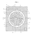
- Figure 1 is a plan view of an LED light emitting apparatus 10
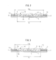
- Figure 2 is a cross-sectional view taken along ling A-A' in Figure 1
- Figure 3 is a cross-sectional view taken along ling B-B' in Figure 1 .
- a metal plate 5 is used as a mounting substrate, a circuit substrate 2 having a circular opening 2a in the center is placed on the metal plate 5, and a circular portion 5a of the metal plate 5, which is exposed through the opening 2a of the circuit substrate 2, is used as a circular device mounting region 7.
- An aluminum plate having good reflectivity is used as the metal substrate 5, and a transparent insulating layer or an insulating layer treated for high reflectivity is formed on the surface of the metal plate 5 to protect the metal plate 5, to improve the reflectivity of the metal plate 5, and to provide electrical insulation from the metal plate 5.
- the circular portion 5a of the metal plate 5 which forms the device mounting region 7 is an aluminum plate or a reflective layer 11 treated for high reflectivity.
- LED devices 1 are fixedly mounted on the reflective layer 11 in the device mounting region 7.
- LED connecting electrodes 6a and 6b (indicated by dashed lines in Figure 1 ), each with a gold-plated layer formed thereon, are provided as a pair of opposing electrodes on the circuit substrate 2 in such a manner as to surround the opening 2a.
- a sealing frame 3 formed from a reflective resin is provided around the periphery of the device mounting region 7 in such a manner as to cover the LED connecting electrodes 6a and 6b.
- a resist 13 is applied to cover the circuit substrate 2 outside the sealing frame 3. That is, the resist 13 has an opening 13a whose diameter is larger than the diameter of the opening 2a in the circuit substrate 2, and is formed so as to cover the entire surface of the circuit substrate 2 up to the edges thereof except where power connecting electrodes 6c and 6d are formed.
- the sealing frame 3 is formed so that its inner circumference covers the portion extending from the upper face of the circuit substrate 2 to the side face of the opening 2a and overlapping the outer circumference of the reflective layer 11 formed on the metal plate, and so that its outer circumference is located inside the opening 13a and covers the LED connecting electrodes 6a and 6b.
- the region surrounded by the sealing frame 3 is sealed with a sealing resin 9 such as a transparent resin or a phosphor resin.
- the power connecting electrodes 6c and 6d connected to the LED connecting electrodes 6a and 6b, respectively, are formed at positions outside the sealing frame 3 so as to oppose each other across the device mounting region 7.
- the LED devices 1 are top-electrode type LED devices. Connections between the electrodes of the LED devices 1 and connections from the LED devices 1 to the LED connecting electrodes 6a and 6b are made by wires 8.
- the plurality of LED devices 1 mounted in the device mounting region 7 are arranged to form a plurality of LED strings between the pair of LED connecting electrodes 6a and 6b provided at the top and bottom.
- LED strings each consisting of six LED devices 1 are formed in the center of the device mounting region 7, and an LED string of five LED devices, an LED string of four LED devices, and an LED string of three LED devices are formed one adjacent to another on each side of the center.
- the LED devices 1 are arranged in a near circular geometry in the device mounting region 7.
- the two LED strings each consisting of six LED devices 1 arranged in the center are connected in series by wires 8 to form a first LED device group L1 of twelve LED devices 1 between the pair of LED connecting electrodes 6a and 6b.
- the LED string of five LED devices, the LED string of four LED devices, and the LED string of three LED devices, arranged on each side of the center are also connected in series by wires 8 to form a second LED device group L2 on one side and a third LED device group L3 on the other side, each formed from twelve LED devices 1, between the pair of LED connecting electrodes 6a and 6b.
- the first LED device group L1, the second LED device group L2, and the third LED device group L3, each formed from twelve LED devices 1, are connected in parallel between the pair of LED connecting electrodes 6a and 6b.
- the three LED strings i.e., the LED string of five LED devices, the LED string of four LED devices, and the LED string of three LED devices, are connected in series.
- the metal plate 5 prepared by forming a high-reflectivity layer on a metal plate such as an aluminum plate is used as the mounting substrate, and the LED devices 1 are fixedly mounted directly on the reflective layer 11 formed on the metal plate 5; this serves to increase heat dissipation from the LED devices 1 and to produce light of high output power.
- the reflective layer 11 is formed in the device mounting region 7, and the reflective sealing frame 3 is provided around the device mounting region 7 in such a manner that the inner circumference of the sealing frame 3 overlaps the outer circumference of the reflective layer 11.
- the LED light emitting apparatus 10 since the device mounting region 7 is enclosed by only the reflective members, i.e., the reflective layer 11 and the reflective resin frame 3, the light emitted from the LED devices 1 is not absorbed by the opening 2a in the circuit substrate 2 nor is it absorbed by the gold-plated layers formed on the LED connecting electrodes 6a and 6b. As a result, in the LED light emitting apparatus 10, all the light emitted from the LED devices 1 is reflected by the reflective layer 11 and the reflective resin frame 3 (the reflective efficiency is extremely high), thus achieving a high radiative efficiency.
- the wire bondability of the LED devices 1 improves, which serves to increase the connection reliability. Accordingly, in the LED light emitting apparatus 10, the radiative efficiency can be increased while at the same time increasing the connection reliability.
- an enhanced reflective film such as a dielectric multilayer film
- the metal plate 5 is formed from a highly reflective material such as aluminum or silver
- such an enhanced reflective film need not necessarily be used, but use may be made of a transparent insulating film to provide insulation.
- the insulating layer is formed on the surface of the metal plate 5, and the LED devices 1 are fixedly mounted thereon.
- the top-electrode type LED devices can be fixedly mounted directly on the surface of the metal plate, but when the large number of LED devices 1 are mounted in the circular device mounting region 7 as shown in Figure 1 , the voltage applied between the terminals of the LED devices 1 may increase. Therefore, in the LED light emitting apparatus 10, the insulating layer is provided to ensure insulation for the LED devices 1.
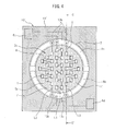
- Figure 4 is a plan view of an LED light emitting apparatus 10' as a modified example of the LED light emitting apparatus 10, and Figure 5 is a cross-sectional view taken along ling C-C' in Figure 4 .
- the difference between the LED light emitting apparatus 10' of Figure 4 and the LED light emitting apparatus 10 of Figure 1 lies in the pattern of the resist 13' formed in the LED light emitting apparatus 10' of Figure 4 ; otherwise, the configuration is the same as that of the LED light emitting apparatus 10 shown in Figure 1 .
- the resist 13' has an opening 13a, whose diameter is substantially the same as that of the opening 2a in the circuit substrate 2, and six openings 13b formed in positions where the LED devices 1 are connected to the LED connecting electrodes 6a and 6b by wires 8. That is, the resist 13' is formed so as to cover the LED connecting electrodes 6a and 6b everywhere except where the openings 13b are formed. Further, the resist 13' is formed so as to cover the entire surface of the circuit substrate 2 up to the edges thereof except where the power connecting electrodes 6c and 6d are formed. With this arrangement, the sealing frame 3 is formed so that its inner circumference is located inside the opening 13a of the resist 13' and so that its outer circumference covers the LED connecting electrodes 6a and 6b and overlaps a portion of the resist 13'.
- Figure 6 is a plan view of an alternative LED light emitting apparatus 20, and Figure 7 is a cross-sectional view taken along ling D-D' in Figure 6 .
- the alternative LED light emitting apparatus 20 shown in Figures 6 and 7 the same component elements as those in the LED light emitting apparatus 10 shown in Figures 1 and 2 are designated by the same reference numerals, and the description of such component elements will not be repeated here.
- the metal plate 5 is used as the mounting substrate, the circuit substrate 2 having a circular opening 2a in the center is placed on the metal plate 5, and the circular portion 5a of the metal plate 5 exposed through the opening 2a of the circuit substrate 2 is used as the circular device mounting region 7.
- a circuit substrate 2 having no openings is used as the mounting substrate, a circular reflective insulating layer 4 is formed in the center of the upper surface of the circuit substrate 2, and this circular reflective insulating layer 4 is used as the device mounting region 7.
- the reflective sealing frame 3 is formed so as to cover the LED connecting electrodes 6a and 6b on the upper surface of the circuit substrate 2 and so as to overlap the outer circumference of the reflective insulating layer 4. Further, in the LED light emitting apparatus 20, since the device mounting region 7 is enclosed by only the reflective members, i.e., the reflective insulating layer 4 and the reflective sealing frame 3, the light emitted from the LED devices 1 is not absorbed by the exposed portions of the circuit substrate 2 nor is it absorbed by the gold-plated layers formed on the LED connecting electrodes 6a and 6b. Furthermore, since the light emitted from the LED devices 1 is reflected by the reflective insulating layer 4 and the reflective sealing frame 3, the LED light emitting apparatus 20 achieves an extremely high reflective efficiency. In the LED light emitting apparatus 20, the reflective insulating layer 4 is formed from a white reflective resin layer formed by mixing reflective particles such as titanium oxide into a transparent resin, or from a white reflective insulating layer such as a ceramic ink layer.
- the arrangement of the LED devices 1, the connections made by the wires 8, the drive voltage supply, and the light-emitting driving operation are the same as those in the LED light emitting apparatus 10, the only difference being that the circuit substrate 2 is used as the mounting substrate and the reflective insulating layer 4 formed thereon is used as the device mounting region 7.
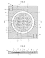
- Figure 8 is a plan view of a further alternative LED light emitting apparatus 30, and Figure 9 is a cross-sectional view taken along ling E-E' in Figure 8 .
- the same component elements as those in the LED light emitting apparatus 20 shown in Figures 6 and 7 are designated by the same reference numerals, and the description of such component elements will not be repeated here.
- the reflective insulating layer 4 is formed on the resin substrate of the circuit substrate 2, and this reflective insulating layer 4 is used as the device mounting region 7.
- a circular mounting electrode 6e is formed as a copper foil pattern in the center of the circuit substrate 2 independently of both the LED connecting electrodes 6a and 6b and the power connecting electrodes 6c and 6d.
- a silver-plated layer as a plated reflective layer 12 is formed on the mounting electrode 6e, and the plated reflective layer 12 is covered with a transparent insulating layer to form the device mounting region 7.
- the LED connecting electrodes 6a and 6b and the power connecting electrodes 6c and 6d formed by depositing copper foil patterns on the circuit substrate 2, are plated with gold to ensure good connections.
- the device mounting electrode 6e is formed so as to be electrically separated from both the LED connecting electrodes 6a and 6b and the power connecting electrodes 6c and 6d.
- the reflective sealing frame 3 is formed so as to cover the LED connecting electrodes 6a and 6b on the upper surface of the circuit substrate 2 and so as to overlap the outer circumference of the plated reflective layer 12. Further, in the LED light emitting apparatus 30, since the device mounting region 7 is enclosed by only the reflective members, i.e., the plated reflective layer 12 and the reflective sealing frame 3, the light emitted from the LED devices 1 is not absorbed by the exposed portions of the circuit substrate 2 nor is it absorbed by the gold-plated layers formed on the LED connecting electrodes 6a and 6b.
- the LED light emitting apparatus 30 since all the light emitted from the LED devices 1 is reflected by the plated reflective layer 12 and the reflective resin frame 3, the LED light emitting apparatus 30 achieves an extremely high reflective efficiency. Moreover, in the LED light emitting apparatus 30, since the mounting electrode 6e formed by depositing a copper foil pattern is used as the device mounting region 7, the structure serves to increase heat dissipation from the LED devices 1 fixedly mounted on the copper foil pattern.
- any of the above-described LED light emitting apparatus 10, 20, and 30 can be applied as an LED light emitting apparatus that produces white light by wavelength conversion using a phosphor layer.
- an LED light emitting apparatus that produces white light can be constructed by using blue LEDs as the LED devices 1 and using in combination a YAG phosphor layer as the sealing resin 9.
- An LED light emitting apparatus that produces white light can also be constructed by using ultraviolet LEDs as the LED devices 1 and using in combination an RGB phosphor layer as the sealing resin 9.
- the reflective layer is formed in the device mounting region, the opposing electrodes are plated with gold, and the reflective sealing frame is formed around the device mounting region in such a manner that the inner circumference of the sealing frame overlaps the outer circumference of the reflective layer.
Landscapes
- Led Device Packages (AREA)
Abstract
Description
- The present invention relates to an LED light emitting apparatus constructed by mounting a plurality of LED devices in a device mounting region enclosed by a sealing frame, and more particularly to an LED light emitting apparatus constructed so as to be able to achieve a high radiative efficiency by forming a reflective layer in the device mounting region and mounting the plurality of LED devices on the reflective layer.
- In recent years, LED devices as semiconductor devices have come into wide use in applications such as color display backlighting, illumination, and the like, because of their long life, excellent driving characteristics, compact size, and good luminous efficacy as well as their capability to produce crisp, bright colors.
- Among others, there have been proposed a variety of LED light emitting apparatus for producing light of high brightness by mounting a plurality of LED devices in a device mounting region of a predefined shape (for example, refer to
patent documents 1 and 2). -
Figure 10 is a plan view showing a light-emitting portion of an LED light emitting apparatus disclosed inpatent document 1. InFigure 10 , the diagram is simplified in part and, for ease of comparison, some of the component elements are referred to by the same names as those used in the present patent application. - As shown in
Figure 10 , the LEDlight emitting apparatus 100 includes a circular device mounting region which is divided into four smaller regions, i.e., the first mounting region 102a, the second mounting region 102b, the third mounting region 102c, and the fourth mounting region 102d. The circular device mounting region is surrounded by two power electrodes 103a and 103b and three relay electrodes 104a, 104b, and 104c. - The two mounting regions 102b and 102c near the center each accommodate twenty LED devices 101 in two strings of ten LED devices 101 arranged in a staggered fashion. The ten LED devices 101 in each string are connected in series by
wires 108. Further, the two strings of series-connected LED devices are connected to the relay electrodes 104a, 104b and 104c bywires 108. More specifically, in the mounting region 102b, the two LED strings each consisting of ten LED devices connected in series are connected in parallel between the relay electrodes 104a and 104c, while in the mounting region 102c, the two LED strings each consisting of ten LED devices connected in series are connected in parallel between the relay electrodes 104b and 104c. - Similarly, the two mounting regions 102a and 102d on both sides each accommodate twelve LED devices 101 in two strings of six LED devices 101 arranged in a staggered fashion. The six LED devices 101 in each string are connected in series by
wires 108. Further, the two strings of series-connected LED devices are connected between the relay electrode 104a and the power electrode 103a or between the relay electrode 104b and the power electrode 103b bywires 108. More specifically, in the mounting region 102a, the two LED strings each consisting of six LED devices connected in series are connected in parallel between the relay electrode 104a and the power electrode 103a, while in the mounting region 102d, the two LED strings each consisting of six LED devices connected in series are connected in parallel between the relay electrode 104b and the power electrode 103b. - In the above configuration, when the power electrode 103a is designated as the positive electrode (+) and the power electrode 103b as the negative electrode (-), two LED strings each consisting of six LED devices connected in series are mounted in each of the mounting regions 102a and 102d and connected between the power electrodes 103a and 103b, while on the other hand, two LED strings each consisting of ten LED devices connected in series are mounted in each of the mounting regions 102b and 102c and connected between the power electrodes 103a and 103b. The LED strings mounted in the respective mounting regions are all connected in series between the power electrodes 103a and 103b via the relay electrodes 104a, 104c, and 104b. Therefore, the total number of the series-connected LED devices 101 in the four mounting regions is given as 6 + 10 + 10 + 6 = 32; if the drive voltage of each LED device is 3 V, then 3 x 32 = 96 V. This means that when the voltage of 96 V is applied between the power electrodes 103a and 103b, all the LED devices 101 emit light.
-
Figure 11 is a perspective view showing an LED light emitting apparatus disclosed inpatent document 2. InFigure 11 , the diagram is simplified in part and, for ease of comparison, some of the component elements are referred to by the same names as those used in the present patent application. - As shown in
Figure 11 , the LEDlight emitting apparatus 200 includes arectangular circuit substrate 201 havingconductive interconnection patterns 203A, 203B, and 203C on its upper surface, and a plurality ofLED devices 204 mounted on theconductive interconnection pattern 203A. A sealingframe 202 formed from a reflective white resin for reflecting light emitted from theLED devices 204 is provided so as to surround theLED devices 204. TheLED devices 204 are electrically connected to theconductive interconnection patterns 203A and 203B bywires 205. The conductive interconnection pattern 203C is provided as a guide mark to indicate the polarity. - The
conductive interconnection pattern 203A is formed so that the region in which theLED devices 204 are mounted and the region to which thewires 205 are connected are connected together in portions buried under the sealing frame 202 (though not shown here). Thesealing frame 202 is provided so that portions of the region of theconductive interconnection pattern 203A on which theLED devices 204 are mounted, regions 201A exposed on thecircuit substrate 201 between theconductive interconnection patterns 203A and 203B to which thewires 205 are connected, and portions of thewires 205 connecting theLED devices 204 to theconductive interconnection patterns 203A and 203B are buried under the sealingframe 202. - Since portions of the
wires 205 and the regions 201A exposed on thecircuit substrate 201 are buried under the sealingframe 202, the amount of light emitted from theLED devices 204 and absorbed by thewires 205 and the regions 201A exposed on thecircuit substrate 201 is reduced, thereby increasing light extraction efficiency. -
- Patent document 1: Japanese Unexamined Patent Publication No.
2010-287656 - Patent document 2: Japanese Unexamined Patent Publication No.
2009-164157 - In an LED light emitting apparatus constructed by mounting a plurality of LED devices on a substrate having a device mounting region and a pair of opposing electrodes disposed outside the device mounting region and by providing a sealing frame around the device mounting region while connecting the LED devices to the opposing electrodes by wires, there is a need to increase the light extraction efficiency from the device mounting region while at the same time enhancing the reliability of connections to the LED devices.
- In the LED
light emitting apparatus 100 disclosed inpatent document 1, the plurality of LED devices are arranged for mounting in a near circular geometry in the device mounting region having a circular shape, but since the device mounting region is split into a plurality of portions, portions of poor reflectivity are left between the split portions of the device mounting region. As a result, the reflectivity of the device mounting region as a whole decreases, resulting in the problem that the light extraction efficiency does not increase. Furthermore, because of the absence of a reflective frame for gathering light scattering from the device mounting region and for directing it in the forward direction, there is also the problem that it is not possible to increase the light extraction efficiency as a whole. - In the LED
light emitting apparatus 200 disclosed inpatent document 2, since the region in which theLED devices 204 are mounted and the region to which thewires 205 are connected are formed integrally as theconductive interconnection pattern 203A, the surfaces of these regions are treated under the same conditions. However, the conditions required for the surface treatment of the LED device mounting region (the treatment for increasing the light extraction efficiency) are different from the conditions required for the surface treatment of the wire connecting region (the treatment for reliably connecting the wires). As a result, in the LEDlight emitting apparatus 200, it is difficult to increase the light extraction efficiency while at the same time enhancing the reliability of connections to the LED devices. - Generally, in the case of a metallic film, a white or whitish film such as a silver or aluminum film is preferred for use as a reflector. On the other hand, a representative metal that has high connection reliability is gold. For example, when forming the
conductive interconnection pattern 203A by plating, the region to which thewires 205 are to be connected is plated with gold so that high connection reliability can be obtained. However, in this case, the gold plating is also applied at the same time to the region of theconductive interconnection pattern 203A where theLED devices 204 are to be mounted. Since the layer of gold plating has poor reflectivity and absorbs light emitted from theLED devices 204, high radiative efficiency cannot be obtained. - When silver plating is applied to the
conductive interconnection pattern 203A so that the region in which theLED devices 204 are mounted will have high reflectivity, the reflectivity of the region in which theLED devices 204 are mounted improves. However, in this case, the silver plating is also applied at the same time to the region of theconductive interconnection pattern 203A where theLED devices 204 are to be mounted. Since the layer of silver plating has poor bonding to thewires 205, the reliability of connections to the LED devices degrades. - As can be seen from the above, there is a need to form a gold layer having good bonding in the region of the
conductive interconnection pattern 203A to which the wire leads are to be connected, and to form a silver layer having good reflectivity in the region in which the LED devices are to be mounted. However, in the LEDlight emitting apparatus 200, the region in which theLED devices 204 are mounted and the region to which thewires 205 are connected are formed integrally as theconductive interconnection pattern 203A. As a result, in the LEDlight emitting apparatus 200, it is difficult to increase the light extraction efficiency while at the same time enhancing the reliability of connections to the LED devices. (Figure 9A inpatent document 2 shows a structure in which a silver-plated layer is formed on an integrally formed wiring electrode pattern.) - An object of the present invention is to provide an LED light emitting apparatus that makes it possible to increase light extraction efficiency while at the same time enhancing the reliability of connections to LED devices.
- The LED light emitting apparatus includes a mounting substrate having a device mounting region in which a reflective layer is formed, a plurality of LED devices mounted in the device mounting region, a pair of opposing electrodes with a gold-plated layer formed thereon, the pair of opposing electrodes being arranged around the device mounting region and being connected to the plurality of LED devices by means of wire bonding, and a sealing frame formed around the device mounting region so as to cover the pair of opposing electrodes, wherein an inner circumference of the sealing frame overlaps an outer circumference of the reflective layer.
- According to the above configuration, the opposing electrodes are plated with gold to improve the wire bondability of the LED devices thereby enhancing the reliability of connections, while on the other hand, the reflective layer is formed in the device mounting region and the sealing frame is formed around the device mounting region in such a manner that the inner circumference of the sealing frame overlaps the outer circumference of the reflective layer and thus covers the side face of the opening formed in the circuit substrate, minimizing the loss of light therein; with this structure, the light extraction efficiency from the device mounting region can be greatly increased.
- Preferably, in the LED light emitting apparatus, the reflective layer is a metal plate that covers a bottom face exposed through an opening formed in a circuit substrate on which the pair of opposing electrodes is formed, and the sealing frame is formed so as to cover a portion extending from an upper face of the circuit substrate to a side face of the opening and further to a surface of the metal plate.
- Preferably, in the LED light emitting apparatus, the metal plate is an aluminum plate.
- Preferably, in the LED light emitting apparatus, the reflective layer is an insulating film treated for high reflectivity formed on the surface of the metal plate.
- According to the above configuration, since the mounting substrate that provides the device mounting region is constructed from a metal plate having excellent heat dissipation characteristics, and since the opposing electrodes are formed as wiring electrodes on the circuit substrate, the gold plating of the opposing electrodes and the formation of a high-reflectivity insulating layer in the device mounting region can be performed independently of each other; as a result, not only the light extraction efficiency from the device mounting region and the reliability of connections to the LED devices but also the heat dissipation performance can be enhanced.
- Preferably, in the LED light emitting apparatus, the reflective layer is a white reflective insulating layer formed on the circuit substrate on which the pair of opposing electrodes is formed, and the sealing frame is formed so as to cover a portion extending from the upper face of the circuit substrate and overlapping the outer circumference of the white reflective layer.
- Preferably, in the LED light emitting apparatus, the white reflective layer is a ceramic ink layer or a white reflective resin layer.
- Preferably, in the LED light emitting apparatus, the white reflective layer is formed by depositing a silver-plated layer and a transparent insulating layer one on top of the other on the circuit substrate on which the pair of opposing electrodes is formed.
- Preferably, in the LED light emitting apparatus, the reflective layer formed in the device mounting region has a circular shape.
- Preferably, in the LED light emitting apparatus, the sealing frame is formed from a reflective white resin.
- Preferably, the LED light emitting apparatus further comprises a phosphor layer, formed inside the sealing frame, for modulating light emitted from the plurality of LED devices and thereby converting the light into white light.
- Preferably, in the LED light emitting apparatus, the plurality of LED devices are blue LED devices, and the phosphor layer is a YAG phosphor layer.
- Preferably, in the LED light emitting apparatus, the plurality of LED devices are ultraviolet LED devices, and the phosphor layer is an RGB phosphor layer.
- Preferably, the LED light emitting apparatus further includes a resist layer intervening between the pair of opposing electrodes and the sealing frame and having openings at positions where the plurality of LED devices are connected to the opposing electrodes by means of wire bonding.
- According to the LED light emitting apparatus described above, the light extraction efficiency can be increased while at the same time enhancing the reliability of connections to the LED devices.
-
-
Figure 1 is a plan view of an LEDlight emitting apparatus 10. -
Figure 2 is a cross-sectional view taken along ling A-A' inFigure 1 . -
Figure 3 is a cross-sectional view taken along ling B-B' inFigure 1 . -
Figure 4 is a plan view of an LED light emitting apparatus 10' as a modified example of the LEDlight emitting apparatus 10. -
Figure 5 is a cross-sectional view taken along ling C-C' inFigure 4 . -
Figure 6 is a plan view of an alternative LEDlight emitting apparatus 20. -
Figure 7 is a cross-sectional view taken along ling D-D' inFigure 6 . -
Figure 8 is a plan view of a further alternative LEDlight emitting apparatus 30. -
Figure 9 is a cross-sectional view taken along ling E-E' inFigure 8 . -
Figure 10 is a plan view showing a light-emitting portion of an LED light emitting apparatus disclosed inpatent document 1. -
Figure 11 is a perspective view showing an LED light emitting apparatus disclosed inpatent document 2. - LED light emitting apparatus will be described below with reference to the drawings. It will, however, be noted that the technical scope of the present invention is not limited by any particular embodiment described herein but extends to the inventions described in the appended claims and their equivalents. Further, in the description of the drawings, the same or corresponding component elements are designated by the same reference numerals, and the description of such component elements, once given, will not be repeated thereafter.
-
Figure 1 is a plan view of an LEDlight emitting apparatus 10,Figure 2 is a cross-sectional view taken along ling A-A' inFigure 1 , andFigure 3 is a cross-sectional view taken along ling B-B' inFigure 1 . - As shown in
Figures 1 and2 , in the LEDlight emitting apparatus 10, ametal plate 5 is used as a mounting substrate, acircuit substrate 2 having acircular opening 2a in the center is placed on themetal plate 5, and acircular portion 5a of themetal plate 5, which is exposed through theopening 2a of thecircuit substrate 2, is used as a circulardevice mounting region 7. An aluminum plate having good reflectivity is used as themetal substrate 5, and a transparent insulating layer or an insulating layer treated for high reflectivity is formed on the surface of themetal plate 5 to protect themetal plate 5, to improve the reflectivity of themetal plate 5, and to provide electrical insulation from themetal plate 5. - The
circular portion 5a of themetal plate 5 which forms thedevice mounting region 7 is an aluminum plate or areflective layer 11 treated for high reflectivity.LED devices 1 are fixedly mounted on thereflective layer 11 in thedevice mounting region 7.LED connecting electrodes Figure 1 ), each with a gold-plated layer formed thereon, are provided as a pair of opposing electrodes on thecircuit substrate 2 in such a manner as to surround theopening 2a. A sealingframe 3 formed from a reflective resin is provided around the periphery of thedevice mounting region 7 in such a manner as to cover theLED connecting electrodes - A resist 13 is applied to cover the
circuit substrate 2 outside the sealingframe 3. That is, the resist 13 has anopening 13a whose diameter is larger than the diameter of theopening 2a in thecircuit substrate 2, and is formed so as to cover the entire surface of thecircuit substrate 2 up to the edges thereof except wherepower connecting electrodes - The sealing
frame 3 is formed so that its inner circumference covers the portion extending from the upper face of thecircuit substrate 2 to the side face of theopening 2a and overlapping the outer circumference of thereflective layer 11 formed on the metal plate, and so that its outer circumference is located inside theopening 13a and covers theLED connecting electrodes frame 3 is sealed with a sealingresin 9 such as a transparent resin or a phosphor resin. Thepower connecting electrodes LED connecting electrodes frame 3 so as to oppose each other across thedevice mounting region 7. TheLED devices 1 are top-electrode type LED devices. Connections between the electrodes of theLED devices 1 and connections from theLED devices 1 to theLED connecting electrodes wires 8. - The plurality of
LED devices 1 mounted in thedevice mounting region 7 are arranged to form a plurality of LED strings between the pair ofLED connecting electrodes LED devices 1 are formed in the center of thedevice mounting region 7, and an LED string of five LED devices, an LED string of four LED devices, and an LED string of three LED devices are formed one adjacent to another on each side of the center. As a whole, theLED devices 1 are arranged in a near circular geometry in thedevice mounting region 7. - The two LED strings each consisting of six
LED devices 1 arranged in the center are connected in series bywires 8 to form a first LED device group L1 of twelveLED devices 1 between the pair ofLED connecting electrodes wires 8 to form a second LED device group L2 on one side and a third LED device group L3 on the other side, each formed from twelveLED devices 1, between the pair ofLED connecting electrodes - As described above, the first LED device group L1, the second LED device group L2, and the third LED device group L3, each formed from twelve
LED devices 1, are connected in parallel between the pair ofLED connecting electrodes Figure 1 , when connecting many LED strings in series, it is easier to interconnect the electrodes of theLED devices 1 bywires 8 if the electrodes of theLED devices 1 are oriented in parallel to the direction across which theLED connecting electrodes - In the LED
light emitting apparatus 10, themetal plate 5 prepared by forming a high-reflectivity layer on a metal plate such as an aluminum plate is used as the mounting substrate, and theLED devices 1 are fixedly mounted directly on thereflective layer 11 formed on themetal plate 5; this serves to increase heat dissipation from theLED devices 1 and to produce light of high output power. Further, in the LEDlight emitting apparatus 10, thereflective layer 11 is formed in thedevice mounting region 7, and thereflective sealing frame 3 is provided around thedevice mounting region 7 in such a manner that the inner circumference of the sealingframe 3 overlaps the outer circumference of thereflective layer 11. Furthermore, in the LEDlight emitting apparatus 10, since thedevice mounting region 7 is enclosed by only the reflective members, i.e., thereflective layer 11 and thereflective resin frame 3, the light emitted from theLED devices 1 is not absorbed by theopening 2a in thecircuit substrate 2 nor is it absorbed by the gold-plated layers formed on theLED connecting electrodes light emitting apparatus 10, all the light emitted from theLED devices 1 is reflected by thereflective layer 11 and the reflective resin frame 3 (the reflective efficiency is extremely high), thus achieving a high radiative efficiency. - In the LED
light emitting apparatus 10, since the gold-plated layer is formed on each of theLED connecting electrodes LED devices 1 improves, which serves to increase the connection reliability. Accordingly, in the LEDlight emitting apparatus 10, the radiative efficiency can be increased while at the same time increasing the connection reliability. - For the high-reflective layer formed as the
reflective layer 11 in thedevice mounting region 7, use is preferably made of an enhanced reflective film such as a dielectric multilayer film; however, when themetal plate 5 is formed from a highly reflective material such as aluminum or silver, such an enhanced reflective film need not necessarily be used, but use may be made of a transparent insulating film to provide insulation. - In the LED
light emitting apparatus 10, the insulating layer is formed on the surface of themetal plate 5, and theLED devices 1 are fixedly mounted thereon. Generally, the top-electrode type LED devices can be fixedly mounted directly on the surface of the metal plate, but when the large number ofLED devices 1 are mounted in the circulardevice mounting region 7 as shown inFigure 1 , the voltage applied between the terminals of theLED devices 1 may increase. Therefore, in the LEDlight emitting apparatus 10, the insulating layer is provided to ensure insulation for theLED devices 1. -
Figure 4 is a plan view of an LED light emitting apparatus 10' as a modified example of the LEDlight emitting apparatus 10, andFigure 5 is a cross-sectional view taken along ling C-C' inFigure 4 . - The difference between the LED light emitting apparatus 10' of
Figure 4 and the LEDlight emitting apparatus 10 ofFigure 1 lies in the pattern of the resist 13' formed in the LED light emitting apparatus 10' ofFigure 4 ; otherwise, the configuration is the same as that of the LEDlight emitting apparatus 10 shown inFigure 1 . - In the LED light emitting apparatus 10' shown in
Figure 4 , the resist 13' has anopening 13a, whose diameter is substantially the same as that of theopening 2a in thecircuit substrate 2, and sixopenings 13b formed in positions where theLED devices 1 are connected to theLED connecting electrodes wires 8. That is, the resist 13' is formed so as to cover theLED connecting electrodes openings 13b are formed. Further, the resist 13' is formed so as to cover the entire surface of thecircuit substrate 2 up to the edges thereof except where thepower connecting electrodes frame 3 is formed so that its inner circumference is located inside theopening 13a of the resist 13' and so that its outer circumference covers theLED connecting electrodes - In the LED light emitting apparatus 10' shown in
Figure 4 , since the area where the sealingframe 3 contacts the resist 13' is larger than that in the LEDlight emitting apparatus 10 ofFigure 1 , the two members can be bonded together more firmly, and the reliability of the LED light emitting apparatus increases. -
Figure 6 is a plan view of an alternative LEDlight emitting apparatus 20, andFigure 7 is a cross-sectional view taken along ling D-D' inFigure 6 . In the alternative LEDlight emitting apparatus 20 shown inFigures 6 and 7 , the same component elements as those in the LEDlight emitting apparatus 10 shown inFigures 1 and2 are designated by the same reference numerals, and the description of such component elements will not be repeated here. - In the LED
light emitting apparatus 10, themetal plate 5 is used as the mounting substrate, thecircuit substrate 2 having acircular opening 2a in the center is placed on themetal plate 5, and thecircular portion 5a of themetal plate 5 exposed through theopening 2a of thecircuit substrate 2 is used as the circulardevice mounting region 7. By contrast, in the LEDlight emitting apparatus 20, acircuit substrate 2 having no openings is used as the mounting substrate, a circular reflective insulatinglayer 4 is formed in the center of the upper surface of thecircuit substrate 2, and this circular reflective insulatinglayer 4 is used as thedevice mounting region 7. - In the LED
light emitting apparatus 20, thereflective sealing frame 3 is formed so as to cover theLED connecting electrodes circuit substrate 2 and so as to overlap the outer circumference of the reflective insulatinglayer 4. Further, in the LEDlight emitting apparatus 20, since thedevice mounting region 7 is enclosed by only the reflective members, i.e., the reflective insulatinglayer 4 and thereflective sealing frame 3, the light emitted from theLED devices 1 is not absorbed by the exposed portions of thecircuit substrate 2 nor is it absorbed by the gold-plated layers formed on theLED connecting electrodes LED devices 1 is reflected by the reflective insulatinglayer 4 and thereflective sealing frame 3, the LEDlight emitting apparatus 20 achieves an extremely high reflective efficiency. In the LEDlight emitting apparatus 20, the reflective insulatinglayer 4 is formed from a white reflective resin layer formed by mixing reflective particles such as titanium oxide into a transparent resin, or from a white reflective insulating layer such as a ceramic ink layer. - In the LED
light emitting apparatus 20, the arrangement of theLED devices 1, the connections made by thewires 8, the drive voltage supply, and the light-emitting driving operation are the same as those in the LEDlight emitting apparatus 10, the only difference being that thecircuit substrate 2 is used as the mounting substrate and the reflective insulatinglayer 4 formed thereon is used as thedevice mounting region 7. -
Figure 8 is a plan view of a further alternative LEDlight emitting apparatus 30, andFigure 9 is a cross-sectional view taken along ling E-E' inFigure 8 . In the further alternative LEDlight emitting apparatus 30 shown inFigures 8 and 9 , the same component elements as those in the LEDlight emitting apparatus 20 shown inFigures 6 and 7 are designated by the same reference numerals, and the description of such component elements will not be repeated here. - In the LED
light emitting apparatus 20, the reflective insulatinglayer 4 is formed on the resin substrate of thecircuit substrate 2, and this reflective insulatinglayer 4 is used as thedevice mounting region 7. By contrast, in the LEDlight emitting apparatus 30, acircular mounting electrode 6e is formed as a copper foil pattern in the center of thecircuit substrate 2 independently of both theLED connecting electrodes power connecting electrodes reflective layer 12 is formed on the mountingelectrode 6e, and the platedreflective layer 12 is covered with a transparent insulating layer to form thedevice mounting region 7. Furthermore, theLED connecting electrodes power connecting electrodes circuit substrate 2, are plated with gold to ensure good connections. Such an arrangement is made possible because thedevice mounting electrode 6e is formed so as to be electrically separated from both theLED connecting electrodes power connecting electrodes - In the LED
light emitting apparatus 30, thereflective sealing frame 3 is formed so as to cover theLED connecting electrodes circuit substrate 2 and so as to overlap the outer circumference of the platedreflective layer 12.
Further, in the LEDlight emitting apparatus 30, since thedevice mounting region 7 is enclosed by only the reflective members, i.e., the platedreflective layer 12 and thereflective sealing frame 3, the light emitted from theLED devices 1 is not absorbed by the exposed portions of thecircuit substrate 2 nor is it absorbed by the gold-plated layers formed on theLED connecting electrodes light emitting apparatus 30, since all the light emitted from theLED devices 1 is reflected by the platedreflective layer 12 and thereflective resin frame 3, the LEDlight emitting apparatus 30 achieves an extremely high reflective efficiency. Moreover, in the LEDlight emitting apparatus 30, since the mountingelectrode 6e formed by depositing a copper foil pattern is used as thedevice mounting region 7, the structure serves to increase heat dissipation from theLED devices 1 fixedly mounted on the copper foil pattern. - Any of the above-described LED
light emitting apparatus LED devices 1 and using in combination a YAG phosphor layer as the sealingresin 9. An LED light emitting apparatus that produces white light can also be constructed by using ultraviolet LEDs as theLED devices 1 and using in combination an RGB phosphor layer as the sealingresin 9. - In the above-described LED
light emitting apparatus light emitting apparatus light emitting apparatus light emitting apparatus -
- 1
- LED DEVICE
- 2
- CIRCUIT SUBSTRATE
- 2a
- OPENING
- 3
- SEALING FRAME
- 4
- INSULATING REFLECTIVE LAYER
- 5
- METAL PLATE
- 5a
- CIRCULAR PORTION
- 6a, 6b
- LED CONNECTING ELECTRODE
- 6c, 6d
- POWER CONNECTING ELECTRODE
- 6e
- MOUNTING ELECTRODE
- 7
- DEVICE MOUNTING REGION
- 8
- WIRE
- 9
- SEALING RESIN
- 10, 20, 30
- LED LIGHT EMITTING APPARATUS
- 11
- REFLECTIVE LAYER
- 12
- PLATED REFLECTIVE LAYER
- 13, 13'
- RESIST
- 13a, 13b
- OPENING
Claims (13)
- An LED light emitting apparatus comprising:a mounting substrate having a device mounting region in which a reflective layer is formed;a plurality of LED devices mounted in said device mounting region;a pair of opposing electrodes with a gold-plated layer formed thereon, said pair of opposing electrodes being arranged around said device mounting region and being connected to said plurality of LED devices by means of wire bonding; anda sealing frame formed around said device mounting region so as to cover said pair of opposing electrodes,wherein an inner circumference of said sealing frame overlaps an outer circumference of said reflective layer.
- The LED light emitting apparatus according to claim 1, wherein said reflective layer is a metal plate that covers a bottom face exposed through an opening formed in a circuit substrate on which said pair of opposing electrodes is formed, and wherein said sealing frame is formed so as to cover a portion extending from an upper face of said circuit substrate to a side face of said opening and further to a surface of said metal plate.
- The LED light emitting apparatus according to claim 2, wherein said metal plate is an aluminum plate.
- The LED light emitting apparatus according to claim 2 or 3, wherein said reflective layer is an insulating film treated for high reflectivity formed on the surface of said metal plate.
- The LED light emitting apparatus according to claim 1, wherein said reflective layer is a white reflective insulating layer formed on a circuit substrate on which said pair of opposing electrodes is formed, and wherein said sealing frame is formed so as to cover a portion extending from an upper face of said circuit substrate and overlapping the outer circumference of said white reflective layer.
- The LED light emitting apparatus according to claim 5, wherein said white reflective layer is a ceramic ink layer or a white reflective resin layer.
- The LED light emitting apparatus according to claim 5, wherein said white reflective layer is formed by depositing a silver-plated layer and a transparent insulating layer one on top of the other on said circuit substrate on which said pair of opposing electrodes is formed.
- The LED light emitting apparatus according to any one of claims 1 to 7, wherein said reflective layer formed in said device mounting region has a circular shape.
- The LED light emitting apparatus according to any one of claims 1 to 8, wherein said sealing frame is formed from a reflective white resin.
- The LED light emitting apparatus according to any one of claims 1 to 9, further comprising a phosphor layer, formed inside said sealing frame, for modulating light emitted from said plurality of LED devices and thereby converting said light into white light.
- The LED light emitting apparatus according to claim 10, wherein said plurality of LED devices are blue LED devices, and said phosphor layer is a YAG phosphor layer.
- The LED light emitting apparatus according to claim 10, wherein said plurality of LED devices are ultraviolet LED devices, and said phosphor layer is an RGB phosphor layer.
- The LED light emitting apparatus according to claim 1, further comprising a resist layer intervening between said pair of opposing electrodes and said sealing frame and having openings at positions where said plurality of LED devices are connected to said opposing electrodes by means of wire bonding.
Applications Claiming Priority (2)
| Application Number | Priority Date | Filing Date | Title |
|---|---|---|---|
| JP2012087358 | 2012-04-06 | ||
| PCT/JP2013/057551 WO2013150882A1 (en) | 2012-04-06 | 2013-03-15 | Led light emitting apparatus |
Publications (3)
| Publication Number | Publication Date |
|---|---|
| EP2835837A1 true EP2835837A1 (en) | 2015-02-11 |
| EP2835837A4 EP2835837A4 (en) | 2015-11-18 |
| EP2835837B1 EP2835837B1 (en) | 2019-08-07 |
Family
ID=49300376
Family Applications (1)
| Application Number | Title | Priority Date | Filing Date |
|---|---|---|---|
| EP13772536.2A Active EP2835837B1 (en) | 2012-04-06 | 2013-03-15 | Light emitting device with light emitting diodes |
Country Status (5)
| Country | Link |
|---|---|
| US (1) | US20150091029A1 (en) |
| EP (1) | EP2835837B1 (en) |
| JP (1) | JPWO2013150882A1 (en) |
| CN (1) | CN204375793U (en) |
| WO (1) | WO2013150882A1 (en) |
Families Citing this family (9)
| Publication number | Priority date | Publication date | Assignee | Title |
|---|---|---|---|---|
| JP6336787B2 (en) * | 2014-03-12 | 2018-06-06 | シチズン電子株式会社 | Light source unit |
| JP6366337B2 (en) * | 2014-04-23 | 2018-08-01 | シチズン電子株式会社 | LED light emitting device and manufacturing method thereof |
| JP6344058B2 (en) * | 2014-05-23 | 2018-06-20 | 東芝ライテック株式会社 | Light emitting module and lighting device |
| JP6381327B2 (en) | 2014-07-17 | 2018-08-29 | シチズン電子株式会社 | LED light emitting device and manufacturing method thereof |
| JP6256700B2 (en) * | 2014-11-11 | 2018-01-10 | 豊田合成株式会社 | Light emitting device |
| JP6486099B2 (en) * | 2014-12-19 | 2019-03-20 | シチズン電子株式会社 | LED light emitting module |
| US10403607B2 (en) * | 2015-03-16 | 2019-09-03 | Bridgelux Inc. | Chip-on-board design with color mixing |
| JP6982489B2 (en) * | 2017-12-22 | 2021-12-17 | シチズン電子株式会社 | Light emitting device and manufacturing method of light emitting device |
| KR102873277B1 (en) * | 2020-05-08 | 2025-10-20 | 삼성전자주식회사 | A light-generating device |
Family Cites Families (21)
| Publication number | Priority date | Publication date | Assignee | Title |
|---|---|---|---|---|
| JP2006005290A (en) * | 2004-06-21 | 2006-01-05 | Citizen Electronics Co Ltd | Light emitting diode |
| AU2005332456B2 (en) * | 2005-05-31 | 2010-02-25 | Mitsubishi Heavy Industries, Ltd. | Structure of slewing ring bearing |
| JP5066333B2 (en) * | 2005-11-02 | 2012-11-07 | シチズン電子株式会社 | LED light emitting device. |
| JP5270861B2 (en) * | 2007-05-15 | 2013-08-21 | シチズン電子株式会社 | Backlight light source |
| JP5119917B2 (en) | 2007-12-28 | 2013-01-16 | 日亜化学工業株式会社 | Light emitting device |
| US8049237B2 (en) * | 2007-12-28 | 2011-11-01 | Nichia Corporation | Light emitting device |
| JP5345363B2 (en) * | 2008-06-24 | 2013-11-20 | シャープ株式会社 | Light emitting device |
| US8506103B2 (en) * | 2008-11-26 | 2013-08-13 | Keiji Iimura | Semiconductor lamp and light bulb type LED lamp |
| JP2010199547A (en) * | 2009-01-30 | 2010-09-09 | Nichia Corp | Light emitting device and method of manufacturing same |
| JP2010287656A (en) | 2009-06-10 | 2010-12-24 | Toshiba Corp | Method for manufacturing solid-state imaging device |
| JP2011009298A (en) * | 2009-06-23 | 2011-01-13 | Citizen Electronics Co Ltd | Light-emitting diode light source device |
| TWI354365B (en) * | 2009-08-26 | 2011-12-11 | Quasioptical led package structure for increasing | |
| JP5623062B2 (en) * | 2009-11-13 | 2014-11-12 | シャープ株式会社 | Light emitting device and manufacturing method thereof |
| JP5729375B2 (en) * | 2010-02-25 | 2015-06-03 | 旭硝子株式会社 | Light emitting device |
| JP5459555B2 (en) * | 2010-03-05 | 2014-04-02 | 東芝ライテック株式会社 | Light emitting module and lighting device |
| US8820950B2 (en) * | 2010-03-12 | 2014-09-02 | Toshiba Lighting & Technology Corporation | Light emitting device and illumination apparatus |
| JP5768435B2 (en) * | 2010-04-16 | 2015-08-26 | 日亜化学工業株式会社 | Light emitting device |
| JP5842813B2 (en) * | 2010-04-16 | 2016-01-13 | 日亜化学工業株式会社 | Light emitting device and method for manufacturing light emitting device |
| JP2013140823A (en) * | 2010-04-16 | 2013-07-18 | Nichia Chem Ind Ltd | Light-emitting device |
| JP5612991B2 (en) * | 2010-09-30 | 2014-10-22 | シャープ株式会社 | LIGHT EMITTING DEVICE AND LIGHTING DEVICE HAVING THE SAME |
| US8575639B2 (en) * | 2011-02-16 | 2013-11-05 | Cree, Inc. | Light emitting devices for light emitting diodes (LEDs) |
-
2013
- 2013-03-15 JP JP2014509097A patent/JPWO2013150882A1/en active Pending
- 2013-03-15 US US14/390,642 patent/US20150091029A1/en not_active Abandoned
- 2013-03-15 CN CN201390000376.1U patent/CN204375793U/en not_active Expired - Lifetime
- 2013-03-15 EP EP13772536.2A patent/EP2835837B1/en active Active
- 2013-03-15 WO PCT/JP2013/057551 patent/WO2013150882A1/en not_active Ceased
Also Published As
| Publication number | Publication date |
|---|---|
| JPWO2013150882A1 (en) | 2015-12-17 |
| US20150091029A1 (en) | 2015-04-02 |
| EP2835837B1 (en) | 2019-08-07 |
| WO2013150882A1 (en) | 2013-10-10 |
| EP2835837A4 (en) | 2015-11-18 |
| CN204375793U (en) | 2015-06-03 |
Similar Documents
| Publication | Publication Date | Title |
|---|---|---|
| EP2835837B1 (en) | Light emitting device with light emitting diodes | |
| US10707188B2 (en) | Light emitting device | |
| CN103430339B (en) | Substrate, light-emitting device, and illumination device | |
| EP2341560B1 (en) | Light emitting device | |
| US9484514B2 (en) | Light-emitting device | |
| TW200931684A (en) | Light-emitting element and light-emitting device using the same | |
| US20140185294A1 (en) | Light emitting device | |
| TW201727945A (en) | Illuminating device | |
| WO2011129203A1 (en) | Light-emitting device | |
| CN109585631B (en) | light emitting device | |
| US9960333B2 (en) | Light-emitting device including light-emitting elements connected in series and light-emitting elements connected in parallel | |
| JP7096504B2 (en) | Luminescent device | |
| WO2012057163A1 (en) | Light emitting device and illumination device | |
| US12369443B2 (en) | Diode package structure and manufacturing method thereof | |
| JP6920618B2 (en) | Light emitting device | |
| KR101761854B1 (en) | Led module | |
| CN102194962A (en) | Packaging structure emitting light broadwise of semiconductor component | |
| US9728695B2 (en) | Mount substrate and LED module with the same | |
| CN116979009A (en) | An LED lighting device | |
| JP6135199B2 (en) | Light emitting device | |
| JP6064415B2 (en) | Light emitting device | |
| JP5227116B2 (en) | Light emitting module | |
| WO2023282357A1 (en) | Light emission device |
Legal Events
| Date | Code | Title | Description |
|---|---|---|---|
| PUAI | Public reference made under article 153(3) epc to a published international application that has entered the european phase |
Free format text: ORIGINAL CODE: 0009012 |
|
| 17P | Request for examination filed |
Effective date: 20140930 |
|
| AK | Designated contracting states |
Kind code of ref document: A1 Designated state(s): AL AT BE BG CH CY CZ DE DK EE ES FI FR GB GR HR HU IE IS IT LI LT LU LV MC MK MT NL NO PL PT RO RS SE SI SK SM TR |
|
| AX | Request for extension of the european patent |
Extension state: BA ME |
|
| DAX | Request for extension of the european patent (deleted) | ||
| RA4 | Supplementary search report drawn up and despatched (corrected) |
Effective date: 20151015 |
|
| RIC1 | Information provided on ipc code assigned before grant |
Ipc: H01L 33/62 20100101AFI20151009BHEP Ipc: H01L 33/60 20100101ALN20151009BHEP Ipc: H01L 25/075 20060101ALI20151009BHEP |
|
| RAP1 | Party data changed (applicant data changed or rights of an application transferred) |
Owner name: CITIZEN WATCH CO., LTD. Owner name: CITIZEN ELECTRONICS CO., LTD. |
|
| REG | Reference to a national code |
Ref country code: DE Ref legal event code: R079 Ref document number: 602013058833 Country of ref document: DE Free format text: PREVIOUS MAIN CLASS: H01L0033600000 Ipc: H01L0033620000 |
|
| GRAP | Despatch of communication of intention to grant a patent |
Free format text: ORIGINAL CODE: EPIDOSNIGR1 |
|
| STAA | Information on the status of an ep patent application or granted ep patent |
Free format text: STATUS: GRANT OF PATENT IS INTENDED |
|
| RIC1 | Information provided on ipc code assigned before grant |
Ipc: H01L 33/60 20100101ALN20190204BHEP Ipc: H01L 33/62 20100101AFI20190204BHEP Ipc: H01L 25/075 20060101ALI20190204BHEP |
|
| INTG | Intention to grant announced |
Effective date: 20190219 |
|
| GRAS | Grant fee paid |
Free format text: ORIGINAL CODE: EPIDOSNIGR3 |
|
| GRAA | (expected) grant |
Free format text: ORIGINAL CODE: 0009210 |
|
| STAA | Information on the status of an ep patent application or granted ep patent |
Free format text: STATUS: THE PATENT HAS BEEN GRANTED |
|
| AK | Designated contracting states |
Kind code of ref document: B1 Designated state(s): AL AT BE BG CH CY CZ DE DK EE ES FI FR GB GR HR HU IE IS IT LI LT LU LV MC MK MT NL NO PL PT RO RS SE SI SK SM TR |
|
| REG | Reference to a national code |
Ref country code: GB Ref legal event code: FG4D |
|
| REG | Reference to a national code |
Ref country code: CH Ref legal event code: EP Ref country code: AT Ref legal event code: REF Ref document number: 1165178 Country of ref document: AT Kind code of ref document: T Effective date: 20190815 |
|
| REG | Reference to a national code |
Ref country code: DE Ref legal event code: R096 Ref document number: 602013058833 Country of ref document: DE |
|
| REG | Reference to a national code |
Ref country code: IE Ref legal event code: FG4D |
|
| REG | Reference to a national code |
Ref country code: NL Ref legal event code: MP Effective date: 20190807 |
|
| REG | Reference to a national code |
Ref country code: LT Ref legal event code: MG4D |
|
| PG25 | Lapsed in a contracting state [announced via postgrant information from national office to epo] |
Ref country code: NO Free format text: LAPSE BECAUSE OF FAILURE TO SUBMIT A TRANSLATION OF THE DESCRIPTION OR TO PAY THE FEE WITHIN THE PRESCRIBED TIME-LIMIT Effective date: 20191107 Ref country code: PT Free format text: LAPSE BECAUSE OF FAILURE TO SUBMIT A TRANSLATION OF THE DESCRIPTION OR TO PAY THE FEE WITHIN THE PRESCRIBED TIME-LIMIT Effective date: 20191209 Ref country code: HR Free format text: LAPSE BECAUSE OF FAILURE TO SUBMIT A TRANSLATION OF THE DESCRIPTION OR TO PAY THE FEE WITHIN THE PRESCRIBED TIME-LIMIT Effective date: 20190807 Ref country code: SE Free format text: LAPSE BECAUSE OF FAILURE TO SUBMIT A TRANSLATION OF THE DESCRIPTION OR TO PAY THE FEE WITHIN THE PRESCRIBED TIME-LIMIT Effective date: 20190807 Ref country code: FI Free format text: LAPSE BECAUSE OF FAILURE TO SUBMIT A TRANSLATION OF THE DESCRIPTION OR TO PAY THE FEE WITHIN THE PRESCRIBED TIME-LIMIT Effective date: 20190807 Ref country code: LT Free format text: LAPSE BECAUSE OF FAILURE TO SUBMIT A TRANSLATION OF THE DESCRIPTION OR TO PAY THE FEE WITHIN THE PRESCRIBED TIME-LIMIT Effective date: 20190807 Ref country code: NL Free format text: LAPSE BECAUSE OF FAILURE TO SUBMIT A TRANSLATION OF THE DESCRIPTION OR TO PAY THE FEE WITHIN THE PRESCRIBED TIME-LIMIT Effective date: 20190807 Ref country code: BG Free format text: LAPSE BECAUSE OF FAILURE TO SUBMIT A TRANSLATION OF THE DESCRIPTION OR TO PAY THE FEE WITHIN THE PRESCRIBED TIME-LIMIT Effective date: 20191107 |
|
| REG | Reference to a national code |
Ref country code: AT Ref legal event code: MK05 Ref document number: 1165178 Country of ref document: AT Kind code of ref document: T Effective date: 20190807 |
|
| PG25 | Lapsed in a contracting state [announced via postgrant information from national office to epo] |
Ref country code: ES Free format text: LAPSE BECAUSE OF FAILURE TO SUBMIT A TRANSLATION OF THE DESCRIPTION OR TO PAY THE FEE WITHIN THE PRESCRIBED TIME-LIMIT Effective date: 20190807 Ref country code: GR Free format text: LAPSE BECAUSE OF FAILURE TO SUBMIT A TRANSLATION OF THE DESCRIPTION OR TO PAY THE FEE WITHIN THE PRESCRIBED TIME-LIMIT Effective date: 20191108 Ref country code: AL Free format text: LAPSE BECAUSE OF FAILURE TO SUBMIT A TRANSLATION OF THE DESCRIPTION OR TO PAY THE FEE WITHIN THE PRESCRIBED TIME-LIMIT Effective date: 20190807 Ref country code: LV Free format text: LAPSE BECAUSE OF FAILURE TO SUBMIT A TRANSLATION OF THE DESCRIPTION OR TO PAY THE FEE WITHIN THE PRESCRIBED TIME-LIMIT Effective date: 20190807 Ref country code: RS Free format text: LAPSE BECAUSE OF FAILURE TO SUBMIT A TRANSLATION OF THE DESCRIPTION OR TO PAY THE FEE WITHIN THE PRESCRIBED TIME-LIMIT Effective date: 20190807 Ref country code: IS Free format text: LAPSE BECAUSE OF FAILURE TO SUBMIT A TRANSLATION OF THE DESCRIPTION OR TO PAY THE FEE WITHIN THE PRESCRIBED TIME-LIMIT Effective date: 20191207 |
|
| PG25 | Lapsed in a contracting state [announced via postgrant information from national office to epo] |
Ref country code: TR Free format text: LAPSE BECAUSE OF FAILURE TO SUBMIT A TRANSLATION OF THE DESCRIPTION OR TO PAY THE FEE WITHIN THE PRESCRIBED TIME-LIMIT Effective date: 20190807 |
|
| PG25 | Lapsed in a contracting state [announced via postgrant information from national office to epo] |
Ref country code: RO Free format text: LAPSE BECAUSE OF FAILURE TO SUBMIT A TRANSLATION OF THE DESCRIPTION OR TO PAY THE FEE WITHIN THE PRESCRIBED TIME-LIMIT Effective date: 20190807 Ref country code: PL Free format text: LAPSE BECAUSE OF FAILURE TO SUBMIT A TRANSLATION OF THE DESCRIPTION OR TO PAY THE FEE WITHIN THE PRESCRIBED TIME-LIMIT Effective date: 20190807 Ref country code: EE Free format text: LAPSE BECAUSE OF FAILURE TO SUBMIT A TRANSLATION OF THE DESCRIPTION OR TO PAY THE FEE WITHIN THE PRESCRIBED TIME-LIMIT Effective date: 20190807 Ref country code: IT Free format text: LAPSE BECAUSE OF FAILURE TO SUBMIT A TRANSLATION OF THE DESCRIPTION OR TO PAY THE FEE WITHIN THE PRESCRIBED TIME-LIMIT Effective date: 20190807 Ref country code: AT Free format text: LAPSE BECAUSE OF FAILURE TO SUBMIT A TRANSLATION OF THE DESCRIPTION OR TO PAY THE FEE WITHIN THE PRESCRIBED TIME-LIMIT Effective date: 20190807 Ref country code: DK Free format text: LAPSE BECAUSE OF FAILURE TO SUBMIT A TRANSLATION OF THE DESCRIPTION OR TO PAY THE FEE WITHIN THE PRESCRIBED TIME-LIMIT Effective date: 20190807 |
|
| PG25 | Lapsed in a contracting state [announced via postgrant information from national office to epo] |
Ref country code: SM Free format text: LAPSE BECAUSE OF FAILURE TO SUBMIT A TRANSLATION OF THE DESCRIPTION OR TO PAY THE FEE WITHIN THE PRESCRIBED TIME-LIMIT Effective date: 20190807 Ref country code: IS Free format text: LAPSE BECAUSE OF FAILURE TO SUBMIT A TRANSLATION OF THE DESCRIPTION OR TO PAY THE FEE WITHIN THE PRESCRIBED TIME-LIMIT Effective date: 20200224 Ref country code: SK Free format text: LAPSE BECAUSE OF FAILURE TO SUBMIT A TRANSLATION OF THE DESCRIPTION OR TO PAY THE FEE WITHIN THE PRESCRIBED TIME-LIMIT Effective date: 20190807 Ref country code: CZ Free format text: LAPSE BECAUSE OF FAILURE TO SUBMIT A TRANSLATION OF THE DESCRIPTION OR TO PAY THE FEE WITHIN THE PRESCRIBED TIME-LIMIT Effective date: 20190807 |
|
| REG | Reference to a national code |
Ref country code: DE Ref legal event code: R097 Ref document number: 602013058833 Country of ref document: DE |
|
| PLBE | No opposition filed within time limit |
Free format text: ORIGINAL CODE: 0009261 |
|
| STAA | Information on the status of an ep patent application or granted ep patent |
Free format text: STATUS: NO OPPOSITION FILED WITHIN TIME LIMIT |
|
| PG2D | Information on lapse in contracting state deleted |
Ref country code: IS |
|
| 26N | No opposition filed |
Effective date: 20200603 |
|
| PG25 | Lapsed in a contracting state [announced via postgrant information from national office to epo] |
Ref country code: SI Free format text: LAPSE BECAUSE OF FAILURE TO SUBMIT A TRANSLATION OF THE DESCRIPTION OR TO PAY THE FEE WITHIN THE PRESCRIBED TIME-LIMIT Effective date: 20190807 |
|
| PG25 | Lapsed in a contracting state [announced via postgrant information from national office to epo] |
Ref country code: MC Free format text: LAPSE BECAUSE OF FAILURE TO SUBMIT A TRANSLATION OF THE DESCRIPTION OR TO PAY THE FEE WITHIN THE PRESCRIBED TIME-LIMIT Effective date: 20190807 |
|
| REG | Reference to a national code |
Ref country code: CH Ref legal event code: PL |
|
| REG | Reference to a national code |
Ref country code: BE Ref legal event code: MM Effective date: 20200331 |
|
| PG25 | Lapsed in a contracting state [announced via postgrant information from national office to epo] |
Ref country code: LU Free format text: LAPSE BECAUSE OF NON-PAYMENT OF DUE FEES Effective date: 20200315 |
|
| PG25 | Lapsed in a contracting state [announced via postgrant information from national office to epo] |
Ref country code: IE Free format text: LAPSE BECAUSE OF NON-PAYMENT OF DUE FEES Effective date: 20200315 Ref country code: CH Free format text: LAPSE BECAUSE OF NON-PAYMENT OF DUE FEES Effective date: 20200331 Ref country code: FR Free format text: LAPSE BECAUSE OF NON-PAYMENT OF DUE FEES Effective date: 20200331 Ref country code: LI Free format text: LAPSE BECAUSE OF NON-PAYMENT OF DUE FEES Effective date: 20200331 |
|
| PG25 | Lapsed in a contracting state [announced via postgrant information from national office to epo] |
Ref country code: BE Free format text: LAPSE BECAUSE OF NON-PAYMENT OF DUE FEES Effective date: 20200331 |
|
| GBPC | Gb: european patent ceased through non-payment of renewal fee |
Effective date: 20200315 |
|
| PG25 | Lapsed in a contracting state [announced via postgrant information from national office to epo] |
Ref country code: GB Free format text: LAPSE BECAUSE OF NON-PAYMENT OF DUE FEES Effective date: 20200315 |
|
| PG25 | Lapsed in a contracting state [announced via postgrant information from national office to epo] |
Ref country code: MT Free format text: LAPSE BECAUSE OF FAILURE TO SUBMIT A TRANSLATION OF THE DESCRIPTION OR TO PAY THE FEE WITHIN THE PRESCRIBED TIME-LIMIT Effective date: 20190807 Ref country code: CY Free format text: LAPSE BECAUSE OF FAILURE TO SUBMIT A TRANSLATION OF THE DESCRIPTION OR TO PAY THE FEE WITHIN THE PRESCRIBED TIME-LIMIT Effective date: 20190807 |
|
| PG25 | Lapsed in a contracting state [announced via postgrant information from national office to epo] |
Ref country code: MK Free format text: LAPSE BECAUSE OF FAILURE TO SUBMIT A TRANSLATION OF THE DESCRIPTION OR TO PAY THE FEE WITHIN THE PRESCRIBED TIME-LIMIT Effective date: 20190807 |
|
| REG | Reference to a national code |
Ref country code: DE Ref legal event code: R079 Ref document number: 602013058833 Country of ref document: DE Free format text: PREVIOUS MAIN CLASS: H01L0033620000 Ipc: H10H0020857000 |
|
| PGFP | Annual fee paid to national office [announced via postgrant information from national office to epo] |
Ref country code: DE Payment date: 20260128 Year of fee payment: 14 |