EP2834844B1 - Method of fabricating a plurality of optical proximity sensor modules - Google Patents
Method of fabricating a plurality of optical proximity sensor modules Download PDFInfo
- Publication number
- EP2834844B1 EP2834844B1 EP13772963.8A EP13772963A EP2834844B1 EP 2834844 B1 EP2834844 B1 EP 2834844B1 EP 13772963 A EP13772963 A EP 13772963A EP 2834844 B1 EP2834844 B1 EP 2834844B1
- Authority
- EP
- European Patent Office
- Prior art keywords
- wafer
- light
- polymer material
- optics
- substrate
- Prior art date
- Legal status (The legal status is an assumption and is not a legal conclusion. Google has not performed a legal analysis and makes no representation as to the accuracy of the status listed.)
- Active
Links
Images


Classifications
-
- B—PERFORMING OPERATIONS; TRANSPORTING
- B29—WORKING OF PLASTICS; WORKING OF SUBSTANCES IN A PLASTIC STATE IN GENERAL
- B29D—PRODUCING PARTICULAR ARTICLES FROM PLASTICS OR FROM SUBSTANCES IN A PLASTIC STATE
- B29D11/00—Producing optical elements, e.g. lenses or prisms
- B29D11/00009—Production of simple or compound lenses
- B29D11/00278—Lenticular sheets
- B29D11/00307—Producing lens wafers
-
- G—PHYSICS
- G01—MEASURING; TESTING
- G01J—MEASUREMENT OF INTENSITY, VELOCITY, SPECTRAL CONTENT, POLARISATION, PHASE OR PULSE CHARACTERISTICS OF INFRARED, VISIBLE OR ULTRAVIOLET LIGHT; COLORIMETRY; RADIATION PYROMETRY
- G01J1/00—Photometry, e.g. photographic exposure meter
- G01J1/02—Details
- G01J1/04—Optical or mechanical part supplementary adjustable parts
- G01J1/0407—Optical elements not provided otherwise, e.g. manifolds, windows, holograms, gratings
-
- B—PERFORMING OPERATIONS; TRANSPORTING
- B29—WORKING OF PLASTICS; WORKING OF SUBSTANCES IN A PLASTIC STATE IN GENERAL
- B29D—PRODUCING PARTICULAR ARTICLES FROM PLASTICS OR FROM SUBSTANCES IN A PLASTIC STATE
- B29D11/00—Producing optical elements, e.g. lenses or prisms
- B29D11/00009—Production of simple or compound lenses
- B29D11/00365—Production of microlenses
- B29D11/00375—Production of microlenses by moulding lenses in holes through a substrate
-
- B—PERFORMING OPERATIONS; TRANSPORTING
- B32—LAYERED PRODUCTS
- B32B—LAYERED PRODUCTS, i.e. PRODUCTS BUILT-UP OF STRATA OF FLAT OR NON-FLAT, e.g. CELLULAR OR HONEYCOMB, FORM
- B32B38/00—Ancillary operations in connection with laminating processes
- B32B38/0004—Cutting, tearing or severing, e.g. bursting; Cutter details
-
- G—PHYSICS
- G01—MEASURING; TESTING
- G01S—RADIO DIRECTION-FINDING; RADIO NAVIGATION; DETERMINING DISTANCE OR VELOCITY BY USE OF RADIO WAVES; LOCATING OR PRESENCE-DETECTING BY USE OF THE REFLECTION OR RERADIATION OF RADIO WAVES; ANALOGOUS ARRANGEMENTS USING OTHER WAVES
- G01S17/00—Systems using the reflection or reradiation of electromagnetic waves other than radio waves, e.g. lidar systems
- G01S17/02—Systems using the reflection of electromagnetic waves other than radio waves
- G01S17/04—Systems determining the presence of a target
-
- G—PHYSICS
- G01—MEASURING; TESTING
- G01S—RADIO DIRECTION-FINDING; RADIO NAVIGATION; DETERMINING DISTANCE OR VELOCITY BY USE OF RADIO WAVES; LOCATING OR PRESENCE-DETECTING BY USE OF THE REFLECTION OR RERADIATION OF RADIO WAVES; ANALOGOUS ARRANGEMENTS USING OTHER WAVES
- G01S7/00—Details of systems according to groups G01S13/00, G01S15/00, G01S17/00
- G01S7/48—Details of systems according to groups G01S13/00, G01S15/00, G01S17/00 of systems according to group G01S17/00
- G01S7/481—Constructional features, e.g. arrangements of optical elements
- G01S7/4811—Constructional features, e.g. arrangements of optical elements common to transmitter and receiver
- G01S7/4813—Housing arrangements
-
- G—PHYSICS
- G01—MEASURING; TESTING
- G01V—GEOPHYSICS; GRAVITATIONAL MEASUREMENTS; DETECTING MASSES OR OBJECTS; TAGS
- G01V8/00—Prospecting or detecting by optical means
- G01V8/10—Detecting, e.g. by using light barriers
- G01V8/12—Detecting, e.g. by using light barriers using one transmitter and one receiver
-
- H—ELECTRICITY
- H01—ELECTRIC ELEMENTS
- H01L—SEMICONDUCTOR DEVICES NOT COVERED BY CLASS H10
- H01L25/00—Assemblies consisting of a plurality of semiconductor or other solid state devices
- H01L25/16—Assemblies consisting of a plurality of semiconductor or other solid state devices the devices being of types provided for in two or more different subclasses of H10B, H10D, H10F, H10H, H10K or H10N, e.g. forming hybrid circuits
- H01L25/167—Assemblies consisting of a plurality of semiconductor or other solid state devices the devices being of types provided for in two or more different subclasses of H10B, H10D, H10F, H10H, H10K or H10N, e.g. forming hybrid circuits comprising optoelectronic devices, e.g. LED, photodiodes
-
- H—ELECTRICITY
- H01—ELECTRIC ELEMENTS
- H01L—SEMICONDUCTOR DEVICES NOT COVERED BY CLASS H10
- H01L25/00—Assemblies consisting of a plurality of semiconductor or other solid state devices
- H01L25/50—Multistep manufacturing processes of assemblies consisting of devices, the devices being individual devices of subclass H10D or integrated devices of class H10
-
- H—ELECTRICITY
- H03—ELECTRONIC CIRCUITRY
- H03K—PULSE TECHNIQUE
- H03K17/00—Electronic switching or gating, i.e. not by contact-making and –breaking
- H03K17/94—Electronic switching or gating, i.e. not by contact-making and –breaking characterised by the way in which the control signals are generated
- H03K17/941—Electronic switching or gating, i.e. not by contact-making and –breaking characterised by the way in which the control signals are generated using an optical detector
-
- H—ELECTRICITY
- H10—SEMICONDUCTOR DEVICES; ELECTRIC SOLID-STATE DEVICES NOT OTHERWISE PROVIDED FOR
- H10F—INORGANIC SEMICONDUCTOR DEVICES SENSITIVE TO INFRARED RADIATION, LIGHT, ELECTROMAGNETIC RADIATION OF SHORTER WAVELENGTH OR CORPUSCULAR RADIATION
- H10F39/00—Integrated devices, or assemblies of multiple devices, comprising at least one element covered by group H10F30/00, e.g. radiation detectors comprising photodiode arrays
- H10F39/011—Manufacture or treatment of image sensors covered by group H10F39/12
- H10F39/024—Manufacture or treatment of image sensors covered by group H10F39/12 of coatings or optical elements
-
- H—ELECTRICITY
- H10—SEMICONDUCTOR DEVICES; ELECTRIC SOLID-STATE DEVICES NOT OTHERWISE PROVIDED FOR
- H10F—INORGANIC SEMICONDUCTOR DEVICES SENSITIVE TO INFRARED RADIATION, LIGHT, ELECTROMAGNETIC RADIATION OF SHORTER WAVELENGTH OR CORPUSCULAR RADIATION
- H10F39/00—Integrated devices, or assemblies of multiple devices, comprising at least one element covered by group H10F30/00, e.g. radiation detectors comprising photodiode arrays
- H10F39/011—Manufacture or treatment of image sensors covered by group H10F39/12
- H10F39/026—Wafer-level processing
-
- G—PHYSICS
- G01—MEASURING; TESTING
- G01J—MEASUREMENT OF INTENSITY, VELOCITY, SPECTRAL CONTENT, POLARISATION, PHASE OR PULSE CHARACTERISTICS OF INFRARED, VISIBLE OR ULTRAVIOLET LIGHT; COLORIMETRY; RADIATION PYROMETRY
- G01J1/00—Photometry, e.g. photographic exposure meter
- G01J1/02—Details
- G01J1/0271—Housings; Attachments or accessories for photometers
-
- H—ELECTRICITY
- H01—ELECTRIC ELEMENTS
- H01L—SEMICONDUCTOR DEVICES NOT COVERED BY CLASS H10
- H01L2924/00—Indexing scheme for arrangements or methods for connecting or disconnecting semiconductor or solid-state bodies as covered by H01L24/00
- H01L2924/0001—Technical content checked by a classifier
- H01L2924/0002—Not covered by any one of groups H01L24/00, H01L24/00 and H01L2224/00
-
- H—ELECTRICITY
- H03—ELECTRONIC CIRCUITRY
- H03K—PULSE TECHNIQUE
- H03K17/00—Electronic switching or gating, i.e. not by contact-making and –breaking
- H03K17/94—Electronic switching or gating, i.e. not by contact-making and –breaking characterised by the way in which the control signals are generated
- H03K17/945—Proximity switches
- H03K2017/9455—Proximity switches constructional details
-
- H—ELECTRICITY
- H03—ELECTRONIC CIRCUITRY
- H03K—PULSE TECHNIQUE
- H03K2217/00—Indexing scheme related to electronic switching or gating, i.e. not by contact-making or -breaking covered by H03K17/00
- H03K2217/94—Indexing scheme related to electronic switching or gating, i.e. not by contact-making or -breaking covered by H03K17/00 characterised by the way in which the control signal is generated
- H03K2217/941—Indexing scheme related to electronic switching or gating, i.e. not by contact-making or -breaking covered by H03K17/00 characterised by the way in which the control signal is generated using an optical detector
- H03K2217/94102—Indexing scheme related to electronic switching or gating, i.e. not by contact-making or -breaking covered by H03K17/00 characterised by the way in which the control signal is generated using an optical detector characterised by the type of activation
- H03K2217/94108—Indexing scheme related to electronic switching or gating, i.e. not by contact-making or -breaking covered by H03K17/00 characterised by the way in which the control signal is generated using an optical detector characterised by the type of activation making use of reflection
-
- H—ELECTRICITY
- H10—SEMICONDUCTOR DEVICES; ELECTRIC SOLID-STATE DEVICES NOT OTHERWISE PROVIDED FOR
- H10F—INORGANIC SEMICONDUCTOR DEVICES SENSITIVE TO INFRARED RADIATION, LIGHT, ELECTROMAGNETIC RADIATION OF SHORTER WAVELENGTH OR CORPUSCULAR RADIATION
- H10F39/00—Integrated devices, or assemblies of multiple devices, comprising at least one element covered by group H10F30/00, e.g. radiation detectors comprising photodiode arrays
- H10F39/10—Integrated devices
- H10F39/12—Image sensors
- H10F39/18—Complementary metal-oxide-semiconductor [CMOS] image sensors; Photodiode array image sensors
- H10F39/184—Infrared image sensors
-
- H—ELECTRICITY
- H10—SEMICONDUCTOR DEVICES; ELECTRIC SOLID-STATE DEVICES NOT OTHERWISE PROVIDED FOR
- H10F—INORGANIC SEMICONDUCTOR DEVICES SENSITIVE TO INFRARED RADIATION, LIGHT, ELECTROMAGNETIC RADIATION OF SHORTER WAVELENGTH OR CORPUSCULAR RADIATION
- H10F55/00—Radiation-sensitive semiconductor devices covered by groups H10F10/00, H10F19/00 or H10F30/00 being structurally associated with electric light sources and electrically or optically coupled thereto
-
- Y—GENERAL TAGGING OF NEW TECHNOLOGICAL DEVELOPMENTS; GENERAL TAGGING OF CROSS-SECTIONAL TECHNOLOGIES SPANNING OVER SEVERAL SECTIONS OF THE IPC; TECHNICAL SUBJECTS COVERED BY FORMER USPC CROSS-REFERENCE ART COLLECTIONS [XRACs] AND DIGESTS
- Y10—TECHNICAL SUBJECTS COVERED BY FORMER USPC
- Y10T—TECHNICAL SUBJECTS COVERED BY FORMER US CLASSIFICATION
- Y10T156/00—Adhesive bonding and miscellaneous chemical manufacture
- Y10T156/10—Methods of surface bonding and/or assembly therefor
- Y10T156/1052—Methods of surface bonding and/or assembly therefor with cutting, punching, tearing or severing
Definitions
- This disclosure relates to opto-electronic modules such as optical proximity sensor modules.
- Proximity sensors are used to detect the position or location of an object.
- Various types of proximity sensors are available, including optical, inductive and capacitive sensors.
- Optical proximity sensors can employ reflective techniques, for example, to detect the presence or absence of an object in the vicinity of the sensor.
- a typical technique is to use a light emitting diode (LED) and an optical detector configured in such a way that light emitted from the LED is reflected from an object back to the detector.
- the light source can be selected so that the light is suitable for detection by the light detector.
- the light source can generate light of a frequency that the light detector is best able to detect and that is not likely to be generated by other nearby sources.
- Proximity sensor modules sometimes are incorporated into various types of consumer or other electronics products. Manufacturing processes for such products, however, sometimes involve relatively high temperatures that may damage the proximity sensor module when it is integrated into the product or during subsequent manufacturing processes.
- the partitioning divider comprises liquid crystal polymer (LCP) such that the partitioning divider and the infrared-absorbing material of the shield cooperate together to substantially attenuate and absorb undesired infrared light that might otherwise become internally-reflected within the housing or incident upon the receiver as a false proximity or object detection signal.
- LCP liquid crystal polymer
- Opto-electronic modules made of reflowable materials are described. In some implementations, this allows the modules to be incorporated into devices whose manufacture occurs, at least in part, at elevated temperatures when the module is integrated into the device or during subsequent manufacturing processes.
- the present invention relates to a method of fabricating a plurality of optical proximity sensor modules as set out in claim 1. Other embodiments are described in the dependent claims.
- polymer materials examples include epoxies, as well as other polymer materials (e.g., acrylate, polyurethane, silicone material).
- the first polymer (e.g., epoxy) material and the second polymer (e.g., epoxy) material are thermally stable up to at least 260° C.
- One or both of the first polymer material and the second polymer material may comprise, for example, a thermosetting polymer or a thermoplastic polymer.
- the glass transition temperature of the thermoplastic polymer can be above 260° C.
- one or both of the first epoxy material or the second epoxy material comprise a thermally-cured polymer or an ultraviolet (UV)-cured polymer.
- Each lens can is composed, for example, of a third polymer (e.g., epoxy) material that is thermally stable up to at least 260° C.
- the third epoxy material is a thermosetting polymer or a thermoplastic polymer, and may be a thermally-cured or UVcured epoxy material that is transparent to light at the first wavelength.
- the light emitter comprises a light-emitting diode and the light detector comprises a photodiode.
- the light-emitting diode may emit infrared light or near-infrared light, and the photodiode detects infrared light or near-infrared light.
- the light emitter, the optics member and the light detector are arranged such that light emitted from the light emitter passes through the first transparent portion, and such that at least a portion of the light passing through the first transparent portion, reflected by a surface located outside the module and passing through the second transparent portion is detected by the light detector, an amount of the detected light being dependent on a distance of the surface located outside the module to the optics member.
- Reflowability can facilitate integration of the modules directly on a printed circuit board before running the lenses and modules through the assembly process. In some cases, reflowability can simplify and lower the cost of manufacturing as compared to traditional pick-and-place lens assembly, where the manufacturing process must be interrupted for the lens to be physically placed into the device.
- an opto-electronic module 1 can include at least one active optical component and at least one passive optical component.
- an active optical component include a light sensing or a light emitting component, such as a photodiode, an image sensor, an LED, an OLED or a laser chip.
- a passive optical component include an optical component that redirects light by refraction and/or diffraction and/or reflection such as a lens, a prism, a mirror or an optical system (e.g., a collection of passive optical components that may include mechanical elements such as aperture stops, image screens or holders).
- FIG. 2 shows various lateral schematic cross-sectional views of constituents of the module of FIG. 1 , wherein the approximate positions of these lateral crosssections are indicated in FIG. 1 by s1 to s5 and dashed lines. For s4 and s5, the direction of view is indicated by arrows.
- Module 1 includes several constituents (P, S, O, B) stacked upon each other in the vertical direction (i.e., the z direction in FIG. 1 ).
- Directions in the x-y plane (cf., FIG. 2 ) that are perpendicular to the vertical (z) direction may be referred to as lateral directions.
- Module 1 includes a substrate P, a separation member S, an optics member 0 and a baffle member B stacked upon each other.
- Substrate P is, for example, a printed circuit board assembly.
- the printed circuit board (PCB) of the PCB assembly may be referred to as an interposer.
- an emission member E for emitting light e.g., an optical transmitter die including, for example, a light-emitting diode for emitting infrared light or near-infrared light
- a detecting member D e.g., an optical receiver die including, for example, a photo diode for detecting infrared light or near-infrared light
- light refers to electromagnetic radiation and, can include, for example, electromagnetic radiation in the infrared, visible or ultraviolet portion of the electromagnetic spectrum.
- Module 1 thus can be mounted on a printed circuit board 9, e.g., using surface mount technology (SMT), next to other electronic components.
- Printed circuit board 9 may be a constituent of an electronic device 10 such as a hand-held communication device.
- device 10 can be a smart phone or other mobile phone.
- Module 1 is particularly suitable for such applications because it can be manufactured to have a particularly small size.
- Separation member S has two openings 4, with emission member E arranged in one of them and detecting member D being arranged in the other. This way, emission member E and detecting member D are laterally encircled by separating member S.
- the openings are shown as substantially circular, they may have other shapes in some implementations.
- Separation member S may fulfill several tasks. It can ensure a well-defined distance between substrate P and optics member O (through its vertical extension) which helps to achieve well-defined light paths from emitting member E through optics member O and from the outside of module 1 through optics member O onto detecting member D. Separation member S can also provide protection of detecting member D from light that is not supposed to be detected by detection member D, by being substantially non-transparent to light generally detectable by detecting member D and by forming a portion of the outside walls of module 1.
- Separation member S also can provide protection of detecting member D from light emitted by emitting member E which should not reach detecting member D, so as to reduce optical cross-talk between emission member E and detecting member D, by being substantially non-transparent to light generally detectable by detecting member D and by forming a wall between emission member E and detecting member D. Light reflected inside module 1 and stray light originating from emission member E can be prevented from reaching detecting member D this way.
- separating member S is made of a non-transparent polymer material, for example, a hardenable (e.g., curable) polymer material, such as an epoxy resin, acrylate, polyurethane, silicone material.
- the separating member can be made, for example, of an epoxy containing carbon black.
- a close distance between emission member (e.g., LED) E and detecting member (e.g., photodiode) D can be important.
- the emitter situated close to the receiver requires an IR-effective optical insulation by a separating wall or cover.
- the separating member S has a vertical wall dividing portion 12 that separates the emission member E and detecting member D from one another, which can help reduce internal optical crosstalk.
- Optics member O includes a blocking portion b and two transparent portions t, one for allowing light emitted by emission member E to leave module 1, and another one for allowing light to enter module 1 from the outside of module 1 and reach detecting member D.
- Blocking portion b is substantially non-transparent for light generally detectable by detecting member D, e.g., by being made of a suitable (polymer) material.
- Transparent portions t comprise a passive optical component L or, more particularly and as an example, a lens member L each, for light guidance.
- Lens members L may, e.g., comprise, as shown in FIG. 1 , two lens elements 5 in close contact to a transparent element 6.
- Transparent elements 6 can have the same vertical dimension as optics member O where it forms blocking portion b, such that optics member O where it forms blocking portion b together with transparent elements 6 describes a (close-to-perfect) solid plate shape.
- Lens elements 5 redirect light by refraction and/or by diffraction.
- the lens elements may all be of generally convex shape (as shown in FIG. 1 ), but one or more of lens elements 5 may be differently shaped, e.g., generally or partially concave.
- Baffle member B can provides shielding of undesired light, in particular light leaving module 1 or incident to module 1 in an desired angle.
- Baffle member B may have two separate transparent regions 3 which may be formed as openings or by means of transparent material. Outside the transparent regions 3, baffle member B can be made of a material substantially attenuating or blocking light generally detectable by the detecting members, or it can be provided with a coating having such a property, although the latter may be more complex to manufacture.
- the shape of baffle member B, or more precisely the shape of the transparent regions 3, can differ from what is shown in FIGS. 1 and 2 (e.g., cone-like shapes or a truncated pyramid).
- Module 1 is a packaged opto-electronic component.
- the vertical side walls of module 1 are formed by items P, S, O and B.
- a bottom wall is formed by substrate P, and a top wall by baffle member B or by baffle member B together with optics member O.
- each of the four items P, S, O, B which also may be referred to as housing components, has substantially the same lateral shape and lateral dimensions as the other housing components. This facilitates a very efficient way of manufacturing such modules 1 as is described in more detail below referring to FIGS. 3 and 4 .
- Each of the housing components P, S, O and B has a generally block- or plate-like shape or, more generally, a rectangular parallelepiped shape, possibly having holes or openings (such as baffle member B and separation member S do) or projections (such as optics member O does).
- the module 1 is a proximity sensor. Such a module 1 can allow detection of whether or not an object is located within a predefined distance from the module, e.g., as judged from a photocurrent generated by detecting member D, while emission member E is emitting light, e.g., in the form of light pulses.
- emission member E, optics member O and detecting member D can be arranged such, that a surface capable of reflecting light located within a predefined distance or distance range of optics member O enables detection by detecting member D of a sufficiently high intensity of light emitted by emission member E and reflected by the surface, whereas light emitted by emission member E and reflected by such a surface located farther away from optics member O and outside said predefined distance, respectively, would not cause detection of a sufficiently high light intensity by detecting member D.
- modules which are designed according to the same principles as discussed above, but comprising, in addition to detecting member D, one or more additional electronic components such as additional light detectors, or one or more integrated circuits, or two or more light sources.
- the active electronic components (such as emission member E and detecting member D in the example of FIG. 1 ) in module 1 can be packaged or unpackaged electronic components.
- technologies such as wire-bonding or flip chip technology or any other known surface mount technologies may be used, as can conventional through-hole technology.
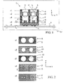
- FIG. 3 shows a schematic cross-sectional view of wafers for forming a wafer stack for manufacturing multiple modules as shown in FIG. 1 .
- a wafer refers to a substantially disk- or plate-like shaped item, its extension in one direction (z-direction or vertical direction) is small with respect to its extension in the other two directions (x- and y-directions or lateral directions).
- a (non-blank) wafer On a (non-blank) wafer, a plurality of similar structures or items can be arranged, or provided therein, for example, on a rectangular grid.
- a wafer can have openings or holes, and in some cases a wafer may be free of material in a predominant portion of its lateral area.
- a wafer may be made, for example, of a semiconductor material, a polymer material, a composite material comprising metals and polymers or polymers and glass materials.
- the wafers may comprise hardenable materials such as a thermally or UV-curable polymers.
- the diameter of a wafer is between 5 cm and 40 cm, and can be, for example between 10 cm and 31 cm.
- the wafer may be cylindrical with a diameter, for example, of 5.8, 10.16, 15.24, 20.32 or 30.48 cm (i.e. 2, 4, 6, 8 or 12 inches, one inch being about 2.54 cm).
- the wafer thickness can be, for example, between 0.2 mm and 10 mm, and in some cases, is between 0.4 mm and 6 mm.
- FIGS. 3 and 4 only show provisions for three modules 1, in some implementations there can be, in one wafer stack, provisions for at least ten modules in each lateral direction, and in some cases at least thirty or even fifty or more modules in each lateral direction.
- Examples of the dimensions of each of the wafers are: laterally at least 5 cm or 10 cm, and up to 30 cm or 40 cm or even 50 cm; and vertically (measured with no components arranged on substrate wafer PW) at least 0.2 mm or 0.4 mm or even 1 mm, and up to 6 mm or 10 mm or even 20 mm.
- the stack includes a substrate wafer PW, a spacer wafer SW, an optics wafer OW and a baffle wafer BW.
- Each wafer comprises a multitude of the corresponding members comprised in the corresponding module 1 (cf. FIGS. 1 and 2 ), arranged for example on a rectangular lattice, with a little distance from each other to facilitate a subsequent separation step.
- Substrate wafer PW can be, for example, a PCB assembly comprising a PCB of standard PCB materials, provided with solder balls 7 on the one side and with active optical components (e.g., members E and D) soldered to the other side.
- active optical components e.g., members E and D
- the latter can be placed on substrate wafer PW, for example, by pick-and-place using standard pick-and-place machines.
- the spacer wafer SW can help maintain the substrate wafer PW and the optics wafer OW at substantially a constant distance from one another.
- incorporating the spacer wafer SW into the wafer stack can enable higher imaging performance and complexity.
- the stacked wafer subsequently can be diced into individual micro-optics structures, resulting in multiple (e.g., thousands) of structures per wafer.
- each of the wafers PW, SW, OW, BW can be made substantially of a material that is substantially non-transparent for light detectable by detecting members D, except for transparent areas such as transparent portions t and transparent regions 3.
- the spacer wafer SW can be made of a UV- or thermally-curing epoxy (or other polymer) containing carbon black or other dark pigment,
- the carbon black is embedded in the epoxy (or other polymer).
- the amount of carbon black in the epoxy may depend on the particular application and may depend, for example, on the desired or required optical characteristics of the spacer wafer SW.
- the spacer wafer SW can be made of a UV or thermally curing epoxy containing at least 0.7% carbon black, although in some implementations a lower amount of carbon black can be sufficient.
- the optimal or desired percentage of carbon black in the epoxy for the spacer wafer SW may be adjusted, for example, depending on the lateral thickness of the wall 12.
- the wall thickness is about 200 ⁇ m
- the epoxy material contains about at least 0.8% carbon black.
- the foregoing composition can result in an absorption coefficient ( ⁇ ) of about 0.0295/ ⁇ m.
- the transmission T 10 ⁇ - ⁇ ⁇ d >for a wall portion 12 having a thickness d.
- the transmission (T) through the wall portion 12 is less than 0.00015%, which corresponds to an absorbance, or optical density, of about 5.8, where the absorbance represents a logarithmic ratio of the amount of radiation falling on a material to the amount of radiation transmitted through the material.
- the amount of carbon black is sufficiently high such that the transmission (T) of light through the wall portion 12 at the wavelength of light emitted by the emission member E is no greater than 0.1%.
- the amount of carbon black is sufficiently high such that the absorbance, or optical density, of the wall portion 12 at the wavelength of light emitted by the emission member E is at least 3.
- the separation member S has an absorption coefficient ( ⁇ ) of at least 0.015/ ⁇ m at the wavelength of light emitted by the light emitter for a thickness of about 200 ⁇ m for the wall 12.
- Various polymer materials e.g., epoxy resin, acrylate, polyurethane, or silicone materials
- the base material for the spacer wafer SW can be used as the base material for the spacer wafer SW, with the addition of one or more pigments or other adhesives to reduce the optical transmission characteristics of the spacer wafer at the wavelength(s) of interest (i.e., the wavelength(s) of light emitted by the LED or other emission member E).
- Examples of base materials for the spacer wafer SW include one or more of the following: EMCAST TM (e.g., 23xx, 24xx, 25xx and 2600 series), available from Electronic Materials, Inc.; MASTERBOND TM (e.g., UV15-7DC, UV1ODCTK) available from Master Bond Inc.; DELO-DUALBOND TM (e.g., AD VE 80342) available from DELO Industrial Adhesives; AC A1449, available from Addison Clear Wave; EPOTEK OG198-54, available from Epoxy Technology, Inc.; and LOCTITE 334, 392, 5091. Some of the foregoing materials are dual-curing (i.e., can be cured by UV light as well as thermally).
- EMCAST TM e.g., 23xx, 24xx, 25xx and 2600 series
- MASTERBOND TM e.g., UV15-7DC, UV1ODCTK
- DELO-DUALBOND TM e.g.,
- Carbon black or other pigments can be added to the base material to reduce the optical transmission characteristics of the spacer wafer SW at the wavelength(s) of interest.
- carbon black or another pigment can be added to the base polymer material in an amount that is sufficiently high such that the transmission (T) of light through the wall portion 12 at the wavelength of light emitted by the emission member E is no greater than 0.1%.
- the amount of the pigment is sufficiently high such that the absorbance, or optical density, of the wall portion 12 at the wavelength of light emitted by the emission member E is at least 3.
- the spacer wafers SW and baffle wafer BW, as well as at least a portion of optics wafer OW, can be fabricated, for example, by replication.
- Replication refers to a technique by means of which a given structure or a negative thereof is reproduced, e.g., etching, embossing, molding or vacuum injection.
- a structured surface is embossed into a liquid, viscous or plastically deformable material, then the material is hardened, e.g., by curing using ultraviolet radiation or heating, and then the structured surface is removed.
- a replica which in this case is a negative replica
- Suitable materials for replication are, for example, hardenable (e.g., curable) polymer materials or other replication materials, i.e. materials which are transformable in a hardening or solidification step (e.g., a curing step) from a liquid, viscous or plastically deformable state into a solid state.
- hardenable e.g., curable
- solidification step e.g., a curing step
- the wafer-level replication process thus can be implemented, for example, by precisely dispensing droplets of application-specific liquid polymer onto a wafer.
- the polymer then is embossed with a mold and cured on the wafer using ultraviolet light to harden it.
- the wafer then is separated from the mold. This process can be repeated on the other side of the wafer with micro-meter alignment accuracy.
- the replication material can be confined between a tool and the surface of the substrate as described in U.S. Pat. No. 7,704,418 .
- Suitable replication techniques for fabricating the spacer wafer SW are disclosed, for example, in U.S. Published Patent Application No. 2011/0039048 A1 , and in U.S. Provisional Application No. 61/746,347 .
- the spacer wafer SW can be fabricated such that its thickness at the edges exceeds the thickness of the spacer wafer at surface locations around the edges. In this way, the edges are elevated with regard to the average thickness of the spacer. For example, if the spacer wafer SW itself typically has a thickness of 100 to 1500 microns ( ⁇ m), the elevation of the edges with regard to the surrounding surface may be around 1-10 ⁇ m.
- the replicated elements e.g. spacer wafer SW, optics wafer OW, and substrate wafer PW
- the replicated elements are thermally stable and can withstand heat processes, such as reflow processes, where temperatures can reach, for example, up to about 260° C.
- Thermally stable elements substantially retain their general shape and do not decompose at relatively high operating temperatures. This characteristic of the replicated elements is generally referred to as "reflowability."
- the materials used to fabricate the thermally stable elements can include, for example, thermosetting polymers or thermoplastic polymers.
- the reflowable elements satisfy GR-468 CORE environmental tests including thermal cycling of 1000 times between -40° C. and +85° C., and 1000 hours at +85° C. temperature and 85% relative humidity.
- the spacer wafer SW can be a thermally-curing epoxy, formed from an epoxy resin and hardener, which in some implementations also contains carbon black.
- the thermal stability of such epoxy compounds depends primarily on the chemical structure of the epoxy resin and on the type of hardener.
- the glass transition temperatures of an epoxy compound can vary within the range of about 100 to about 270° C.
- the replicated elements also can be formed from thermally stable, ultraviolet (UV)-curable epoxies or other polymer materials.
- the replicated elements can be formed using materials that are "dual-curable.” That is, the materials can be cured using either heat (thermally curable) or ultraviolet light (UV-curable), depending on which of the two curing methods is employed.
- thermally stable curable polymers examples include one or more of the following: EMCAST TM (e.g., 23xx, 24xx, 25xx and 2600 series), available from Electronic Materials, Inc.; MASTERBOND TM epoxies (e.g., UV15-7DC and UV1ODCTK) available from Master Bond Inc.; DELO-DUALBOND TM (e.g., AD VE 80342) material available from DELO Industrial Adhesives; AC A1449, available from Addison Clear Wave; EPOTEK OG198-54 epoxy, available from Epoxy Technology, Inc.; and/or LOCTITE 334, 392, and 5091 series materials.
- EMCAST TM e.g., 23xx, 24xx, 25xx and 2600 series
- MASTERBOND TM epoxies e.g., UV15-7DC and UV1ODCTK
- DELO-DUALBOND TM e.g., AD VE 80342
- DELO Industrial Adhesives
- Examples of other materials include epoxies having functional amino silanes and a copolymer of aminopropylmethyl dimethyl siloxane in definite ratios.
- the use of silicon compounds in curable epoxies can, in some implementations, enhance the thermal stability, chemical resistance and corrosion resistance of the epoxy, whereas the use of silane bearing trimethoxy groups may provide better adhesion properties.
- the thermal stability of curable epoxies or other polymers can be enhanced by using ring compounds as curing agents.
- the thermal stability of epoxy resins made from bisphenol A can be enhanced by using aromatic amines and anhydrides, novolaks, bismaleimides (e.g., di-(p-maleimidophenyl) methane), and imidazole derivatives, among others. Additional resin and curing agent combinations can be used to enhance thermal stability as well.
- the materials for the lenses L also can be made of suitable reflowable material, in which the reflowable material is transparent for light detectable by a detecting member D.
- suitable material for lenses L can include, for example, hardenable (e.g., curable) polymer materials or materials that are transformed in a hardening (e.g., curing) step from a liquid, viscous or plastically deformable state into a solid state.
- curing of the lens material is achieved through the application of heat, UV light or a chemical additive to the polymer material.
- Other polymer materials that can be used to form the lenses include, for example, one or more of the following: THREEBOND TM 3078A, 3078B, or 3078C series epoxies, available from ThreeBond Co., Ltd.; DELO-KATIOBOND TM AD VE 18499 epoxy and DELO-PHOTOBOND TM epoxy (e.g., GB368 and 19923 series), each of which is available from DELO Industrial Adhesives; EPOTEK TM epoxies (e.g., 90-172-4, 90-174-3, 100-24-3, or OG142-13 series epoxies); Kyoritsu XLM-05 or XRC 9-2 series epoxies, available from Kyoritsu Chemical & Co., Ltd.; MRT Ormo
- opticals wafer OW replication or molding may be used for obtaining the non-transparent portions (e.g., blocking portions b). It also is possible to provide holes, where transparent portions t are supposed to be, by drilling or by etching. Subsequently, a soobtained precursor wafer is provided with lens members L, so as to yield optics wafer OW. This may be accomplished by means of replication, e.g., forming lens members L as unitary parts. The lens members L, however, also can be manufactured starting from a semi-finished part being a wafer comprising transparent elements 6 within holes by which transparent regions 3 are defined.
- Such a semi-finished part is can be a flat disk-like wafer having no holes penetrating the wafer in the transparent regions 3 and having virtually no or only shallow surface corrugations, such surface corrugations usually being concave, i.e. not extending beyond the wafer surface as described by the blocking portions b.
- the wafer can be placed on a flat support plate, e.g., made of a silicone.
- the dispensed material is cured, e.g., by heat or UV radiation, so as to obtain hardened transparent material.
- Convex meniscuses possibly formed this way can be flattened by polishing, so as to obtain a transparent element 6 having parallel surfaces adjusted to the wafer thickness. Then, by means of replication, lens elements 5 are applied to one or both sides (top and button sides) of wafer OW. In case of concave meniscuses of the transparent elements, the replication can take place on these, wherein the amount of applied replication material may be adjusted accordingly.
- a combined optics wafer which incorporates the features and functionalities of the optics wafer OW as well as the spacer wafer SW and/or the baffle wafer BW.
- Producing such a combined optics wafer can be accomplished using a particular precursor wafer and, manufactured based thereon, a particular semi-finished part.
- a precursor wafer and semi-finished part respectively, has at least one structured surface, usually having protrusions extending vertically beyond at least one of the two surfaces of transparent elements to be provided in precursor wafer and present in the semi-finished part, respectively.
- FIG. 5 an example of a semi-finished part ow' with one structured surface is schematically illustrated.
- the semi-finished part can be used for manufacturing a module shown in FIG. 1 .
- wafers OW and SW or wafers OW and BW, or wafers OW and SW and BW in FIG. 4 as one single part, a combined optics wafer is provided for manufacturing a module according to FIG. 1 .
- a hole may be formed in the substrate wafer PW, in which the hole extends through a thickness of the substrate wafer PW, to provide venting during the reflow process in order to release pressure build-up.
- the hole can be formed in the substrate wafer PW through drilling or an etching process.
- FIG. 4 shows a cross-sectional view of a wafer stack 2 for manufacturing multiple modules 1 as shown in FIG. 1 .
- the thin dashed rectangles indicate where separation takes place, e.g., by means of using a dicing saw.
- module 1 is a proximity sensor module.
- the techniques described above allow multiple modules to be fabricated at the same time using a wafer-level manufacturing process.
- the packaged module 1 can be incorporated into and operably connected to a wide range of devices, such as a portable electronic device, a hand-held portable electronic device, a personal computing device, a camera, an audio or video playback device, a laptop computer, or a personal digital assistant.
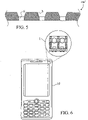
- a particular example of an application for the proximity sensor module 1 is in a mobile phone 10 (see FIG. 6 ).
- the proximity sensor module 1 can be used to detect that a mobile phone is next to the user's ear or face so that the phone's display can be dimmed or deactivated automatically when the display is not being used, thereby extending the life of the phone's battery.
- some implementations of the mobile phone 10 include a processor 52, memory 64, an input/output device such as a display 54, a communication interface 66, and a transceiver 68, among other components.
- the various components can be interconnected using various buses, and several of the components may be mounted on a common motherboard or in other manners as appropriate.
- the proximity sensor module I also can be interconnected to other components in the device 10 and, in some implementations, can be mounted on the common motherboard with some of the other components.
Landscapes
- Engineering & Computer Science (AREA)
- Physics & Mathematics (AREA)
- General Physics & Mathematics (AREA)
- Microelectronics & Electronic Packaging (AREA)
- Remote Sensing (AREA)
- Radar, Positioning & Navigation (AREA)
- Computer Networks & Wireless Communication (AREA)
- Electromagnetism (AREA)
- Condensed Matter Physics & Semiconductors (AREA)
- Power Engineering (AREA)
- Computer Hardware Design (AREA)
- Manufacturing & Machinery (AREA)
- General Life Sciences & Earth Sciences (AREA)
- Geophysics (AREA)
- Life Sciences & Earth Sciences (AREA)
- Ophthalmology & Optometry (AREA)
- Mechanical Engineering (AREA)
- Health & Medical Sciences (AREA)
- Spectroscopy & Molecular Physics (AREA)
- Led Device Packages (AREA)
- Light Receiving Elements (AREA)
- Geophysics And Detection Of Objects (AREA)
- Photo Coupler, Interrupter, Optical-To-Optical Conversion Devices (AREA)
- Solid State Image Pick-Up Elements (AREA)
- Semiconductor Lasers (AREA)
Applications Claiming Priority (3)
| Application Number | Priority Date | Filing Date | Title |
|---|---|---|---|
| US201261620587P | 2012-04-05 | 2012-04-05 | |
| US13/804,303 US9063005B2 (en) | 2012-04-05 | 2013-03-14 | Reflowable opto-electronic module |
| PCT/SG2013/000132 WO2013151508A1 (en) | 2012-04-05 | 2013-04-03 | Reflowable opto-electronic module |
Publications (3)
| Publication Number | Publication Date |
|---|---|
| EP2834844A1 EP2834844A1 (en) | 2015-02-11 |
| EP2834844A4 EP2834844A4 (en) | 2015-10-07 |
| EP2834844B1 true EP2834844B1 (en) | 2022-07-13 |
Family
ID=49292701
Family Applications (1)
| Application Number | Title | Priority Date | Filing Date |
|---|---|---|---|
| EP13772963.8A Active EP2834844B1 (en) | 2012-04-05 | 2013-04-03 | Method of fabricating a plurality of optical proximity sensor modules |
Country Status (8)
Families Citing this family (29)
| Publication number | Priority date | Publication date | Assignee | Title |
|---|---|---|---|---|
| TWI467777B (zh) * | 2012-06-06 | 2015-01-01 | Pixart Imaging Inc | 光學裝置之封裝結構 |
| CN104122541B (zh) * | 2013-04-28 | 2016-08-17 | 意法半导体研发(深圳)有限公司 | 具有互连层的接近检测器设备及相关方法 |
| CN104347644B (zh) * | 2013-07-25 | 2018-06-19 | 意法半导体研发(深圳)有限公司 | 具有透镜组件的图像检测器及相关方法 |
| TW201505131A (zh) * | 2013-07-25 | 2015-02-01 | Lingsen Precision Ind Ltd | 光學模組的封裝結構 |
| US9354111B2 (en) * | 2013-10-18 | 2016-05-31 | Maxim Integrated Products, Inc. | Wafer level lens in package |
| JP5907200B2 (ja) * | 2014-03-18 | 2016-04-26 | セイコーエプソン株式会社 | 光検出ユニット及び生体情報検出装置 |
| US9711552B2 (en) * | 2014-08-19 | 2017-07-18 | Heptagon Micro Optics Pte. Ltd. | Optoelectronic modules having a silicon substrate, and fabrication methods for such modules |
| CN106817910B (zh) * | 2014-10-14 | 2019-12-13 | 赫普塔冈微光有限公司 | 光学元件堆叠组件 |
| CN105679753B (zh) * | 2014-11-20 | 2018-05-08 | 日月光半导体制造股份有限公司 | 光学模块、其制造方法及电子装置 |
| CN105789197B (zh) * | 2014-12-25 | 2019-03-15 | 日月光半导体制造股份有限公司 | 光学模块、其制造方法以及具有光学模块的电子装置 |
| US9696199B2 (en) * | 2015-02-13 | 2017-07-04 | Taiwan Biophotonic Corporation | Optical sensor |
| EP3104190B1 (en) * | 2015-06-08 | 2024-04-17 | ams AG | Optical sensor arrangement |
| US10663698B2 (en) | 2015-08-27 | 2020-05-26 | Ams Sensors Singapore Pte. Ltd. | Optical assemblies including a spacer adhering directly to a substrate |
| WO2017082820A1 (en) | 2015-11-12 | 2017-05-18 | Heptagon Micro Optics Pte. Ltd. | Optical element stack assemblies |
| US10551596B2 (en) | 2016-06-29 | 2020-02-04 | Ams Sensors Singapore Pte. Ltd. | Optical and optoelectronic assemblies including micro-spacers, and methods of manufacturing the same |
| US10243111B2 (en) | 2016-06-29 | 2019-03-26 | Ams Sensors Singapore Pte. Ltd. | Optoelectronic device subassemblies and methods of manufacturing the same |
| US10459189B2 (en) | 2016-10-05 | 2019-10-29 | Omnivision Technologies, Inc. | Lens barrel, lens-barrel wafer, and associated method |
| CN106453723B (zh) * | 2016-12-06 | 2022-10-21 | Oppo广东移动通信有限公司 | 传感器组件及终端 |
| CN106847802B (zh) * | 2016-12-29 | 2019-09-24 | 矽力杰半导体技术(杭州)有限公司 | 光学传感器封装组件及其制作方法和电子设备 |
| US10461744B2 (en) | 2017-09-21 | 2019-10-29 | Google Llc | Proximity sensor connection mechanism |
| US11585901B2 (en) * | 2017-11-15 | 2023-02-21 | Veoneer Us, Llc | Scanning lidar system and method with spatial filtering for reduction of ambient light |
| US10859776B2 (en) * | 2018-04-06 | 2020-12-08 | The Regents Of The University Of California | Optical-electrical interposers |
| CN109461662B (zh) * | 2018-09-28 | 2020-06-02 | 深圳赛意法微电子有限公司 | 多点近距离感应器的封装方法 |
| DE112020000917T5 (de) * | 2019-02-25 | 2021-11-04 | Ams Sensors Singapore Pte. Ltd. | Herstellung von optischen diffusoren und optische diffusoren |
| US20220216353A1 (en) * | 2019-04-08 | 2022-07-07 | Ams Ag | Optical sensor including integrated diffuser |
| CN112497884A (zh) * | 2020-11-27 | 2021-03-16 | 瑞昌荣联环保科技有限公司 | 一种亚克力板材覆膜机 |
| DE102020215033A1 (de) * | 2020-11-30 | 2022-06-02 | Robert Bosch Gesellschaft mit beschränkter Haftung | Laserdiodenvorrichtung |
| US12176220B2 (en) | 2020-12-15 | 2024-12-24 | Stmicroelectronics Pte Ltd | Optical sensor package and method of making an optical sensor package |
| DE102021132724A1 (de) * | 2021-12-10 | 2023-06-15 | Valeo Schalter Und Sensoren Gmbh | Optischer fahrzeug-umgebungssensor, fahrzeug und herstellungsverfahren |
Citations (1)
| Publication number | Priority date | Publication date | Assignee | Title |
|---|---|---|---|---|
| JP2010123620A (ja) * | 2008-11-17 | 2010-06-03 | Stanley Electric Co Ltd | 半導体装置の製造方法 |
Family Cites Families (23)
| Publication number | Priority date | Publication date | Assignee | Title |
|---|---|---|---|---|
| JPS61158606A (ja) * | 1984-12-28 | 1986-07-18 | 株式会社小糸製作所 | 照明装置 |
| JPH11289105A (ja) * | 1998-04-03 | 1999-10-19 | Citizen Electronics Co Ltd | フォトリフレクタとその製造方法 |
| US6710346B2 (en) * | 2001-08-02 | 2004-03-23 | International Business Machines Corporation | Active infrared presence sensor |
| JP2004163116A (ja) | 2002-11-08 | 2004-06-10 | Sanyo Electric Co Ltd | 反射型光センサ装置 |
| US20070216048A1 (en) | 2006-03-20 | 2007-09-20 | Heptagon Oy | Manufacturing optical elements |
| US20070284687A1 (en) | 2006-06-13 | 2007-12-13 | Rantala Juha T | Semiconductor optoelectronics devices |
| JP4720665B2 (ja) * | 2006-07-31 | 2011-07-13 | パナソニック電工株式会社 | Led照明器具 |
| CH713513B1 (fr) * | 2007-02-22 | 2018-08-31 | Em Microelectronic Marin Sa | Module optoélectronique muni d'au moins un circuit photorécepteur. |
| TWI382753B (zh) | 2007-12-17 | 2013-01-11 | Omnivision Tech Inc | 具有整合式閃光燈之可回銲相機模組 |
| US20090159200A1 (en) | 2007-12-19 | 2009-06-25 | Heptagon Oy | Spacer element and method for manufacturing a spacer element |
| US8092251B2 (en) * | 2007-12-29 | 2012-01-10 | Apple Inc. | Active electronic media device packaging |
| US8779361B2 (en) * | 2009-06-30 | 2014-07-15 | Avago Technologies General Ip (Singapore) Pte. Ltd. | Optical proximity sensor package with molded infrared light rejection barrier and infrared pass components |
| US8319170B2 (en) * | 2009-07-10 | 2012-11-27 | Motorola Mobility Llc | Method for adapting a pulse power mode of a proximity sensor |
| US8716665B2 (en) | 2009-09-10 | 2014-05-06 | Avago Technologies General Ip (Singapore) Pte. Ltd. | Compact optical proximity sensor with ball grid array and windowed substrate |
| US8097852B2 (en) | 2009-09-10 | 2012-01-17 | Avago Technologies Ecbu Ip (Singapore) Pte. Ltd. | Multiple transfer molded optical proximity sensor and corresponding method |
| US9733357B2 (en) * | 2009-11-23 | 2017-08-15 | Avago Technologies General Ip (Singapore) Pte. Ltd. | Infrared proximity sensor package with improved crosstalk isolation |
| US8742350B2 (en) | 2010-06-08 | 2014-06-03 | Avago Technologies General Ip (Singapore) Pte. Ltd. | Proximity sensor |
| US20130153755A1 (en) | 2010-08-03 | 2013-06-20 | Nokia Corporation | Optical Proximity Sensing |
| CN103620779B (zh) | 2011-07-19 | 2016-12-28 | 赫普塔冈微光有限公司 | 光电模块及其制造方法 |
| US8791489B2 (en) * | 2012-04-05 | 2014-07-29 | Heptagon Micro Optics Pte. Ltd. | Opto-electronic module |
| US8946620B2 (en) * | 2012-10-16 | 2015-02-03 | Avago Technologies General Ip (Singapore) Pte. Ltd. | Proximity sensor device with internal channeling section |
| DE102013202170B4 (de) * | 2013-02-11 | 2023-03-09 | Robert Bosch Gmbh | Optische Sensorchipvorrichtung und entsprechendes Herstellungsverfahren |
| TW201505132A (zh) * | 2013-07-25 | 2015-02-01 | Lingsen Precision Ind Ltd | 光學模組的封裝結構 |
-
2013
- 2013-03-14 US US13/804,303 patent/US9063005B2/en active Active
- 2013-04-03 TW TW102112207A patent/TWI553840B/zh active
- 2013-04-03 EP EP13772963.8A patent/EP2834844B1/en active Active
- 2013-04-03 TW TW105119341A patent/TWI584452B/zh active
- 2013-04-03 WO PCT/SG2013/000132 patent/WO2013151508A1/en active Application Filing
- 2013-04-03 CN CN201380018899.3A patent/CN104247020B/zh active Active
- 2013-04-03 JP JP2015504532A patent/JP2015519546A/ja active Pending
- 2013-04-03 SG SG11201405658XA patent/SG11201405658XA/en unknown
- 2013-04-03 KR KR1020147030935A patent/KR102125532B1/ko active Active
-
2015
- 2015-05-18 US US14/715,201 patent/US9516152B2/en active Active
-
2017
- 2017-02-24 JP JP2017033644A patent/JP6328813B2/ja active Active
Patent Citations (1)
| Publication number | Priority date | Publication date | Assignee | Title |
|---|---|---|---|---|
| JP2010123620A (ja) * | 2008-11-17 | 2010-06-03 | Stanley Electric Co Ltd | 半導体装置の製造方法 |
Also Published As
| Publication number | Publication date |
|---|---|
| TWI584452B (zh) | 2017-05-21 |
| US20130267273A1 (en) | 2013-10-10 |
| US9516152B2 (en) | 2016-12-06 |
| CN104247020B (zh) | 2018-04-24 |
| TWI553840B (zh) | 2016-10-11 |
| JP6328813B2 (ja) | 2018-05-23 |
| CN104247020A (zh) | 2014-12-24 |
| WO2013151508A1 (en) | 2013-10-10 |
| EP2834844A1 (en) | 2015-02-11 |
| KR20150010721A (ko) | 2015-01-28 |
| KR102125532B1 (ko) | 2020-06-24 |
| JP2017130668A (ja) | 2017-07-27 |
| US9063005B2 (en) | 2015-06-23 |
| JP2015519546A (ja) | 2015-07-09 |
| US20150249734A1 (en) | 2015-09-03 |
| EP2834844A4 (en) | 2015-10-07 |
| TW201349466A (zh) | 2013-12-01 |
| TW201635500A (zh) | 2016-10-01 |
| SG11201405658XA (en) | 2014-11-27 |
Similar Documents
| Publication | Publication Date | Title |
|---|---|---|
| EP2834844B1 (en) | Method of fabricating a plurality of optical proximity sensor modules | |
| US8975108B2 (en) | Opto-electronic module | |
| US9746349B2 (en) | Opto-electronic module including a non-transparent separation member between a light emitting element and a light detecting element | |
| US11005001B2 (en) | Opto-electronic modules and methods of manufacturing the same and appliances and devices comprising the same |
Legal Events
| Date | Code | Title | Description |
|---|---|---|---|
| PUAI | Public reference made under article 153(3) epc to a published international application that has entered the european phase |
Free format text: ORIGINAL CODE: 0009012 |
|
| 17P | Request for examination filed |
Effective date: 20141013 |
|
| AK | Designated contracting states |
Kind code of ref document: A1 Designated state(s): AL AT BE BG CH CY CZ DE DK EE ES FI FR GB GR HR HU IE IS IT LI LT LU LV MC MK MT NL NO PL PT RO RS SE SI SK SM TR |
|
| AX | Request for extension of the european patent |
Extension state: BA ME |
|
| DAX | Request for extension of the european patent (deleted) | ||
| RA4 | Supplementary search report drawn up and despatched (corrected) |
Effective date: 20150908 |
|
| RIC1 | Information provided on ipc code assigned before grant |
Ipc: H01L 31/00 20060101ALI20150902BHEP Ipc: G01S 17/02 20060101ALI20150902BHEP Ipc: H03K 17/94 20060101ALI20150902BHEP Ipc: G01J 1/02 20060101ALI20150902BHEP Ipc: H01L 25/065 20060101ALI20150902BHEP Ipc: H01L 27/14 20060101AFI20150902BHEP Ipc: H01L 31/12 20060101ALI20150902BHEP Ipc: G01S 17/48 20060101ALI20150902BHEP Ipc: G01S 7/481 20060101ALI20150902BHEP Ipc: H01L 25/16 20060101ALI20150902BHEP Ipc: G01V 8/12 20060101ALI20150902BHEP |
|
| 17Q | First examination report despatched |
Effective date: 20150924 |
|
| STAA | Information on the status of an ep patent application or granted ep patent |
Free format text: STATUS: EXAMINATION IS IN PROGRESS |
|
| STAA | Information on the status of an ep patent application or granted ep patent |
Free format text: STATUS: EXAMINATION IS IN PROGRESS |
|
| REG | Reference to a national code |
Ref country code: DE Ref legal event code: R079 Ref document number: 602013082067 Country of ref document: DE Free format text: PREVIOUS MAIN CLASS: H01L0027140000 Ipc: H01L0027146000 |
|
| RIC1 | Information provided on ipc code assigned before grant |
Ipc: G01S 7/481 20060101ALI20211222BHEP Ipc: H03K 17/94 20060101ALI20211222BHEP Ipc: H01L 25/16 20060101ALI20211222BHEP Ipc: G01J 1/02 20060101ALI20211222BHEP Ipc: G01V 8/12 20060101ALI20211222BHEP Ipc: G01S 17/04 20200101ALI20211222BHEP Ipc: B29D 11/00 20060101ALI20211222BHEP Ipc: H03K 17/945 20060101ALI20211222BHEP Ipc: H01L 27/146 20060101AFI20211222BHEP |
|
| GRAP | Despatch of communication of intention to grant a patent |
Free format text: ORIGINAL CODE: EPIDOSNIGR1 |
|
| STAA | Information on the status of an ep patent application or granted ep patent |
Free format text: STATUS: GRANT OF PATENT IS INTENDED |
|
| INTG | Intention to grant announced |
Effective date: 20220131 |
|
| RIN1 | Information on inventor provided before grant (corrected) |
Inventor name: BIETSCH, ALEXANDER Inventor name: RUDMANN, HARTMUT |
|
| GRAS | Grant fee paid |
Free format text: ORIGINAL CODE: EPIDOSNIGR3 |
|
| GRAA | (expected) grant |
Free format text: ORIGINAL CODE: 0009210 |
|
| STAA | Information on the status of an ep patent application or granted ep patent |
Free format text: STATUS: THE PATENT HAS BEEN GRANTED |
|
| AK | Designated contracting states |
Kind code of ref document: B1 Designated state(s): AL AT BE BG CH CY CZ DE DK EE ES FI FR GB GR HR HU IE IS IT LI LT LU LV MC MK MT NL NO PL PT RO RS SE SI SK SM TR |
|
| REG | Reference to a national code |
Ref country code: GB Ref legal event code: FG4D |
|
| REG | Reference to a national code |
Ref country code: CH Ref legal event code: EP |
|
| REG | Reference to a national code |
Ref country code: IE Ref legal event code: FG4D |
|
| REG | Reference to a national code |
Ref country code: DE Ref legal event code: R096 Ref document number: 602013082067 Country of ref document: DE |
|
| REG | Reference to a national code |
Ref country code: AT Ref legal event code: REF Ref document number: 1504716 Country of ref document: AT Kind code of ref document: T Effective date: 20220815 |
|
| REG | Reference to a national code |
Ref country code: LT Ref legal event code: MG9D |
|
| REG | Reference to a national code |
Ref country code: NL Ref legal event code: MP Effective date: 20220713 |
|
| PG25 | Lapsed in a contracting state [announced via postgrant information from national office to epo] |
Ref country code: SE Free format text: LAPSE BECAUSE OF FAILURE TO SUBMIT A TRANSLATION OF THE DESCRIPTION OR TO PAY THE FEE WITHIN THE PRESCRIBED TIME-LIMIT Effective date: 20220713 Ref country code: RS Free format text: LAPSE BECAUSE OF FAILURE TO SUBMIT A TRANSLATION OF THE DESCRIPTION OR TO PAY THE FEE WITHIN THE PRESCRIBED TIME-LIMIT Effective date: 20220713 Ref country code: PT Free format text: LAPSE BECAUSE OF FAILURE TO SUBMIT A TRANSLATION OF THE DESCRIPTION OR TO PAY THE FEE WITHIN THE PRESCRIBED TIME-LIMIT Effective date: 20221114 Ref country code: NO Free format text: LAPSE BECAUSE OF FAILURE TO SUBMIT A TRANSLATION OF THE DESCRIPTION OR TO PAY THE FEE WITHIN THE PRESCRIBED TIME-LIMIT Effective date: 20221013 Ref country code: NL Free format text: LAPSE BECAUSE OF FAILURE TO SUBMIT A TRANSLATION OF THE DESCRIPTION OR TO PAY THE FEE WITHIN THE PRESCRIBED TIME-LIMIT Effective date: 20220713 Ref country code: LV Free format text: LAPSE BECAUSE OF FAILURE TO SUBMIT A TRANSLATION OF THE DESCRIPTION OR TO PAY THE FEE WITHIN THE PRESCRIBED TIME-LIMIT Effective date: 20220713 Ref country code: LT Free format text: LAPSE BECAUSE OF FAILURE TO SUBMIT A TRANSLATION OF THE DESCRIPTION OR TO PAY THE FEE WITHIN THE PRESCRIBED TIME-LIMIT Effective date: 20220713 Ref country code: FI Free format text: LAPSE BECAUSE OF FAILURE TO SUBMIT A TRANSLATION OF THE DESCRIPTION OR TO PAY THE FEE WITHIN THE PRESCRIBED TIME-LIMIT Effective date: 20220713 Ref country code: ES Free format text: LAPSE BECAUSE OF FAILURE TO SUBMIT A TRANSLATION OF THE DESCRIPTION OR TO PAY THE FEE WITHIN THE PRESCRIBED TIME-LIMIT Effective date: 20220713 |
|
| REG | Reference to a national code |
Ref country code: AT Ref legal event code: MK05 Ref document number: 1504716 Country of ref document: AT Kind code of ref document: T Effective date: 20220713 |
|
| PG25 | Lapsed in a contracting state [announced via postgrant information from national office to epo] |
Ref country code: PL Free format text: LAPSE BECAUSE OF FAILURE TO SUBMIT A TRANSLATION OF THE DESCRIPTION OR TO PAY THE FEE WITHIN THE PRESCRIBED TIME-LIMIT Effective date: 20220713 Ref country code: IS Free format text: LAPSE BECAUSE OF FAILURE TO SUBMIT A TRANSLATION OF THE DESCRIPTION OR TO PAY THE FEE WITHIN THE PRESCRIBED TIME-LIMIT Effective date: 20221113 Ref country code: HR Free format text: LAPSE BECAUSE OF FAILURE TO SUBMIT A TRANSLATION OF THE DESCRIPTION OR TO PAY THE FEE WITHIN THE PRESCRIBED TIME-LIMIT Effective date: 20220713 Ref country code: GR Free format text: LAPSE BECAUSE OF FAILURE TO SUBMIT A TRANSLATION OF THE DESCRIPTION OR TO PAY THE FEE WITHIN THE PRESCRIBED TIME-LIMIT Effective date: 20221014 |
|
| REG | Reference to a national code |
Ref country code: DE Ref legal event code: R097 Ref document number: 602013082067 Country of ref document: DE |
|
| PG25 | Lapsed in a contracting state [announced via postgrant information from national office to epo] |
Ref country code: SM Free format text: LAPSE BECAUSE OF FAILURE TO SUBMIT A TRANSLATION OF THE DESCRIPTION OR TO PAY THE FEE WITHIN THE PRESCRIBED TIME-LIMIT Effective date: 20220713 Ref country code: RO Free format text: LAPSE BECAUSE OF FAILURE TO SUBMIT A TRANSLATION OF THE DESCRIPTION OR TO PAY THE FEE WITHIN THE PRESCRIBED TIME-LIMIT Effective date: 20220713 Ref country code: DK Free format text: LAPSE BECAUSE OF FAILURE TO SUBMIT A TRANSLATION OF THE DESCRIPTION OR TO PAY THE FEE WITHIN THE PRESCRIBED TIME-LIMIT Effective date: 20220713 Ref country code: CZ Free format text: LAPSE BECAUSE OF FAILURE TO SUBMIT A TRANSLATION OF THE DESCRIPTION OR TO PAY THE FEE WITHIN THE PRESCRIBED TIME-LIMIT Effective date: 20220713 Ref country code: AT Free format text: LAPSE BECAUSE OF FAILURE TO SUBMIT A TRANSLATION OF THE DESCRIPTION OR TO PAY THE FEE WITHIN THE PRESCRIBED TIME-LIMIT Effective date: 20220713 |
|
| PLBE | No opposition filed within time limit |
Free format text: ORIGINAL CODE: 0009261 |
|
| STAA | Information on the status of an ep patent application or granted ep patent |
Free format text: STATUS: NO OPPOSITION FILED WITHIN TIME LIMIT |
|
| PG25 | Lapsed in a contracting state [announced via postgrant information from national office to epo] |
Ref country code: SK Free format text: LAPSE BECAUSE OF FAILURE TO SUBMIT A TRANSLATION OF THE DESCRIPTION OR TO PAY THE FEE WITHIN THE PRESCRIBED TIME-LIMIT Effective date: 20220713 Ref country code: EE Free format text: LAPSE BECAUSE OF FAILURE TO SUBMIT A TRANSLATION OF THE DESCRIPTION OR TO PAY THE FEE WITHIN THE PRESCRIBED TIME-LIMIT Effective date: 20220713 |
|
| 26N | No opposition filed |
Effective date: 20230414 |
|
| PG25 | Lapsed in a contracting state [announced via postgrant information from national office to epo] |
Ref country code: AL Free format text: LAPSE BECAUSE OF FAILURE TO SUBMIT A TRANSLATION OF THE DESCRIPTION OR TO PAY THE FEE WITHIN THE PRESCRIBED TIME-LIMIT Effective date: 20220713 |
|
| PG25 | Lapsed in a contracting state [announced via postgrant information from national office to epo] |
Ref country code: SI Free format text: LAPSE BECAUSE OF FAILURE TO SUBMIT A TRANSLATION OF THE DESCRIPTION OR TO PAY THE FEE WITHIN THE PRESCRIBED TIME-LIMIT Effective date: 20220713 |
|
| P01 | Opt-out of the competence of the unified patent court (upc) registered |
Effective date: 20230825 |
|
| REG | Reference to a national code |
Ref country code: CH Ref legal event code: PL |
|
| GBPC | Gb: european patent ceased through non-payment of renewal fee |
Effective date: 20230403 |
|
| PG25 | Lapsed in a contracting state [announced via postgrant information from national office to epo] |
Ref country code: LU Free format text: LAPSE BECAUSE OF NON-PAYMENT OF DUE FEES Effective date: 20230403 |
|
| REG | Reference to a national code |
Ref country code: BE Ref legal event code: MM Effective date: 20230430 |
|
| PG25 | Lapsed in a contracting state [announced via postgrant information from national office to epo] |
Ref country code: MC Free format text: LAPSE BECAUSE OF FAILURE TO SUBMIT A TRANSLATION OF THE DESCRIPTION OR TO PAY THE FEE WITHIN THE PRESCRIBED TIME-LIMIT Effective date: 20220713 |
|
| PG25 | Lapsed in a contracting state [announced via postgrant information from national office to epo] |
Ref country code: GB Free format text: LAPSE BECAUSE OF NON-PAYMENT OF DUE FEES Effective date: 20230403 |
|
| PG25 | Lapsed in a contracting state [announced via postgrant information from national office to epo] |
Ref country code: MC Free format text: LAPSE BECAUSE OF FAILURE TO SUBMIT A TRANSLATION OF THE DESCRIPTION OR TO PAY THE FEE WITHIN THE PRESCRIBED TIME-LIMIT Effective date: 20220713 Ref country code: LI Free format text: LAPSE BECAUSE OF NON-PAYMENT OF DUE FEES Effective date: 20230430 Ref country code: IT Free format text: LAPSE BECAUSE OF FAILURE TO SUBMIT A TRANSLATION OF THE DESCRIPTION OR TO PAY THE FEE WITHIN THE PRESCRIBED TIME-LIMIT Effective date: 20220713 Ref country code: GB Free format text: LAPSE BECAUSE OF NON-PAYMENT OF DUE FEES Effective date: 20230403 Ref country code: FR Free format text: LAPSE BECAUSE OF NON-PAYMENT OF DUE FEES Effective date: 20230430 Ref country code: CH Free format text: LAPSE BECAUSE OF NON-PAYMENT OF DUE FEES Effective date: 20230430 |
|
| REG | Reference to a national code |
Ref country code: IE Ref legal event code: MM4A |
|
| PG25 | Lapsed in a contracting state [announced via postgrant information from national office to epo] |
Ref country code: BE Free format text: LAPSE BECAUSE OF NON-PAYMENT OF DUE FEES Effective date: 20230430 |
|
| PG25 | Lapsed in a contracting state [announced via postgrant information from national office to epo] |
Ref country code: IE Free format text: LAPSE BECAUSE OF NON-PAYMENT OF DUE FEES Effective date: 20230403 |
|
| PG25 | Lapsed in a contracting state [announced via postgrant information from national office to epo] |
Ref country code: IE Free format text: LAPSE BECAUSE OF NON-PAYMENT OF DUE FEES Effective date: 20230403 |
|
| REG | Reference to a national code |
Ref country code: DE Ref legal event code: R081 Ref document number: 602013082067 Country of ref document: DE Owner name: AMS-OSRAM ASIA PACIFIC PTE. LTD., SG Free format text: FORMER OWNER: HEPTAGON MICRO OPTICS PTE. LTD., SINGAPORE, SG |
|
| PG25 | Lapsed in a contracting state [announced via postgrant information from national office to epo] |
Ref country code: BG Free format text: LAPSE BECAUSE OF FAILURE TO SUBMIT A TRANSLATION OF THE DESCRIPTION OR TO PAY THE FEE WITHIN THE PRESCRIBED TIME-LIMIT Effective date: 20220713 |
|
| REG | Reference to a national code |
Ref country code: DE Ref legal event code: R079 Ref document number: 602013082067 Country of ref document: DE Free format text: PREVIOUS MAIN CLASS: H01L0027146000 Ipc: H10F0039180000 |
|
| PG25 | Lapsed in a contracting state [announced via postgrant information from national office to epo] |
Ref country code: BG Free format text: LAPSE BECAUSE OF FAILURE TO SUBMIT A TRANSLATION OF THE DESCRIPTION OR TO PAY THE FEE WITHIN THE PRESCRIBED TIME-LIMIT Effective date: 20220713 |
|
| PGFP | Annual fee paid to national office [announced via postgrant information from national office to epo] |
Ref country code: DE Payment date: 20250422 Year of fee payment: 13 |
|
| PG25 | Lapsed in a contracting state [announced via postgrant information from national office to epo] |
Ref country code: CY Free format text: LAPSE BECAUSE OF FAILURE TO SUBMIT A TRANSLATION OF THE DESCRIPTION OR TO PAY THE FEE WITHIN THE PRESCRIBED TIME-LIMIT; INVALID AB INITIO Effective date: 20130403 |
|
| PG25 | Lapsed in a contracting state [announced via postgrant information from national office to epo] |
Ref country code: HU Free format text: LAPSE BECAUSE OF FAILURE TO SUBMIT A TRANSLATION OF THE DESCRIPTION OR TO PAY THE FEE WITHIN THE PRESCRIBED TIME-LIMIT; INVALID AB INITIO Effective date: 20130403 |