US10859776B2 - Optical-electrical interposers - Google Patents
Optical-electrical interposers Download PDFInfo
- Publication number
- US10859776B2 US10859776B2 US16/375,667 US201916375667A US10859776B2 US 10859776 B2 US10859776 B2 US 10859776B2 US 201916375667 A US201916375667 A US 201916375667A US 10859776 B2 US10859776 B2 US 10859776B2
- Authority
- US
- United States
- Prior art keywords
- optical
- optical interposer
- pcb
- interposer
- connection elements
- Prior art date
- Legal status (The legal status is an assumption and is not a legal conclusion. Google has not performed a legal analysis and makes no representation as to the accuracy of the status listed.)
- Active, expires
Links
- 230000003287 optical effect Effects 0.000 claims abstract description 165
- 238000000034 method Methods 0.000 claims abstract description 38
- 230000010354 integration Effects 0.000 claims abstract description 24
- 229910000679 solder Inorganic materials 0.000 claims description 23
- 238000004891 communication Methods 0.000 claims description 13
- 230000015654 memory Effects 0.000 claims description 8
- RYGMFSIKBFXOCR-UHFFFAOYSA-N Copper Chemical compound [Cu] RYGMFSIKBFXOCR-UHFFFAOYSA-N 0.000 claims description 5
- 229910052802 copper Inorganic materials 0.000 claims description 5
- 239000010949 copper Substances 0.000 claims description 5
- 230000008878 coupling Effects 0.000 claims description 5
- 238000010168 coupling process Methods 0.000 claims description 5
- 238000005859 coupling reaction Methods 0.000 claims description 5
- 238000009792 diffusion process Methods 0.000 claims description 5
- 239000002184 metal Substances 0.000 claims description 5
- 229910052751 metal Inorganic materials 0.000 claims description 5
- 229920000642 polymer Polymers 0.000 claims description 4
- 230000008569 process Effects 0.000 description 11
- XUIMIQQOPSSXEZ-UHFFFAOYSA-N Silicon Chemical compound [Si] XUIMIQQOPSSXEZ-UHFFFAOYSA-N 0.000 description 7
- 229910052710 silicon Inorganic materials 0.000 description 7
- 239000010703 silicon Substances 0.000 description 7
- 238000003860 storage Methods 0.000 description 6
- VYPSYNLAJGMNEJ-UHFFFAOYSA-N Silicium dioxide Chemical compound O=[Si]=O VYPSYNLAJGMNEJ-UHFFFAOYSA-N 0.000 description 4
- 238000013461 design Methods 0.000 description 4
- 238000013459 approach Methods 0.000 description 3
- 238000004519 manufacturing process Methods 0.000 description 3
- 238000012986 modification Methods 0.000 description 3
- 230000004048 modification Effects 0.000 description 3
- 238000005516 engineering process Methods 0.000 description 2
- 230000005291 magnetic effect Effects 0.000 description 2
- 230000003071 parasitic effect Effects 0.000 description 2
- 239000000377 silicon dioxide Substances 0.000 description 2
- 229910052581 Si3N4 Inorganic materials 0.000 description 1
- 238000003491 array Methods 0.000 description 1
- 230000000712 assembly Effects 0.000 description 1
- 238000000429 assembly Methods 0.000 description 1
- 229910052681 coesite Inorganic materials 0.000 description 1
- 229910052906 cristobalite Inorganic materials 0.000 description 1
- 230000002500 effect on skin Effects 0.000 description 1
- 230000000694 effects Effects 0.000 description 1
- 230000006870 function Effects 0.000 description 1
- 238000010348 incorporation Methods 0.000 description 1
- 238000003475 lamination Methods 0.000 description 1
- 230000013011 mating Effects 0.000 description 1
- 150000003071 polychlorinated biphenyls Chemical class 0.000 description 1
- 238000012545 processing Methods 0.000 description 1
- 238000011084 recovery Methods 0.000 description 1
- 238000004088 simulation Methods 0.000 description 1
- 229910052682 stishovite Inorganic materials 0.000 description 1
- 229910052905 tridymite Inorganic materials 0.000 description 1
Images


Classifications
-
- H—ELECTRICITY
- H01—ELECTRIC ELEMENTS
- H01L—SEMICONDUCTOR DEVICES NOT COVERED BY CLASS H10
- H01L25/00—Assemblies consisting of a plurality of individual semiconductor or other solid state devices ; Multistep manufacturing processes thereof
- H01L25/03—Assemblies consisting of a plurality of individual semiconductor or other solid state devices ; Multistep manufacturing processes thereof all the devices being of a type provided for in the same subgroup of groups H01L27/00 - H01L33/00, or in a single subclass of H10K, H10N, e.g. assemblies of rectifier diodes
- H01L25/04—Assemblies consisting of a plurality of individual semiconductor or other solid state devices ; Multistep manufacturing processes thereof all the devices being of a type provided for in the same subgroup of groups H01L27/00 - H01L33/00, or in a single subclass of H10K, H10N, e.g. assemblies of rectifier diodes the devices not having separate containers
-
- G—PHYSICS
- G02—OPTICS
- G02B—OPTICAL ELEMENTS, SYSTEMS OR APPARATUS
- G02B6/00—Light guides; Structural details of arrangements comprising light guides and other optical elements, e.g. couplings
- G02B6/10—Light guides; Structural details of arrangements comprising light guides and other optical elements, e.g. couplings of the optical waveguide type
- G02B6/12—Light guides; Structural details of arrangements comprising light guides and other optical elements, e.g. couplings of the optical waveguide type of the integrated circuit kind
- G02B6/122—Basic optical elements, e.g. light-guiding paths
- G02B6/1228—Tapered waveguides, e.g. integrated spot-size transformers
-
- G—PHYSICS
- G02—OPTICS
- G02B—OPTICAL ELEMENTS, SYSTEMS OR APPARATUS
- G02B6/00—Light guides; Structural details of arrangements comprising light guides and other optical elements, e.g. couplings
- G02B6/24—Coupling light guides
- G02B6/42—Coupling light guides with opto-electronic elements
- G02B6/4201—Packages, e.g. shape, construction, internal or external details
- G02B6/4219—Mechanical fixtures for holding or positioning the elements relative to each other in the couplings; Alignment methods for the elements, e.g. measuring or observing methods especially used therefor
- G02B6/4228—Passive alignment, i.e. without a detection of the degree of coupling or the position of the elements
- G02B6/4232—Passive alignment, i.e. without a detection of the degree of coupling or the position of the elements using the surface tension of fluid solder to align the elements, e.g. solder bump techniques
-
- G—PHYSICS
- G02—OPTICS
- G02B—OPTICAL ELEMENTS, SYSTEMS OR APPARATUS
- G02B6/00—Light guides; Structural details of arrangements comprising light guides and other optical elements, e.g. couplings
- G02B6/24—Coupling light guides
- G02B6/42—Coupling light guides with opto-electronic elements
- G02B6/4201—Packages, e.g. shape, construction, internal or external details
- G02B6/4219—Mechanical fixtures for holding or positioning the elements relative to each other in the couplings; Alignment methods for the elements, e.g. measuring or observing methods especially used therefor
- G02B6/4236—Fixing or mounting methods of the aligned elements
- G02B6/4238—Soldering
-
- G—PHYSICS
- G02—OPTICS
- G02B—OPTICAL ELEMENTS, SYSTEMS OR APPARATUS
- G02B6/00—Light guides; Structural details of arrangements comprising light guides and other optical elements, e.g. couplings
- G02B6/24—Coupling light guides
- G02B6/42—Coupling light guides with opto-electronic elements
- G02B6/4201—Packages, e.g. shape, construction, internal or external details
- G02B6/4219—Mechanical fixtures for holding or positioning the elements relative to each other in the couplings; Alignment methods for the elements, e.g. measuring or observing methods especially used therefor
- G02B6/4236—Fixing or mounting methods of the aligned elements
- G02B6/4245—Mounting of the opto-electronic elements
-
- G—PHYSICS
- G02—OPTICS
- G02B—OPTICAL ELEMENTS, SYSTEMS OR APPARATUS
- G02B6/00—Light guides; Structural details of arrangements comprising light guides and other optical elements, e.g. couplings
- G02B6/24—Coupling light guides
- G02B6/42—Coupling light guides with opto-electronic elements
- G02B6/4201—Packages, e.g. shape, construction, internal or external details
- G02B6/4274—Electrical aspects
- G02B6/428—Electrical aspects containing printed circuit boards [PCB]
-
- H—ELECTRICITY
- H01—ELECTRIC ELEMENTS
- H01L—SEMICONDUCTOR DEVICES NOT COVERED BY CLASS H10
- H01L21/00—Processes or apparatus adapted for the manufacture or treatment of semiconductor or solid state devices or of parts thereof
- H01L21/02—Manufacture or treatment of semiconductor devices or of parts thereof
- H01L21/04—Manufacture or treatment of semiconductor devices or of parts thereof the devices having potential barriers, e.g. a PN junction, depletion layer or carrier concentration layer
- H01L21/48—Manufacture or treatment of parts, e.g. containers, prior to assembly of the devices, using processes not provided for in a single one of the subgroups H01L21/06 - H01L21/326
- H01L21/4814—Conductive parts
- H01L21/4846—Leads on or in insulating or insulated substrates, e.g. metallisation
- H01L21/4853—Connection or disconnection of other leads to or from a metallisation, e.g. pins, wires, bumps
-
- H—ELECTRICITY
- H01—ELECTRIC ELEMENTS
- H01L—SEMICONDUCTOR DEVICES NOT COVERED BY CLASS H10
- H01L23/00—Details of semiconductor or other solid state devices
- H01L23/12—Mountings, e.g. non-detachable insulating substrates
- H01L23/13—Mountings, e.g. non-detachable insulating substrates characterised by the shape
-
- H—ELECTRICITY
- H01—ELECTRIC ELEMENTS
- H01L—SEMICONDUCTOR DEVICES NOT COVERED BY CLASS H10
- H01L23/00—Details of semiconductor or other solid state devices
- H01L23/52—Arrangements for conducting electric current within the device in operation from one component to another, i.e. interconnections, e.g. wires, lead frames
- H01L23/538—Arrangements for conducting electric current within the device in operation from one component to another, i.e. interconnections, e.g. wires, lead frames the interconnection structure between a plurality of semiconductor chips being formed on, or in, insulating substrates
- H01L23/5384—Conductive vias through the substrate with or without pins, e.g. buried coaxial conductors
-
- H—ELECTRICITY
- H01—ELECTRIC ELEMENTS
- H01L—SEMICONDUCTOR DEVICES NOT COVERED BY CLASS H10
- H01L23/00—Details of semiconductor or other solid state devices
- H01L23/52—Arrangements for conducting electric current within the device in operation from one component to another, i.e. interconnections, e.g. wires, lead frames
- H01L23/538—Arrangements for conducting electric current within the device in operation from one component to another, i.e. interconnections, e.g. wires, lead frames the interconnection structure between a plurality of semiconductor chips being formed on, or in, insulating substrates
- H01L23/5385—Assembly of a plurality of insulating substrates
-
- H—ELECTRICITY
- H01—ELECTRIC ELEMENTS
- H01L—SEMICONDUCTOR DEVICES NOT COVERED BY CLASS H10
- H01L23/00—Details of semiconductor or other solid state devices
- H01L23/544—Marks applied to semiconductor devices or parts, e.g. registration marks, alignment structures, wafer maps
-
- H—ELECTRICITY
- H01—ELECTRIC ELEMENTS
- H01L—SEMICONDUCTOR DEVICES NOT COVERED BY CLASS H10
- H01L24/00—Arrangements for connecting or disconnecting semiconductor or solid-state bodies; Methods or apparatus related thereto
- H01L24/01—Means for bonding being attached to, or being formed on, the surface to be connected, e.g. chip-to-package, die-attach, "first-level" interconnects; Manufacturing methods related thereto
- H01L24/10—Bump connectors ; Manufacturing methods related thereto
- H01L24/15—Structure, shape, material or disposition of the bump connectors after the connecting process
- H01L24/16—Structure, shape, material or disposition of the bump connectors after the connecting process of an individual bump connector
-
- H—ELECTRICITY
- H01—ELECTRIC ELEMENTS
- H01L—SEMICONDUCTOR DEVICES NOT COVERED BY CLASS H10
- H01L24/00—Arrangements for connecting or disconnecting semiconductor or solid-state bodies; Methods or apparatus related thereto
- H01L24/80—Methods for connecting semiconductor or other solid state bodies using means for bonding being attached to, or being formed on, the surface to be connected
- H01L24/81—Methods for connecting semiconductor or other solid state bodies using means for bonding being attached to, or being formed on, the surface to be connected using a bump connector
-
- H—ELECTRICITY
- H01—ELECTRIC ELEMENTS
- H01L—SEMICONDUCTOR DEVICES NOT COVERED BY CLASS H10
- H01L25/00—Assemblies consisting of a plurality of individual semiconductor or other solid state devices ; Multistep manufacturing processes thereof
- H01L25/03—Assemblies consisting of a plurality of individual semiconductor or other solid state devices ; Multistep manufacturing processes thereof all the devices being of a type provided for in the same subgroup of groups H01L27/00 - H01L33/00, or in a single subclass of H10K, H10N, e.g. assemblies of rectifier diodes
- H01L25/10—Assemblies consisting of a plurality of individual semiconductor or other solid state devices ; Multistep manufacturing processes thereof all the devices being of a type provided for in the same subgroup of groups H01L27/00 - H01L33/00, or in a single subclass of H10K, H10N, e.g. assemblies of rectifier diodes the devices having separate containers
-
- H—ELECTRICITY
- H01—ELECTRIC ELEMENTS
- H01L—SEMICONDUCTOR DEVICES NOT COVERED BY CLASS H10
- H01L25/00—Assemblies consisting of a plurality of individual semiconductor or other solid state devices ; Multistep manufacturing processes thereof
- H01L25/18—Assemblies consisting of a plurality of individual semiconductor or other solid state devices ; Multistep manufacturing processes thereof the devices being of types provided for in two or more different subgroups of the same main group of groups H01L27/00 - H01L33/00, or in a single subclass of H10K, H10N
-
- H—ELECTRICITY
- H01—ELECTRIC ELEMENTS
- H01L—SEMICONDUCTOR DEVICES NOT COVERED BY CLASS H10
- H01L25/00—Assemblies consisting of a plurality of individual semiconductor or other solid state devices ; Multistep manufacturing processes thereof
- H01L25/50—Multistep manufacturing processes of assemblies consisting of devices, each device being of a type provided for in group H01L27/00 or H01L29/00
-
- H—ELECTRICITY
- H01—ELECTRIC ELEMENTS
- H01L—SEMICONDUCTOR DEVICES NOT COVERED BY CLASS H10
- H01L2223/00—Details relating to semiconductor or other solid state devices covered by the group H01L23/00
- H01L2223/544—Marks applied to semiconductor devices or parts
- H01L2223/54426—Marks applied to semiconductor devices or parts for alignment
-
- H—ELECTRICITY
- H01—ELECTRIC ELEMENTS
- H01L—SEMICONDUCTOR DEVICES NOT COVERED BY CLASS H10
- H01L2224/00—Indexing scheme for arrangements for connecting or disconnecting semiconductor or solid-state bodies and methods related thereto as covered by H01L24/00
- H01L2224/01—Means for bonding being attached to, or being formed on, the surface to be connected, e.g. chip-to-package, die-attach, "first-level" interconnects; Manufacturing methods related thereto
- H01L2224/10—Bump connectors; Manufacturing methods related thereto
- H01L2224/15—Structure, shape, material or disposition of the bump connectors after the connecting process
- H01L2224/16—Structure, shape, material or disposition of the bump connectors after the connecting process of an individual bump connector
- H01L2224/161—Disposition
- H01L2224/16151—Disposition the bump connector connecting between a semiconductor or solid-state body and an item not being a semiconductor or solid-state body, e.g. chip-to-substrate, chip-to-passive
- H01L2224/16221—Disposition the bump connector connecting between a semiconductor or solid-state body and an item not being a semiconductor or solid-state body, e.g. chip-to-substrate, chip-to-passive the body and the item being stacked
- H01L2224/16225—Disposition the bump connector connecting between a semiconductor or solid-state body and an item not being a semiconductor or solid-state body, e.g. chip-to-substrate, chip-to-passive the body and the item being stacked the item being non-metallic, e.g. insulating substrate with or without metallisation
- H01L2224/16227—Disposition the bump connector connecting between a semiconductor or solid-state body and an item not being a semiconductor or solid-state body, e.g. chip-to-substrate, chip-to-passive the body and the item being stacked the item being non-metallic, e.g. insulating substrate with or without metallisation the bump connector connecting to a bond pad of the item
-
- H—ELECTRICITY
- H01—ELECTRIC ELEMENTS
- H01L—SEMICONDUCTOR DEVICES NOT COVERED BY CLASS H10
- H01L2224/00—Indexing scheme for arrangements for connecting or disconnecting semiconductor or solid-state bodies and methods related thereto as covered by H01L24/00
- H01L2224/80—Methods for connecting semiconductor or other solid state bodies using means for bonding being attached to, or being formed on, the surface to be connected
- H01L2224/81—Methods for connecting semiconductor or other solid state bodies using means for bonding being attached to, or being formed on, the surface to be connected using a bump connector
- H01L2224/8112—Aligning
- H01L2224/81136—Aligning involving guiding structures, e.g. spacers or supporting members
- H01L2224/81138—Aligning involving guiding structures, e.g. spacers or supporting members the guiding structures being at least partially left in the finished device
-
- H—ELECTRICITY
- H01—ELECTRIC ELEMENTS
- H01L—SEMICONDUCTOR DEVICES NOT COVERED BY CLASS H10
- H01L2224/00—Indexing scheme for arrangements for connecting or disconnecting semiconductor or solid-state bodies and methods related thereto as covered by H01L24/00
- H01L2224/80—Methods for connecting semiconductor or other solid state bodies using means for bonding being attached to, or being formed on, the surface to be connected
- H01L2224/81—Methods for connecting semiconductor or other solid state bodies using means for bonding being attached to, or being formed on, the surface to be connected using a bump connector
- H01L2224/818—Bonding techniques
- H01L2224/81801—Soldering or alloying
- H01L2224/81815—Reflow soldering
-
- H—ELECTRICITY
- H01—ELECTRIC ELEMENTS
- H01L—SEMICONDUCTOR DEVICES NOT COVERED BY CLASS H10
- H01L2224/00—Indexing scheme for arrangements for connecting or disconnecting semiconductor or solid-state bodies and methods related thereto as covered by H01L24/00
- H01L2224/80—Methods for connecting semiconductor or other solid state bodies using means for bonding being attached to, or being formed on, the surface to be connected
- H01L2224/81—Methods for connecting semiconductor or other solid state bodies using means for bonding being attached to, or being formed on, the surface to be connected using a bump connector
- H01L2224/818—Bonding techniques
- H01L2224/81894—Direct bonding, i.e. joining surfaces by means of intermolecular attracting interactions at their interfaces, e.g. covalent bonds, van der Waals forces
- H01L2224/81896—Direct bonding, i.e. joining surfaces by means of intermolecular attracting interactions at their interfaces, e.g. covalent bonds, van der Waals forces between electrically insulating surfaces, e.g. oxide or nitride layers
-
- H—ELECTRICITY
- H01—ELECTRIC ELEMENTS
- H01L—SEMICONDUCTOR DEVICES NOT COVERED BY CLASS H10
- H01L23/00—Details of semiconductor or other solid state devices
- H01L23/34—Arrangements for cooling, heating, ventilating or temperature compensation ; Temperature sensing arrangements
- H01L23/36—Selection of materials, or shaping, to facilitate cooling or heating, e.g. heatsinks
- H01L23/367—Cooling facilitated by shape of device
- H01L23/3677—Wire-like or pin-like cooling fins or heat sinks
-
- H—ELECTRICITY
- H01—ELECTRIC ELEMENTS
- H01L—SEMICONDUCTOR DEVICES NOT COVERED BY CLASS H10
- H01L23/00—Details of semiconductor or other solid state devices
- H01L23/34—Arrangements for cooling, heating, ventilating or temperature compensation ; Temperature sensing arrangements
- H01L23/42—Fillings or auxiliary members in containers or encapsulations selected or arranged to facilitate heating or cooling
-
- H—ELECTRICITY
- H01—ELECTRIC ELEMENTS
- H01L—SEMICONDUCTOR DEVICES NOT COVERED BY CLASS H10
- H01L2924/00—Indexing scheme for arrangements or methods for connecting or disconnecting semiconductor or solid-state bodies as covered by H01L24/00
- H01L2924/10—Details of semiconductor or other solid state devices to be connected
- H01L2924/11—Device type
- H01L2924/14—Integrated circuits
- H01L2924/143—Digital devices
- H01L2924/1432—Central processing unit [CPU]
-
- H—ELECTRICITY
- H01—ELECTRIC ELEMENTS
- H01L—SEMICONDUCTOR DEVICES NOT COVERED BY CLASS H10
- H01L2924/00—Indexing scheme for arrangements or methods for connecting or disconnecting semiconductor or solid-state bodies as covered by H01L24/00
- H01L2924/10—Details of semiconductor or other solid state devices to be connected
- H01L2924/11—Device type
- H01L2924/14—Integrated circuits
- H01L2924/143—Digital devices
- H01L2924/1434—Memory
Definitions
- the disclosed embodiments generally relate to the design of electro-optical computing systems. More specifically, the disclosed embodiments relate to a technique for fabricating a computing system by integrating optical interposers with optical-electronic printed circuit boards.
- FIG. 1A illustrates a conventional all-electronic computing system, wherein a processor implemented on an application-specific-integrated circuit (ASIC) 102 is integrated into a ball-grid-array (BGA) package 104 , and wherein a memory 106 is integrated into another BGA package 108 .
- ASIC application-specific-integrated circuit
- BGA ball-grid-array
- I/O electrical input-output
- FIG. 1B illustrates a current-generation embedded optics system, wherein the same components are connected to optical input-output (I/O) modules 121 - 124 , which interface with optical communication links 126 . Note that these optical communication links 126 provide significantly larger communication capacity than the electrical communication links 116 .
- I/O optical input-output
- the optical solutions are implemented using pluggable devices, which are separate from the I/O electronics. This limits energy efficiency and processing speed, and consequently does not provide significant improvements in the communication chain.
- the distance between the electronics and photonics needs to be less than ⁇ 1 mm to avoid impedance effects, such as capacitance and skin-effect-induced high resistance. This can potentially be achieved by using optical interposers to facilitate close integration of electronics and photonics. For example, see the optical-interposer-based system illustrated in FIG.
- optical interposer approaches do not support such close integration between photonics and electronics.
- optical interposer design guide which is part of the recently announced Analog Photonics (AP) SUNY Process Design Kit by the American Institute for Manufacturing Integrated Photonics (AIM Photonics) and AP.
- AP Analog Photonics
- AP Analog Photonics
- AP SUNY Process Design Kit by the American Institute for Manufacturing Integrated Photonics
- AP Analog Photonics
- Other optical interposer approaches from Europe and Asia take a much more aggressive approach to achieve close integration, but the associated fabrication processes are very complicated.
- the disclosed embodiments provide a method for integrating an optical interposer with one or more electronic dies and an optical-electronic (OE) printed circuit board (PCB).
- This method involves first applying surface-connection elements to a surface of the optical interposer, and then bonding the one or more electrical dies to the optical interposer using the surface-connection elements.
- the method integrates the OE-PCB onto the surface of the optical interposer, wherein the integration causes the surface-connection elements to provide electrical connections between the optical interposer and the OE-PCB.
- the surface-connection elements can include one or more of the following: C4 solder bumps; microbumps; copper pillars; bond pads; and metal diffusion bonding elements.
- bonding the one or more electrical dies to the optical interposer involves using one or more of the following bonding techniques: flip-chip bonding; hybrid oxide bonding; and hybrid polymer bonding.
- the optical interposer includes one or more recesses to provide room for the one or more electronic dies, wherein during the assembly process, the one or more electronic dies are bonded within the one or more recesses.
- the optical interposer includes one or more alignment grooves to facilitate optical waveguide alignment and physical interconnection, and also surface-connection elements to facilitate self-alignment involving one or more waveguide connections and matching guide keys, as well as surface-connection elements located on the OE-PCB.
- the alignment grooves in the optical interposer and mating OE-PCB finger connections are physically optimized to facilitate lateral alignment when solder reflow tension is applied to the optical interposer.
- light communication energy is transmitted through surface coupling between groove waveguides of the optical interposer and the OE-PCB finger connections.
- mechanical alignment structures in the optical interposer and the OE-PCB are triangular and/or trapezoidal in shape.
- the triangular and/or trapezoidal shapes of the mechanical alignment structures facilitate gross alignment during an initial pick-and-place assembly operation between the optical interposer and the OE-PCB, and solder balls associated with the surface-connection elements pull the optical interposer into submicron alignment through solder reflow tension to finely align an optical connection between the optical interposer and the OE-PCB.
- the optical interposer comprises a silicon-photonic optical interposer.
- the disclosed embodiments also relate to the design of a system with an integrated assembly comprising: an optical interposer; one or more electronic dies; and an OE-PCB.
- This integrated assembly is produced by: applying surface-connection elements to a surface of the optical interposer; bonding the one or more electrical dies to the surface-connection elements; and integrating the OE-PCB onto the surface of the optical interposer, wherein the integration causes the surface-connection elements to provide electrical connections between the optical interposer and the OE-PCB.
- FIG. 1A illustrates a conventional all-electronic system in accordance with disclosed embodiments.
- FIG. 1B illustrates a current-generation embedded optics system in accordance with disclosed embodiments.
- FIG. 1C illustrates an optical-interposer-based system in accordance with disclosed embodiments.
- FIG. 2A illustrates an integration of electronic ICs on an optical interposer mounted on an OE-PCB in accordance with disclosed embodiments.
- FIG. 2B illustrates optical loss as a function of misalignment for the integration of the optical interposer and the OE-PCB in accordance with disclosed embodiments.
- FIG. 3A illustrates an optical interposer with bond pads in accordance with the disclosed embodiments.
- FIG. 3B illustrates an optical interposer with solder balls in accordance with the disclosed embodiments.
- FIG. 3C illustrates an optical interposer with flip-chip bonded electronic dies in accordance with the disclosed embodiments.
- FIG. 3D illustrates a top view of an optical interposer integrated with an OE-PCB in accordance with the disclosed embodiments.
- FIG. 3E illustrates a bottom view of an optical interposer integrated with an OE-PCB in accordance with the disclosed embodiments.
- FIG. 3F provides another example, which illustrates a recess in the optical interposer to accommodate the electronic dies, in accordance with the disclosed embodiments.
- FIG. 4A illustrates how an optical waveguide on an OE-PCB interfaces with an optical interposer in accordance with the disclosed embodiments.
- FIG. 4B presents a perspective view illustrating how an optical waveguide on an OE-PCB interfaces with an optical interposer in accordance with the disclosed embodiments.
- FIG. 5 presents a flow chart illustrating a process for integrating an optical interposer with one or more electronic dies and an OE-PCB in accordance with the disclosed embodiments.
- the data structures and code described in this detailed description are typically stored on a computer-readable storage medium, which may be any device or medium that can store code and/or data for use by a computer system.
- the computer-readable storage medium includes, but is not limited to, volatile memory, non-volatile memory, magnetic and optical storage devices such as disk drives, magnetic tape, CDs (compact discs), DVDs (digital versatile discs or digital video discs), or other media capable of storing computer-readable media now known or later developed.
- the methods and processes described in the detailed description section can be embodied as code and/or data, which can be stored in a computer-readable storage medium as described above.
- a computer system reads and executes the code and/or data stored on the computer-readable storage medium, the computer system performs the methods and processes embodied as data structures and code and stored within the computer-readable storage medium.
- the methods and processes described below can be included in hardware modules.
- the hardware modules can include, but are not limited to, application-specific integrated circuit (ASIC) chips, field-programmable gate arrays (FPGAs), and other programmable-logic devices now known or later developed. When the hardware modules are activated, the hardware modules perform the methods and processes included within the hardware modules.
- ASIC application-specific integrated circuit
- FPGAs field-programmable gate arrays
- FIG. 1C illustrates an optical-interposer-based system in accordance with disclosed embodiments.
- FIG. 1C we introduce embedded photonics that are intimately integrated with electronics via optical interposers and silicon photonics.
- BGA ball grid array
- the proposed embedded photonics (with 2.5-dimensional and 3-dimensional integration using silicon-photonic interposers) achieve interconnection lengths below 100 ⁇ m between the electronics and the silicon photonics.
- embedded photonics can significantly affect the energy efficiency and the cost of chip-to-chip, board-to-board, and rack-to-rack data communications.
- Today's embedded optics systems provide only limited energy efficiency improvements (35 pJ/b versus 1 pJ/b) because they require serializer/deserializer (SerDes) circuits and clock-and-data-recovery (CDR) circuits.
- SerDes serializer/deserializer
- CDR clock-and-data-recovery
- the proposed embedded optics solution illustrated in FIG. 1C can provide higher energy efficiency by exploiting optical interposers and closely integrated electronics in three dimensions. By reducing reliance on electrical circuits to perform SerDes, CDR, and equalizing operations, the proposed embedded photonics system can greatly reduce power consumption and operating costs.
- the disclosed embodiments are directed to modular assemblies comprising embedded silicon photonics with ASICs and memories on photonic-electronic interposers that can plug into OE-PCBs, which in turn plug into OE-backplanes.
- the disclosed embodiments can exploit photonics embedded with electronics through close integration for a number of interfaces, including: chip-to-chip, board-to-board, and rack-to-rack interconnections.
- CMOS complementary metal-oxide-semiconductor
- OE-PCBs provide practical and effective solutions that facilitate reduced parasitics, low power consumption, dense optical interconnects, and close integration of photonics and electronics, while allowing flexible combinations of heterogeneous technologies with reasonable yield.
- FIG. 2A illustrates details of the proposed optical interposer that provides close integration with electronics with low parasitics (C ⁇ 3 fF and R ⁇ 1.1 ⁇ ), while offering cost-effective, low loss, and robust integration without requiring costly high-speed through-silicon-vias (TSVs). More specifically, FIG. 2A presents a perspective view of a three-dimensional integration of an electronic IC 206 on an active silicon-photonic interposer 202 with an active optical layer to be mounted on an OE-PCB 204 .
- silicon-photonic interposer 202 is equipped with grooves and C4 bond pads so that it will self-align and bond to OE-PCB 204 using matching waveguide keys and C4 bond pads.
- OE-PCBs and OE-backplanes can exploit low-loss optical waveguide layers laminated on conventional electrical PCBs. While Si 3 N 4 /SiO 2 waveguides are illustrated in this example, it is also possible to exploit lamination of ion-exchanged silica waveguide layers.
- Simulated performance results presented in FIG. 2B show that a less than 0.1 dB optical loss is maintained, even for ⁇ 1 ⁇ m misalignment in standard AIM photonics layer configurations. More specifically, the graph in FIG. 2B presents simulation results for coupling and misalignment tolerances between the optical interposer and a silicon photonic die with negative tapers. This graph indicates a +/ ⁇ 1 ⁇ m lateral misalignment tolerance.
- FIGS. 3A-3F illustrate a process flow for an integration of an optical interposer 302 with electronic dies 308 and an OE-PCB 310 .
- FIG. 3A illustrates a first step, wherein bond pads 304 are integrated onto optical interposer 302 .
- FIG. 3B illustrates a second step, wherein solder balls 306 are integrated onto optical interposer 302 .
- bond pads 304 and solder balls 306 are both types of “surface-connection elements” that can be integrated onto optical interposer 302 .
- the set of possible surface-connection elements can include: C4 solder bumps; microbumps; copper pillars; bond pads; and metal diffusion bonding elements.
- FIG. 3C illustrates a third step, which involves flip-chip bonding electronic dies 308 onto the bond pads 304 .
- the OE-PCB is integrated onto the surface of the optical interposer.
- this integration process involves using triangular and/or trapezoidal shapes for mechanical alignment structures in the optical interposer and the OE-PCB to facilitate gross alignment during an initial pick-and-place assembly operation between the optical interposer 302 and the OE-PCB 310 .
- the process uses solder balls 306 to pull the optical interposer into submicron alignment through solder reflow tension to align an optical connection between the optical interposer 302 and the OE-PCB 310 .
- FIG. 3D illustrates a top view of the resulting integration
- FIG. 3E illustrates a bottom view of the integration.
- FIG. 3F illustrates another embodiment, which shows how electronic dies 320 can be bonded within a recess 318 in an optical interposer 316 .
- Optical interposer 316 is subsequently integrated with OE-PCB 314 .
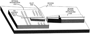
- FIG. 4A illustrates additional details about an optical interface between an optical waveguide on an OE-PCB 410 and an optical interposer 402 in accordance with the disclosed embodiments.
- FIG. 4A provides a top view of optical interposer 402 , which includes a light guide 406 , as well as a trapezoidal slot 408 , which is located on the bottom of interposer 402 .
- Board optical waveguide 404 which is located on OE-PCB 410 illustrated in FIG. 4B , has a compatible trapezoidal shape.
- FIG. 4B provides a perspective view of the same interface. This view illustrates how the board optical waveguide 404 , which has a trapezoidal shape, is located on an OE-PCB 410 .
- Optical interposer 402 has a corresponding trapezoidal slot, which is configured to accommodate the trapezoidal shape of board optical waveguide 404 to facilitate a relatively coarse alignment between board optical waveguide 404 and optical interposer 402 .
- FIG. 4B also illustrates C4 solder balls 412 , which are used to pull the optical interposer 402 into submicron alignment through solder reflow tension to provide a fine alignment for the optical connection between optical interposer 402 and OE-PCB 410 .
- FIG. 5 presents a flow chart illustrating a process for integrating an optical interposer with one or more electronic dies and an OE-PCB in accordance with the disclosed embodiments.
- This process involves first applying surface-connection elements to a surface of the optical interposer (step 502 ), and then bonding the one or more electrical dies to the optical interposer using the surface-connection elements (step 504 ).
- the method integrates the OE-PCB onto the surface of the optical interposer. This involves using triangular and/or trapezoidal shapes of mechanical alignment structures in the optical interposer and the OE-PCB to facilitate gross alignment during an initial pick-and-place assembly operation between the optical interposer and the OE-PCB (step 506 ).
- the process uses solder balls associated with the surface-connection elements to pull the optical interposer into submicron alignment through solder reflow tension to finely align an optical connection between the optical interposer and the OE-PCB (step 508 ).
Landscapes
- Physics & Mathematics (AREA)
- Engineering & Computer Science (AREA)
- General Physics & Mathematics (AREA)
- Microelectronics & Electronic Packaging (AREA)
- Power Engineering (AREA)
- Computer Hardware Design (AREA)
- Condensed Matter Physics & Semiconductors (AREA)
- Optics & Photonics (AREA)
- Manufacturing & Machinery (AREA)
- Ceramic Engineering (AREA)
- Optical Couplings Of Light Guides (AREA)
Abstract
Description
Claims (27)
Priority Applications (1)
| Application Number | Priority Date | Filing Date | Title |
|---|---|---|---|
| US16/375,667 US10859776B2 (en) | 2018-04-06 | 2019-04-04 | Optical-electrical interposers |
Applications Claiming Priority (2)
| Application Number | Priority Date | Filing Date | Title |
|---|---|---|---|
| US201862653802P | 2018-04-06 | 2018-04-06 | |
| US16/375,667 US10859776B2 (en) | 2018-04-06 | 2019-04-04 | Optical-electrical interposers |
Publications (2)
| Publication Number | Publication Date |
|---|---|
| US20190310433A1 US20190310433A1 (en) | 2019-10-10 |
| US10859776B2 true US10859776B2 (en) | 2020-12-08 |
Family
ID=68096476
Family Applications (1)
| Application Number | Title | Priority Date | Filing Date |
|---|---|---|---|
| US16/375,667 Active 2039-05-06 US10859776B2 (en) | 2018-04-06 | 2019-04-04 | Optical-electrical interposers |
Country Status (1)
| Country | Link |
|---|---|
| US (1) | US10859776B2 (en) |
Cited By (1)
| Publication number | Priority date | Publication date | Assignee | Title |
|---|---|---|---|---|
| US11156788B2 (en) * | 2016-07-14 | 2021-10-26 | Intel Corporation | Semiconductor package with embedded optical die |
Families Citing this family (4)
| Publication number | Priority date | Publication date | Assignee | Title |
|---|---|---|---|---|
| KR20220004966A (en) | 2019-03-06 | 2022-01-12 | 라이트매터, 인크. | photonic communication platform |
| US11443998B2 (en) * | 2019-06-05 | 2022-09-13 | Te Connectivity Solutions Gmbh | Electronic assembly including optical modules |
| KR20220137062A (en) * | 2020-02-03 | 2022-10-11 | 라이트매터, 인크. | Photonic Wafer Communication Systems and Related Packages |
| TW202217377A (en) | 2020-07-06 | 2022-05-01 | 新加坡商光子智能私人有限公司 | Integrated circuit interposer, system, apparatus, method of fabricating integrated circuit interposer, and method and system for transmitting information from nodes to destination interposer |
Citations (12)
| Publication number | Priority date | Publication date | Assignee | Title |
|---|---|---|---|---|
| US20030007750A1 (en) | 2000-03-28 | 2003-01-09 | Kryzak Charles J. | Passive self-alignment technique for array laser transmitters and receivers for fiber optic applications |
| US20080284037A1 (en) * | 2007-05-15 | 2008-11-20 | Andry Paul S | Apparatus and Methods for Constructing Semiconductor Chip Packages with Silicon Space Transformer Carriers |
| US20090267171A1 (en) * | 2008-04-24 | 2009-10-29 | Micron Technology, Inc. | Pre-encapsulated cavity interposer |
| US7999383B2 (en) * | 2006-07-21 | 2011-08-16 | Bae Systems Information And Electronic Systems Integration Inc. | High speed, high density, low power die interconnect system |
| US20130267273A1 (en) * | 2012-04-05 | 2013-10-10 | Heptagon Micro Optics Pte.Ltd. | Reflowable opto-electronic module |
| US20140029639A1 (en) * | 2011-12-28 | 2014-01-30 | Edward A. Zarbock | Photonic package architecture |
| US8709880B2 (en) * | 2010-07-30 | 2014-04-29 | Monolithic 3D Inc | Method for fabrication of a semiconductor device and structure |
| US20160071818A1 (en) * | 2014-09-05 | 2016-03-10 | Invensas Corporation | Multichip modules and methods of fabrication |
| US20170237516A1 (en) * | 2015-11-18 | 2017-08-17 | Luxtera, Inc. | Method and System for Cassette Based Wavelength Division Multiplexing |
| US20180267265A1 (en) * | 2017-02-06 | 2018-09-20 | Oracle International Corporation | Reflow-compatible optical i/o assembly adapter |
| US20180292607A1 (en) * | 2017-04-10 | 2018-10-11 | Alcatel-Lucent Usa Inc. | Modular optical device and modules therefor |
| US20190302379A1 (en) * | 2016-07-14 | 2019-10-03 | Intel Corporation | Semiconductor package with embedded optical die |
-
2019
- 2019-04-04 US US16/375,667 patent/US10859776B2/en active Active
Patent Citations (12)
| Publication number | Priority date | Publication date | Assignee | Title |
|---|---|---|---|---|
| US20030007750A1 (en) | 2000-03-28 | 2003-01-09 | Kryzak Charles J. | Passive self-alignment technique for array laser transmitters and receivers for fiber optic applications |
| US7999383B2 (en) * | 2006-07-21 | 2011-08-16 | Bae Systems Information And Electronic Systems Integration Inc. | High speed, high density, low power die interconnect system |
| US20080284037A1 (en) * | 2007-05-15 | 2008-11-20 | Andry Paul S | Apparatus and Methods for Constructing Semiconductor Chip Packages with Silicon Space Transformer Carriers |
| US20090267171A1 (en) * | 2008-04-24 | 2009-10-29 | Micron Technology, Inc. | Pre-encapsulated cavity interposer |
| US8709880B2 (en) * | 2010-07-30 | 2014-04-29 | Monolithic 3D Inc | Method for fabrication of a semiconductor device and structure |
| US20140029639A1 (en) * | 2011-12-28 | 2014-01-30 | Edward A. Zarbock | Photonic package architecture |
| US20130267273A1 (en) * | 2012-04-05 | 2013-10-10 | Heptagon Micro Optics Pte.Ltd. | Reflowable opto-electronic module |
| US20160071818A1 (en) * | 2014-09-05 | 2016-03-10 | Invensas Corporation | Multichip modules and methods of fabrication |
| US20170237516A1 (en) * | 2015-11-18 | 2017-08-17 | Luxtera, Inc. | Method and System for Cassette Based Wavelength Division Multiplexing |
| US20190302379A1 (en) * | 2016-07-14 | 2019-10-03 | Intel Corporation | Semiconductor package with embedded optical die |
| US20180267265A1 (en) * | 2017-02-06 | 2018-09-20 | Oracle International Corporation | Reflow-compatible optical i/o assembly adapter |
| US20180292607A1 (en) * | 2017-04-10 | 2018-10-11 | Alcatel-Lucent Usa Inc. | Modular optical device and modules therefor |
Cited By (3)
| Publication number | Priority date | Publication date | Assignee | Title |
|---|---|---|---|---|
| US11156788B2 (en) * | 2016-07-14 | 2021-10-26 | Intel Corporation | Semiconductor package with embedded optical die |
| US20210405306A1 (en) * | 2016-07-14 | 2021-12-30 | Intel Corporation | Semiconductor package with embedded optical die |
| US12078853B2 (en) * | 2016-07-14 | 2024-09-03 | Intel Corporation | Semiconductor package with embedded optical die |
Also Published As
| Publication number | Publication date |
|---|---|
| US20190310433A1 (en) | 2019-10-10 |
Similar Documents
| Publication | Publication Date | Title |
|---|---|---|
| US10859776B2 (en) | Optical-electrical interposers | |
| US9256026B2 (en) | Hybrid integrated photonic chip package | |
| US9297971B2 (en) | Hybrid-integrated photonic chip package with an interposer | |
| US9250403B2 (en) | Hybrid-integrated photonic chip package with an interposer | |
| US9678271B2 (en) | Packaged opto-electronic module | |
| US9671572B2 (en) | Integrated chip package with optical interface | |
| US9490240B2 (en) | Film interposer for integrated circuit devices | |
| US8998509B2 (en) | Stackable photonic interconnect module | |
| US20180180808A1 (en) | Wafer-level packaged optoelectronic module | |
| US11550106B2 (en) | Slim connector plug and active optical cable assembly using same | |
| CN110261974B (en) | Optical interconnection module and system comprising same | |
| US20060120666A1 (en) | Optical waveguide device, manufacturing method thereof, optical information processing apparatus, and electronic equipment | |
| US20090280601A1 (en) | Method and apparatus for facilitating proximity communication and power delivery | |
| TWI721112B (en) | Optoelectronic transceiver assemblies | |
| US10012792B2 (en) | Three-dimensional integrated photonic structure with improved optical properties | |
| US20240310578A1 (en) | Co-packaged optics assemblies | |
| CN218767433U (en) | Optical module | |
| CN209879081U (en) | Optical interconnection module and system comprising same | |
| CN113169234A (en) | High density optical interconnect assembly | |
| JP2006140295A (en) | Manufacturing method for semiconductor device | |
| US20230305244A1 (en) | High density optical/electrical interconnection arrangement with high thermal efficiency | |
| EP4421852A1 (en) | Photoelectric transceiver assembly and method for manufacturing same | |
| CN117849960A (en) | Optical module | |
| TWI447590B (en) | Usb optical card structure | |
| CN115185045A (en) | Optical fiber remote processor module structure |
Legal Events
| Date | Code | Title | Description |
|---|---|---|---|
| FEPP | Fee payment procedure |
Free format text: ENTITY STATUS SET TO UNDISCOUNTED (ORIGINAL EVENT CODE: BIG.); ENTITY STATUS OF PATENT OWNER: SMALL ENTITY |
|
| FEPP | Fee payment procedure |
Free format text: ENTITY STATUS SET TO SMALL (ORIGINAL EVENT CODE: SMAL); ENTITY STATUS OF PATENT OWNER: SMALL ENTITY |
|
| AS | Assignment |
Owner name: THE REGENTS OF THE UNIVERSITY OF CALIFORNIA, CALIF Free format text: ASSIGNMENT OF ASSIGNORS INTEREST;ASSIGNORS:YOO, SUNG-JOO BEN;PATTI, ROBERT S;SIGNING DATES FROM 20190405 TO 20190426;REEL/FRAME:049007/0479 Owner name: THE REGENTS OF THE UNIVERSITY OF CALIFORNIA, CALIFORNIA Free format text: ASSIGNMENT OF ASSIGNORS INTEREST;ASSIGNORS:YOO, SUNG-JOO BEN;PATTI, ROBERT S;SIGNING DATES FROM 20190405 TO 20190426;REEL/FRAME:049007/0479 |
|
| STPP | Information on status: patent application and granting procedure in general |
Free format text: NON FINAL ACTION MAILED |
|
| STPP | Information on status: patent application and granting procedure in general |
Free format text: PUBLICATIONS -- ISSUE FEE PAYMENT VERIFIED |
|
| STCF | Information on status: patent grant |
Free format text: PATENTED CASE |
|
| MAFP | Maintenance fee payment |
Free format text: PAYMENT OF MAINTENANCE FEE, 4TH YR, SMALL ENTITY (ORIGINAL EVENT CODE: M2551); ENTITY STATUS OF PATENT OWNER: SMALL ENTITY Year of fee payment: 4 |