EP2833397A1 - Substrat für leistungsmodul und herstellungsverfahren dafür - Google Patents
Substrat für leistungsmodul und herstellungsverfahren dafür Download PDFInfo
- Publication number
- EP2833397A1 EP2833397A1 EP13768726.5A EP13768726A EP2833397A1 EP 2833397 A1 EP2833397 A1 EP 2833397A1 EP 13768726 A EP13768726 A EP 13768726A EP 2833397 A1 EP2833397 A1 EP 2833397A1
- Authority
- EP
- European Patent Office
- Prior art keywords
- metal plate
- power
- ceramic substrate
- bonding
- less
- Prior art date
- Legal status (The legal status is an assumption and is not a legal conclusion. Google has not performed a legal analysis and makes no representation as to the accuracy of the status listed.)
- Granted
Links
Images

Classifications
-
- B—PERFORMING OPERATIONS; TRANSPORTING
- B23—MACHINE TOOLS; METAL-WORKING NOT OTHERWISE PROVIDED FOR
- B23K—SOLDERING OR UNSOLDERING; WELDING; CLADDING OR PLATING BY SOLDERING OR WELDING; CUTTING BY APPLYING HEAT LOCALLY, e.g. FLAME CUTTING; WORKING BY LASER BEAM
- B23K1/00—Soldering, e.g. brazing, or unsoldering
- B23K1/0008—Soldering, e.g. brazing, or unsoldering specially adapted for particular articles or work
- B23K1/0016—Soldering of electronic components
-
- B—PERFORMING OPERATIONS; TRANSPORTING
- B23—MACHINE TOOLS; METAL-WORKING NOT OTHERWISE PROVIDED FOR
- B23K—SOLDERING OR UNSOLDERING; WELDING; CLADDING OR PLATING BY SOLDERING OR WELDING; CUTTING BY APPLYING HEAT LOCALLY, e.g. FLAME CUTTING; WORKING BY LASER BEAM
- B23K1/00—Soldering, e.g. brazing, or unsoldering
- B23K1/19—Soldering, e.g. brazing, or unsoldering taking account of the properties of the materials to be soldered
-
- B—PERFORMING OPERATIONS; TRANSPORTING
- B32—LAYERED PRODUCTS
- B32B—LAYERED PRODUCTS, i.e. PRODUCTS BUILT-UP OF STRATA OF FLAT OR NON-FLAT, e.g. CELLULAR OR HONEYCOMB, FORM
- B32B15/00—Layered products comprising a layer of metal
- B32B15/04—Layered products comprising a layer of metal comprising metal as the main or only constituent of a layer, which is next to another layer of the same or of a different material
-
- B—PERFORMING OPERATIONS; TRANSPORTING
- B32—LAYERED PRODUCTS
- B32B—LAYERED PRODUCTS, i.e. PRODUCTS BUILT-UP OF STRATA OF FLAT OR NON-FLAT, e.g. CELLULAR OR HONEYCOMB, FORM
- B32B18/00—Layered products essentially comprising ceramics, e.g. refractory products
-
- C—CHEMISTRY; METALLURGY
- C04—CEMENTS; CONCRETE; ARTIFICIAL STONE; CERAMICS; REFRACTORIES
- C04B—LIME, MAGNESIA; SLAG; CEMENTS; COMPOSITIONS THEREOF, e.g. MORTARS, CONCRETE OR LIKE BUILDING MATERIALS; ARTIFICIAL STONE; CERAMICS; REFRACTORIES; TREATMENT OF NATURAL STONE
- C04B37/00—Joining burned ceramic articles with other burned ceramic articles or other articles by heating
- C04B37/02—Joining burned ceramic articles with other burned ceramic articles or other articles by heating with metallic articles
- C04B37/023—Joining burned ceramic articles with other burned ceramic articles or other articles by heating with metallic articles characterised by the interlayer used
- C04B37/026—Joining burned ceramic articles with other burned ceramic articles or other articles by heating with metallic articles characterised by the interlayer used consisting of metals or metal salts
-
- H—ELECTRICITY
- H05—ELECTRIC TECHNIQUES NOT OTHERWISE PROVIDED FOR
- H05K—PRINTED CIRCUITS; CASINGS OR CONSTRUCTIONAL DETAILS OF ELECTRIC APPARATUS; MANUFACTURE OF ASSEMBLAGES OF ELECTRICAL COMPONENTS
- H05K3/00—Apparatus or processes for manufacturing printed circuits
- H05K3/38—Improvement of the adhesion between the insulating substrate and the metal
- H05K3/382—Improvement of the adhesion between the insulating substrate and the metal by special treatment of the metal
- H05K3/383—Improvement of the adhesion between the insulating substrate and the metal by special treatment of the metal by microetching
-
- H—ELECTRICITY
- H10—SEMICONDUCTOR DEVICES; ELECTRIC SOLID-STATE DEVICES NOT OTHERWISE PROVIDED FOR
- H10W—GENERIC PACKAGES, INTERCONNECTIONS, CONNECTORS OR OTHER CONSTRUCTIONAL DETAILS OF DEVICES COVERED BY CLASS H10
- H10W40/00—Arrangements for thermal protection or thermal control
- H10W40/20—Arrangements for cooling
- H10W40/25—Arrangements for cooling characterised by their materials
- H10W40/255—Arrangements for cooling characterised by their materials having a laminate or multilayered structure, e.g. direct bond copper [DBC] ceramic substrates
-
- B—PERFORMING OPERATIONS; TRANSPORTING
- B32—LAYERED PRODUCTS
- B32B—LAYERED PRODUCTS, i.e. PRODUCTS BUILT-UP OF STRATA OF FLAT OR NON-FLAT, e.g. CELLULAR OR HONEYCOMB, FORM
- B32B2457/00—Electrical equipment
-
- C—CHEMISTRY; METALLURGY
- C04—CEMENTS; CONCRETE; ARTIFICIAL STONE; CERAMICS; REFRACTORIES
- C04B—LIME, MAGNESIA; SLAG; CEMENTS; COMPOSITIONS THEREOF, e.g. MORTARS, CONCRETE OR LIKE BUILDING MATERIALS; ARTIFICIAL STONE; CERAMICS; REFRACTORIES; TREATMENT OF NATURAL STONE
- C04B2235/00—Aspects relating to ceramic starting mixtures or sintered ceramic products
- C04B2235/65—Aspects relating to heat treatments of ceramic bodies such as green ceramics or pre-sintered ceramics, e.g. burning, sintering or melting processes
- C04B2235/658—Atmosphere during thermal treatment
- C04B2235/6581—Total pressure below 1 atmosphere, e.g. vacuum
-
- C—CHEMISTRY; METALLURGY
- C04—CEMENTS; CONCRETE; ARTIFICIAL STONE; CERAMICS; REFRACTORIES
- C04B—LIME, MAGNESIA; SLAG; CEMENTS; COMPOSITIONS THEREOF, e.g. MORTARS, CONCRETE OR LIKE BUILDING MATERIALS; ARTIFICIAL STONE; CERAMICS; REFRACTORIES; TREATMENT OF NATURAL STONE
- C04B2235/00—Aspects relating to ceramic starting mixtures or sintered ceramic products
- C04B2235/70—Aspects relating to sintered or melt-casted ceramic products
- C04B2235/72—Products characterised by the absence or the low content of specific components, e.g. alkali metal free alumina ceramics
- C04B2235/723—Oxygen content
-
- C—CHEMISTRY; METALLURGY
- C04—CEMENTS; CONCRETE; ARTIFICIAL STONE; CERAMICS; REFRACTORIES
- C04B—LIME, MAGNESIA; SLAG; CEMENTS; COMPOSITIONS THEREOF, e.g. MORTARS, CONCRETE OR LIKE BUILDING MATERIALS; ARTIFICIAL STONE; CERAMICS; REFRACTORIES; TREATMENT OF NATURAL STONE
- C04B2235/00—Aspects relating to ceramic starting mixtures or sintered ceramic products
- C04B2235/70—Aspects relating to sintered or melt-casted ceramic products
- C04B2235/96—Properties of ceramic products, e.g. mechanical properties such as strength, toughness, wear resistance
- C04B2235/963—Surface properties, e.g. surface roughness
-
- C—CHEMISTRY; METALLURGY
- C04—CEMENTS; CONCRETE; ARTIFICIAL STONE; CERAMICS; REFRACTORIES
- C04B—LIME, MAGNESIA; SLAG; CEMENTS; COMPOSITIONS THEREOF, e.g. MORTARS, CONCRETE OR LIKE BUILDING MATERIALS; ARTIFICIAL STONE; CERAMICS; REFRACTORIES; TREATMENT OF NATURAL STONE
- C04B2237/00—Aspects relating to ceramic laminates or to joining of ceramic articles with other articles by heating
- C04B2237/02—Aspects relating to interlayers, e.g. used to join ceramic articles with other articles by heating
- C04B2237/04—Ceramic interlayers
- C04B2237/06—Oxidic interlayers
- C04B2237/064—Oxidic interlayers based on alumina or aluminates
-
- C—CHEMISTRY; METALLURGY
- C04—CEMENTS; CONCRETE; ARTIFICIAL STONE; CERAMICS; REFRACTORIES
- C04B—LIME, MAGNESIA; SLAG; CEMENTS; COMPOSITIONS THEREOF, e.g. MORTARS, CONCRETE OR LIKE BUILDING MATERIALS; ARTIFICIAL STONE; CERAMICS; REFRACTORIES; TREATMENT OF NATURAL STONE
- C04B2237/00—Aspects relating to ceramic laminates or to joining of ceramic articles with other articles by heating
- C04B2237/02—Aspects relating to interlayers, e.g. used to join ceramic articles with other articles by heating
- C04B2237/12—Metallic interlayers
- C04B2237/121—Metallic interlayers based on aluminium
-
- C—CHEMISTRY; METALLURGY
- C04—CEMENTS; CONCRETE; ARTIFICIAL STONE; CERAMICS; REFRACTORIES
- C04B—LIME, MAGNESIA; SLAG; CEMENTS; COMPOSITIONS THEREOF, e.g. MORTARS, CONCRETE OR LIKE BUILDING MATERIALS; ARTIFICIAL STONE; CERAMICS; REFRACTORIES; TREATMENT OF NATURAL STONE
- C04B2237/00—Aspects relating to ceramic laminates or to joining of ceramic articles with other articles by heating
- C04B2237/02—Aspects relating to interlayers, e.g. used to join ceramic articles with other articles by heating
- C04B2237/12—Metallic interlayers
- C04B2237/126—Metallic interlayers wherein the active component for bonding is not the largest fraction of the interlayer
- C04B2237/128—The active component for bonding being silicon
-
- C—CHEMISTRY; METALLURGY
- C04—CEMENTS; CONCRETE; ARTIFICIAL STONE; CERAMICS; REFRACTORIES
- C04B—LIME, MAGNESIA; SLAG; CEMENTS; COMPOSITIONS THEREOF, e.g. MORTARS, CONCRETE OR LIKE BUILDING MATERIALS; ARTIFICIAL STONE; CERAMICS; REFRACTORIES; TREATMENT OF NATURAL STONE
- C04B2237/00—Aspects relating to ceramic laminates or to joining of ceramic articles with other articles by heating
- C04B2237/30—Composition of layers of ceramic laminates or of ceramic or metallic articles to be joined by heating, e.g. Si substrates
- C04B2237/32—Ceramic
- C04B2237/36—Non-oxidic
- C04B2237/366—Aluminium nitride
-
- C—CHEMISTRY; METALLURGY
- C04—CEMENTS; CONCRETE; ARTIFICIAL STONE; CERAMICS; REFRACTORIES
- C04B—LIME, MAGNESIA; SLAG; CEMENTS; COMPOSITIONS THEREOF, e.g. MORTARS, CONCRETE OR LIKE BUILDING MATERIALS; ARTIFICIAL STONE; CERAMICS; REFRACTORIES; TREATMENT OF NATURAL STONE
- C04B2237/00—Aspects relating to ceramic laminates or to joining of ceramic articles with other articles by heating
- C04B2237/30—Composition of layers of ceramic laminates or of ceramic or metallic articles to be joined by heating, e.g. Si substrates
- C04B2237/40—Metallic
- C04B2237/402—Aluminium
-
- C—CHEMISTRY; METALLURGY
- C04—CEMENTS; CONCRETE; ARTIFICIAL STONE; CERAMICS; REFRACTORIES
- C04B—LIME, MAGNESIA; SLAG; CEMENTS; COMPOSITIONS THEREOF, e.g. MORTARS, CONCRETE OR LIKE BUILDING MATERIALS; ARTIFICIAL STONE; CERAMICS; REFRACTORIES; TREATMENT OF NATURAL STONE
- C04B2237/00—Aspects relating to ceramic laminates or to joining of ceramic articles with other articles by heating
- C04B2237/50—Processing aspects relating to ceramic laminates or to the joining of ceramic articles with other articles by heating
- C04B2237/52—Pre-treatment of the joining surfaces, e.g. cleaning, machining
-
- C—CHEMISTRY; METALLURGY
- C04—CEMENTS; CONCRETE; ARTIFICIAL STONE; CERAMICS; REFRACTORIES
- C04B—LIME, MAGNESIA; SLAG; CEMENTS; COMPOSITIONS THEREOF, e.g. MORTARS, CONCRETE OR LIKE BUILDING MATERIALS; ARTIFICIAL STONE; CERAMICS; REFRACTORIES; TREATMENT OF NATURAL STONE
- C04B2237/00—Aspects relating to ceramic laminates or to joining of ceramic articles with other articles by heating
- C04B2237/50—Processing aspects relating to ceramic laminates or to the joining of ceramic articles with other articles by heating
- C04B2237/59—Aspects relating to the structure of the interlayer
- C04B2237/592—Aspects relating to the structure of the interlayer whereby the interlayer is not continuous, e.g. not the whole surface of the smallest substrate is covered by the interlayer
-
- C—CHEMISTRY; METALLURGY
- C04—CEMENTS; CONCRETE; ARTIFICIAL STONE; CERAMICS; REFRACTORIES
- C04B—LIME, MAGNESIA; SLAG; CEMENTS; COMPOSITIONS THEREOF, e.g. MORTARS, CONCRETE OR LIKE BUILDING MATERIALS; ARTIFICIAL STONE; CERAMICS; REFRACTORIES; TREATMENT OF NATURAL STONE
- C04B2237/00—Aspects relating to ceramic laminates or to joining of ceramic articles with other articles by heating
- C04B2237/50—Processing aspects relating to ceramic laminates or to the joining of ceramic articles with other articles by heating
- C04B2237/60—Forming at the joining interface or in the joining layer specific reaction phases or zones, e.g. diffusion of reactive species from the interlayer to the substrate or from a substrate to the joining interface, carbide forming at the joining interface
-
- C—CHEMISTRY; METALLURGY
- C04—CEMENTS; CONCRETE; ARTIFICIAL STONE; CERAMICS; REFRACTORIES
- C04B—LIME, MAGNESIA; SLAG; CEMENTS; COMPOSITIONS THEREOF, e.g. MORTARS, CONCRETE OR LIKE BUILDING MATERIALS; ARTIFICIAL STONE; CERAMICS; REFRACTORIES; TREATMENT OF NATURAL STONE
- C04B2237/00—Aspects relating to ceramic laminates or to joining of ceramic articles with other articles by heating
- C04B2237/50—Processing aspects relating to ceramic laminates or to the joining of ceramic articles with other articles by heating
- C04B2237/70—Forming laminates or joined articles comprising layers of a specific, unusual thickness
- C04B2237/704—Forming laminates or joined articles comprising layers of a specific, unusual thickness of one or more of the ceramic layers or articles
-
- C—CHEMISTRY; METALLURGY
- C04—CEMENTS; CONCRETE; ARTIFICIAL STONE; CERAMICS; REFRACTORIES
- C04B—LIME, MAGNESIA; SLAG; CEMENTS; COMPOSITIONS THEREOF, e.g. MORTARS, CONCRETE OR LIKE BUILDING MATERIALS; ARTIFICIAL STONE; CERAMICS; REFRACTORIES; TREATMENT OF NATURAL STONE
- C04B2237/00—Aspects relating to ceramic laminates or to joining of ceramic articles with other articles by heating
- C04B2237/50—Processing aspects relating to ceramic laminates or to the joining of ceramic articles with other articles by heating
- C04B2237/70—Forming laminates or joined articles comprising layers of a specific, unusual thickness
- C04B2237/706—Forming laminates or joined articles comprising layers of a specific, unusual thickness of one or more of the metallic layers or articles
-
- C—CHEMISTRY; METALLURGY
- C04—CEMENTS; CONCRETE; ARTIFICIAL STONE; CERAMICS; REFRACTORIES
- C04B—LIME, MAGNESIA; SLAG; CEMENTS; COMPOSITIONS THEREOF, e.g. MORTARS, CONCRETE OR LIKE BUILDING MATERIALS; ARTIFICIAL STONE; CERAMICS; REFRACTORIES; TREATMENT OF NATURAL STONE
- C04B2237/00—Aspects relating to ceramic laminates or to joining of ceramic articles with other articles by heating
- C04B2237/50—Processing aspects relating to ceramic laminates or to the joining of ceramic articles with other articles by heating
- C04B2237/70—Forming laminates or joined articles comprising layers of a specific, unusual thickness
- C04B2237/708—Forming laminates or joined articles comprising layers of a specific, unusual thickness of one or more of the interlayers
-
- C—CHEMISTRY; METALLURGY
- C04—CEMENTS; CONCRETE; ARTIFICIAL STONE; CERAMICS; REFRACTORIES
- C04B—LIME, MAGNESIA; SLAG; CEMENTS; COMPOSITIONS THEREOF, e.g. MORTARS, CONCRETE OR LIKE BUILDING MATERIALS; ARTIFICIAL STONE; CERAMICS; REFRACTORIES; TREATMENT OF NATURAL STONE
- C04B2237/00—Aspects relating to ceramic laminates or to joining of ceramic articles with other articles by heating
- C04B2237/50—Processing aspects relating to ceramic laminates or to the joining of ceramic articles with other articles by heating
- C04B2237/72—Forming laminates or joined articles comprising at least two interlayers directly next to each other
-
- C—CHEMISTRY; METALLURGY
- C04—CEMENTS; CONCRETE; ARTIFICIAL STONE; CERAMICS; REFRACTORIES
- C04B—LIME, MAGNESIA; SLAG; CEMENTS; COMPOSITIONS THEREOF, e.g. MORTARS, CONCRETE OR LIKE BUILDING MATERIALS; ARTIFICIAL STONE; CERAMICS; REFRACTORIES; TREATMENT OF NATURAL STONE
- C04B2237/00—Aspects relating to ceramic laminates or to joining of ceramic articles with other articles by heating
- C04B2237/50—Processing aspects relating to ceramic laminates or to the joining of ceramic articles with other articles by heating
- C04B2237/86—Joining of two substrates at their largest surfaces, one surface being complete joined and covered, the other surface not, e.g. a small plate joined at it's largest surface on top of a larger plate
-
- H—ELECTRICITY
- H05—ELECTRIC TECHNIQUES NOT OTHERWISE PROVIDED FOR
- H05K—PRINTED CIRCUITS; CASINGS OR CONSTRUCTIONAL DETAILS OF ELECTRIC APPARATUS; MANUFACTURE OF ASSEMBLAGES OF ELECTRICAL COMPONENTS
- H05K1/00—Printed circuits
- H05K1/02—Details
- H05K1/03—Use of materials for the substrate
- H05K1/0306—Inorganic insulating substrates, e.g. ceramic, glass
-
- H—ELECTRICITY
- H05—ELECTRIC TECHNIQUES NOT OTHERWISE PROVIDED FOR
- H05K—PRINTED CIRCUITS; CASINGS OR CONSTRUCTIONAL DETAILS OF ELECTRIC APPARATUS; MANUFACTURE OF ASSEMBLAGES OF ELECTRICAL COMPONENTS
- H05K3/00—Apparatus or processes for manufacturing printed circuits
- H05K3/38—Improvement of the adhesion between the insulating substrate and the metal
- H05K3/382—Improvement of the adhesion between the insulating substrate and the metal by special treatment of the metal
-
- H—ELECTRICITY
- H10—SEMICONDUCTOR DEVICES; ELECTRIC SOLID-STATE DEVICES NOT OTHERWISE PROVIDED FOR
- H10W—GENERIC PACKAGES, INTERCONNECTIONS, CONNECTORS OR OTHER CONSTRUCTIONAL DETAILS OF DEVICES COVERED BY CLASS H10
- H10W40/00—Arrangements for thermal protection or thermal control
- H10W40/20—Arrangements for cooling
- H10W40/25—Arrangements for cooling characterised by their materials
- H10W40/258—Metallic materials
-
- H—ELECTRICITY
- H10—SEMICONDUCTOR DEVICES; ELECTRIC SOLID-STATE DEVICES NOT OTHERWISE PROVIDED FOR
- H10W—GENERIC PACKAGES, INTERCONNECTIONS, CONNECTORS OR OTHER CONSTRUCTIONAL DETAILS OF DEVICES COVERED BY CLASS H10
- H10W40/00—Arrangements for thermal protection or thermal control
- H10W40/40—Arrangements for thermal protection or thermal control involving heat exchange by flowing fluids
- H10W40/47—Arrangements for thermal protection or thermal control involving heat exchange by flowing fluids by flowing liquids, e.g. forced water cooling
-
- H—ELECTRICITY
- H10—SEMICONDUCTOR DEVICES; ELECTRIC SOLID-STATE DEVICES NOT OTHERWISE PROVIDED FOR
- H10W—GENERIC PACKAGES, INTERCONNECTIONS, CONNECTORS OR OTHER CONSTRUCTIONAL DETAILS OF DEVICES COVERED BY CLASS H10
- H10W72/00—Interconnections or connectors in packages
- H10W72/851—Dispositions of multiple connectors or interconnections
- H10W72/874—On different surfaces
- H10W72/884—Die-attach connectors and bond wires
Definitions
- the present invention relates to a power-module substrate configuring a power module controlling a large electric current and a large voltage and a manufacturing method thereof.
- a power module having a structure in which electronic components such as a semiconductor chip and the like are mounted on a power-module substrate is known.
- a manufacturing method of the power module for example, methods described in Patent Document 1 and Patent Document 2 are known. In these methods: a metal plate being a circuit layer is stacked on one surface of a ceramic substrate interposing brazing material; a metal plate being a heat-radiation layer is stacked on the other surface of the ceramic substrate interposing the brazing material; and those are pressed in a stacking direction and heated so as to bond the metal plates to the ceramic substrate, so that a power-module substrate is manufactured.
- a top plate part of a heat sink is stacked on a surface of the heat-radiation layer that is opposite to the surface to which the ceramic substrate is bonded interposing the brazing material; and the heat-radiation layer and the heat sink are pressed in this stacking direction and heated so as to bond to each other, so that a power-module substrate with a heat sink is manufactured.
- Patent Document 3 as a bonding method of a top plate of a heat sink and a metal plate of a power-module substrate, it is described to braze with spreading flux.
- This brazing is a method of bonding by removing oxide on a brazing face by spreading fluoride-based flux on the brazing face and heating in non-oxidizing atmosphere, in which expensive equipment is not necessary and it is comparatively easy to braze stably.
- the present invention is achieved in consideration of the above circumstances, and has an object to provide a power-module substrate and a manufacturing method thereof in which small voids are reduced at a bonded part and separation can be prevented.
- a power-module substrate according to the present invention is made by bonding a metal plate made of aluminum or aluminum alloy to at least one surface of a ceramic substrate by brazing, in which: when a cross section of the metal plate is observed by a scanning electron microscope in a field of 3000 magnifications in a depth extent of 5 ⁇ m from a bonded interface between the metal plate and the ceramic substrate in a width area of 200 ⁇ m from a side edge of the metal plate, residual-continuous oxides existing continuously by 2 ⁇ m or more along the bonded interface has total length of 70% or less with respect to a length of the field.
- the residual-continuous oxides are that have a length of 2 ⁇ m or more out of residual oxide existing along the bonded interface. If a plurality of the residual oxides having the length of 2 ⁇ m or more exist in an observation field, the total length of them is 70% or less of a length of the observation field. Adjacent residual oxides are regarded to be continuous when a distance between the adjacent residual oxides is 1 ⁇ m or less, even if a length thereof is less than 2 ⁇ m.
- a manufacturing method of power-module substrate according to the present invention is a method of manufacturing the power-module substrate by bonding a metal plate made of aluminum or aluminum alloy to at least one surface of a ceramic substrate by brazing, using the metal plate having an oxygen concentration of 1.5 mass% or less analyzed from a count number of oxygen measured by an electron probe micro analyzer by an accelerating voltage 10 kV, an electric current 100 mA, and a beam diameter 100 ⁇ m, and an oxide thickness of 35 ⁇ or less measured by an X-ray photoelectron spectroscopy analysis in a thickness direction as the metal plate before bonding to the ceramic substrate.
- the metal plate having the oxygen concentration and the oxide thickness in the above measured values as the previous state of bonding to the ceramic substrate, it is possible to reduce residual-continuous oxides after bonding and prevent the small voids from being generated.
- 1.3 ⁇ m or more of a surface layer of the metal plate may be removed before bonding the metal plate to the ceramic substrate.
- an oxide film generated on a surface of the metal plate is generally supposed. However, if removing merely the oxide film, the residual oxide at the bonded part is not disappeared.
- the inventors found that wear debris and the like when the metal plate was rolled was buried in the surface of the metal plate, and oxide of the wear debris and the like were remained in the bonded part. Since the wear debris and the like are rough and large with comparing to the oxide film on the surface of the metal plate, it is necessary to remove the surface layer 1.3 ⁇ m or more in order to remove the wear debris and the like. Etching is suitable to remove it; and blasting, or combination of blasting and etching may be applied.
- arithmetic-mean-roughness Ra of a surface of the metal plate be 0.05 ⁇ m or more and 0.30 ⁇ m or less before bonding to the ceramic substrate.
- the oxide is divided by fine roughness generated on the surface of the metal plate, and the brazing material melted while brazing is divided and flows isotropically in the bonded surface. As a result, the oxide is restrained from being converged to a specific end part, and it is possible to reduce the residual-continuous oxides existing continuously by 2 ⁇ m or more.
- a difference between arithmetic-mean-roughness along a rolling direction of the metal plate and arithmetic-mean-roughness along a perpendicular direction to the rolling direction be 0.1 ⁇ m or less.
- the power-module substrate and the manufacturing method thereof of the present invention reducing the small voids in the bonded part between the ceramic substrate and the metal plate, the separation of the metal plate at the end part can be prevented, so that bonding reliability can be improved.
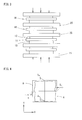
- FIG. 1 shows a power module 100 using a power-module substrate 10 according to the present invention.
- the power module 100 is configured from: the power-module substrate 10; an electronic component 20 such as a semiconductor chip or the like mounted on a surface of the power-module substrate 10; and a heat sink 30 bonded to the power-module substrate 10 on an opposite surface to the electronic component 20.
- the power-module substrate 10 is provided with a ceramic substrate 11, and metal plates 12 and 13 laminated on both surfaces of the ceramic substrate 11.
- the metal plate 12 laminated on one surface of the ceramic substrate 11 is to be a circuit layer in which the electronic component 20 is soldered on a surface thereof.
- the other metal plate 13 is to be a heat-radiation layer in which the heat sink 30 is mounted on a surface thereof.
- the ceramic substrate 11 is made ofAIN (aluminum nitride), and has a thickness of 635 ⁇ m, for example.
- the metal plates 12 and 13 are aluminum of purity 99 mass% or more: 1000s aluminum, especially, 1N90 (purity 99.9 mass% or more: i.e., 3N aluminum) or 1N99 (purity 99.99 mass% or more: i.e., 4N aluminum) by JIS standard can be applied. Also, aluminum alloys such as JIS A3003 and A6063 and the like can be applied.
- the metal plates 12 and 13 are formed as a rectangle-flat plate shape 30 mm each side, for example.
- the metal plate 13 being the heat-radiation layer is formed thicker than the metal plate 12 being the circuit layer in order to impart a function of absorbing a difference by thermal expansion between the ceramic substrate 11 and the heat sink 30 under a heat cycle.
- a thickness of the metal plate 12 is 600 ⁇ m; and a thickness of the metal plate 13 is 1600 ⁇ m.
- the metal plates 12 and 13 are bonded to the ceramic substrate 11 by brazing.
- brazing material alloys such as Al-Si-based, Al-Ge-based, Al-Cu-based, Al-Mg-based or Al-Mn-based or the like can be used.
- the residual-continuous oxide is that has a length of 2 ⁇ m or more out of residual oxide existing along the bonded interface. If a plurality of the residual oxides having the length of 2 ⁇ m or more exist in an observation field, the total length of them is 70% or less of a length of the observation field. Adjacent residual oxides are regarded to be continuous when a distance between the adjacent residual oxides is 1 ⁇ m or less, even if a length of the residual oxide is less than 2 ⁇ m.
- residual-continuous oxide Q is continuous for 2 ⁇ m or more; and single residual oxide R is adjacent with a mutual interval of 1 ⁇ m or more.
- a sum of lengths of the residual-continuous oxides Q is a length of the residual-continuous oxide (LI + L2 + L3). If a length of the observation field by SEM is L, the residual-continuous oxide exists by a rate (a percentage) of (LI + L2 + L3)/L with respect to the length of the observation field.
- the heat sink 30 is not limited to a specific shape, is formed from a material having an excellent thermal conductivity, e.g., aluminum alloy of A3000s, and has a plurality of passages 30a formed therein to let coolant (e.g., cooling water) flows therethrough.
- coolant e.g., cooling water
- the heat sink 30 and the metal plate 13 to be the heat-radiation layer of the power-module substrate 10 are bonded to each other by brazing.
- the brazing material alloys such as Al-Si-based, Al-Ge-based, Al-Cu-based, Al-Mg-based or Al-Mn-based or the like can be used.
- a plating layer 21 of NiP or the like is formed on a surface of the metal plate 12 to be the circuit layer; and the electronic component 20 is bonded on the plating layer.
- soldering material such as Sn-Ag-Cu-based, Sn-Cu-based, Sn-Ag-based, Sn-Sb-based, Zn-Al-based or Pb-Sn-based or the like is used.
- the reference symbol 22 indicates the solder-bonding layer in FIG. 1 .
- the electronic component 20 and terminal parts of the metal plate 12 are connected by bonding wires 23 made from aluminum.
- the power-module substrate 10 is formed by bonding the metal plates 12 and 13 to the ceramic substrate 11; and after that, the heat sink 30 is bonded to the metal plate 13.
- the metal plates 12 and 13 are formed by pressing sheet material.
- the metal plate 12 to be the circuit layer is formed by merely being stamped out from the sheet material.
- the metal plate 13 to be the heat-radiation layer is stamped out from the sheet material and processed.
- the etching process is carried out so that the metal plates 12 and 13 are soaked in an NaOH solution with a concentration of 5% as etchant with solution temperature of 50°C for a prescribed time.
- Process time is set so that 1.3 ⁇ m or more of surface layers of the metal plates 12 and 13 can be removed.
- An etching depth is obtained from a relation between specific gravities and areas of the metal plates 12 and 13 by calculating an etching amount from differences between a weight before processing and a weight after processing of the metal plates 12 and 13.
- the surfaces of the metal plates 12 and 13 have: oxygen concentrations of 1.5 mass% or less analyzed from a count number of oxygen measured by an electron probe micro analyzer (EPMA) by an accelerating voltage 10 kV, an electric current 100 mA, and a beam diameter 100 ⁇ m; and oxide thicknesses of 35 ⁇ or less measured by an X-ray photoelectron spectroscopy (XPS) analysis in a thickness direction.
- EPMA electron probe micro analyzer
- XPS X-ray photoelectron spectroscopy
- Measuring conditions of the X-ray photoelectron spectroscopy is set as: output power of an X-ray source is 100 W; pass energy is 26 eV; measuring step is 0.05 eV; a beam diameter is 100 ⁇ m ⁇ 1.4 mm as an analysis region; a detecting angle is 90°; and a detecting depth is 80 ⁇ .
- the oxide thickness is obtained by: separating waves of an oxide peak derived from the oxide and a metal peak of base metal from a spectrum obtained by the X-ray photoelectron spectroscopy; and assigning an area rate of the metal peak to a next Formula (1) by these data analysis.
- d 2.68 ⁇ ln 1 / A ⁇ 10
- the surfaces of the metal plates 12 and 13 after the etching process are formed to be rough with arithmetic-mean-roughness Ra of 0.05 ⁇ m or more and 0.30 ⁇ m or less.
- the metal plates 12 and 13 are made by rolling, a difference between the arithmetic-mean-roughness along a rolling direction and the arithmetic-mean-roughness along a perpendicular direction to the rolling direction is 0.10 ⁇ m or less, so that rolling lines and the like generated by rolling are removed and there is no directionality of surface roughness.
- the ceramic substrate 11 is stacked on a substrate-bonding surface 13b of the metal plate 13 with interposing the brazing material; and the other metal plate 12 is stacked on this ceramic substrate 11 with interposing the brazing material.
- a brazing-material foil be laminated in advance on sheet material when the metal plates 12 and 13 are stamped out from the sheet material by the pressing process so that the metal plates 12 and 13 on which the brazing-material foil is laminated are formed by stamping the sheet material together with the brazing-material foil.
- the ceramic substrate 11 and the metal plates 12 and 13 which are stacked on each other are brazed by being heated in vacuum atmosphere with being pressed in the thickness direction.
- a plurality of units of the ceramic substrates 11 and the metal plates 12 and 13 are stacked; cushion layers 25 made of carbon plates, graphite plates and the like are interposed between the units respectively; and these are pressed and heated in the stacked state.
- applied pressure is 0.1 to 2.5 MPa
- heating temperature is 630 to 655°C
- heating time is 1 to 60 minutes.
- the brazing material between the ceramic substrate 11 and the metal plates 12 and 13 is melted and fix them. Accordingly, the substrate-bonding surface 13b of the metal plate 13 and the ceramic substrate 11 are brazed, so that the power-module substrate 10 is manufactured.
- the brazing material between the ceramic substrate 11 and the metal plates 12 and 13 is melted into flow condition, the melted brazing material is not converged in one place but flows isotropically with being dispersed since the surface roughness of the metal plates 12 and 13 is 0.05 ⁇ m or more and 0.30 ⁇ m or less in Ra and the difference between the arithmetic-mean-roughness along the rolling direction and the arithmetic-mean-roughness perpendicular to the rolling direction is 0.10 ⁇ m or less.
- the brazing material flows along the rolling lines; if oxide is remained on the surface of the metal plate with such a surface state, the oxide flows together with the brazing material and is converged at end parts of the rolling lines.
- the metal plates 12 and 13 of the present embodiment are used, the oxides on the surfaces of the metal plates 12 and 13 are reduced; and even if the oxide is slightly remained, the brazing material is dispersed and flows isotropically, so that the oxide is not converged at a specific end part.
- the small voids are attached to the oxide, the small voids are not converged at a specific part of the bonded part and are dispersed.
- the cross section of the metal plates 12 and 13 are observed by the scanning electron microscope (SEM) in the field of 3000 magnifications in the depth extent of 5 ⁇ m from the bonded interface between the metal plates 12 and 13 and the ceramic substrate 11 in a width area of 200 ⁇ m from the side edges of the metal plates 12 and 13, the residual-continuous oxides existing continuously by 2 ⁇ m or more along the bonded interface has total length of 70% or less with respect to the length of the field.
- the plating layer 21 of Ni-P or the like is formed on the surface of the metal plate 12 to be the circuit layer, so that the power-module substrate 10 is obtained.
- the metal plate 13 to be the heat-radiation layer of the power-module substrate 10 and the heat sink 30 are bonded by a brazing method using flux (a Nocolok brazing method) so that the power-module substrate 10 and the heat sink 30 are bonded.
- a brazing method of brazing by applying fluoride-based flux on a surface of the brazing-material for removing oxide on a metal surface and heating at 600 to 615°C in a non-oxidation atmosphere (e.g., N 2 atmosphere).
- the brazing material for bonding the metal plate 13 and the heat sink 30 is, for example, Ai-Si-based alloy which is supplied by cladding on a surface of the heat sink 30 in advance or stacking on the heat sink 30 in a state of a brazing-material foil.
- the power-module substrate 10 is heated to 600°C or higher, if a large void is generated in the bonded part between the ceramic substrate 11 and the metal plates 12 and 13, the flux enters from the void and causes the separation. In the power-module substrate 10 of the present embodiment, since the voids are small and dispersed even if generated as described above, the separation is not occurred.
- This flux is for cleaning the metal surface in brazing by washing away the oxide. In order to prevent the flux from entering, it is enough if oxide that is easy to react with the flux does not exist.
- this power-module substrate 10 there are only the few residual-continuous oxides in a prescribed-width area from a side edge of the bonded part between the ceramic substrate 11 and the metal plate 13 to be the heat-radiation layer as described above; accordingly, the flux does not enter from this end part, so that the separation can be prevented from occurring.
- Rolled material of 1N99 aluminum having a thickness of 0.6 mm was stamped out into 30 mm ⁇ 30 mm; an etching process or a blast process shown in Table 1 was carried out; and a removed depth of a surface of a metal plate by the process was measured.
- the removed depth was obtained from a relation between specific gravity and area of the metal plate by calculating a removed amount from a difference between a weight before processing and a weight after processing of the metal plate.
- oxygen concentration was analyzed from a count number of oxygen by an electron probe micro analyzer (EPMA) by an accelerating voltage 10 kV, an electric current 100 mA, and a beam diameter 100 ⁇ m; and an oxide thickness was measured by an X-ray photoelectron spectroscopy (XPS) analysis in a thickness direction.
- EPMA electron probe micro analyzer
- XPS X-ray photoelectron spectroscopy
- Measuring conditions of X-ray photoelectron spectroscopy is set as: output power of an X-ray source is 100 W; pass energy is 26 eV; measuring step is 0.05 eV; a beam diameter is 100 ⁇ m ⁇ 1.4 mm as an analysis region; a detecting angle is 90°; and a detecting depth is 80 ⁇ .
- a thickness was obtained from the above-mentioned Formula (1).
- Arithmetic-mean-roughness at the surface of the metal plate was measured respectively in each of a rolling direction and a perpendicular direction to the rolling direction.
- the metal plates were stacked with both surfaces of a ceramic substrate made from aluminum nitride having a thickness of 0.635 mm with interposing a brazing-material foil made from A1-7.5 mass% Si of 30 mm ⁇ 30 mm and a thickness 15 ⁇ m, and bonded at temperature of 630°C to 650°C in vacuo with applying load in a stacking direction.
- a total length of residual-continuous oxides existing continuously by 2 ⁇ m or more along a bonded interface between the metal plates and the ceramic substrate was measured in a field of 3000 magnifications of a scanning electron microscope (SEM) in a part of 100 ⁇ m to 200 ⁇ m from a side edge of the metal plates in a depth extent of 5 ⁇ m from the bonded interface.
- SEM scanning electron microscope
- Adjacent residual oxides were regarded to be continuous when a distance between the adjacent residual oxides is 1 ⁇ m or less, even if a length of the residual oxide was less than 2 ⁇ n.
- the initial-bonded area is an area which should be bonded before bonding, i.e., a metal-plate area of a heat-radiation layer.
- the end-part separated portion is a separated portion in which an end edge of the metal plate is separated, i.e., a separated portion having an opening at the end edge of the metal plate.
- the area of the end-part separated portion having the opening at the end edge of the metal plate was measured in the white part.
- a separation length was obtained using the ultrasonic test equipment from a separation length at center positions of four sides of the metal plate of the heat-radiation layer after the hot-cold cycle test in liquid phase. Specifically, as shown in FIG. 4 , measuring lengths S1, S2 and S3, S4 of separations A at the respective center positions of two sides opposed to each other in a rolling direction (an X direction) and a perpendicular direction (a Y direction) of the metal plate, respective mean values (S1 + S2) /2 and (S3 + S4) /2 in the X direction and the Y direction were calculated.
- the respective lengths S1 to S4 of the separations A were set as lengths of perpendicular lines to the nearest sides from tops of the separations A.
- the separation rate in an initial state after bonding the heat sink is extremely small if a rate of the length of the residual-continuous oxide is 70% or less. If there are small voids, they are reflected by white parts in the ultrasonic test image. It can be supposed that the rate of the length of the residual oxide was small, so that there were not the many small voids and the separation rate was small.
- the power-module substrate in which the rate of the length of the residual-continuous oxide is 70% or less is small in the subsequent separation rate after the hot-cold cycle test, so that a bonding state can be maintained with high long-term reliability.
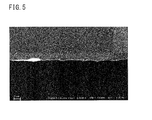
- FIG. 5 is a cross-sectional photograph of Comparative Example 3 by SEM, showing the ceramic substrate in a lower part and the metal plate in an upper part.
- the residual oxide is found at the metal plate side of the bonding interface between the ceramic substrate and the metal plate, as a row of a white part along the bonding interface; and it is found that the residual oxide exists with relatively large length.
- a reduction effect of the separation rate after hot-cold cycle is remarkable if the surface roughness Ra of the metal plate is 0.05 ⁇ m to 0.30 ⁇ m; and an anisotropy of the separation is reduced if a difference of the surface roughness between the rolling direction and the perpendicular direction is 0.10 ⁇ m or less, so that the reduction effect of the separation rate is further improved.
- the present invention can be applied on a case for manufacturing a power-module substrate which configures a power module controlling a large electric current and a large voltage; and it is possible to obtain a power-module substrate in which a separation at an end part of a metal plate can be prevented so that bonding reliability can be improved.
Landscapes
- Engineering & Computer Science (AREA)
- Chemical & Material Sciences (AREA)
- Ceramic Engineering (AREA)
- Materials Engineering (AREA)
- Mechanical Engineering (AREA)
- Manufacturing & Machinery (AREA)
- Microelectronics & Electronic Packaging (AREA)
- Structural Engineering (AREA)
- Organic Chemistry (AREA)
- Cooling Or The Like Of Semiconductors Or Solid State Devices (AREA)
- Ceramic Products (AREA)
Applications Claiming Priority (2)
| Application Number | Priority Date | Filing Date | Title |
|---|---|---|---|
| JP2012077401A JP5614423B2 (ja) | 2012-03-29 | 2012-03-29 | パワーモジュール用基板及びその製造方法 |
| PCT/JP2013/059001 WO2013146881A1 (ja) | 2012-03-29 | 2013-03-27 | パワーモジュール用基板及びその製造方法 |
Publications (3)
| Publication Number | Publication Date |
|---|---|
| EP2833397A1 true EP2833397A1 (de) | 2015-02-04 |
| EP2833397A4 EP2833397A4 (de) | 2015-11-11 |
| EP2833397B1 EP2833397B1 (de) | 2021-12-22 |
Family
ID=49260130
Family Applications (1)
| Application Number | Title | Priority Date | Filing Date |
|---|---|---|---|
| EP13768726.5A Active EP2833397B1 (de) | 2012-03-29 | 2013-03-27 | Substrat für leistungsmodul und herstellungsverfahren dafür |
Country Status (7)
| Country | Link |
|---|---|
| US (1) | US9862045B2 (de) |
| EP (1) | EP2833397B1 (de) |
| JP (1) | JP5614423B2 (de) |
| KR (1) | KR102004573B1 (de) |
| CN (1) | CN104170077B (de) |
| IN (1) | IN2014DN07986A (de) |
| WO (1) | WO2013146881A1 (de) |
Families Citing this family (9)
| Publication number | Priority date | Publication date | Assignee | Title |
|---|---|---|---|---|
| JP6287216B2 (ja) * | 2014-01-08 | 2018-03-07 | 三菱マテリアル株式会社 | ヒートシンク付パワーモジュール用基板の製造方法 |
| JP6287428B2 (ja) * | 2014-03-25 | 2018-03-07 | 三菱マテリアル株式会社 | ヒートシンク付パワーモジュール用基板の製造方法 |
| JP6323104B2 (ja) * | 2014-03-25 | 2018-05-16 | 三菱マテリアル株式会社 | ヒートシンク付パワーモジュール用基板の製造方法 |
| JP6159775B2 (ja) | 2014-10-31 | 2017-07-05 | 新日鐵住金ステンレス株式会社 | 耐排ガス凝縮水腐食性とろう付け性に優れたフェライト系ステンレス鋼及びその製造方法 |
| CN110809910B (zh) * | 2017-06-28 | 2022-11-25 | 京瓷株式会社 | 功率模块用基板以及功率模块 |
| CN113939095B (zh) | 2020-06-29 | 2023-02-10 | 比亚迪股份有限公司 | 一种陶瓷覆铜板及其制备方法 |
| CN116368610A (zh) | 2020-10-29 | 2023-06-30 | Ngk电子器件株式会社 | 半导体装置用基板 |
| JP2024132437A (ja) * | 2023-03-17 | 2024-10-01 | Dowaメタルテック株式会社 | 銅-セラミックス回路基板およびその製造方法 |
| CN117460174B (zh) * | 2023-12-25 | 2024-04-02 | 广州先艺电子科技有限公司 | 一种图案化amb陶瓷覆铜板的制备方法 |
Family Cites Families (15)
| Publication number | Priority date | Publication date | Assignee | Title |
|---|---|---|---|---|
| JPH06302927A (ja) * | 1993-04-15 | 1994-10-28 | Matsushita Electric Ind Co Ltd | セラミック配線基板とその製造方法及び電極ペースト |
| JP3890539B2 (ja) | 1996-04-12 | 2007-03-07 | Dowaホールディングス株式会社 | セラミックス−金属複合回路基板 |
| JPH11343178A (ja) * | 1998-06-02 | 1999-12-14 | Fuji Electric Co Ltd | 銅板と非酸化物セラミックスとの接合方法 |
| JP2001048671A (ja) * | 1999-08-13 | 2001-02-20 | Dowa Mining Co Ltd | 金属−セラミックス接合基板 |
| JP2001121287A (ja) * | 1999-10-21 | 2001-05-08 | Denki Kagaku Kogyo Kk | Al系金属用ろう材とそれを用いたセラミックス回路基板 |
| JP2002009212A (ja) | 2000-06-23 | 2002-01-11 | Denki Kagaku Kogyo Kk | 放熱構造体の製造方法 |
| US7601236B2 (en) * | 2003-11-28 | 2009-10-13 | Semiconductor Energy Laboratory Co., Ltd. | Method of manufacturing display device |
| JP4632116B2 (ja) | 2004-03-05 | 2011-02-16 | 日立金属株式会社 | セラミックス回路基板 |
| KR101108454B1 (ko) * | 2004-04-05 | 2012-01-31 | 미쓰비시 마테리알 가부시키가이샤 | Al/AlN 접합체, 전력 모듈용 기판 및 전력 모듈, 그리고 Al/AlN 접합체의 제조 방법 |
| JP4904916B2 (ja) | 2006-05-18 | 2012-03-28 | 三菱マテリアル株式会社 | パワーモジュール用基板およびパワーモジュール用基板の製造方法並びにパワーモジュール |
| JP4710798B2 (ja) * | 2006-11-01 | 2011-06-29 | 三菱マテリアル株式会社 | パワーモジュール用基板及びパワーモジュール用基板の製造方法並びにパワーモジュール |
| JP5056340B2 (ja) | 2007-10-22 | 2012-10-24 | トヨタ自動車株式会社 | 半導体モジュールの冷却装置 |
| CN102047413B (zh) * | 2008-06-06 | 2015-04-15 | 三菱综合材料株式会社 | 功率模块用基板、功率模块以及功率模块用基板的制造方法 |
| JP5245989B2 (ja) * | 2009-03-31 | 2013-07-24 | 三菱マテリアル株式会社 | パワーモジュール用基板の製造方法およびヒートシンク付パワーモジュール用基板の製造方法 |
| JP5548722B2 (ja) * | 2012-03-30 | 2014-07-16 | 三菱マテリアル株式会社 | ヒートシンク付パワーモジュール用基板、及び、ヒートシンク付パワーモジュール用基板の製造方法 |
-
2012
- 2012-03-29 JP JP2012077401A patent/JP5614423B2/ja active Active
-
2013
- 2013-03-27 EP EP13768726.5A patent/EP2833397B1/de active Active
- 2013-03-27 KR KR1020147029947A patent/KR102004573B1/ko not_active Expired - Fee Related
- 2013-03-27 US US14/388,953 patent/US9862045B2/en active Active
- 2013-03-27 WO PCT/JP2013/059001 patent/WO2013146881A1/ja not_active Ceased
- 2013-03-27 IN IN7986DEN2014 patent/IN2014DN07986A/en unknown
- 2013-03-27 CN CN201380015335.4A patent/CN104170077B/zh active Active
Also Published As
| Publication number | Publication date |
|---|---|
| EP2833397B1 (de) | 2021-12-22 |
| WO2013146881A1 (ja) | 2013-10-03 |
| EP2833397A4 (de) | 2015-11-11 |
| US20150328706A1 (en) | 2015-11-19 |
| JP5614423B2 (ja) | 2014-10-29 |
| CN104170077A (zh) | 2014-11-26 |
| KR20140142322A (ko) | 2014-12-11 |
| JP2013207236A (ja) | 2013-10-07 |
| IN2014DN07986A (de) | 2015-05-01 |
| US9862045B2 (en) | 2018-01-09 |
| KR102004573B1 (ko) | 2019-07-26 |
| CN104170077B (zh) | 2017-07-28 |
Similar Documents
| Publication | Publication Date | Title |
|---|---|---|
| EP2833397B1 (de) | Substrat für leistungsmodul und herstellungsverfahren dafür | |
| EP2911192B1 (de) | Substrat für ein strommodul mit einem kühlkörper, strommodul mit einem kühlkörper und verfahren zur herstellung des substrats für das strommodul mit einem kühlkörper | |
| CN109417056B (zh) | 铜-陶瓷接合体及绝缘电路基板 | |
| KR102272865B1 (ko) | 접합체, 히트 싱크가 부착된 파워 모듈용 기판, 히트 싱크, 접합체의 제조 방법, 히트 싱크가 부착된 파워 모듈용 기판의 제조 방법, 및 히트 싱크의 제조 방법 | |
| EP3590909B1 (de) | Isolierte leiterplatte mit kupfer-keramik-fügekörper, verfahren zur herstellung eines kupfer-keramik-fügekörpers und verfahren zur herstellung einer isolierten leiterplatte | |
| EP3632879B1 (de) | Keramische leiterplatte und sein herstellungsverfahren | |
| EP3136431B1 (de) | Substrat für leistungsmodule, substrat mit kühlkörper für leistungsmodule und leistungsmodul mit kühlkörper | |
| KR102130868B1 (ko) | 접합체, 파워 모듈용 기판, 및 히트 싱크가 부착된 파워 모듈용 기판 | |
| US12027434B2 (en) | Bonded body of copper and ceramic, insulating circuit substrate, bonded body of copper and ceramic production method, and insulating circuit substrate production method | |
| EP2833400B1 (de) | Leistungsmodulsubstrat mit kühlkörper und verfahren zur herstellung des leistungsmodulsubstrats mit dem kühlkörper | |
| KR20150056534A (ko) | 알루미늄 부재와 구리 부재의 접합 구조 | |
| CN101529588A (zh) | 功率模块用基板以及功率模块用基板的制造方法、及功率模块 | |
| CN114845977B (zh) | 铜-陶瓷接合体、及绝缘电路基板 | |
| KR20110015544A (ko) | 파워 모듈용 기판, 파워 모듈, 및 파워 모듈용 기판의 제조 방법 | |
| KR102462273B1 (ko) | 세라믹스/알루미늄 접합체, 파워 모듈용 기판, 및 파워 모듈 | |
| KR20170046649A (ko) | 접합체, 히트 싱크가 부착된 파워 모듈용 기판, 히트 싱크, 접합체의 제조 방법, 히트 싱크가 부착된 파워 모듈용 기판의 제조 방법, 및 히트 싱크의 제조 방법 | |
| EP3279936B1 (de) | Verfahren zur herstellung eines substrats für leistungsmodul mit kühlkörper | |
| JP5853727B2 (ja) | ヒートシンク付パワーモジュール用基板の製造方法 | |
| EP3960722B1 (de) | Kupfer-keramikverbundkörper, isolierschaltungssubstrat, verfahren zur herstellung eines kupfer-keramikverbundkörpers und verfahren zur herstellung eines isolierschaltungssubstrats | |
| JP6028352B2 (ja) | ヒートシンク付パワーモジュール用基板の製造方法 | |
| JP6152626B2 (ja) | パワーモジュール用基板の製造方法 | |
| US12089342B2 (en) | Insulated circuit board | |
| JP2025065004A (ja) | 銅/セラミックス接合体、および、絶縁回路基板 | |
| JP2013157524A (ja) | ヒートシンク付パワーモジュール用基板の製造方法およびパワーモジュール用基板 |
Legal Events
| Date | Code | Title | Description |
|---|---|---|---|
| PUAI | Public reference made under article 153(3) epc to a published international application that has entered the european phase |
Free format text: ORIGINAL CODE: 0009012 |
|
| 17P | Request for examination filed |
Effective date: 20141014 |
|
| AK | Designated contracting states |
Kind code of ref document: A1 Designated state(s): AL AT BE BG CH CY CZ DE DK EE ES FI FR GB GR HR HU IE IS IT LI LT LU LV MC MK MT NL NO PL PT RO RS SE SI SK SM TR |
|
| AX | Request for extension of the european patent |
Extension state: BA ME |
|
| DAX | Request for extension of the european patent (deleted) | ||
| RA4 | Supplementary search report drawn up and despatched (corrected) |
Effective date: 20151009 |
|
| RIC1 | Information provided on ipc code assigned before grant |
Ipc: H01L 23/473 20060101ALI20151005BHEP Ipc: H01L 23/13 20060101AFI20151005BHEP Ipc: C04B 37/02 20060101ALI20151005BHEP Ipc: H05K 1/02 20060101ALI20151005BHEP Ipc: H01L 23/373 20060101ALI20151005BHEP Ipc: H05K 3/38 20060101ALI20151005BHEP Ipc: B32B 18/00 20060101ALI20151005BHEP |
|
| STAA | Information on the status of an ep patent application or granted ep patent |
Free format text: STATUS: EXAMINATION IS IN PROGRESS |
|
| 17Q | First examination report despatched |
Effective date: 20190509 |
|
| RAP1 | Party data changed (applicant data changed or rights of an application transferred) |
Owner name: MITSUBISHI MATERIALS CORPORATION |
|
| RIC1 | Information provided on ipc code assigned before grant |
Ipc: H05K 1/03 20060101ALI20210727BHEP Ipc: H05K 1/02 20060101ALI20210727BHEP Ipc: B32B 18/00 20060101ALI20210727BHEP Ipc: C04B 37/02 20060101ALI20210727BHEP Ipc: H05K 3/38 20060101ALI20210727BHEP Ipc: H01L 23/473 20060101ALI20210727BHEP Ipc: H01L 23/373 20060101ALI20210727BHEP Ipc: H01L 23/13 20060101AFI20210727BHEP |
|
| GRAP | Despatch of communication of intention to grant a patent |
Free format text: ORIGINAL CODE: EPIDOSNIGR1 |
|
| STAA | Information on the status of an ep patent application or granted ep patent |
Free format text: STATUS: GRANT OF PATENT IS INTENDED |
|
| INTG | Intention to grant announced |
Effective date: 20210929 |
|
| GRAS | Grant fee paid |
Free format text: ORIGINAL CODE: EPIDOSNIGR3 |
|
| GRAA | (expected) grant |
Free format text: ORIGINAL CODE: 0009210 |
|
| STAA | Information on the status of an ep patent application or granted ep patent |
Free format text: STATUS: THE PATENT HAS BEEN GRANTED |
|
| AK | Designated contracting states |
Kind code of ref document: B1 Designated state(s): AL AT BE BG CH CY CZ DE DK EE ES FI FR GB GR HR HU IE IS IT LI LT LU LV MC MK MT NL NO PL PT RO RS SE SI SK SM TR |
|
| REG | Reference to a national code |
Ref country code: GB Ref legal event code: FG4D |
|
| REG | Reference to a national code |
Ref country code: CH Ref legal event code: EP |
|
| REG | Reference to a national code |
Ref country code: DE Ref legal event code: R096 Ref document number: 602013080495 Country of ref document: DE |
|
| REG | Reference to a national code |
Ref country code: AT Ref legal event code: REF Ref document number: 1457630 Country of ref document: AT Kind code of ref document: T Effective date: 20220115 |
|
| REG | Reference to a national code |
Ref country code: IE Ref legal event code: FG4D |
|
| REG | Reference to a national code |
Ref country code: LT Ref legal event code: MG9D |
|
| PG25 | Lapsed in a contracting state [announced via postgrant information from national office to epo] |
Ref country code: RS Free format text: LAPSE BECAUSE OF FAILURE TO SUBMIT A TRANSLATION OF THE DESCRIPTION OR TO PAY THE FEE WITHIN THE PRESCRIBED TIME-LIMIT Effective date: 20211222 Ref country code: LT Free format text: LAPSE BECAUSE OF FAILURE TO SUBMIT A TRANSLATION OF THE DESCRIPTION OR TO PAY THE FEE WITHIN THE PRESCRIBED TIME-LIMIT Effective date: 20211222 Ref country code: FI Free format text: LAPSE BECAUSE OF FAILURE TO SUBMIT A TRANSLATION OF THE DESCRIPTION OR TO PAY THE FEE WITHIN THE PRESCRIBED TIME-LIMIT Effective date: 20211222 Ref country code: BG Free format text: LAPSE BECAUSE OF FAILURE TO SUBMIT A TRANSLATION OF THE DESCRIPTION OR TO PAY THE FEE WITHIN THE PRESCRIBED TIME-LIMIT Effective date: 20220322 |
|
| REG | Reference to a national code |
Ref country code: NL Ref legal event code: MP Effective date: 20211222 |
|
| REG | Reference to a national code |
Ref country code: AT Ref legal event code: MK05 Ref document number: 1457630 Country of ref document: AT Kind code of ref document: T Effective date: 20211222 |
|
| PG25 | Lapsed in a contracting state [announced via postgrant information from national office to epo] |
Ref country code: SE Free format text: LAPSE BECAUSE OF FAILURE TO SUBMIT A TRANSLATION OF THE DESCRIPTION OR TO PAY THE FEE WITHIN THE PRESCRIBED TIME-LIMIT Effective date: 20211222 Ref country code: NO Free format text: LAPSE BECAUSE OF FAILURE TO SUBMIT A TRANSLATION OF THE DESCRIPTION OR TO PAY THE FEE WITHIN THE PRESCRIBED TIME-LIMIT Effective date: 20220322 Ref country code: LV Free format text: LAPSE BECAUSE OF FAILURE TO SUBMIT A TRANSLATION OF THE DESCRIPTION OR TO PAY THE FEE WITHIN THE PRESCRIBED TIME-LIMIT Effective date: 20211222 Ref country code: HR Free format text: LAPSE BECAUSE OF FAILURE TO SUBMIT A TRANSLATION OF THE DESCRIPTION OR TO PAY THE FEE WITHIN THE PRESCRIBED TIME-LIMIT Effective date: 20211222 Ref country code: GR Free format text: LAPSE BECAUSE OF FAILURE TO SUBMIT A TRANSLATION OF THE DESCRIPTION OR TO PAY THE FEE WITHIN THE PRESCRIBED TIME-LIMIT Effective date: 20220323 |
|
| PG25 | Lapsed in a contracting state [announced via postgrant information from national office to epo] |
Ref country code: NL Free format text: LAPSE BECAUSE OF FAILURE TO SUBMIT A TRANSLATION OF THE DESCRIPTION OR TO PAY THE FEE WITHIN THE PRESCRIBED TIME-LIMIT Effective date: 20211222 |
|
| PG25 | Lapsed in a contracting state [announced via postgrant information from national office to epo] |
Ref country code: SM Free format text: LAPSE BECAUSE OF FAILURE TO SUBMIT A TRANSLATION OF THE DESCRIPTION OR TO PAY THE FEE WITHIN THE PRESCRIBED TIME-LIMIT Effective date: 20211222 Ref country code: SK Free format text: LAPSE BECAUSE OF FAILURE TO SUBMIT A TRANSLATION OF THE DESCRIPTION OR TO PAY THE FEE WITHIN THE PRESCRIBED TIME-LIMIT Effective date: 20211222 Ref country code: RO Free format text: LAPSE BECAUSE OF FAILURE TO SUBMIT A TRANSLATION OF THE DESCRIPTION OR TO PAY THE FEE WITHIN THE PRESCRIBED TIME-LIMIT Effective date: 20211222 Ref country code: PT Free format text: LAPSE BECAUSE OF FAILURE TO SUBMIT A TRANSLATION OF THE DESCRIPTION OR TO PAY THE FEE WITHIN THE PRESCRIBED TIME-LIMIT Effective date: 20220422 Ref country code: ES Free format text: LAPSE BECAUSE OF FAILURE TO SUBMIT A TRANSLATION OF THE DESCRIPTION OR TO PAY THE FEE WITHIN THE PRESCRIBED TIME-LIMIT Effective date: 20211222 Ref country code: EE Free format text: LAPSE BECAUSE OF FAILURE TO SUBMIT A TRANSLATION OF THE DESCRIPTION OR TO PAY THE FEE WITHIN THE PRESCRIBED TIME-LIMIT Effective date: 20211222 Ref country code: CZ Free format text: LAPSE BECAUSE OF FAILURE TO SUBMIT A TRANSLATION OF THE DESCRIPTION OR TO PAY THE FEE WITHIN THE PRESCRIBED TIME-LIMIT Effective date: 20211222 |
|
| PG25 | Lapsed in a contracting state [announced via postgrant information from national office to epo] |
Ref country code: PL Free format text: LAPSE BECAUSE OF FAILURE TO SUBMIT A TRANSLATION OF THE DESCRIPTION OR TO PAY THE FEE WITHIN THE PRESCRIBED TIME-LIMIT Effective date: 20211222 Ref country code: AT Free format text: LAPSE BECAUSE OF FAILURE TO SUBMIT A TRANSLATION OF THE DESCRIPTION OR TO PAY THE FEE WITHIN THE PRESCRIBED TIME-LIMIT Effective date: 20211222 |
|
| REG | Reference to a national code |
Ref country code: DE Ref legal event code: R097 Ref document number: 602013080495 Country of ref document: DE |
|
| PG25 | Lapsed in a contracting state [announced via postgrant information from national office to epo] |
Ref country code: IS Free format text: LAPSE BECAUSE OF FAILURE TO SUBMIT A TRANSLATION OF THE DESCRIPTION OR TO PAY THE FEE WITHIN THE PRESCRIBED TIME-LIMIT Effective date: 20220422 |
|
| PLBE | No opposition filed within time limit |
Free format text: ORIGINAL CODE: 0009261 |
|
| STAA | Information on the status of an ep patent application or granted ep patent |
Free format text: STATUS: NO OPPOSITION FILED WITHIN TIME LIMIT |
|
| PG25 | Lapsed in a contracting state [announced via postgrant information from national office to epo] |
Ref country code: MC Free format text: LAPSE BECAUSE OF FAILURE TO SUBMIT A TRANSLATION OF THE DESCRIPTION OR TO PAY THE FEE WITHIN THE PRESCRIBED TIME-LIMIT Effective date: 20211222 Ref country code: DK Free format text: LAPSE BECAUSE OF FAILURE TO SUBMIT A TRANSLATION OF THE DESCRIPTION OR TO PAY THE FEE WITHIN THE PRESCRIBED TIME-LIMIT Effective date: 20211222 Ref country code: AL Free format text: LAPSE BECAUSE OF FAILURE TO SUBMIT A TRANSLATION OF THE DESCRIPTION OR TO PAY THE FEE WITHIN THE PRESCRIBED TIME-LIMIT Effective date: 20211222 |
|
| GBPC | Gb: european patent ceased through non-payment of renewal fee |
Effective date: 20220327 |
|
| 26N | No opposition filed |
Effective date: 20220923 |
|
| REG | Reference to a national code |
Ref country code: BE Ref legal event code: MM Effective date: 20220331 |
|
| PG25 | Lapsed in a contracting state [announced via postgrant information from national office to epo] |
Ref country code: LU Free format text: LAPSE BECAUSE OF NON-PAYMENT OF DUE FEES Effective date: 20220327 Ref country code: IE Free format text: LAPSE BECAUSE OF NON-PAYMENT OF DUE FEES Effective date: 20220327 Ref country code: GB Free format text: LAPSE BECAUSE OF NON-PAYMENT OF DUE FEES Effective date: 20220327 |
|
| PG25 | Lapsed in a contracting state [announced via postgrant information from national office to epo] |
Ref country code: SI Free format text: LAPSE BECAUSE OF FAILURE TO SUBMIT A TRANSLATION OF THE DESCRIPTION OR TO PAY THE FEE WITHIN THE PRESCRIBED TIME-LIMIT Effective date: 20211222 Ref country code: BE Free format text: LAPSE BECAUSE OF NON-PAYMENT OF DUE FEES Effective date: 20220331 |
|
| PG25 | Lapsed in a contracting state [announced via postgrant information from national office to epo] |
Ref country code: HU Free format text: LAPSE BECAUSE OF FAILURE TO SUBMIT A TRANSLATION OF THE DESCRIPTION OR TO PAY THE FEE WITHIN THE PRESCRIBED TIME-LIMIT; INVALID AB INITIO Effective date: 20130327 |
|
| PG25 | Lapsed in a contracting state [announced via postgrant information from national office to epo] |
Ref country code: MK Free format text: LAPSE BECAUSE OF FAILURE TO SUBMIT A TRANSLATION OF THE DESCRIPTION OR TO PAY THE FEE WITHIN THE PRESCRIBED TIME-LIMIT Effective date: 20211222 Ref country code: CY Free format text: LAPSE BECAUSE OF FAILURE TO SUBMIT A TRANSLATION OF THE DESCRIPTION OR TO PAY THE FEE WITHIN THE PRESCRIBED TIME-LIMIT Effective date: 20211222 |
|
| PGFP | Annual fee paid to national office [announced via postgrant information from national office to epo] |
Ref country code: IT Payment date: 20240320 Year of fee payment: 12 Ref country code: FR Payment date: 20240313 Year of fee payment: 12 |
|
| PG25 | Lapsed in a contracting state [announced via postgrant information from national office to epo] |
Ref country code: TR Free format text: LAPSE BECAUSE OF FAILURE TO SUBMIT A TRANSLATION OF THE DESCRIPTION OR TO PAY THE FEE WITHIN THE PRESCRIBED TIME-LIMIT Effective date: 20211222 |
|
| PGFP | Annual fee paid to national office [announced via postgrant information from national office to epo] |
Ref country code: CH Payment date: 20240401 Year of fee payment: 12 |
|
| PG25 | Lapsed in a contracting state [announced via postgrant information from national office to epo] |
Ref country code: MT Free format text: LAPSE BECAUSE OF FAILURE TO SUBMIT A TRANSLATION OF THE DESCRIPTION OR TO PAY THE FEE WITHIN THE PRESCRIBED TIME-LIMIT Effective date: 20211222 |
|
| PGFP | Annual fee paid to national office [announced via postgrant information from national office to epo] |
Ref country code: DE Payment date: 20250319 Year of fee payment: 13 |
|
| REG | Reference to a national code |
Ref country code: CH Ref legal event code: H13 Free format text: ST27 STATUS EVENT CODE: U-0-0-H10-H13 (AS PROVIDED BY THE NATIONAL OFFICE) Effective date: 20251023 |
|
| REG | Reference to a national code |
Ref country code: DE Ref legal event code: R079 Ref document number: 602013080495 Country of ref document: DE Free format text: PREVIOUS MAIN CLASS: H01L0023130000 Ipc: H10W0070680000 |
|
| PG25 | Lapsed in a contracting state [announced via postgrant information from national office to epo] |
Ref country code: FR Free format text: LAPSE BECAUSE OF NON-PAYMENT OF DUE FEES Effective date: 20250331 Ref country code: IT Free format text: LAPSE BECAUSE OF NON-PAYMENT OF DUE FEES Effective date: 20250327 |
|
| PG25 | Lapsed in a contracting state [announced via postgrant information from national office to epo] |
Ref country code: CH Free format text: LAPSE BECAUSE OF NON-PAYMENT OF DUE FEES Effective date: 20250331 |