EP2827165B1 - Magnetoresistance magnetic field gradient sensor - Google Patents
Magnetoresistance magnetic field gradient sensor Download PDFInfo
- Publication number
- EP2827165B1 EP2827165B1 EP13761465.7A EP13761465A EP2827165B1 EP 2827165 B1 EP2827165 B1 EP 2827165B1 EP 13761465 A EP13761465 A EP 13761465A EP 2827165 B1 EP2827165 B1 EP 2827165B1
- Authority
- EP
- European Patent Office
- Prior art keywords
- magnetoresistive
- magnetic field
- bridge
- gradiometer
- permanent magnets
- Prior art date
- Legal status (The legal status is an assumption and is not a legal conclusion. Google has not performed a legal analysis and makes no representation as to the accuracy of the status listed.)
- Active
Links
Images




Classifications
-
- G—PHYSICS
- G01—MEASURING; TESTING
- G01R—MEASURING ELECTRIC VARIABLES; MEASURING MAGNETIC VARIABLES
- G01R33/00—Arrangements or instruments for measuring magnetic variables
- G01R33/02—Measuring direction or magnitude of magnetic fields or magnetic flux
- G01R33/06—Measuring direction or magnitude of magnetic fields or magnetic flux using galvano-magnetic devices
- G01R33/09—Magnetoresistive devices
- G01R33/098—Magnetoresistive devices comprising tunnel junctions, e.g. tunnel magnetoresistance sensors
-
- G—PHYSICS
- G01—MEASURING; TESTING
- G01R—MEASURING ELECTRIC VARIABLES; MEASURING MAGNETIC VARIABLES
- G01R17/00—Measuring arrangements involving comparison with a reference value, e.g. bridge
-
- G—PHYSICS
- G01—MEASURING; TESTING
- G01R—MEASURING ELECTRIC VARIABLES; MEASURING MAGNETIC VARIABLES
- G01R33/00—Arrangements or instruments for measuring magnetic variables
- G01R33/02—Measuring direction or magnitude of magnetic fields or magnetic flux
- G01R33/022—Measuring gradient
-
- G—PHYSICS
- G01—MEASURING; TESTING
- G01R—MEASURING ELECTRIC VARIABLES; MEASURING MAGNETIC VARIABLES
- G01R33/00—Arrangements or instruments for measuring magnetic variables
- G01R33/02—Measuring direction or magnitude of magnetic fields or magnetic flux
- G01R33/06—Measuring direction or magnitude of magnetic fields or magnetic flux using galvano-magnetic devices
- G01R33/09—Magnetoresistive devices
- G01R33/093—Magnetoresistive devices using multilayer structures, e.g. giant magnetoresistance sensors
Definitions
- the present invention relates to magnetoresistive magnetic field gradient sensors, and in particular the use of magnetic tunnel junction magnetoresistive sensor elements to form a magnetoresistive magnetic field gradient sensor.
- Magnetic field sensors are commonly used in modern systems to measure the magnetic field, current, position, direction, and many other physical parameters.
- sensors for measuring magnetic field there are many different types of sensors for measuring magnetic field, and these commonly use the Hall Effect, an anisotropic magnetoresistance (AMR), or giant magnetoresistance (GMR) elements.
- AMR anisotropic magnetoresistance
- GMR giant magnetoresistance
- Hall Effect sensors generally have low sensitivity, and thus often use a flux concentrator to increase the sensitivity. Flux concentrators increase the size and weight of the sensor, and can decrease the linearity of the sensor. Moreover, Hall elements generally have high power consumption. Although AMR elements have much higher sensitivity than Hall elements, they suffer from narrow linear range, and they need to be reset using a set / reset coil. The reset operation, resulting increases the complexity of the manufacturing process; the coil increases the size of the sensor; and, the power consumption also increased by the reset operation.
- Multilayer GMR sensor elements have higher sensitivity than AMR, but their linear range is low, and unless they are biased by a permanent magnet, the response curve of only provide a unipolar measurement of the magnetic field gradient, so that a bipolar magnetic field gradient cannot be measured.
- Magnetic tunnel junction (MTJ) elements in recent years have been gaining acceptance as magnetoresistive sensors in industrial applications. They are multilayer devices that utilize the tunnel magnetoresistance effect (TMR) for measuring the magnetic field, and these elements possess a larger rate of resistance change than AMR or GMR elements.
- TMR tunnel magnetoresistance effect
- MTJ elements Compared to the Hall Effect sensors, MTJ elements have superior temperature stability, higher sensitivity, lower power consumption, better linearity, and no need for flux concentrators; with respect to AMR sensors they have improved temperature stability, higher sensitivity, wider linear range, and no need for a set/reset coil structure; compared to GMR sensors they have better temperature stability, higher sensitivity, lower power consumption, and wider linear range.
- MTJ elements have high sensitivity, when used to detect weak field gradients the MTJ element can be disturbed by strong magnetic fields, and the high sensitivity MTJ elements are not easily amenable to low-cost mass production.
- the sensor yield depends on the offset value output from MTJ magnetoresistive element constituting the magnetoresistive bridge, because MTJ elements are often difficult to match on the different arms of the bridge.
- the manufacturing process for fully single-chip MTJ sensor bridges is very complicated.
- US20050073301A1 discloses a sensor element and gradiometer assemblage, use thereof for measuring magnetic field gradients, and method therefor.
- US20040046624A1 discloses a magneto-resistive layer arrangement and gradiometer with said layer arrangement.
- US6956366B2 discloses an arrangement for determining the position of a motion sensor element influencing the formation of a magnetic field of a working magnet along its motion coordinate.
- CN102226835A discloses a single-chip double-axis magnetic field sensor and preparation method thereof.
- the present invention utilizes MTJ elements as the sensing elements in a magnetoresistive magnetic field gradiometer, which results in the advantages of high sensitivity, wide linear range, low power consumption, small volume, and good temperature performance.
- magnetoresistive bridge is a full-bridge, comprising a pair of the half-bridges connected in parallel, wherein the magnetoresistive arms have the same sensing direction, the arms opposite to each other in the circuit diagram are in the same spatial location on the substrate and the arms adjacent to each other in the circuit diagram are in different spatial locations on the substrate, such that the magnetoresistive bridge is configured for detecting a magnetic field gradient.
- the magnitude of the magnetization and direction of the of the permanent magnet are selected in order to provide the required output performance of the magnetoresistive magnetic field gradiometer.
- the magnitude of the magnetization and direction of the of the permanent magnet are selected in order to provide the required output performance of the magnetoresistive magnetic field gradiometer Adopting the above described features, the present invention will have good external DC magnetic field insensitivity, high gradient sensitivity, wide linear operating range, low power dissipation, small size, and good thermal performance.
- FIG. 1 is a drawing that illustrates the function of the various layers in an MTJ element.
- a MTJ element 1 generally includes an upper layer of a ferromagnetic or synthetic antiferromagnetic (SAF) 5, a lower ferromagnetic SAF layer 3, and a tunnel barrier 4 between the two ferromagnetic layers.
- the upper ferromagnetic (SAF layer) constitutes the magnetic free layer 5, in which the magnetic moment is free to change direction in response to the external magnetic field 7.
- the lower ferromagnetic (SAF layer) 3 is a fixed magnetic layer, because its magnetic moment direction 8 is rigidly fixed in one direction, so under normal conditions will not change.
- the rigidly fixed ferromagnetic layer (SAF layer) 3 is called the pinned layer.
- the pinned layer is usually adjacent to an antiferromagnetic layer 2.
- the MTJ stack is usually deposited on top of an electrically conductive bottom electrode layer 9, and the MTJ structure is often capped with a conducting top electrode layer 6.
- the value of the resistance 12 measured between the top 6 and bottom 9 electrode layers of the MTJ is representative of the relative orientation of magnetic moments of the free layer 5 and the pinned layer 3.
- the resistance 12 of the MTJ element 1 is low.
- the resistance of the MTJ element 1 may be made to vary linearly between the high resistance state and the low resistance state as the external magnetic field is varied.
- the bottom electrode layer 9 and the top electrode layer 6 are in direct electrical contact respectively with the free layer 5 and antiferromagnetic layer 2.
- the electrode layers are generally composed of non-magnetic conductive materials capable of carrying current to the ohmmeter 34.
- Ohmmeter 34 applies a known current (voltage) through the entire tunnel junction, and a voltage (or current) is measured.
- the tunnel barrier layer 4 provides most of the resistance of the device, on the order of about 1000 ohms and the resistance of all other conductors is about 10 ohms.
- the bottom electrode layer 9 is deposited on top of the insulating layer 10, which is in turn deposited on substrate 11, and insulating layer 10 is thicker than electrode layer 9, and they are composed of different materials.
- the substrate material is typically silicon, quartz, heat-resistant glass, GaAs, AlTiC or any other material capable of being provided as a smooth wafer. Because of the ease of processing integrated circuits (although such magnetic sensors may not always need circuitry) silicon is usually the best choice.
- Figure 2 shows the linear response of a GMR or MTJ magnetoresistive element.
- the output curve 13 When saturated, the output curve 13 will be in either the low resistance 14 R L or the high resistance 15 R H state.
- Response curve 13 in the area between the saturation fields varies linearly with the external magnetic field 19 (H).
- the external magnetic field 19 is applied parallel to the sensing axis 23.
- the magnetic field is negative (-H).
- the offset value is often referred to as "orange peel coupling" or “Neel coupling,” the typical value of this offset is usually between 1 and 40 Oe. It depends on the roughness of the MTJ element, making it dependent on materials and manufacturing processes.
- H S is the saturation field.
- H S is defined as the intersection between the linear region and the positive and negative saturation values, where the position is asymmetric due to H o .
- Figure 2 shows the ideal magnetoresistive response curve.
- the magnetoresistance R changes perfectly linearly with respect to applied field H, and there is no hysteresis (in actuality, the magnetoresistance shows a lag phenomenon, which is referred to as hysteresis; the magnetoresistive response curve for a full loop, often the hysteresis of common magnetoresistive materials is small, such that the response curve can be practically regarded as a straight line).
- the transfer curve 13 will not be truly linear.
- MTJ elements 1 can be connected in series to form an equivalent MTJ magnetoresistor with increased sensitivity, with a reduction of 1/F noise (which decreases as the number of MTJ elements 1 in series increases), while improving the ESD performance.
- the more complicated MTJ element array 20 is used as a magnetoresistive arm.
- the MTJ element 1 sits between the bottom electrode 9 and the top electrode 6 in a sandwich structure, wherein the current flows perpendicularly through the MTJ element 21 and flows horizontally in the top electrode layer 6 and the bottom electrode layer 9.
- Bottom electrode 9 is on the top of insulating layer 10, and insulating layer 10 is on the top of the substrate 11.
- a wire bond pad sits at the end of each string of MTJ elements making up a magnetoresistive arm. This is where other magnetoresistive arms or where the ohmmeter 34 or other electrical circuit components may be connected.
- the direction of current flow through the MTJ magnetoresistive arm 20 does not affect the value of the magnetoresistance or the resistance.
- the value of the resistance can be changed by changing the number of MTJ elements 1 in the magnetoresistive arm 20.
- Abridge circuit is often used to change the output resistance to a voltage than can be easily amplified. It can reduce the sensor noise, improve common mode rejection, reduce temperature drift and improve other deficiencies.
- the above mentioned MTJ arm 20 can be made into a bridge circuit.
- an MTJ element 1 is placed between two permanent magnets 22.
- Permanent magnets 22 have a gap 38 (Gap) between them, a width (W) 39, a thickness (1) 40 and length (L y ) 41.
- Permanent magnet 22 is designed to provide a cross-bias field (H cross ) 27 perpendicular to the sensitive axis 23 of the gradiometer.
- the magnetization of the permanent magnets 22 can be set by applying a large magnetic field, and the resulting field distribution 43 of the permanent magnets 22 is shown in Figure 5 .
- the magnetic field emanating from the edge 35 of the permanent magnets 22 is considered to arise from magnetic charges that form as a result of boundary conditions as shown schematically in Figure 6 .
- Equation 4 is a function of the width W 39 and gap G 38 shown in Figure 4 , so the saturation field of the MTJ element 1 can be changed by changing the dimensions of permanent magnets 22.
- H cross H mag sin ⁇ sns
- MTJ element 1 is generally patterned into a shape in order to provide shape anisotropy H k .
- the common shapes are long ellipse, long rectangle, rhomboid, etc.
- the response curve of the MTJ element can be modified.
- FIG. 7 schematically shows a half-bridge gradiometer configuration.
- the two MTJ elements R1 and R2 have the same sensing direction, configured as a half-bridge, the magnetoresistors are deposited on substrate 11 and insulating layer 10 which has electrical contacts, allowing for the formation of the gradiometer.
- the bridge electrical contacts There are many ways to connect to the bridge electrical contacts. These include the typical structure: integrated in-chip connections, wire-bonding, and solder-bumping.
- the permanent magnets 22 are tilted with respect to the MTJ elements 20. Between the two wire bond pads 28 and 29 a constant bias voltage V bias is applied.
- Arrow 8 represents the magnetization direction of the pinning layers 3 of the MTJ elements 20, wire-bond pad 30 provides the gradiometer output V OUT .
- the fields H CM and H dM are the common mode and differential mode output field values.
- the output does not change with H CM , it is only sensitive to the external magnetic field gradient, and this makes it insensitive to external magnetic field interference.
- V OUT R 2 ⁇ S R 2 H dM R 1 + S R 1 H dM + R 2 ⁇ S R 2 H dM ⁇ R 2 R 1 + R 2 V bias ,
- the half-bridge gradiometer in differential mode only responds to a gradient magnetic field, and outputs a signal proportional to it, but also has good magnetic field anti-interference capability.
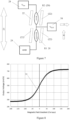
- the measurement results of the described half-bridge gradiometer are shown in Figure 8 .
- the horizontal axis represents the gradient magnetic field. Because they are located at different locations, and the applied magnetic field has a gradient, the strength of the magnetic fields H1 and H2 at resistors R1 and R2 is different.
- CMRR 20 log S CM S dM
- CMRR is better than 40dB.
- FIG 9 shows the circuit diagram of a full-bridge magnetic field gradiometer
- Figure 10 shows the physical layout of the full bridge MTJ magnetic field gradiometer.
- each of the four magnetoresistive arms R1, R2, R3, R4 in the full bridge has the same sensitive direction.
- the magnetoresistors are deposited on the insulated substrate 10, 11 which is prepared with electrical contacts that can be used to electrically connect them.
- R1 and R4 are in same physical location on the chip, R2 and R3 are in the same physical location on the chip, all magnetoresistive arms in the bridge have the same sensitive direction, permanent magnets 22 are tilted and set around the MTJ elements 20, a bias voltage V bias is applied between bond-pads 28 and 29, the gradient of the external magnetic field H is measured along the sensitive direction 23, along the field direction the different pairs of MTJ magnetoresistive elements R1 and R2 (R3 and R4) show a different resistance change, arrow 8 shows the pinned layer magnetization direction for all four MTJ elements 20,
- the output terminals of the device 32 and 33 are representative of the voltage difference (V2-V1) and are the V OUT .
- V OUT only responds to the differential mode magnetic field H dM .
- V 1 ⁇ S R 2 ⁇ H dM 2 R 2
- V bias ⁇ S R H dM 2 R V bias
- V 2 R 4 + S R 4 H dM R 4 + S R 4 H dM + R 3 ⁇ S R 3 H dM ⁇ R 4 R 3 + R 4 V bias ⁇
- R is the resistance value of the MTJ elements 20
- S R is the sensitivity of the magnetoresistive elements. It can be shown that the full- and half-bridge magnetic field gradiometers have the same insensitivity to common mode magnetic fields, but the full-bridge has twice the sensitivity of the half-bridge magnetic field gradiometer. The typical output response of a full-bridge magnetic field gradiometer is shown in Figure 11 .
- the above mentioned half and full-bridge gradiometers can be prepared on single substrate using the same process steps. For this reason they can be called single-chip magnetoresistive magnetic field gradiometers. They are compatible with various different packaging techniques and can also be made multi-chip. For example, the magnetoresistive elements can be prepared on the same substrate using the same process steps, but then diced into separate chips that are electrically connected, resulting in full or half-bridge gradiometer devices. Whether single or multi-chip packaging is used, the external bond pads of the bridges may or may not be connected to an ASIC both of which would be placed on a lead frame, electrically connected to the output pins of the lead frame, and then encapsulated to form the packaged device.
Landscapes
- Physics & Mathematics (AREA)
- General Physics & Mathematics (AREA)
- Condensed Matter Physics & Semiconductors (AREA)
- Measuring Magnetic Variables (AREA)
- Hall/Mr Elements (AREA)
Description
- The present invention relates to magnetoresistive magnetic field gradient sensors, and in particular the use of magnetic tunnel junction magnetoresistive sensor elements to form a magnetoresistive magnetic field gradient sensor.
- Magnetic field sensors are commonly used in modern systems to measure the magnetic field, current, position, direction, and many other physical parameters. In the prior art, there are many different types of sensors for measuring magnetic field, and these commonly use the Hall Effect, an anisotropic magnetoresistance (AMR), or giant magnetoresistance (GMR) elements.
- Hall Effect sensors generally have low sensitivity, and thus often use a flux concentrator to increase the sensitivity. Flux concentrators increase the size and weight of the sensor, and can decrease the linearity of the sensor. Moreover, Hall elements generally have high power consumption. Although AMR elements have much higher sensitivity than Hall elements, they suffer from narrow linear range, and they need to be reset using a set / reset coil. The reset operation, resulting increases the complexity of the manufacturing process; the coil increases the size of the sensor; and, the power consumption also increased by the reset operation. Multilayer GMR sensor elements have higher sensitivity than AMR, but their linear range is low, and unless they are biased by a permanent magnet, the response curve of only provide a unipolar measurement of the magnetic field gradient, so that a bipolar magnetic field gradient cannot be measured.
- Magnetic tunnel junction (MTJ) elements in recent years have been gaining acceptance as magnetoresistive sensors in industrial applications. They are multilayer devices that utilize the tunnel magnetoresistance effect (TMR) for measuring the magnetic field, and these elements possess a larger rate of resistance change than AMR or GMR elements. Compared to the Hall Effect sensors, MTJ elements have superior temperature stability, higher sensitivity, lower power consumption, better linearity, and no need for flux concentrators; with respect to AMR sensors they have improved temperature stability, higher sensitivity, wider linear range, and no need for a set/reset coil structure; compared to GMR sensors they have better temperature stability, higher sensitivity, lower power consumption, and wider linear range.
- Although MTJ elements have high sensitivity, when used to detect weak field gradients the MTJ element can be disturbed by strong magnetic fields, and the high sensitivity MTJ elements are not easily amenable to low-cost mass production. The sensor yield depends on the offset value output from MTJ magnetoresistive element constituting the magnetoresistive bridge, because MTJ elements are often difficult to match on the different arms of the bridge. The manufacturing process for fully single-chip MTJ sensor bridges is very complicated.
-
US20050073301A1 discloses a sensor element and gradiometer assemblage, use thereof for measuring magnetic field gradients, and method therefor.US20040046624A1 discloses a magneto-resistive layer arrangement and gradiometer with said layer arrangement.US6956366B2 discloses an arrangement for determining the position of a motion sensor element influencing the formation of a magnetic field of a working magnet along its motion coordinate.CN102226835A discloses a single-chip double-axis magnetic field sensor and preparation method thereof. - In order to solve these problems, the present invention utilizes MTJ elements as the sensing elements in a magnetoresistive magnetic field gradiometer, which results in the advantages of high sensitivity, wide linear range, low power consumption, small volume, and good temperature performance.
- There is provided a magnetoresistive magnetic field gradiometer sensor in accordance with the appended claims.
- Preferably, magnetoresistive bridge is a full-bridge, comprising a pair of the half-bridges connected in parallel, wherein the magnetoresistive arms have the same sensing direction, the arms opposite to each other in the circuit diagram are in the same spatial location on the substrate and the arms adjacent to each other in the circuit diagram are in different spatial locations on the substrate, such that the magnetoresistive bridge is configured for detecting a magnetic field gradient.
- Preferably, the magnitude of the magnetization and direction of the of the permanent magnet are selected in order to provide the required output performance of the magnetoresistive magnetic field gradiometer.
- Preferably, the magnitude of the magnetization and direction of the of the permanent magnet are selected in order to provide the required output performance of the magnetoresistive magnetic field gradiometer
Adopting the above described features, the present invention will have good external DC magnetic field insensitivity, high gradient sensitivity, wide linear operating range, low power dissipation, small size, and good thermal performance. -
-
Figure 1 is a schematic view of a MTJ magnetoresistive element. -
Figure 2 illustrates the linear response of a MTJ magnetoresistive element. -
Figure 3 illustrates a plurality of MTJ elements connected in series to form an equivalent MTJmagnetoresistive element 20. -
Figure 4 illustrates the relative position ofMTJ elements 1 andpermanent magnets 22. -
Figure 5 is a cross-sectional view aMTJ element 1 and thepermanent magnet 22 as shown in shown inFIG 4 , showing the flux distribution of the magnetic field. -
Figure 6 is a schematic view of thepermanent magnet 22 and thevarious angles 23 relative to the sensing direction used to control the MTJ element offset and saturation field strength. -
Figure 7 is a schematic diagram of a half-bridge magnetic field gradiometer. -
Figure 8 illustrates the output response of a half-bridge magnetic field gradiometer sensor. -
Figure 9 shows the circuit diagram of a full-bridge magnetic field gradiometer sensor. -
Figure 10 is a schematic diagram of a full-bridge magnetic field gradiometer. -
Figure 11 illustrates the output response of a full-bridge magnetic field gradiometer sensor. -
Figure 1 is a drawing that illustrates the function of the various layers in an MTJ element. AMTJ element 1 generally includes an upper layer of a ferromagnetic or synthetic antiferromagnetic (SAF) 5, a lowerferromagnetic SAF layer 3, and a tunnel barrier 4 between the two ferromagnetic layers. In this configuration, the upper ferromagnetic (SAF layer) constitutes the magneticfree layer 5, in which the magnetic moment is free to change direction in response to the externalmagnetic field 7. The lower ferromagnetic (SAF layer) 3 is a fixed magnetic layer, because itsmagnetic moment direction 8 is rigidly fixed in one direction, so under normal conditions will not change. Usually the rigidly fixed ferromagnetic layer (SAF layer) 3 is called the pinned layer. The pinned layer is usually adjacent to anantiferromagnetic layer 2. The MTJ stack is usually deposited on top of an electrically conductivebottom electrode layer 9, and the MTJ structure is often capped with a conductingtop electrode layer 6. The value of theresistance 12 measured between thetop 6 andbottom 9 electrode layers of the MTJ is representative of the relative orientation of magnetic moments of thefree layer 5 and thepinned layer 3. When themagnetization direction 7 offree layer 5 and themagnetization direction 8 ofpinned layer 3 are parallel theresistance 12 of theMTJ element 1 is low. When themagnetization direction 7 offree layer 5 and themagnetization direction 8 ofpinned layer 3 are antiparallel theresistance 12 of theMTJ element 1 is high. By known techniques, the resistance of theMTJ element 1 may be made to vary linearly between the high resistance state and the low resistance state as the external magnetic field is varied. - The
bottom electrode layer 9 and thetop electrode layer 6 are in direct electrical contact respectively with thefree layer 5 andantiferromagnetic layer 2. The electrode layers are generally composed of non-magnetic conductive materials capable of carrying current to theohmmeter 34.Ohmmeter 34 applies a known current (voltage) through the entire tunnel junction, and a voltage (or current) is measured. Typically, the tunnel barrier layer 4 provides most of the resistance of the device, on the order of about 1000 ohms and the resistance of all other conductors is about 10 ohms. Thebottom electrode layer 9 is deposited on top of theinsulating layer 10, which is in turn deposited onsubstrate 11, andinsulating layer 10 is thicker thanelectrode layer 9, and they are composed of different materials. The substrate material is typically silicon, quartz, heat-resistant glass, GaAs, AlTiC or any other material capable of being provided as a smooth wafer. Because of the ease of processing integrated circuits (although such magnetic sensors may not always need circuitry) silicon is usually the best choice. -
Figure 2 shows the linear response of a GMR or MTJ magnetoresistive element. When saturated, theoutput curve 13 will be in either the low resistance 14 RL or the high resistance 15 RH state.Response curve 13 in the area between the saturation fields varies linearly with the external magnetic field 19 (H). The externalmagnetic field 19 is applied parallel to thesensing axis 23. When the pinnedlayer 3magnetization 8 is oriented antiparallel to thesensitive axis 23, the magnetic field is negative (-H). When themagnetization direction 8 of thepinned layer 3 is parallel to themagnetization direction 7 of thefree layer 5, thetransfer curve 13 is in a low-resistance state; when themagnetization direction 8 of thepinned layer 3 is anti-parallel to themagnetization direction 7 of thefree layer 5, thetransfer curve 13 is in a high-resistance state. In between, theoutput curve 13 is linearly dependent on the relative magnetization angle of pinnedlayer 3 andfree layer 5. As manufactured (i.e. without magnetic field biasing), theoutput curve 13 is usually not symmetric about H = 0. Typically the saturation fields 17 and 18 are offset with respect to the H = 0point 16, such that the low-resistance state RL saturation point is closer to H = 0. The offset value is often referred to as "orange peel coupling" or "Neel coupling," the typical value of this offset is usually between 1 and 40 Oe. It depends on the roughness of the MTJ element, making it dependent on materials and manufacturing processes. - As shown in
Figure 2 , between the saturatedregions 
- Herein, HS is the saturation field. HS is defined as the intersection between the linear region and the positive and negative saturation values, where the position is asymmetric due to Ho.
-
Figure 2 shows the ideal magnetoresistive response curve. In the ideal state, the magnetoresistance R changes perfectly linearly with respect to applied field H, and there is no hysteresis (in actuality, the magnetoresistance shows a lag phenomenon, which is referred to as hysteresis; the magnetoresistive response curve for a full loop, often the hysteresis of common magnetoresistive materials is small, such that the response curve can be practically regarded as a straight line). In real applications of magnetoresistive sensors, due to magnetic sensor design constraints and material defects, thetransfer curve 13 will not be truly linear. - As shown in
Figure 3 , because of their small size,several MTJ elements 1 can be connected in series to form an equivalent MTJ magnetoresistor with increased sensitivity, with a reduction of 1/F noise (which decreases as the number ofMTJ elements 1 in series increases), while improving the ESD performance. The more complicatedMTJ element array 20 is used as a magnetoresistive arm. TheMTJ element 1 sits between thebottom electrode 9 and thetop electrode 6 in a sandwich structure, wherein the current flows perpendicularly through theMTJ element 21 and flows horizontally in thetop electrode layer 6 and thebottom electrode layer 9.Bottom electrode 9 is on the top of insulatinglayer 10, and insulatinglayer 10 is on the top of thesubstrate 11. A wire bond pad sits at the end of each string of MTJ elements making up a magnetoresistive arm. This is where other magnetoresistive arms or where theohmmeter 34 or other electrical circuit components may be connected. The direction of current flow through theMTJ magnetoresistive arm 20 does not affect the value of the magnetoresistance or the resistance. The value of the resistance can be changed by changing the number ofMTJ elements 1 in themagnetoresistive arm 20. - Abridge circuit is often used to change the output resistance to a voltage than can be easily amplified. It can reduce the sensor noise, improve common mode rejection, reduce temperature drift and improve other deficiencies. The above mentioned
MTJ arm 20 can be made into a bridge circuit. - As shown in
Figure 4 , anMTJ element 1 is placed between twopermanent magnets 22.Permanent magnets 22 have a gap 38 (Gap) between them, a width (W) 39, a thickness (1) 40 and length (Ly) 41.Permanent magnet 22 is designed to provide a cross-bias field (Hcross) 27 perpendicular to thesensitive axis 23 of the gradiometer. The magnetization of thepermanent magnets 22 can be set by applying a large magnetic field, and the resultingfield distribution 43 of thepermanent magnets 22 is shown inFigure 5 . - The magnetic field emanating from the
edge 35 of thepermanent magnets 22 is considered to arise from magnetic charges that form as a result of boundary conditions as shown schematically inFigure 6 . The amount of magnetic charge depends on the magnitude Mr and direction θmag 37 of the magnetic moment, and the associated angle of orientation of thepermanent magnets θ sns 44 as:
- Additionally, the magnetic field resulting from the distribution of magnetic charges can be defined as:

- When θmag = θref = π/2, the magnetic field at
MTJ element 1 only depends on remnant moment MR as described by the following equation:
- Equation 4 is a function of the
width W 39 andgap G 38 shown inFigure 4 , so the saturation field of theMTJ element 1 can be changed by changing the dimensions ofpermanent magnets 22. - Along the direction perpendicular to the
sensitive direction 23 of the MTJ element,permanent magnets 22 produce a bias field for the magnetoresistive element,
- Parallel to the
sensitive direction 23 of the MTJ element, the magnetic field of thepermanent magnet 22 is
- As can be seen from above, by adjusting the thickness t of the permanent magnet, the angles of the
permanent magnet θ mag 37 andθ sns 44, it is possible to change Hoff, in order to compensate the MTJ element against the Neel coupling field H0, thereby modifying the output characteristics and improving performance. On the other hand, it is also possible to adjust Hcross, to change the saturation field of the MTJ element, thereby adjusting the sensitivity. - By setting the
permanent magnets 22 at anangle θ sns 44 with respect to thesensing axis 23, it is possible to simultaneously produceH cross 27 andH off 26 fields, in order to set the MTJ element saturation field, at the same time cancelling the Neel coupling, to center the response curve of the MTJ element around zero field; this method will optimize the symmetry of the output response of the bridge, reduce effective Neel coupling and set desired sensitivity. In addition, setting the remnant magnetization Mr at angle θmag 37 with respect to thesensing axis 23 after preparation of the gradiometer chip, permits fine tuning of the device to optimize symmetry, allowing further improvement manufacturing yield. -
MTJ element 1 is generally patterned into a shape in order to provide shape anisotropy Hk. The common shapes are long ellipse, long rectangle, rhomboid, etc. With regard to this, theMTJ element 1 will have a saturation field Hs given by:
- A single MTJ element
magnetoresistive response curve 13 as herein described has a sensitivity of:
- By changing the shape of the permanent magnets and the MTJ elements the response curve of the MTJ element can be modified.
-
Figure 7 schematically shows a half-bridge gradiometer configuration. As shown inFigure 7 , the two MTJ elements R1 and R2 have the same sensing direction, configured as a half-bridge, the magnetoresistors are deposited onsubstrate 11 and insulatinglayer 10 which has electrical contacts, allowing for the formation of the gradiometer. There are many ways to connect to the bridge electrical contacts. These include the typical structure: integrated in-chip connections, wire-bonding, and solder-bumping. Thepermanent magnets 22 are tilted with respect to theMTJ elements 20. Between the twowire bond pads 28 and 29 a constant bias voltage Vbias is applied. A gradient in external magnetic field H along thesensing direction 23, causes a different magnetic field to be produced at MTJ elements R1 and R2 causing them to show different resistance values.Arrow 8 represents the magnetization direction of the pinninglayers 3 of theMTJ elements 20, wire-bond pad 30 provides the gradiometer output VOUT. When deposited on the samesubstrate MTJ elements 20 usually have about the same resistance, although it is not possible to guarantee a perfect match. There is often some slight difference between the two MTJ elements R1 and R2, such that we may define different effective magnetic fields H1 and H2, wherein H1 and H2 can be written:
and
- The fields HCM and HdM are the common mode and differential mode output field values.
- Ideally, R1 = R2, SR1 = SR2, and MTJ elements R1 and R2 are consistently the same, biased with half-bridge bias voltage Vbias, then for a common mode magnetic field HCM, the half-bridge output voltage is VOUT 30:

- Setting Vbias = 1V results in a common mode sensitivity of SCM = dV1/dHCM = 0.
- The output does not change with HCM, it is only sensitive to the external magnetic field gradient, and this makes it insensitive to external magnetic field interference.
- For the differential mode HdM, we can write:

- Ideally, sensitivities SR1=SR2, R1=R2 such that:

- So it can be observed that the gradiometer output changes in response to a differential mode field HdM change, when biased Vbias = 1V, the sensitivity is

- As can be seen from the above equation, the half-bridge gradiometer in differential mode only responds to a gradient magnetic field, and outputs a signal proportional to it, but also has good magnetic field anti-interference capability. The measurement results of the described half-bridge gradiometer are shown in
Figure 8 . Unlike the case of an ordinary half-bridge, the horizontal axis represents the gradient magnetic field. Because they are located at different locations, and the applied magnetic field has a gradient, the strength of the magnetic fields H1 and H2 at resistors R1 and R2 is different. - Small differences in R1 and R2, make small differences in sensitivities SR1 and SR2, and this causes a response to a common mode magnetic field HCM. Still, the common mode sensitivity is much smaller than the differential mode sensitivity, and the sensitivity to the undesired common mode response can be quantified as a common mode rejection ratio CMRR:

- With good process capability, CMRR is better than 40dB.
-
Figure 9 shows the circuit diagram of a full-bridge magnetic field gradiometer, andFigure 10 shows the physical layout of the full bridge MTJ magnetic field gradiometer. As shown inFigure 10 , each of the four magnetoresistive arms R1, R2, R3, R4 in the full bridge has the same sensitive direction. The magnetoresistors are deposited on theinsulated substrate Figure 10 , in the full bridge structure R1 and R4 are in same physical location on the chip, R2 and R3 are in the same physical location on the chip, all magnetoresistive arms in the bridge have the same sensitive direction,permanent magnets 22 are tilted and set around theMTJ elements 20, a bias voltage Vbias is applied between bond-pads sensitive direction 23, along the field direction the different pairs of MTJ magnetoresistive elements R1 and R2 (R3 and R4) show a different resistance change,arrow 8 shows the pinned layer magnetization direction for all fourMTJ elements 20, The output terminals of thedevice - Ideally, the output VOUT only responds to the differential mode magnetic field HdM. For the differential mode, the response can be written:


- Under ideal conditions, R1 = R2 = R3 = R4, and SR1 = SR2 = SR3 = SR4 = SR, such that:

- Wherein, R is the resistance value of the
MTJ elements 20, and SR is the sensitivity of the magnetoresistive elements. It can be shown that the full- and half-bridge magnetic field gradiometers have the same insensitivity to common mode magnetic fields, but the full-bridge has twice the sensitivity of the half-bridge magnetic field gradiometer. The typical output response of a full-bridge magnetic field gradiometer is shown inFigure 11 . - The above mentioned half and full-bridge gradiometers can be prepared on single substrate using the same process steps. For this reason they can be called single-chip magnetoresistive magnetic field gradiometers. They are compatible with various different packaging techniques and can also be made multi-chip. For example, the magnetoresistive elements can be prepared on the same substrate using the same process steps, but then diced into separate chips that are electrically connected, resulting in full or half-bridge gradiometer devices. Whether single or multi-chip packaging is used, the external bond pads of the bridges may or may not be connected to an ASIC both of which would be placed on a lead frame, electrically connected to the output pins of the lead frame, and then encapsulated to form the packaged device.
- The above description describes several different specific implementations of the invention, obviously, many more variations can be implemented without departing from the scope of the appended claims.
Claims (4)
- A magnetoresistive magnetic field gradiometer sensor, comprising a magnetoresistive bridge, wherein the magnetoresistive bridge is a half-bridge,
wherein the magnetoresistive bridge comprises:a multiplicity of magnetoresistive arms (20) that each include one or more magnetoresistive elements (1),the magnetoresistive sensor elements (1) being MTJ elements,the magnetoresistive elements (1) having shape anisotropy, andthe magnetoresistive elements (1) being formed on the same substrate and having the same shape anisotropy, same resistance value and same magnetic field sensitivity,wherein each magnetoresistive element (1) within the magnetoresistive bridge has a magnetic pinning layer (3) with a magnetic moment (8) aligned in the same direction,permanent magnets (22), wherein the magnetoresistive elements (1) are each positioned between two permanent magnets (22), wherein the permanent magnets are set at an angle of orientation (44) with respect to the sensitive axis (23) of the gradiometer, wherein the permanent magnets are configured to provide a cross-bias field (Hcross 27) perpendicular to the sensitive axis (23) of the gradiometer, and wherein the thickness (t) of the permanent magnets, the direction (θmag 37) of the magnetic moment of the permanent magnets and the angle of orientation (θsns 44) of the permanent magnets are configured to generate a bias magnetic field (Hoff) to zero the offset (Ho) of the transfer curve (13) of each magnetoresistive element (1),a substrate (11) on which the magnetoresistive bridge and the permanent magnets (22) are deposited, andwire bond pads (28, 29, 30) used to electrically interconnect the magnetoresistive magnetic field gradiometer sensor to an ASIC chip or to a terminal of a package lead frame by bond wires. - The magnetoresistive magnetic field gradiometer sensor of claim 1, wherein the magnetoresistive bridge is a full-bridge, comprising a pair of the half-bridges connected in parallel, the magnetoresistive arms have the same sensing direction, and the magnetoresistive arms are distributed between two separated spatial locations on the semiconductor substrate, such that series connected arms are not in the same spatial location on the semiconductor substrate as the magnetoresistive arms to which they are electrically connected, such that the magnetoresistive bridge is configured for detecting a magnetic field gradient.
- The magnetoresistive magnetic field gradiometer sensor of claim 1, wherein the magnitude of the magnetization is adjusted in order to control the output performance of the magnetoresistive magnetic field gradiometer.
- The magnetoresistive magnetic field gradiometer sensor of claim 1, wherein the magnetoresistive magnetic field gradiometer is a single chip magnetoresistive magnetic field gradiometer.
Applications Claiming Priority (2)
| Application Number | Priority Date | Filing Date | Title |
|---|---|---|---|
| CN201210065925.5A CN102590768B (en) | 2012-03-14 | 2012-03-14 | Magneto-resistance magnetic field gradient sensor |
| PCT/CN2013/071090 WO2013135117A1 (en) | 2012-03-14 | 2013-01-29 | Magnetoresistance magnetic field gradient sensor |
Publications (3)
| Publication Number | Publication Date |
|---|---|
| EP2827165A1 EP2827165A1 (en) | 2015-01-21 |
| EP2827165A4 EP2827165A4 (en) | 2016-01-20 |
| EP2827165B1 true EP2827165B1 (en) | 2024-07-17 |
Family
ID=46479687
Family Applications (1)
| Application Number | Title | Priority Date | Filing Date |
|---|---|---|---|
| EP13761465.7A Active EP2827165B1 (en) | 2012-03-14 | 2013-01-29 | Magnetoresistance magnetic field gradient sensor |
Country Status (5)
| Country | Link |
|---|---|
| US (1) | US9678178B2 (en) |
| EP (1) | EP2827165B1 (en) |
| JP (1) | JP2015511705A (en) |
| CN (1) | CN102590768B (en) |
| WO (1) | WO2013135117A1 (en) |
Families Citing this family (43)
| Publication number | Priority date | Publication date | Assignee | Title |
|---|---|---|---|---|
| CN102565727B (en) | 2012-02-20 | 2016-01-20 | 江苏多维科技有限公司 | For measuring the magnetic resistance sensor in magnetic field |
| CN102590768B (en) | 2012-03-14 | 2014-04-16 | 江苏多维科技有限公司 | Magneto-resistance magnetic field gradient sensor |
| CN102901858B (en) * | 2012-10-24 | 2015-08-19 | 无锡乐尔科技有限公司 | A kind of current sensor |
| CN102890175B (en) * | 2012-10-24 | 2015-07-01 | 无锡乐尔科技有限公司 | Magneto-resistor integrated chip for current sensor |
| CN203133257U (en) * | 2013-03-18 | 2013-08-14 | 江苏多维科技有限公司 | TMR half-bridge magnetic field gradient sensor chip used for magnetic head of money detector |
| CN103499271A (en) * | 2013-09-29 | 2014-01-08 | 无锡乐尔科技有限公司 | Thickness measurement device |
| CN103792501B (en) * | 2014-01-22 | 2016-03-30 | 中国人民解放军国防科学技术大学 | The graphene-based Magnetic Sensor of a kind of bridge connected |
| JP2017096627A (en) * | 2014-03-28 | 2017-06-01 | コニカミノルタ株式会社 | Magnetic sensor |
| CN103995240B (en) * | 2014-05-30 | 2017-11-10 | 江苏多维科技有限公司 | A kind of magneto-resistor Z axis gradient sensor chip |
| JP6352195B2 (en) * | 2015-01-14 | 2018-07-04 | Tdk株式会社 | Magnetic sensor |
| CN104614689A (en) * | 2015-01-22 | 2015-05-13 | 北京航空航天大学 | Giant magneto-impedance effect-based magnetic field gradient sensor |
| CN110045303B (en) * | 2015-05-08 | 2021-12-14 | 爱盛科技股份有限公司 | Magnetic Field Sensing Module |
| CN105044631B (en) * | 2015-08-28 | 2018-08-07 | 江苏多维科技有限公司 | A kind of half overturning two axial lines magnetic resistance sensor |
| RU2642887C1 (en) * | 2017-04-11 | 2018-01-29 | Федеральное государственное бюджетное образовательное учреждение высшего образования "Омский государственный технический университет" | Gradientometer of magnetic field strength |
| JP6485491B2 (en) * | 2017-06-08 | 2019-03-20 | Tdk株式会社 | Magnetic sensor and camera module |
| CN107290694B (en) * | 2017-07-18 | 2020-12-18 | 上海交通大学 | Inductive magnetic sensor for suppressing directional crosstalk and preparation method thereof |
| CN208143202U (en) * | 2017-12-15 | 2018-11-23 | 江苏多维科技有限公司 | A bistable magnetic switch and system based on magnetic resistance |
| US10693056B2 (en) | 2017-12-28 | 2020-06-23 | Spin Memory, Inc. | Three-dimensional (3D) magnetic memory device comprising a magnetic tunnel junction (MTJ) having a metallic buffer layer |
| US10424357B2 (en) | 2017-12-29 | 2019-09-24 | Spin Memory, Inc. | Magnetic tunnel junction (MTJ) memory device having a composite free magnetic layer |
| US10803916B2 (en) | 2017-12-29 | 2020-10-13 | Spin Memory, Inc. | Methods and systems for writing to magnetic memory devices utilizing alternating current |
| US10403343B2 (en) * | 2017-12-29 | 2019-09-03 | Spin Memory, Inc. | Systems and methods utilizing serial configurations of magnetic memory devices |
| US10347308B1 (en) | 2017-12-29 | 2019-07-09 | Spin Memory, Inc. | Systems and methods utilizing parallel configurations of magnetic memory devices |
| US10192789B1 (en) | 2018-01-08 | 2019-01-29 | Spin Transfer Technologies | Methods of fabricating dual threshold voltage devices |
| US10319424B1 (en) | 2018-01-08 | 2019-06-11 | Spin Memory, Inc. | Adjustable current selectors |
| CN112769498B (en) * | 2018-09-26 | 2022-04-26 | 武汉信跃致科技有限公司 | Wireless communication analysis instrument and use method |
| US10692556B2 (en) | 2018-09-28 | 2020-06-23 | Spin Memory, Inc. | Defect injection structure and mechanism for magnetic memory |
| US10878870B2 (en) | 2018-09-28 | 2020-12-29 | Spin Memory, Inc. | Defect propagation structure and mechanism for magnetic memory |
| DE102019112190A1 (en) * | 2019-05-09 | 2020-11-12 | Mack Rides Gmbh & Co. Kg | Locking device of a safety bar, passenger reception and amusement ride with such a locking device |
| JP2021043003A (en) * | 2019-09-09 | 2021-03-18 | パナソニックIpマネジメント株式会社 | Magnetic position detector |
| TWI705262B (en) * | 2019-09-27 | 2020-09-21 | 愛盛科技股份有限公司 | Magnetic field sensing apparatus |
| RU2725651C1 (en) * | 2019-11-05 | 2020-07-03 | ООО "Энергосервис" | Gradient of magnetic field strength |
| CN111060862B (en) * | 2019-12-09 | 2022-04-05 | 中国船舶重工集团有限公司第七一0研究所 | Two-dimensional gradient magnetic field system with adjustable included angle between magnetic field direction and gradient direction |
| CN112363097B (en) * | 2020-11-02 | 2021-09-21 | 珠海多创科技有限公司 | Magneto-resistance sensor chip |
| CN112577531B (en) * | 2020-11-05 | 2022-01-21 | 北京麦格纳材科技有限公司 | Anti-electromagnetic interference structure of magnetic sensor chip and preparation method thereof |
| CN113063344B (en) * | 2021-03-19 | 2022-10-11 | 江苏多维科技有限公司 | Low magnetic field magnetism resistance angle sensor |
| CN114089234B (en) * | 2021-11-08 | 2024-06-04 | 中国科学院电工研究所 | Magnetic gradient measurement method and measurement device for superconducting magnetic levitation field |
| CN114509593B (en) * | 2021-12-31 | 2024-11-26 | 歌尔微电子股份有限公司 | Current sensors, electronic devices and detection devices |
| CN114839418A (en) * | 2021-12-31 | 2022-08-02 | 歌尔微电子股份有限公司 | Sensor, electronic device, and detection device |
| CN114895093B (en) * | 2022-04-14 | 2025-07-11 | 珠海多创科技有限公司 | A topology recognition receiving module |
| CN114706025B (en) * | 2022-04-15 | 2024-03-22 | 深圳技术大学 | Resonant DC magnetic sensor based on magneto-electric effect |
| CN117110956B (en) * | 2023-08-17 | 2025-10-10 | 美新半导体(无锡)有限公司 | TMR magnetic sensor |
| CN117177654B (en) * | 2023-08-28 | 2024-03-29 | 珠海多创科技有限公司 | A magnetoresistive element and a method for preparing the same, and an electronic device |
| CN117054936B (en) * | 2023-10-12 | 2024-01-12 | 江苏多维科技有限公司 | a gradient sensor |
Citations (8)
| Publication number | Priority date | Publication date | Assignee | Title |
|---|---|---|---|---|
| US20040046624A1 (en) * | 2001-06-09 | 2004-03-11 | Peter Schmollngruber | Magneto-resistive layer arrangement and gradiometer with said layer arrangement |
| US20050073301A1 (en) * | 2002-03-28 | 2005-04-07 | Ingo Herrmann | Sensor element and gradiometer assemblage, use thereof for measuring magnetic field gradients, and method therefor |
| US6956366B2 (en) * | 2002-03-07 | 2005-10-18 | Koninklijke Philips Electronics N.V. | Arrangement for determining the position of a motion sensor element influencing the formation of a magnetic field of a working magnet along its motion coordinate |
| CN202013413U (en) * | 2011-04-06 | 2011-10-19 | 江苏多维科技有限公司 | Single chip bridge type magnetic field sensor |
| CN102226836A (en) * | 2011-04-06 | 2011-10-26 | 江苏多维科技有限公司 | Single-chip bridge magnetic field sensor and preparation method thereof |
| CN102298124A (en) * | 2011-03-03 | 2011-12-28 | 江苏多维科技有限公司 | Independently packaged bridge type magnetic field angle sensor |
| EP2700968A1 (en) * | 2011-04-21 | 2014-02-26 | Jiangsu MultiDimension Technology Co. Ltd | Single-chip reference full-bridge magnetic field sensor |
| EP2818884A1 (en) * | 2012-02-20 | 2014-12-31 | Jiangsu Multidimensional Technology Co., Ltd | Magneto-resistive sensor for measuring magnetic field |
Family Cites Families (20)
| Publication number | Priority date | Publication date | Assignee | Title |
|---|---|---|---|---|
| JPH06148301A (en) * | 1992-05-15 | 1994-05-27 | Fujitsu Ltd | Magnetic sensor |
| JP3089828B2 (en) * | 1992-05-27 | 2000-09-18 | 株式会社村田製作所 | Ferromagnetic magnetoresistive element |
| US5561368A (en) * | 1994-11-04 | 1996-10-01 | International Business Machines Corporation | Bridge circuit magnetic field sensor having spin valve magnetoresistive elements formed on common substrate |
| JP3498737B2 (en) * | 2001-01-24 | 2004-02-16 | ヤマハ株式会社 | Manufacturing method of magnetic sensor |
| US7390584B2 (en) * | 2002-03-27 | 2008-06-24 | Nve Corporation | Spin dependent tunneling devices having reduced topological coupling |
| JP2003318463A (en) * | 2002-04-23 | 2003-11-07 | Alps Electric Co Ltd | Exchange coupling film, method of manufacturing the exchange coupling film, and magnetic sensing element using the exchange coupling film |
| US6833697B2 (en) * | 2002-09-11 | 2004-12-21 | Honeywell International Inc. | Saturated magnetoresistive approach for linear position sensing |
| TWI278650B (en) * | 2004-09-28 | 2007-04-11 | Yamaha Corp | Magnetic sensor using giant magnetoresistive elements and method for manufacturing the same |
| JP4466487B2 (en) | 2005-06-27 | 2010-05-26 | Tdk株式会社 | Magnetic sensor and current sensor |
| JP2009527758A (en) | 2006-02-23 | 2009-07-30 | エヌエックスピー ビー ヴィ | Magnetoresistive sensor device and method of manufacturing a magnetoresistive sensor device |
| DE102006032277B4 (en) * | 2006-07-12 | 2017-06-01 | Infineon Technologies Ag | Magnetic field sensor device |
| JP4798498B2 (en) * | 2006-12-14 | 2011-10-19 | 日立金属株式会社 | Magnetic sensor and magnetic encoder |
| JP4768066B2 (en) * | 2007-03-20 | 2011-09-07 | アルプス電気株式会社 | Position detecting device using magnetoresistive effect element |
| US7635974B2 (en) | 2007-05-02 | 2009-12-22 | Magic Technologies, Inc. | Magnetic tunnel junction (MTJ) based magnetic field angle sensor |
| DE102007032867B4 (en) * | 2007-07-13 | 2009-12-24 | Infineon Technologies Ag | Magnetoresistive magnetic field sensor structures and manufacturing methods |
| WO2009084433A1 (en) * | 2007-12-28 | 2009-07-09 | Alps Electric Co., Ltd. | Magnetic sensor and magnetic sensor module |
| CN102297652B (en) | 2011-03-03 | 2012-12-05 | 江苏多维科技有限公司 | Magneto-resistance angular sensor with independent packaging |
| CN102226835A (en) | 2011-04-06 | 2011-10-26 | 江苏多维科技有限公司 | Single-chip double-axis magnetic field sensor and preparation method thereof |
| CN102590768B (en) | 2012-03-14 | 2014-04-16 | 江苏多维科技有限公司 | Magneto-resistance magnetic field gradient sensor |
| CN202794487U (en) * | 2012-03-14 | 2013-03-13 | 江苏多维科技有限公司 | Magneto-resistor magnetic field gradient sensor |
-
2012
- 2012-03-14 CN CN201210065925.5A patent/CN102590768B/en active Active
-
2013
- 2013-01-29 US US14/384,666 patent/US9678178B2/en active Active
- 2013-01-29 JP JP2014561268A patent/JP2015511705A/en active Pending
- 2013-01-29 EP EP13761465.7A patent/EP2827165B1/en active Active
- 2013-01-29 WO PCT/CN2013/071090 patent/WO2013135117A1/en not_active Ceased
Patent Citations (8)
| Publication number | Priority date | Publication date | Assignee | Title |
|---|---|---|---|---|
| US20040046624A1 (en) * | 2001-06-09 | 2004-03-11 | Peter Schmollngruber | Magneto-resistive layer arrangement and gradiometer with said layer arrangement |
| US6956366B2 (en) * | 2002-03-07 | 2005-10-18 | Koninklijke Philips Electronics N.V. | Arrangement for determining the position of a motion sensor element influencing the formation of a magnetic field of a working magnet along its motion coordinate |
| US20050073301A1 (en) * | 2002-03-28 | 2005-04-07 | Ingo Herrmann | Sensor element and gradiometer assemblage, use thereof for measuring magnetic field gradients, and method therefor |
| CN102298124A (en) * | 2011-03-03 | 2011-12-28 | 江苏多维科技有限公司 | Independently packaged bridge type magnetic field angle sensor |
| CN202013413U (en) * | 2011-04-06 | 2011-10-19 | 江苏多维科技有限公司 | Single chip bridge type magnetic field sensor |
| CN102226836A (en) * | 2011-04-06 | 2011-10-26 | 江苏多维科技有限公司 | Single-chip bridge magnetic field sensor and preparation method thereof |
| EP2700968A1 (en) * | 2011-04-21 | 2014-02-26 | Jiangsu MultiDimension Technology Co. Ltd | Single-chip reference full-bridge magnetic field sensor |
| EP2818884A1 (en) * | 2012-02-20 | 2014-12-31 | Jiangsu Multidimensional Technology Co., Ltd | Magneto-resistive sensor for measuring magnetic field |
Also Published As
| Publication number | Publication date |
|---|---|
| CN102590768B (en) | 2014-04-16 |
| US20150130455A1 (en) | 2015-05-14 |
| JP2015511705A (en) | 2015-04-20 |
| EP2827165A4 (en) | 2016-01-20 |
| WO2013135117A1 (en) | 2013-09-19 |
| CN102590768A (en) | 2012-07-18 |
| EP2827165A1 (en) | 2015-01-21 |
| US9678178B2 (en) | 2017-06-13 |
Similar Documents
| Publication | Publication Date | Title |
|---|---|---|
| US9678178B2 (en) | Magnetoresistive magnetic field gradient sensor | |
| JP6420665B2 (en) | Magnetoresistive sensor for measuring magnetic fields | |
| US9664754B2 (en) | Single chip push-pull bridge-type magnetic field sensor | |
| US9465056B2 (en) | Current sensor with temperature-compensated magnetic tunnel junction bridge | |
| US10060941B2 (en) | Magnetoresistive gear tooth sensor | |
| US9123877B2 (en) | Single-chip bridge-type magnetic field sensor and preparation method thereof | |
| US8373536B2 (en) | Integrated lateral short circuit for a beneficial modification of current distribution structure for xMR magnetoresistive sensors | |
| EP2752675B1 (en) | Mtj three-axis magnetic field sensor and encapsulation method thereof | |
| EP2682773B1 (en) | Separately packaged bridge magnetic-field angle sensor | |
| CN102298126B (en) | Independent packaged bridge-type magnetic-field sensor | |
| JP6509231B2 (en) | Single-chip reference bridge magnetic sensor for high magnetic fields | |
| CN102540112B (en) | Single chip pull-push bridge type magnetic field sensor | |
| CN102621504A (en) | Monolithic reference full bridge magnetic field sensor | |
| CN103901363A (en) | Single-chip Z-axis linear magneto-resistive sensor | |
| JP2017502298A5 (en) | ||
| CN202794487U (en) | Magneto-resistor magnetic field gradient sensor | |
| CN202494772U (en) | Magnetoresistive sensor for measuring magnetic field |
Legal Events
| Date | Code | Title | Description |
|---|---|---|---|
| PUAI | Public reference made under article 153(3) epc to a published international application that has entered the european phase |
Free format text: ORIGINAL CODE: 0009012 |
|
| 17P | Request for examination filed |
Effective date: 20141014 |
|
| AK | Designated contracting states |
Kind code of ref document: A1 Designated state(s): AL AT BE BG CH CY CZ DE DK EE ES FI FR GB GR HR HU IE IS IT LI LT LU LV MC MK MT NL NO PL PT RO RS SE SI SK SM TR |
|
| AX | Request for extension of the european patent |
Extension state: BA ME |
|
| DAX | Request for extension of the european patent (deleted) | ||
| RAP1 | Party data changed (applicant data changed or rights of an application transferred) |
Owner name: MULTIDIMENSION TECHNOLOGY CO., LTD. |
|
| RA4 | Supplementary search report drawn up and despatched (corrected) |
Effective date: 20151222 |
|
| RIC1 | Information provided on ipc code assigned before grant |
Ipc: G01R 33/09 20060101ALI20151216BHEP Ipc: G01R 33/02 20060101AFI20151216BHEP |
|
| STAA | Information on the status of an ep patent application or granted ep patent |
Free format text: STATUS: EXAMINATION IS IN PROGRESS |
|
| 17Q | First examination report despatched |
Effective date: 20190711 |
|
| RAP3 | Party data changed (applicant data changed or rights of an application transferred) |
Owner name: MULTIDIMENSION TECHNOLOGY CO., LTD. |
|
| RIN1 | Information on inventor provided before grant (corrected) |
Inventor name: SHEN, WEIFENG Inventor name: LIU, MINGFENG Inventor name: DEAK, JAMES GEZA Inventor name: BAI, JIANJUN |
|
| P01 | Opt-out of the competence of the unified patent court (upc) registered |
Effective date: 20230626 |
|
| GRAP | Despatch of communication of intention to grant a patent |
Free format text: ORIGINAL CODE: EPIDOSNIGR1 |
|
| STAA | Information on the status of an ep patent application or granted ep patent |
Free format text: STATUS: GRANT OF PATENT IS INTENDED |
|
| RIC1 | Information provided on ipc code assigned before grant |
Ipc: G01R 33/022 20060101ALI20240131BHEP Ipc: G01R 33/09 20060101ALI20240131BHEP Ipc: G01R 33/02 20060101AFI20240131BHEP |
|
| INTG | Intention to grant announced |
Effective date: 20240214 |
|
| GRAS | Grant fee paid |
Free format text: ORIGINAL CODE: EPIDOSNIGR3 |
|
| GRAA | (expected) grant |
Free format text: ORIGINAL CODE: 0009210 |
|
| STAA | Information on the status of an ep patent application or granted ep patent |
Free format text: STATUS: THE PATENT HAS BEEN GRANTED |
|
| RIN1 | Information on inventor provided before grant (corrected) |
Inventor name: SHEN, WEIFENG Inventor name: LIU, MINGFENG Inventor name: DEAK, JAMES GEZA Inventor name: BAI, JIANMIN |
|
| AK | Designated contracting states |
Kind code of ref document: B1 Designated state(s): AL AT BE BG CH CY CZ DE DK EE ES FI FR GB GR HR HU IE IS IT LI LT LU LV MC MK MT NL NO PL PT RO RS SE SI SK SM TR |
|
| REG | Reference to a national code |
Ref country code: GB Ref legal event code: FG4D |
|
| REG | Reference to a national code |
Ref country code: CH Ref legal event code: EP |
|
| REG | Reference to a national code |
Ref country code: DE Ref legal event code: R096 Ref document number: 602013085911 Country of ref document: DE |
|
| REG | Reference to a national code |
Ref country code: IE Ref legal event code: FG4D |
|
| REG | Reference to a national code |
Ref country code: LT Ref legal event code: MG9D |
|
| REG | Reference to a national code |
Ref country code: NL Ref legal event code: MP Effective date: 20240717 |
|
| PG25 | Lapsed in a contracting state [announced via postgrant information from national office to epo] |
Ref country code: PT Free format text: LAPSE BECAUSE OF FAILURE TO SUBMIT A TRANSLATION OF THE DESCRIPTION OR TO PAY THE FEE WITHIN THE PRESCRIBED TIME-LIMIT Effective date: 20241118 |
|
| REG | Reference to a national code |
Ref country code: AT Ref legal event code: MK05 Ref document number: 1704631 Country of ref document: AT Kind code of ref document: T Effective date: 20240717 |
|
| PG25 | Lapsed in a contracting state [announced via postgrant information from national office to epo] |
Ref country code: NL Free format text: LAPSE BECAUSE OF FAILURE TO SUBMIT A TRANSLATION OF THE DESCRIPTION OR TO PAY THE FEE WITHIN THE PRESCRIBED TIME-LIMIT Effective date: 20240717 |
|
| PG25 | Lapsed in a contracting state [announced via postgrant information from national office to epo] |
Ref country code: PT Free format text: LAPSE BECAUSE OF FAILURE TO SUBMIT A TRANSLATION OF THE DESCRIPTION OR TO PAY THE FEE WITHIN THE PRESCRIBED TIME-LIMIT Effective date: 20241118 Ref country code: NL Free format text: LAPSE BECAUSE OF FAILURE TO SUBMIT A TRANSLATION OF THE DESCRIPTION OR TO PAY THE FEE WITHIN THE PRESCRIBED TIME-LIMIT Effective date: 20240717 |
|
| PG25 | Lapsed in a contracting state [announced via postgrant information from national office to epo] |
Ref country code: NO Free format text: LAPSE BECAUSE OF FAILURE TO SUBMIT A TRANSLATION OF THE DESCRIPTION OR TO PAY THE FEE WITHIN THE PRESCRIBED TIME-LIMIT Effective date: 20241017 |
|
| PG25 | Lapsed in a contracting state [announced via postgrant information from national office to epo] |
Ref country code: PL Free format text: LAPSE BECAUSE OF FAILURE TO SUBMIT A TRANSLATION OF THE DESCRIPTION OR TO PAY THE FEE WITHIN THE PRESCRIBED TIME-LIMIT Effective date: 20240717 Ref country code: FI Free format text: LAPSE BECAUSE OF FAILURE TO SUBMIT A TRANSLATION OF THE DESCRIPTION OR TO PAY THE FEE WITHIN THE PRESCRIBED TIME-LIMIT Effective date: 20240717 Ref country code: GR Free format text: LAPSE BECAUSE OF FAILURE TO SUBMIT A TRANSLATION OF THE DESCRIPTION OR TO PAY THE FEE WITHIN THE PRESCRIBED TIME-LIMIT Effective date: 20241018 |
|
| PG25 | Lapsed in a contracting state [announced via postgrant information from national office to epo] |
Ref country code: BG Free format text: LAPSE BECAUSE OF FAILURE TO SUBMIT A TRANSLATION OF THE DESCRIPTION OR TO PAY THE FEE WITHIN THE PRESCRIBED TIME-LIMIT Effective date: 20240717 |
|
| PG25 | Lapsed in a contracting state [announced via postgrant information from national office to epo] |
Ref country code: LV Free format text: LAPSE BECAUSE OF FAILURE TO SUBMIT A TRANSLATION OF THE DESCRIPTION OR TO PAY THE FEE WITHIN THE PRESCRIBED TIME-LIMIT Effective date: 20240717 |
|
| PG25 | Lapsed in a contracting state [announced via postgrant information from national office to epo] |
Ref country code: AT Free format text: LAPSE BECAUSE OF FAILURE TO SUBMIT A TRANSLATION OF THE DESCRIPTION OR TO PAY THE FEE WITHIN THE PRESCRIBED TIME-LIMIT Effective date: 20240717 Ref country code: IS Free format text: LAPSE BECAUSE OF FAILURE TO SUBMIT A TRANSLATION OF THE DESCRIPTION OR TO PAY THE FEE WITHIN THE PRESCRIBED TIME-LIMIT Effective date: 20241117 |
|
| PG25 | Lapsed in a contracting state [announced via postgrant information from national office to epo] |
Ref country code: HR Free format text: LAPSE BECAUSE OF FAILURE TO SUBMIT A TRANSLATION OF THE DESCRIPTION OR TO PAY THE FEE WITHIN THE PRESCRIBED TIME-LIMIT Effective date: 20240717 |
|
| PG25 | Lapsed in a contracting state [announced via postgrant information from national office to epo] |
Ref country code: ES Free format text: LAPSE BECAUSE OF FAILURE TO SUBMIT A TRANSLATION OF THE DESCRIPTION OR TO PAY THE FEE WITHIN THE PRESCRIBED TIME-LIMIT Effective date: 20240717 Ref country code: RS Free format text: LAPSE BECAUSE OF FAILURE TO SUBMIT A TRANSLATION OF THE DESCRIPTION OR TO PAY THE FEE WITHIN THE PRESCRIBED TIME-LIMIT Effective date: 20241017 |
|
| PG25 | Lapsed in a contracting state [announced via postgrant information from national office to epo] |
Ref country code: RS Free format text: LAPSE BECAUSE OF FAILURE TO SUBMIT A TRANSLATION OF THE DESCRIPTION OR TO PAY THE FEE WITHIN THE PRESCRIBED TIME-LIMIT Effective date: 20241017 Ref country code: PL Free format text: LAPSE BECAUSE OF FAILURE TO SUBMIT A TRANSLATION OF THE DESCRIPTION OR TO PAY THE FEE WITHIN THE PRESCRIBED TIME-LIMIT Effective date: 20240717 Ref country code: NO Free format text: LAPSE BECAUSE OF FAILURE TO SUBMIT A TRANSLATION OF THE DESCRIPTION OR TO PAY THE FEE WITHIN THE PRESCRIBED TIME-LIMIT Effective date: 20241017 Ref country code: LV Free format text: LAPSE BECAUSE OF FAILURE TO SUBMIT A TRANSLATION OF THE DESCRIPTION OR TO PAY THE FEE WITHIN THE PRESCRIBED TIME-LIMIT Effective date: 20240717 Ref country code: IS Free format text: LAPSE BECAUSE OF FAILURE TO SUBMIT A TRANSLATION OF THE DESCRIPTION OR TO PAY THE FEE WITHIN THE PRESCRIBED TIME-LIMIT Effective date: 20241117 Ref country code: HR Free format text: LAPSE BECAUSE OF FAILURE TO SUBMIT A TRANSLATION OF THE DESCRIPTION OR TO PAY THE FEE WITHIN THE PRESCRIBED TIME-LIMIT Effective date: 20240717 Ref country code: GR Free format text: LAPSE BECAUSE OF FAILURE TO SUBMIT A TRANSLATION OF THE DESCRIPTION OR TO PAY THE FEE WITHIN THE PRESCRIBED TIME-LIMIT Effective date: 20241018 Ref country code: FI Free format text: LAPSE BECAUSE OF FAILURE TO SUBMIT A TRANSLATION OF THE DESCRIPTION OR TO PAY THE FEE WITHIN THE PRESCRIBED TIME-LIMIT Effective date: 20240717 Ref country code: ES Free format text: LAPSE BECAUSE OF FAILURE TO SUBMIT A TRANSLATION OF THE DESCRIPTION OR TO PAY THE FEE WITHIN THE PRESCRIBED TIME-LIMIT Effective date: 20240717 Ref country code: BG Free format text: LAPSE BECAUSE OF FAILURE TO SUBMIT A TRANSLATION OF THE DESCRIPTION OR TO PAY THE FEE WITHIN THE PRESCRIBED TIME-LIMIT Effective date: 20240717 Ref country code: AT Free format text: LAPSE BECAUSE OF FAILURE TO SUBMIT A TRANSLATION OF THE DESCRIPTION OR TO PAY THE FEE WITHIN THE PRESCRIBED TIME-LIMIT Effective date: 20240717 |
|
| PG25 | Lapsed in a contracting state [announced via postgrant information from national office to epo] |
Ref country code: RO Free format text: LAPSE BECAUSE OF FAILURE TO SUBMIT A TRANSLATION OF THE DESCRIPTION OR TO PAY THE FEE WITHIN THE PRESCRIBED TIME-LIMIT Effective date: 20240717 Ref country code: DK Free format text: LAPSE BECAUSE OF FAILURE TO SUBMIT A TRANSLATION OF THE DESCRIPTION OR TO PAY THE FEE WITHIN THE PRESCRIBED TIME-LIMIT Effective date: 20240717 Ref country code: SM Free format text: LAPSE BECAUSE OF FAILURE TO SUBMIT A TRANSLATION OF THE DESCRIPTION OR TO PAY THE FEE WITHIN THE PRESCRIBED TIME-LIMIT Effective date: 20240717 |
|
| REG | Reference to a national code |
Ref country code: DE Ref legal event code: R097 Ref document number: 602013085911 Country of ref document: DE |
|
| PG25 | Lapsed in a contracting state [announced via postgrant information from national office to epo] |
Ref country code: EE Free format text: LAPSE BECAUSE OF FAILURE TO SUBMIT A TRANSLATION OF THE DESCRIPTION OR TO PAY THE FEE WITHIN THE PRESCRIBED TIME-LIMIT Effective date: 20240717 |
|
| PG25 | Lapsed in a contracting state [announced via postgrant information from national office to epo] |
Ref country code: CZ Free format text: LAPSE BECAUSE OF FAILURE TO SUBMIT A TRANSLATION OF THE DESCRIPTION OR TO PAY THE FEE WITHIN THE PRESCRIBED TIME-LIMIT Effective date: 20240717 |
|
| PG25 | Lapsed in a contracting state [announced via postgrant information from national office to epo] |
Ref country code: SK Free format text: LAPSE BECAUSE OF FAILURE TO SUBMIT A TRANSLATION OF THE DESCRIPTION OR TO PAY THE FEE WITHIN THE PRESCRIBED TIME-LIMIT Effective date: 20240717 |
|
| PLBE | No opposition filed within time limit |
Free format text: ORIGINAL CODE: 0009261 |
|
| STAA | Information on the status of an ep patent application or granted ep patent |
Free format text: STATUS: NO OPPOSITION FILED WITHIN TIME LIMIT |
|
| 26N | No opposition filed |
Effective date: 20250422 |
|
| REG | Reference to a national code |
Ref country code: CH Ref legal event code: PL |
|
| PG25 | Lapsed in a contracting state [announced via postgrant information from national office to epo] |
Ref country code: SE Free format text: LAPSE BECAUSE OF FAILURE TO SUBMIT A TRANSLATION OF THE DESCRIPTION OR TO PAY THE FEE WITHIN THE PRESCRIBED TIME-LIMIT Effective date: 20240717 |
|
| PG25 | Lapsed in a contracting state [announced via postgrant information from national office to epo] |
Ref country code: MC Free format text: LAPSE BECAUSE OF FAILURE TO SUBMIT A TRANSLATION OF THE DESCRIPTION OR TO PAY THE FEE WITHIN THE PRESCRIBED TIME-LIMIT Effective date: 20240717 Ref country code: LU Free format text: LAPSE BECAUSE OF NON-PAYMENT OF DUE FEES Effective date: 20250129 |
|
| PG25 | Lapsed in a contracting state [announced via postgrant information from national office to epo] |
Ref country code: BE Free format text: LAPSE BECAUSE OF NON-PAYMENT OF DUE FEES Effective date: 20250131 |
|
| PG25 | Lapsed in a contracting state [announced via postgrant information from national office to epo] |
Ref country code: CH Free format text: LAPSE BECAUSE OF NON-PAYMENT OF DUE FEES Effective date: 20250131 |
|
| REG | Reference to a national code |
Ref country code: BE Ref legal event code: MM Effective date: 20250131 |
|
| PG25 | Lapsed in a contracting state [announced via postgrant information from national office to epo] |
Ref country code: IE Free format text: LAPSE BECAUSE OF NON-PAYMENT OF DUE FEES Effective date: 20250129 |
|
| PG25 | Lapsed in a contracting state [announced via postgrant information from national office to epo] |
Ref country code: IT Free format text: LAPSE BECAUSE OF FAILURE TO SUBMIT A TRANSLATION OF THE DESCRIPTION OR TO PAY THE FEE WITHIN THE PRESCRIBED TIME-LIMIT Effective date: 20240717 |
|
| PGFP | Annual fee paid to national office [announced via postgrant information from national office to epo] |
Ref country code: GB Payment date: 20260127 Year of fee payment: 14 |
|
| PGFP | Annual fee paid to national office [announced via postgrant information from national office to epo] |
Ref country code: DE Payment date: 20260128 Year of fee payment: 14 |
|
| PGFP | Annual fee paid to national office [announced via postgrant information from national office to epo] |
Ref country code: FR Payment date: 20260126 Year of fee payment: 14 |
|
| PG25 | Lapsed in a contracting state [announced via postgrant information from national office to epo] |
Ref country code: CY Free format text: LAPSE BECAUSE OF FAILURE TO SUBMIT A TRANSLATION OF THE DESCRIPTION OR TO PAY THE FEE WITHIN THE PRESCRIBED TIME-LIMIT Effective date: 20240717 |
|
| PG25 | Lapsed in a contracting state [announced via postgrant information from national office to epo] |
Ref country code: TR Free format text: LAPSE BECAUSE OF FAILURE TO SUBMIT A TRANSLATION OF THE DESCRIPTION OR TO PAY THE FEE WITHIN THE PRESCRIBED TIME-LIMIT Effective date: 20240717 |
|
| PG25 | Lapsed in a contracting state [announced via postgrant information from national office to epo] |
Ref country code: LT Free format text: LAPSE BECAUSE OF FAILURE TO SUBMIT A TRANSLATION OF THE DESCRIPTION OR TO PAY THE FEE WITHIN THE PRESCRIBED TIME-LIMIT Effective date: 20240717 |