JP6509231B2 - Single-chip reference bridge magnetic sensor for high magnetic fields - Google Patents
Single-chip reference bridge magnetic sensor for high magnetic fields Download PDFInfo
- Publication number
- JP6509231B2 JP6509231B2 JP2016542947A JP2016542947A JP6509231B2 JP 6509231 B2 JP6509231 B2 JP 6509231B2 JP 2016542947 A JP2016542947 A JP 2016542947A JP 2016542947 A JP2016542947 A JP 2016542947A JP 6509231 B2 JP6509231 B2 JP 6509231B2
- Authority
- JP
- Japan
- Prior art keywords
- magnetic field
- field sensor
- element string
- chip
- sensor according
- Prior art date
- Legal status (The legal status is an assumption and is not a legal conclusion. Google has not performed a legal analysis and makes no representation as to the accuracy of the status listed.)
- Active
Links
- 230000005291 magnetic effect Effects 0.000 title claims description 113
- 239000000758 substrate Substances 0.000 claims description 19
- 239000004065 semiconductor Substances 0.000 claims description 6
- 239000000956 alloy Substances 0.000 claims description 5
- 229910045601 alloy Inorganic materials 0.000 claims description 5
- 230000005294 ferromagnetic effect Effects 0.000 claims description 5
- 239000000463 material Substances 0.000 claims description 5
- 238000000034 method Methods 0.000 claims description 3
- 230000005415 magnetization Effects 0.000 description 14
- 230000004044 response Effects 0.000 description 6
- 230000002238 attenuated effect Effects 0.000 description 5
- 230000008859 change Effects 0.000 description 5
- 238000006243 chemical reaction Methods 0.000 description 4
- 230000000694 effects Effects 0.000 description 4
- 230000035945 sensitivity Effects 0.000 description 4
- 101150014732 asnS gene Proteins 0.000 description 3
- 239000004020 conductor Substances 0.000 description 3
- 230000004048 modification Effects 0.000 description 2
- 238000012986 modification Methods 0.000 description 2
- 230000009471 action Effects 0.000 description 1
- 230000009286 beneficial effect Effects 0.000 description 1
- 230000000295 complement effect Effects 0.000 description 1
- 238000010586 diagram Methods 0.000 description 1
- 239000003302 ferromagnetic material Substances 0.000 description 1
- 239000012212 insulator Substances 0.000 description 1
- 238000004519 manufacturing process Methods 0.000 description 1
- 238000005259 measurement Methods 0.000 description 1
- 229910044991 metal oxide Inorganic materials 0.000 description 1
- 150000004706 metal oxides Chemical class 0.000 description 1
- 238000004806 packaging method and process Methods 0.000 description 1
- 229920006395 saturated elastomer Polymers 0.000 description 1
- 229910052710 silicon Inorganic materials 0.000 description 1
- 239000010703 silicon Substances 0.000 description 1
- 230000005641 tunneling Effects 0.000 description 1
Images


Classifications
-
- G—PHYSICS
- G01—MEASURING; TESTING
- G01R—MEASURING ELECTRIC VARIABLES; MEASURING MAGNETIC VARIABLES
- G01R33/00—Arrangements or instruments for measuring magnetic variables
- G01R33/02—Measuring direction or magnitude of magnetic fields or magnetic flux
- G01R33/06—Measuring direction or magnitude of magnetic fields or magnetic flux using galvano-magnetic devices
- G01R33/09—Magnetoresistive devices
Description
本発明は、磁場センサの技術分野に関し、とくには強磁場用のシングルチップ(single chip)基準ブリッジ(referenced bridge)式磁場センサに関する。 The present invention relates to the technical field of magnetic field sensors, and in particular to a single chip reference bridge magnetic field sensor for high magnetic fields.
磁場センサは、磁場の強度を感知することによって電流、位置、および方向などの物理的なパラメータを測定するために、最新の工業および電子製品に幅広く適用されている。先行技術において、ホール素子、異方性磁気抵抗(AMR)素子、または巨大磁気抵抗(GMR)素子を感知素子として使用する磁場センサなど、磁場および他のパラメータの測定に使用される多数の異なる種類のセンサが存在する。ホール磁場センサは、高強度の磁場において動作しうるが、感度がきわめて低い、電力の消費が大きいなどの欠点を有している。AMR磁場センサは、ホールセンサよりも感度が高いが、AMR磁場センサは、製造プロセスが複雑であり、電力消費が大きく、高強度の磁場には適用できない。GMR磁場センサは、ホール磁場センサよりも高い感度を有するが、GMR磁場センサは、線形性が低い範囲を有し、やはり高強度の磁場には適用できない。 Magnetic field sensors are widely applied in modern industrial and electronic products to measure physical parameters such as current, position, and direction by sensing the strength of the magnetic field. In the prior art, a number of different types used to measure magnetic fields and other parameters, such as magnetic field sensors using Hall elements, anisotropic magnetoresistance (AMR) elements or giant magnetoresistance (GMR) elements as sensing elements Sensors exist. The Hall magnetic field sensor can operate in a high strength magnetic field, but has disadvantages such as extremely low sensitivity and high power consumption. Although AMR magnetic field sensors are more sensitive than Hall sensors, AMR magnetic field sensors are complex in their manufacturing process, consume large amounts of power and can not be applied to high intensity magnetic fields. GMR magnetic field sensors have higher sensitivity than Hall magnetic field sensors, but GMR magnetic field sensors have a range of low linearity and are also not applicable to high intensity magnetic fields.
TMR(トンネル磁気抵抗)磁場センサが、近年において工業的に活用され始めている新規な磁気抵抗効果センサであり、磁場を感知するために磁気多層膜材料のトンネル磁気抵抗効果を利用し、ホール磁場センサ、AMR磁場センサ、およびGMR磁場センサよりも高い感度および少ない電力消費を有している。しかしながら、既存のTMR磁場センサは、依然として高強度の磁場には適用できず、線形な範囲が充分には広くない。 A TMR (tunneling magnetoresistance) magnetic field sensor is a novel magnetoresistance effect sensor that has begun to be used industrially in recent years, and utilizes a tunnel magnetoresistance effect of a magnetic multilayer film material to sense a magnetic field, and a Hall magnetic field sensor , AMR magnetic field sensor, and GMR magnetic field sensor have higher sensitivity and less power consumption. However, existing TMR magnetic field sensors still can not be applied to high intensity magnetic fields, and the linear range is not wide enough.
本発明の目的は、先行技術に存在する上述の問題を克服し、高強度の磁場に適したシングルチップ基準ブリッジ式磁場センサを提供することにある。 An object of the present invention is to provide a single-chip reference bridge type magnetic field sensor which overcomes the above-mentioned problems existing in the prior art and is suitable for high strength magnetic fields.
上述の技術的な目的を実現し、上述の技術的効果を達成するために、本発明は、以下の技術的解決策を採用することによって実施される。 In order to realize the above technical objects and achieve the above technical effects, the present invention is implemented by adopting the following technical solutions.
本発明は、高強度の磁場用のシングルチップ基準ブリッジ式磁場センサであって、
・基板と、
・前記基板上に配置され、1つまたは少なくとも2つの同一な電気的に相互接続された磁気抵抗感知素子を備える少なくとも1つの行または列の基準素子ストリングを備えている少なくとも1つの基準アームと、
・前記基板上に配置され、1つまたは少なくとも2つの同一な電気的に相互接続された磁気抵抗感知素子を備える少なくとも1つの行または列の感知素子ストリングを備えている少なくとも1つの感知アームと、
・少なくとも1つの減衰器および少なくとも2つの遮へい構造と、
を備えており、
前記減衰器および前記遮へい構造は、間隔を空けて互いに交互に配置され、前記減衰器および前記遮へい構造の形状は、同じであり、前記遮へい構造の幅および面積は、それぞれ前記減衰器の幅および面積よりも大きく、
前記基準アームおよび前記感知アームは、ブリッジを形成するように接続され、
各々の基準素子ストリングは、自身の上に遮へい構造を有するように設計され、各々の感知素子ストリングは、自身の上に減衰器を有するように設計され、前記基準素子ストリングは、前記遮へい構造の下方または上方に位置し、前記感知素子ストリングは、前記減衰器の下方または上方に位置し、
前記基準素子ストリングおよび前記感知素子ストリングは、行または列の数において同じであり、行方向または列方向に沿って間隔を空けて互いに交互に配置され、
前記感知素子ストリングの位置における磁場の利得係数が、前記基準素子ストリングの位置における磁場の利得係数よりも大きい、
シングルチップ基準ブリッジ式磁場センサを提供する。
The present invention is a single-chip reference bridge magnetic field sensor for high intensity magnetic fields, comprising:
A substrate,
At least one reference arm provided on the substrate and comprising at least one row or column of reference element strings comprising one or at least two identical electrically interconnected magnetoresistive sensing elements;
At least one sensing arm comprising at least one row or column of sensing element strings disposed on the substrate and comprising one or at least two identical electrically interconnected magnetoresistive sensing elements;
At least one attenuator and at least two shielding structures;
Equipped with
The attenuators and the shielding structures are alternately spaced apart from each other, the shape of the attenuators and the shielding structures being the same, and the width and area of the shielding structures are respectively the width of the attenuators and the shielding structures. Greater than area,
The reference arm and the sensing arm are connected to form a bridge,
Each reference element string is designed to have a shielding structure on itself and each sensing element string is designed to have an attenuator on itself, said reference element string being of said shielding structure Located below or above, the sensing element string is located below or above the attenuator,
The reference element string and the sensing element string are the same in the number of rows or columns, and are alternately arranged mutually spaced apart along the row or column direction ,
The gain factor of the magnetic field at the location of the sensing element string is greater than the gain factor of the magnetic field at the location of the reference element string
A single chip reference bridge type magnetic field sensor is provided.
好ましくは、基準素子ストリングおよび感知素子ストリングを形成する磁気抵抗感知素子は、AMR、GMR、またはTMRセンサ素子であってよい。 Preferably, the magnetoresistive sensing elements forming the reference element string and the sensing element string may be AMR, GMR or TMR sensor elements.
磁気抵抗感知素子は、GMRスピンバルブ構造、GMR多層膜構造、TMRスピンバルブ構造、またはTMR3層膜構造であってよい。 The magnetoresistive sensing element may be a GMR spin valve structure, a GMR multilayer film structure, a TMR spin valve structure, or a TMR trilayer film structure.
好ましくは、ブリッジは、ハーフブリッジ、フルブリッジ、または疑似ブリッジである。 Preferably, the bridge is a half bridge, a full bridge or a pseudo bridge.
好ましくは、感知アームの磁気抵抗感知素子および基準アームの磁気抵抗感知素子は、数が同じである。 Preferably, the magnetoresistive sensing elements of the sensing arm and the magnetoresistive sensing elements of the reference arm are the same in number.
好ましくは、各々の感知素子ストリングおよび隣の基準素子ストリングは、間隔Lに離されており、減衰器の数が奇数である場合、2つの基準素子ストリングが中央において隣り合い、間に間隔2Lを有し、減衰器の数が偶数である場合には、2つの感知素子ストリングが中央において隣り合い、間に間隔2Lを有する。 Preferably, each sensing element string and the adjacent reference element string are separated by an interval L, and when the number of attenuators is odd, two reference element strings are adjacent in the center and an interval 2L In the case where the number of attenuators is even, two sensing element strings are adjacent in the center and have an interval 2L between them.
好ましくは、減衰器の数Nは、感知素子ストリングの行または列の数よりも小さくなく、遮へい構造の数Mは、基準素子ストリングの行または列の数よりも小さくなく、N<Mであって、NおよびMは正の整数である。 Preferably, the number N of the attenuator, not less than the number of rows or columns of the sensing element string, the number M of the shielding structure is not less than the number of rows or columns of the reference element string, N <M met N and M are positive integers.
好ましくは、基板は、集積回路を備えており、あるいは集積回路を備える他の基板に接続される。 Preferably, the substrate comprises an integrated circuit or is connected to another substrate comprising an integrated circuit.
好ましくは、集積回路は、CMOS、BiCMOS、バイポーラ、BCDMOS、およびSOIのうちの1つであり、基準アームおよび感知アームは、基板の集積回路の上に直接設けられる。 Preferably, the integrated circuit is one of CMOS, BiCMOS, Bipolar, BCDMOS, and SOI, and the reference arm and the sense arm are provided directly on the integrated circuit of the substrate.
好ましくは、基板は、ASICチップであり、ASICチップは、オフセット回路、利得回路、較正回路、温度補償回路、および論理回路のうちの任意の1つまたは少なくとも2つを備える。 Preferably, the substrate is an ASIC chip, and the ASIC chip comprises any one or at least two of offset circuitry, gain circuitry, calibration circuitry, temperature compensation circuitry, and logic circuitry.
好ましくは、論理回路は、デジタルスイッチング回路または回転角算出回路である。 Preferably, the logic circuit is a digital switching circuit or a rotation angle calculation circuit.
好ましくは、遮へい構造および減衰器の形状は、列方向または行方向に沿って延びる長いバーのアレイである。 Preferably, the shape of the shielding structure and the attenuator is an array of long bars extending along the column or row direction.
好ましくは、遮へい構造および減衰器は、軟強磁性合金である同一の材料で構成され、軟強磁性合金は、Ni、Fe、およびCoのうちの1つまたは少なくとも2つの元素を含む。 Preferably, the shielding structure and the attenuator are composed of the same material which is a soft ferromagnetic alloy, and the soft ferromagnetic alloy contains one or at least two elements of Ni, Fe and Co.
好ましくは、シングルチップ基準ブリッジ式磁場センサの入力/出力接続端子が、半導体パッケージの入力/出力接続端子へと電気的に接続され、半導体パッケージの方法は、パッド・ワイヤ・ボンディング、フリップチップ、ボール・グリッド・アレイ・パッケージ、ウエハ・レベル・パッケージ、またはチップ・オン・ボード・パッケージを含む。 Preferably, the input / output connection terminal of the single chip reference bridge type magnetic field sensor is electrically connected to the input / output connection terminal of the semiconductor package, and the method of the semiconductor package is pad wire bonding, flip chip, ball Includes grid array package, wafer level package, or chip on board package.
好ましくは、シングルチップ基準ブリッジ式磁場センサの動作磁場強度は、20〜500[Oe]である。 Preferably, the operating magnetic field strength of the single chip reference bridge type magnetic field sensor is 20 to 500 [Oe] .
好ましくは、遮へい構造は、基準素子ストリングを完全に覆う。 Preferably, the shielding structure completely covers the reference element string .
先行技術と比べ、本発明は、以下の有益な効果を有する。すなわち、電力消費が少なく、線形性が良好であり、動作範囲が広く、高強度の磁場に適用することができる。 Compared to the prior art, the present invention has the following beneficial effects. That is, the power consumption is low, the linearity is good, the operation range is wide, and it can be applied to a high-intensity magnetic field.
本発明の実施形態における技術的解決策をより分かりやすく示すために、実施形態の説明において使用される必要がある図面を、以下で簡単に紹介する。当然ながら、以下で説明される図面は、本発明の一部の実施形態にすぎない。当業者であれば、いかなる独創的な苦労も捧げることなく、これらの図面に従って他の図面を得ることができる。 To better illustrate the technical solutions in the embodiments of the present invention, the drawings that need to be used in the description of the embodiments are briefly introduced below. Of course, the drawings described below are only some embodiments of the present invention. Those skilled in the art can obtain other drawings according to these drawings without dedicating any inventive effort.
本発明を、図面および実施形態と併せて下記でさらに説明する。 The invention will be further described below in conjunction with the drawings and embodiments.
図1は、先行技術において特許出願第201310203311.3号明細書によって開示されたシングルチップブリッジ式磁場センサの構造概略図である。センサは、基板1と、感知素子ストリング2と、基準素子ストリング3と、遮へい構造4と、電気接続導体6と、入力/出力の接続に使用され、電源端子Vbias、接地端子GND、ならびに電圧出力V+およびV−としてそれぞれ使用される4つのパッド7〜10とを備えており、感知素子ストリング2および基準素子ストリング3は、互いに交互に配置され、感知素子ストリング2が、2つの遮へい構造4の間のすき間に位置し、基準素子ストリング3が、遮へい構造4の下方に位置している。感知アーム、基準アーム、およびパッド7〜10が、電気接続導体6を使用することによって接続されている。このセンサは、高い感度、良好な線形性、小さなオフセットなどの利点を有するが、容易に飽和してしまい、したがって約100[Oe]の最大磁場強度の磁場には適用可能であるものの、高強度の磁場では使用できない。
FIG. 1 is a structural schematic view of a single chip bridge type magnetic field sensor disclosed in the prior art by the patent application No. 2013102033311.3. The sensor is used to connect the
実施形態
図2は、本発明によって提供されるシングルチップ基準ブリッジ式磁場センサの構造概略図である。図2のセンサは、センサが減衰器5をさらに備えており、減衰器5および遮へい構造4が間隔を空けて並べられ、減衰器5の数Nが感知素子ストリング2の行または列の数よりも小さくなく、遮へい構造4の数Mが基準素子ストリング3の行または列の数よりも小さくなく、N<Mであって、NおよびMは正の整数である点で、図1に示したセンサから相違する。図2において、Nは5であり、Mは6である。減衰器5および遮へい構造4の形状は、同じであり、好ましくは横断または長手方向に沿って延びる長いバーのアレイであり、Ni、Fe、およびCoのうちの1つまたはいくつかの元素からなる軟強磁性合金であり、非強磁性材料であってもよいが、上述の材料には限定されない同一の材料で構成される。感知素子ストリング2および基準素子ストリング3は、それぞれ1つまたは少なくとも2つの同一な電気的に相互接続された磁気抵抗感知素子を含む少なくとも1つの行または列からなり、好ましくは磁気抵抗感知素子は、AMR、GMR、またはTMRセンサ素子であり、感知素子ストリング2によって含まれる磁気抵抗感知素子および基準素子ストリング3によって含まれる磁気抵抗感知素子は、同じ数であり、それらのピン層の磁化方向も同じである。感知素子ストリング2および基準素子ストリング3は、互いに交互に配置され、各々の感知素子ストリング2および隣の基準素子ストリング3は、間隔Lに離されているが、図2に示されるとおりの奇数の減衰器5においては、2つの基準素子ストリング3が中央において隣り合い、間に間隔2Lを有し、図3に示されるとおりの偶数の減衰器5においては、2つの感知素子ストリング2が中央において隣り合い、間に間隔2Lを有する。間隔Lは、きわめて小さく、好ましくは20〜100ミクロンである。各々の感知素子ストリング2は、その上に減衰器5を有するように設計され、各々の基準素子ストリング3は、その上に遮へい構造4を有するように設計され、感知素子ストリング2および基準素子ストリング3を、それぞれ減衰器5および遮へい構造4の上方または下方に配置することができ、図2は下方に配置される状況を示している。遮へい構造4の幅および面積は、減衰器5の幅および面積よりも大きく、基準素子ストリング3の位置における磁場をきわめて大きく減衰させることができ、完全に遮へいすることさえ可能であるよう、基準素子ストリング3を完全に覆うように充分に大きい一方で、感知素子ストリング2によって感知することができる磁場は、減衰器5の作用のもとで減衰させられるが、減衰の大きさはきわめて大きくはなく、したがって感知素子ストリング2の位置における磁場の利得係数Asnsが、基準素子ストリング3の位置における磁場の利得係数Arefよりも大きい。相互接続された感知素子ストリング2によって形成される感知アームおよび相互接続された基準素子ストリング3によって形成される基準アームが、ブリッジを形成するように電気的に接続され、ブリッジの入力/出力接続端子は、それぞれ電源端子Vbias 7、接地端子GND 8、ならびに電圧出力V+ 9およびV− 10である。センサ上のすべての素子は、電気接続導体6によって接続される。
Embodiments FIG. 2 is a schematic structural view of a single-chip reference bridge magnetic field sensor provided by the present invention. In the sensor of FIG. 2, the sensor further comprises
基板1は、基板上に印刷された集積回路をさらに有することができ、あるいは集積回路が印刷された別の基板に接続され、好ましくは、印刷された集積回路は、CMOS、BiCMOS(バイポーラ相補型金属酸化膜半導体)、バイポーラ、BCDMOS(バイポーラCMOS−DMOS構造)、またはSOI(シリコン・オン・インシュレータ)であってよく、基準アームおよび感知アームは、基板1の集積回路の上に直接堆積させられる。加えて、基板1は、オフセット回路、利得回路、較正回路、温度補償回路、および論理回路のうちの任意の1つまたはいくつかを備えている特定用途向け集積回路(ASIC)チップであってもよく、論理回路は、デジタルスイッチング回路または回転角算出回路であってよいが、上述の回路に限られるわけではない。
The
この実施形態において、パッドは、入力/出力の接続に使用され、フリップチップ、ボール・グリッド・アレイ・パッケージ、ウエハ・レベル・パッケージ、およびチップ・オン・ボード・パッケージなどの半導体パッケージ法を採用することもできる。このセンサは、20〜500[Oe]の磁場に適用可能である。 In this embodiment, the pads are used for input / output connections and employ semiconductor packaging methods such as flip chip, ball grid array package, wafer level package, and chip on board package You can also This sensor is applicable to magnetic fields of 20 to 500 [Oe] .
図4は、本発明において外部から印加される磁場における感知素子ストリング2および基準素子ストリング3の磁場の分布図である。この図において、外部から印加される磁場の方向は11である。感知素子ストリング2および基準素子ストリング3を形成している磁気抵抗感知素子は、TMRセンサ素子である。この図から、基準素子ストリング3の位置における磁場が、遮へい構造の作用のもとで大きく減衰させられている一方で、感知素子ストリング2の位置における磁場の減衰の大きさが、前者の位置における磁場の減衰の大きさよりも小さいことを、見て取ることができる。図5は、図4における対応する感知素子ストリング2および基準素子ストリング3の位置と、対応する位置における利得係数との間の関係曲線である。この図において、横軸によって表される位置は、縮尺された距離の形態にて反映されている。図5から、感知素子ストリング2の位置における磁場の大きさの利得係数Asnsおよび基準素子ストリング3の位置における磁場の大きさの利得係数Arefが、0〜1の間であり、利得係数Asnsが利得係数Arefよりも大きいことを、見て取ることができる。換言すると、基準素子ストリング3の位置における磁場の減衰の大きさが、感知素子ストリング2の位置における磁場の減衰の大きさよりも大きく、これは図4から得られる結論に一致している。
FIG. 4 is a distribution diagram of the magnetic field of the
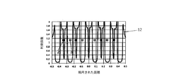
図6は、図1の対応するセンサ構造の感知素子ストリング2および基準素子ストリング3の位置と、対応する位置における利得係数との間の関係曲線である。比較を容易にするために、基準素子ストリング3および感知素子ストリング2の数は、図5における基準素子ストリング3および感知素子ストリング2の数と同じである。図5および図6の2つの曲線12および13を比較することによって、本発明においては感知素子ストリング2の位置における磁場の大きさが、大きく減衰させられており、したがってたとえ本発明のシングルチップ基準ブリッジ式磁場センサが高強度の磁場に配置されたとしても、センサによって感知される磁場は減衰させられた磁場であり、それがセンサの飽和範囲の範囲内である限りにおいて、センサが依然として正常に機能できることを、見て取ることができる。
FIG. 6 is a relationship curve between the position of the
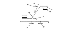
図7は、TMRおよびGMRスピンバルブ構造の磁気抵抗感知素子の応答曲線である。外部から印加される磁場11の方向がピン層の磁化方向19に平行であり、外部から印加される磁場の強度が−Bs+Bo 25よりも大きい場合、磁気フリー層の磁化方向18は、外部から印加される磁場11の方向に平行であり、さらにピン層の磁化方向19に平行であり、この瞬間において、TMR素子の磁気抵抗は最小であり、すなわちRL 21である。外部から印加される磁場11の方向がピン層の磁化方向19に逆平行であり、外部から印加される磁場の強度がBs+Bo 26よりも大きい場合、磁気フリー層の磁化方向18は、外部から印加される磁場11の方向に平行であり、さらにピン層の磁化方向19に逆平行であり、この瞬間において、TMR素子の磁気抵抗は最大であり、すなわちRH 22である。外部から印加される磁場11の強度がBo 23である場合、磁気フリー層の磁化方向18は、ピン層の磁化方向19に垂直であり、この瞬間において、TMR素子の磁気抵抗はRL 21およびRH 22の中央の値であり、すなわち(RL+RH)/2である。−Bs+Bo 25とBs+Bo 26との間の磁場が、シングルチップ線形ブリッジ式磁場センサの測定範囲である。この図から、曲線20が−Bs+Bo 25とBs+Bo 26との間において線形であり、抵抗変化率が(RH−RL)/RL×100%=ΔR/RL×100%であることを、見て取ることができる。
FIG. 7 is a response curve of magnetoresistive sensing elements of TMR and GMR spin valve structure. When the direction of the externally applied
TMRスピンバルブについて、その抵抗変化率が最大で200%になり得る一方で、GMRスピンバルブについては、その抵抗変化率は最大で10%にすぎない。 For TMR spin valves, the rate of change of resistance can be up to 200%, while for GMR spin valves, the rate of change of resistance is only up to 10%.
図8は、TMR3層膜構造およびGMR多層膜構造の磁気抵抗感知素子の応答曲線である。外部から印加される磁場11の方向がピン層の磁化方向19に平行であり、外部から印加される磁場の強度が−Bs 31またはBs 32よりも大きい場合、磁気フリー層の磁化方向18は、外部から印加される磁場11の方向に平行であり、さらにピン層の磁化方向19に平行であり、この瞬間において、MTJ素子の磁気抵抗は最小であり、すなわちRL 28である。外部から印加される磁場が0である場合、磁気フリー層の磁化方向18は、ピン層の磁化方向19に逆平行であり、この瞬間において、MTJ素子の磁気抵抗は最大であり、すなわちRH 27である。−Bs 31とBs 32との間の磁場が、センサの測定範囲である。この図から、曲線29および30が、−Bs 31とBs 32との間において線形であり、磁気抵抗素子の抵抗変化率が、やはり最大で200%になり得ることを、見て取ることができる。
FIG. 8 is a response curve of a magnetoresistive sensing element having a TMR three-layer film structure and a GMR multilayer film structure. If the direction of the externally applied
図9は、AMR Barber−pole構造の磁気抵抗感知素子の応答曲線である。この図から、磁気抵抗素子の抵抗変化率が約1%であることを、見て取ることができる。 FIG. 9 is a response curve of the magnetoresistive sensing element of the AMR Barber-pole structure. From this figure, it can be seen that the rate of change in resistance of the magnetoresistive element is about 1%.
図10は、TMRスピンバルブ構造の磁気抵抗感知素子を備えるシングルチップ基準ブリッジ式センサについて、減衰器がある場合および減衰器がない場合の変換特性曲線である。曲線15が、減衰器が存在しない状況を示し、曲線16が、減衰器が使用されている状況を示しており、横軸は、外部から印加される磁場の大きさを表し、縦軸は、電源電圧に対するセンサ出力電圧の比を表している。2つの曲線を比較することによって、曲線15に対応する磁場の線形性の範囲が約35[Oe]である一方で、曲線16に対応する磁場の線形性の範囲が約150[Oe]であり、したがってセンサの線形な動作範囲が、減衰器の使用後に明らかに広くなっていることを、見て取ることができる。
FIG. 10 is a conversion characteristic curve with and without an attenuator for a single chip reference bridge type sensor having a magnetoresistive sensing element of TMR spin valve structure.
図11は、TMR3層膜構造の磁気抵抗感知素子を備えるシングルチップ基準ブリッジ式センサについて、減衰器がある場合および減衰器がない場合の変換特性曲線である。曲線33が、減衰器が存在しない状況を示し、曲線34が、減衰器が使用されている状況を示しており、横軸は、外部から印加される磁場の大きさを表し、縦軸は、電源電圧に対するセンサ出力電圧の比を表している。2つの曲線を比較することによって、センサの動作範囲が、減衰器の使用後に明らかに広くなっていることを、見て取ることができる。
FIG. 11 is a conversion characteristic curve with and without an attenuator for a single-chip reference bridge type sensor including a magnetoresistive sensing element having a TMR three-layer film structure.
上述の内容は、ブリッジがフルブリッジである状況である。ハーフブリッジおよび疑似ブリッジの動作原理は、フルブリッジの動作原理と同じであるため、ここでは動作原理を繰り返し説明することはしない。上記にて得られた結論は、ハーフブリッジおよび疑似ブリッジ構造のシングルチップ基準ブリッジ式磁場センサにも適用可能である。 The above is the situation where the bridge is a full bridge. The operating principle of the half bridge and the pseudo bridge is the same as the operating principle of the full bridge, so the operating principle will not be described repeatedly here. The conclusions obtained above are also applicable to single-chip reference bridge type magnetic field sensors of half bridge and pseudo bridge structure.
上述の実施形態は、本発明の好ましい実施形態にすぎず、本発明を限定するために使用されるものではない。当業者にとって、本発明は、種々の変更および変形を有することができる。本発明の精神および原理の範囲内で行われるあらゆる修正、同等物による置き換え、改善なども、本発明の保護の範囲に含まれなければならない。
The embodiments described above are only preferred embodiments of the present invention and are not used to limit the present invention. For those skilled in the art, the present invention may have various modifications and variations. All modifications, equivalent replacements, improvements and the like made within the spirit and principle of the present invention should be included in the protection scope of the present invention.
Claims (16)
基板と、
前記基板上に配置され、1つまたは少なくとも2つの同一な電気的に相互接続された磁気抵抗感知素子を備える少なくとも1つの行または列の基準素子ストリングを備えている少なくとも1つの基準アームと、
前記基板上に配置され、1つまたは少なくとも2つの同一な電気的に相互接続された磁気抵抗感知素子を備える少なくとも1つの行または列の感知素子ストリングを備えている少なくとも1つの感知アームと、
少なくとも1つの減衰器および少なくとも2つの遮へい構造と、を備えており、
前記減衰器および前記遮へい構造は、間隔を空けて互いに交互に配置され、前記減衰器および前記遮へい構造の形状は、同じであり、前記遮へい構造の幅および面積は、それぞれ前記減衰器の幅および面積よりも大きく、
前記基準アームおよび前記感知アームは、ブリッジを形成するように接続され、
各々の基準素子ストリングは、自身の上に遮へい構造を有するように設計され、各々の感知素子ストリングは、自身の上に減衰器を有するように設計され、前記基準素子ストリングは、前記遮へい構造の下方または上方に位置し、前記感知素子ストリングは、前記減衰器の下方または上方に位置し、
前記基準素子ストリングおよび前記感知素子ストリングは、行または列の数において同じであり、行方向または列方向に沿って間隔を空けて互いに交互に配置され、
前記感知素子ストリングの位置における磁場の利得係数が、前記基準素子ストリングの位置における磁場の利得係数よりも大きい、ことを特徴とするシングルチップ基準ブリッジ式磁場センサ。 A single chip reference bridge type magnetic field sensor,
A substrate,
At least one reference arm comprising a reference element string of at least one row or column disposed on the substrate and comprising one or at least two identical electrically interconnected magnetoresistive sensing elements;
At least one sensing arm comprising at least one row or column of sensing element strings disposed on the substrate and comprising one or at least two identical electrically interconnected magnetoresistive sensing elements;
At least one attenuator and at least two shielding structures;
The attenuators and the shielding structures are alternately spaced apart from each other, the shape of the attenuators and the shielding structures being the same, and the width and area of the shielding structures are respectively the width of the attenuators and the shielding structures. Greater than area,
The reference arm and the sensing arm are connected to form a bridge,
Each reference element string is designed to have a shielding structure on itself and each sensing element string is designed to have an attenuator on itself, said reference element string being of said shielding structure Located below or above, the sensing element string is located below or above the attenuator,
The reference element string and the sensing element string are the same in the number of rows or columns, and are alternately arranged mutually spaced apart along the row or column direction ,
A single chip reference bridge type magnetic field sensor characterized in that the gain factor of the magnetic field at the position of the sensing element string is larger than the gain factor of the magnetic field at the position of the reference element string .
Applications Claiming Priority (3)
| Application Number | Priority Date | Filing Date | Title |
|---|---|---|---|
| CN201310719255.9 | 2013-12-24 | ||
| CN201310719255.9A CN103645449B (en) | 2013-12-24 | 2013-12-24 | A kind of single-chip for high-intensity magnetic field refers to bridge type magnetic sensor |
| PCT/CN2014/094838 WO2015096744A1 (en) | 2013-12-24 | 2014-12-24 | Single chip reference bridge type magnetic sensor for high-intensity magnetic field |
Publications (3)
| Publication Number | Publication Date |
|---|---|
| JP2017502298A JP2017502298A (en) | 2017-01-19 |
| JP2017502298A5 JP2017502298A5 (en) | 2018-12-06 |
| JP6509231B2 true JP6509231B2 (en) | 2019-05-08 |
Family
ID=50250699
Family Applications (1)
| Application Number | Title | Priority Date | Filing Date |
|---|---|---|---|
| JP2016542947A Active JP6509231B2 (en) | 2013-12-24 | 2014-12-24 | Single-chip reference bridge magnetic sensor for high magnetic fields |
Country Status (5)
| Country | Link |
|---|---|
| US (1) | US10024930B2 (en) |
| EP (1) | EP3088908B1 (en) |
| JP (1) | JP6509231B2 (en) |
| CN (1) | CN103645449B (en) |
| WO (1) | WO2015096744A1 (en) |
Families Citing this family (14)
| Publication number | Priority date | Publication date | Assignee | Title |
|---|---|---|---|---|
| CN103645449B (en) * | 2013-12-24 | 2015-11-25 | 江苏多维科技有限公司 | A kind of single-chip for high-intensity magnetic field refers to bridge type magnetic sensor |
| CN103954920B (en) * | 2014-04-17 | 2016-09-14 | 江苏多维科技有限公司 | A kind of single-chip tri-axis linear magnetic sensor and preparation method thereof |
| CN104301851B (en) | 2014-07-14 | 2018-01-26 | 江苏多维科技有限公司 | TMR near fields magnetic communication system |
| CN104280700B (en) * | 2014-09-28 | 2017-09-08 | 江苏多维科技有限公司 | A kind of single-chip difference free layer push-pull type magnetic field sensor electric bridge and preparation method |
| CN104698409B (en) | 2015-02-04 | 2017-11-10 | 江苏多维科技有限公司 | A kind of single-chip has the high-intensity magnetic field X-axis linear magnetoresistance sensor of alignment coil/replacement coil |
| CN104776794B (en) * | 2015-04-16 | 2017-11-10 | 江苏多维科技有限公司 | A kind of high-intensity magnetic field magneto-resistor angular transducer singly encapsulated |
| CN105259518A (en) | 2015-11-03 | 2016-01-20 | 江苏多维科技有限公司 | High-sensitivity single-chip push-pull type TMR magnetic field sensor |
| CN108072850B (en) | 2016-11-09 | 2020-06-12 | 爱盛科技股份有限公司 | Magnetic field sensing device |
| CN107037382B (en) | 2017-04-05 | 2023-05-30 | 江苏多维科技有限公司 | Pre-modulation magneto-resistance sensor |
| JP6996478B2 (en) | 2018-11-16 | 2022-02-04 | Tdk株式会社 | Magnetic sensor and position detector |
| JP7006670B2 (en) | 2019-10-24 | 2022-01-24 | Tdk株式会社 | Magnetic sensor |
| US20220326321A1 (en) | 2021-04-12 | 2022-10-13 | Jochen Schmitt | Magnetic field sensor with overcurrent detection |
| CN115236568B (en) * | 2022-09-23 | 2023-01-20 | 南方电网数字电网研究院有限公司 | Wide-range vertical sensitive magnetic sensor based on magnetic flux regulator and preparation method thereof |
| CN115963437B (en) * | 2022-12-21 | 2023-10-20 | 南方电网数字电网研究院有限公司 | Multi-range magnetic sensor, magnetic field measuring method and conductor preparation method |
Family Cites Families (25)
| Publication number | Priority date | Publication date | Assignee | Title |
|---|---|---|---|---|
| US3887944A (en) * | 1973-06-29 | 1975-06-03 | Ibm | Method for eliminating part of magnetic crosstalk in magnetoresistive sensors |
| JP2663460B2 (en) * | 1987-10-09 | 1997-10-15 | 株式会社デンソー | Magnetic direction sensor |
| US5217010A (en) * | 1991-05-28 | 1993-06-08 | The Johns Hopkins University | Ecg amplifier and cardiac pacemaker for use during magnetic resonance imaging |
| US6185078B1 (en) * | 1998-08-21 | 2001-02-06 | International Business Machines Corporation | Spin valve read head with antiferromagnetic oxide film as longitudinal bias layer and portion of first read gap |
| US6771472B1 (en) * | 2001-12-07 | 2004-08-03 | Seagate Technology Llc | Structure to achieve thermally stable high sensitivity and linear range in bridge GMR sensor using SAF magnetic alignments |
| JP4977378B2 (en) * | 2006-02-23 | 2012-07-18 | 山梨日本電気株式会社 | Magnetic sensor, rotation detection device, and position detection device |
| JP4805344B2 (en) * | 2006-04-13 | 2011-11-02 | 旭化成エレクトロニクス株式会社 | Magnetic sensor and manufacturing method thereof |
| US7639005B2 (en) * | 2007-06-15 | 2009-12-29 | Advanced Microsensors, Inc. | Giant magnetoresistive resistor and sensor apparatus and method |
| US7795862B2 (en) * | 2007-10-22 | 2010-09-14 | Allegro Microsystems, Inc. | Matching of GMR sensors in a bridge |
| JP5500785B2 (en) | 2008-05-14 | 2014-05-21 | 新科實業有限公司 | Magnetic sensor |
| JP5250109B2 (en) * | 2009-06-12 | 2013-07-31 | アルプス・グリーンデバイス株式会社 | Magnetic balanced current sensor |
| CN102298125B (en) * | 2011-03-03 | 2013-01-23 | 江苏多维科技有限公司 | Push-pull bridge magneto resistor sensor |
| WO2012120940A1 (en) * | 2011-03-07 | 2012-09-13 | アルプス電気株式会社 | Current sensor |
| CN102621504B (en) * | 2011-04-21 | 2013-09-04 | 江苏多维科技有限公司 | Monolithic reference full bridge magnetic field sensor |
| CN102323554A (en) | 2011-05-17 | 2012-01-18 | 杭州电子科技大学 | Integrated coil-biased giant magnetoresistance magneto-dependent sensor |
| JP2013053903A (en) * | 2011-09-02 | 2013-03-21 | Alps Green Devices Co Ltd | Current sensor |
| CN102565727B (en) * | 2012-02-20 | 2016-01-20 | 江苏多维科技有限公司 | For measuring the magnetic resistance sensor in magnetic field |
| JP2013210335A (en) * | 2012-03-30 | 2013-10-10 | Alps Electric Co Ltd | Magnetic sensor |
| CN203337808U (en) * | 2013-05-28 | 2013-12-11 | 江苏多维科技有限公司 | Single-chip bridge-type magnetic field sensor |
| CN103267955B (en) * | 2013-05-28 | 2016-07-27 | 江苏多维科技有限公司 | Single-chip bridge-type magnetic field sensor |
| CN203587786U (en) * | 2013-10-21 | 2014-05-07 | 江苏多维科技有限公司 | Push-pull bridge type magnetic sensor for high-intensity magnetic field |
| CN103592608B (en) * | 2013-10-21 | 2015-12-23 | 江苏多维科技有限公司 | A kind of push-pull bridge type magnetic sensor for high-intensity magnetic field |
| CN103630855B (en) * | 2013-12-24 | 2016-04-13 | 江苏多维科技有限公司 | A kind of High-sensitivity push-pull bridge type magnetic sensor |
| CN103645449B (en) | 2013-12-24 | 2015-11-25 | 江苏多维科技有限公司 | A kind of single-chip for high-intensity magnetic field refers to bridge type magnetic sensor |
| CN203658561U (en) * | 2013-12-24 | 2014-06-18 | 江苏多维科技有限公司 | Single-chip reference bridge type magnetic sensor for high-intensity magnetic field |
-
2013
- 2013-12-24 CN CN201310719255.9A patent/CN103645449B/en active Active
-
2014
- 2014-12-24 EP EP14874846.0A patent/EP3088908B1/en active Active
- 2014-12-24 JP JP2016542947A patent/JP6509231B2/en active Active
- 2014-12-24 WO PCT/CN2014/094838 patent/WO2015096744A1/en active Application Filing
- 2014-12-24 US US15/108,162 patent/US10024930B2/en active Active
Also Published As
| Publication number | Publication date |
|---|---|
| EP3088908B1 (en) | 2021-10-20 |
| JP2017502298A (en) | 2017-01-19 |
| EP3088908A1 (en) | 2016-11-02 |
| CN103645449B (en) | 2015-11-25 |
| CN103645449A (en) | 2014-03-19 |
| EP3088908A4 (en) | 2017-09-20 |
| US10024930B2 (en) | 2018-07-17 |
| US20160327616A1 (en) | 2016-11-10 |
| WO2015096744A1 (en) | 2015-07-02 |
Similar Documents
| Publication | Publication Date | Title |
|---|---|---|
| JP6509231B2 (en) | Single-chip reference bridge magnetic sensor for high magnetic fields | |
| JP2017502298A5 (en) | ||
| JP6474822B2 (en) | High sensitivity push-pull bridge magnetic sensor | |
| JP6461946B2 (en) | Push-pull bridge type magnetic sensor for high intensity magnetic field | |
| JP6525335B2 (en) | Single chip bridge type magnetic field sensor | |
| JP6193212B2 (en) | Single chip 2-axis bridge type magnetic field sensor | |
| JP6420665B2 (en) | Magnetoresistive sensor for measuring magnetic fields | |
| US9465056B2 (en) | Current sensor with temperature-compensated magnetic tunnel junction bridge | |
| US9678178B2 (en) | Magnetoresistive magnetic field gradient sensor | |
| CN202421483U (en) | Single-chip push-pull bridge-type magnetic field sensor | |
| JP2014512003A (en) | Single-chip push-pull bridge type magnetic field sensor | |
| JP2014517264A (en) | Single-chip reference full-bridge magnetic field sensor | |
| CN203658561U (en) | Single-chip reference bridge type magnetic sensor for high-intensity magnetic field | |
| CN203337808U (en) | Single-chip bridge-type magnetic field sensor | |
| CN202210145U (en) | MTJ triaxial magnetic field sensor |
Legal Events
| Date | Code | Title | Description |
|---|---|---|---|
| A621 | Written request for application examination |
Free format text: JAPANESE INTERMEDIATE CODE: A621 Effective date: 20170911 |
|
| A977 | Report on retrieval |
Free format text: JAPANESE INTERMEDIATE CODE: A971007 Effective date: 20180629 |
|
| A131 | Notification of reasons for refusal |
Free format text: JAPANESE INTERMEDIATE CODE: A131 Effective date: 20180801 |
|
| A524 | Written submission of copy of amendment under article 19 pct |
Free format text: JAPANESE INTERMEDIATE CODE: A524 Effective date: 20181029 |
|
| TRDD | Decision of grant or rejection written | ||
| A01 | Written decision to grant a patent or to grant a registration (utility model) |
Free format text: JAPANESE INTERMEDIATE CODE: A01 Effective date: 20190329 |
|
| A61 | First payment of annual fees (during grant procedure) |
Free format text: JAPANESE INTERMEDIATE CODE: A61 Effective date: 20190402 |
|
| R150 | Certificate of patent or registration of utility model |
Ref document number: 6509231 Country of ref document: JP Free format text: JAPANESE INTERMEDIATE CODE: R150 |
|
| R250 | Receipt of annual fees |
Free format text: JAPANESE INTERMEDIATE CODE: R250 |
|
| R250 | Receipt of annual fees |
Free format text: JAPANESE INTERMEDIATE CODE: R250 |
|
| R250 | Receipt of annual fees |
Free format text: JAPANESE INTERMEDIATE CODE: R250 |