EP2826139B1 - Stromregelung für gleichspannungswandler - Google Patents
Stromregelung für gleichspannungswandler Download PDFInfo
- Publication number
- EP2826139B1 EP2826139B1 EP13709207.8A EP13709207A EP2826139B1 EP 2826139 B1 EP2826139 B1 EP 2826139B1 EP 13709207 A EP13709207 A EP 13709207A EP 2826139 B1 EP2826139 B1 EP 2826139B1
- Authority
- EP
- European Patent Office
- Prior art keywords
- primary
- voltage
- switching
- phase
- bridges
- Prior art date
- Legal status (The legal status is an assumption and is not a legal conclusion. Google has not performed a legal analysis and makes no representation as to the accuracy of the status listed.)
- Not-in-force
Links
Images


Classifications
-
- H—ELECTRICITY
- H02—GENERATION; CONVERSION OR DISTRIBUTION OF ELECTRIC POWER
- H02M—APPARATUS FOR CONVERSION BETWEEN AC AND AC, BETWEEN AC AND DC, OR BETWEEN DC AND DC, AND FOR USE WITH MAINS OR SIMILAR POWER SUPPLY SYSTEMS; CONVERSION OF DC OR AC INPUT POWER INTO SURGE OUTPUT POWER; CONTROL OR REGULATION THEREOF
- H02M3/00—Conversion of dc power input into dc power output
- H02M3/22—Conversion of dc power input into dc power output with intermediate conversion into ac
- H02M3/24—Conversion of dc power input into dc power output with intermediate conversion into ac by static converters
- H02M3/28—Conversion of dc power input into dc power output with intermediate conversion into ac by static converters using discharge tubes with control electrode or semiconductor devices with control electrode to produce the intermediate ac
- H02M3/325—Conversion of dc power input into dc power output with intermediate conversion into ac by static converters using discharge tubes with control electrode or semiconductor devices with control electrode to produce the intermediate ac using devices of a triode or a transistor type requiring continuous application of a control signal
- H02M3/335—Conversion of dc power input into dc power output with intermediate conversion into ac by static converters using discharge tubes with control electrode or semiconductor devices with control electrode to produce the intermediate ac using devices of a triode or a transistor type requiring continuous application of a control signal using semiconductor devices only
- H02M3/33507—Conversion of dc power input into dc power output with intermediate conversion into ac by static converters using discharge tubes with control electrode or semiconductor devices with control electrode to produce the intermediate ac using devices of a triode or a transistor type requiring continuous application of a control signal using semiconductor devices only with automatic control of the output voltage or current, e.g. flyback converters
-
- H—ELECTRICITY
- H02—GENERATION; CONVERSION OR DISTRIBUTION OF ELECTRIC POWER
- H02M—APPARATUS FOR CONVERSION BETWEEN AC AND AC, BETWEEN AC AND DC, OR BETWEEN DC AND DC, AND FOR USE WITH MAINS OR SIMILAR POWER SUPPLY SYSTEMS; CONVERSION OF DC OR AC INPUT POWER INTO SURGE OUTPUT POWER; CONTROL OR REGULATION THEREOF
- H02M3/00—Conversion of dc power input into dc power output
- H02M3/22—Conversion of dc power input into dc power output with intermediate conversion into ac
- H02M3/24—Conversion of dc power input into dc power output with intermediate conversion into ac by static converters
- H02M3/28—Conversion of dc power input into dc power output with intermediate conversion into ac by static converters using discharge tubes with control electrode or semiconductor devices with control electrode to produce the intermediate ac
- H02M3/325—Conversion of dc power input into dc power output with intermediate conversion into ac by static converters using discharge tubes with control electrode or semiconductor devices with control electrode to produce the intermediate ac using devices of a triode or a transistor type requiring continuous application of a control signal
- H02M3/335—Conversion of dc power input into dc power output with intermediate conversion into ac by static converters using discharge tubes with control electrode or semiconductor devices with control electrode to produce the intermediate ac using devices of a triode or a transistor type requiring continuous application of a control signal using semiconductor devices only
- H02M3/33569—Conversion of dc power input into dc power output with intermediate conversion into ac by static converters using discharge tubes with control electrode or semiconductor devices with control electrode to produce the intermediate ac using devices of a triode or a transistor type requiring continuous application of a control signal using semiconductor devices only having several active switching elements
- H02M3/33576—Conversion of dc power input into dc power output with intermediate conversion into ac by static converters using discharge tubes with control electrode or semiconductor devices with control electrode to produce the intermediate ac using devices of a triode or a transistor type requiring continuous application of a control signal using semiconductor devices only having several active switching elements having at least one active switching element at the secondary side of an isolation transformer
- H02M3/33584—Bidirectional converters
-
- H—ELECTRICITY
- H02—GENERATION; CONVERSION OR DISTRIBUTION OF ELECTRIC POWER
- H02M—APPARATUS FOR CONVERSION BETWEEN AC AND AC, BETWEEN AC AND DC, OR BETWEEN DC AND DC, AND FOR USE WITH MAINS OR SIMILAR POWER SUPPLY SYSTEMS; CONVERSION OF DC OR AC INPUT POWER INTO SURGE OUTPUT POWER; CONTROL OR REGULATION THEREOF
- H02M1/00—Details of apparatus for conversion
- H02M1/14—Arrangements for reducing ripples from dc input or output
-
- H—ELECTRICITY
- H02—GENERATION; CONVERSION OR DISTRIBUTION OF ELECTRIC POWER
- H02M—APPARATUS FOR CONVERSION BETWEEN AC AND AC, BETWEEN AC AND DC, OR BETWEEN DC AND DC, AND FOR USE WITH MAINS OR SIMILAR POWER SUPPLY SYSTEMS; CONVERSION OF DC OR AC INPUT POWER INTO SURGE OUTPUT POWER; CONTROL OR REGULATION THEREOF
- H02M1/00—Details of apparatus for conversion
- H02M1/44—Circuits or arrangements for compensating for electromagnetic interference in converters or inverters
Definitions
- the invention relates to DC-DC converters with a so-called dual-active-bridge (DAB) topology and a method for operating these DC-DC converters.
- DAB dual-active-bridge
- a DC-DC converter also referred to as a DC-DC converter, denotes an electrical circuit which converts a DC voltage supplied to the input into a DC voltage with a higher, lower or inverted voltage level.
- DC-DC converters are used, for example, in switching power supplies of PC power supplies, notebooks, mobile telephones, small motors, hi-fi equipment. The advantages over linear power supplies are better efficiency and lower heat generation. For a linear voltage regulator or a series resistor, however, the superfluous voltage is simply "burned".
- DC-DC converters are also available as fully encapsulated converter modules, some of which are intended for direct placement on printed circuit boards. Depending on the design, the output voltage (secondary voltage) may be smaller, equal to or greater than the input voltage (primary voltage). Best known are the modules, which translate a low voltage to a galvanically isolated low voltage.
- the encapsulated DC-DC converters are offered, for example, for insulation voltages of 1.5 kV to over 3 kV and are used to power small consumers in DC networks such as 24 V in industrial plants or 48 V in telecommunications or in the field of electronic assemblies, for example 5 Volts for digital circuits or ⁇ 15 volts for the operation of operational amplifiers.
- DC-DC converters are classified according to various criteria and divided into different topologies (type of construction of a branched network of electricity routes) divided. In contrast to unidirectional converters, with bi-directional DC-DC converters, it is irrelevant which port is defined as the input and which port is defined as the output. A bidirectional energy flow direction allows both a power flow from the defined input (primary side) to the output (secondary side) and vice versa.
- DC-DC converters based on the principle of a "dual active bridge (DAB)" topology
- DAB dual active bridge
- the DC input voltage in an input converter is converted to an AC voltage and fed to a transformer.
- the output of the transformer is connected to an output transducer, which converts the AC voltage back to a DC output voltage for a load.
- These DC / DC converters can be implemented in single-phase or multi-phase configurations.
- Such DAB DC / DC converter topologies such as in document US 5027264 are high efficiency transducer topologies that allow bi-directional power flow, isolation across the transformer, and high voltage operation. This type of converter is particularly suitable for use in medium-voltage DC networks.
- the transmitted power is adjusted by varying the phase angle between the voltage on the primary side and the voltage on the secondary side. If the transmitted power is changed abruptly, undesired oscillations and an asymmetrical distribution of the currents in the phases occur.
- the oscillation decays with the time constant L / R, where L denotes the sum of the leakage inductance of the primary winding and the primary side leakage inductance of the secondary winding of the transformer, and R is the sum of the resistance of the primary winding and the primary-side related resistance of the secondary winding. It would therefore be desirable for the oscillations to decay quickly in time, which would require a small time constant L / R.
- This object is achieved by a method for operating an at least three-phase DC-DC converter having a primary side comprising at least three actively connected primary-side voltage bridges with a plurality of active switches for converting a DC input voltage into primary-side AC voltages for each of the primary-side voltage bridges and a secondary side comprising at least three actively connected secondary-side Voltage bridges with a plurality of active switches for converting the secondary side AC voltages for each of the secondary side voltage bridges into a common DC output voltage, wherein each of the primary side voltage bridges is coupled to one of the secondary side voltage bridges via a polyphase transformer or via a respective transformer to a respective phase, wherein the primary and secondary AC voltages having a period T shifted by a phase angle ⁇ , comprising the steps of adjusting the phase angle ⁇ from a first phase angle ⁇ 1 to a second phase angle ⁇ 2 as a switching operation for transmitting power from the primary to the secondary side, wherein the primary and secondary-side voltage bridges in the switching operation are switched so that the
- a DAB DC / DC converter which enables a rapid change in the phase angle while minimizing or avoiding the oscillations in the DC current during power changes. Without minimizing or avoiding the oscillations in the DC current, the phase angle could only be changed slowly.
- the present invention enables a rapid change of the phase angle, which allows a highly dynamic adjustment of the DC current (rapid regulation of the current) and thus a fast power transmission.
- the method according to the invention makes possible a highly dynamic change in the transmitted power in contrast to the prior art, where DAB DC / DC converters are used in stationary operation.
- the phase angle ⁇ of the various phases is set independently of falling and rising edges of the primary-side and secondary-side alternating voltages.
- the DC-DC converter according to the invention are particularly suitable as a DC / DC converter for medium to high power and so-called pulsed power applications with high demands on the dynamics.
- the primary side indicates that part of the DC / DC converter that faces the energetic energy source.
- the secondary side indicates the other side of the transformer connected to the electrical load.
- the primary and secondary sides are isolated from each other by the transformer. If the DAB DC / DC converter is bidirectional, then For example, the primary side in a bidirectional DC-DC converter may represent the secondary side in another bidirectional DC-DC converter.
- the DC-DC converter according to the present invention can be designed as a three- or multi-phase DAB DC / DC converter, for example, as a five-phase DAB DC / DC converter.
- the DC input voltage is applied to the voltage bridges with the active switches and is converted in the voltage bridges by the circuit of the active switch (switching operation) in an AC voltage. Since the switches are usually switched on completely, the output bridges produce approximately rectangular alternating voltages (square-wave voltage). The voltage across the transformer windings thereby becomes step-shaped. Optionally, the edges of the square wave voltage are not infinitely steep due to the use of so-called snubbers, d. H. the shape deviates from the square-wave voltage (step shape at the transformer windings). Snubbers are used to ensure dynamic voltage balance during switching operations (snubber network).
- a snubber network is an electrical circuit with snubber links, e.g. annoying high frequencies or voltage spikes, which usually occur when switching inductive loads, to neutralize in an abrupt interruption of the current flow. Snubber links limit the voltage slew rate or current slew rate on semiconductors.
- Suitable switches for the voltage bridges are active semiconductor switches (power semiconductors), such as turn-off thyristors, transistors, MOSFETs, IGBTs (Insulated Gate Bipolar Transistors) or IGCTs (Integrated Gate-Commutated Thyristor) with intelligent gate drivers.
- active semiconductor switches power semiconductors
- IGBTs Insulated Gate Bipolar Transistors
- IGCTs Integrated Gate-Commutated Thyristor
- the transformer here refers to the magnetic circuit - usually a ferrite or Iron core -, with the corresponding windings of the primary and secondary voltage bridges around the magnetic core around. If each of the phases comprises a separate transformer, only the conductors of a primary-side phase and the corresponding other secondary-side phase are wound around the transformer associated with this phase. The magnetic cores of the individual phase transformers are then physically separated.
- a polyphase transformer refers to a transformer having a common magnetic core for all phases, the windings of the primary and secondary voltage bridges of the individual phases being arranged at different regions of the magnetic core.
- the polyphase transformer is a three-phase transformer.
- the principle of a DAB DC-DC converter is to cause in both cases via the AC voltages at the transformer a targeted voltage drop across the leakage inductance of the transformer and thus to control the power flow.
- Actively connected voltage bridges allow the independent control of the displacement angle (phase angle) between the primary and secondary alternating voltages applied to the transformer and thus the targeted control of the power flow.
- the phase angle ⁇ designates the displacement of the primary side and secondary side alternating voltages, each with the period T against each other.
- the first phase angle ⁇ 1 denotes the displacement of the primary-side and secondary-side alternating voltages relative to one another before the beginning of a switching operation.
- the second phase angle ⁇ 2 denotes the displacement of the primary-side and secondary-side alternating voltages relative to each other after completion of the switching operation.
- the phase angles ⁇ may also take one or more values between ⁇ 1 and ⁇ 2, where ⁇ 1 may be larger or smaller than ⁇ 2.
- the phase angle ⁇ can assume positive and negative values.
- a positive value ⁇ between a first and a second alternating voltage means that the second alternating voltage lags the first alternating voltage in the course of the alternating voltages.
- a negative value ⁇ between a first and a second AC voltage means that the second AC voltage leads (or leads) the first AC voltage in the course of the alternating voltages.
- phase angles ⁇ of the individual phases for the balancing of the currents in the phases are set differently.
- the method is not limited to using equal phase angles for all phases.
- asymmetries of the transformers for example, can be balanced so that there is nevertheless a symmetrical current distribution in the phases.
- the DC-DC converter is a three-phase DC-DC converter with three actively connected primary-side voltage bridges, each having two or more active switches and three actively connected secondary-side voltage bridges each having two or more active switches, wherein during the switching operation, the setting of the phase angle ⁇ 2 for all three phases at the same edges (ie either only at the rising edges of the AC voltages of the phases or only on the falling edges of the AC voltages of the phases) of the primary and secondary AC voltage at the primary and secondary voltage bridges takes place.
- a three-phase DC-DC converter with DAB topology has the advantage of significantly increasing the available power density through the improved use of the available apparent power of the transformer.
- the number of switches may in one embodiment consist of two switches per voltage bridge.
- the DC-DC converter according to the present invention is a three-phase DAB NPC DC / DC converter.
- NPC stands for "neutral-point-clamped".
- the levels of the voltages can be set symmetrically in the three-phase DAB NPC DC / DC converter via clamping diodes, so that the medium voltage corresponds to the voltage zero level without that Symmetrization networks and / or drivers would be required.
- IGBTs insulated gate bipolar transistors
- ANPC inverters may be used or capacitances used in so-called FLCs for voltage sharing.
- the method is applicable to phase shifts of 120 ° between the voltages of the first, second and third primary-side voltage bridges or the first, second and third secondary-side voltage bridges, however, the method is not limited to phase shifts of 120 °. Also, the method is not limited to the above order of the circuits of the individual bridges. The method can also be applied to cyclic switching of the circuits or reversal of the circuits.
- primary-side / secondary-side or "secondary-side / primary-side” designate the corresponding circuits either for the pages before or else for the pages after the slash "/".
- the former sides correspond to the circuits for current flow in the one direction
- the sides following the slash correspond to the circuits for the reverse current flow.
- a fast power flow reversal and a symmetrical current distribution in the three phases are possible. If the primary and secondary alternating voltages are shifted by a positive phase angle, the secondary-side alternating voltage switches in a lagging manner to the primary-side alternating voltage. If, on the other hand, the primary and secondary alternating voltages are shifted by a negative phase angle, then the secondary-side alternating voltage switches in advance (or leading) to the primary-side alternating voltage. Both of these possibilities are from the above procedure includes.
- phase currents are also avoided in addition.
- the setpoint current is already reached after T / 2.
- This method is characterized by the fact that no oscillations are excited and that not too short time after the change of the phase angle, an increased phase current occurs.
- This method thus achieves the desired current later (T / 2 instead of T / 3) compared to the above alternative method, but without a briefly slightly increased phase current, even when sign changes the phase angle.
- the method is applicable to phase shifts of 120 ° between the voltages of the first, second and third primary-side voltage bridges and the first, second and third secondary-side voltage bridges, however, the method is also not limited to phase shifts of 120 °.
- the method is not limited to the above order of the circuits of the individual bridges.
- the method can also be applied to cyclic switching of the circuits or reversal of the circuits.
- the terms "primary-side / secondary-side” or “secondary-side / primary-side” designate the corresponding circuits either for the pages before or else for the pages after the slash "/".
- the former pages before the Slash
- the circuits for a current flow in the one direction and the sides following the slash correspond to the circuits for the reverse current flow.
- the secondary-side alternating voltage switches in a lagging manner to the primary-side alternating voltage. If, on the other hand, the primary and secondary alternating voltages are shifted by a negative phase angle, then the secondary-side alternating voltage switches in advance (or leading) to the primary-side alternating voltage. Both of these possibilities are encompassed by the above method.
- the switching operation for setting the second phase angle ⁇ 2 comprises one or more periods T of the primary-side and secondary-side alternating voltages, and the phase angle ⁇ between the primary-side and secondary-side alternating voltages is set step by step in several steps to the second phase angle ⁇ 2 at the edge.
- the stepwise adjustment of the phase angle ⁇ 2 takes place linearly in equal steps. As a result, possible slightly increased phase currents can be better suppressed. This method is advantageous if the current is to be changed linearly within a time period greater than T / 2.
- phase angles ⁇ of the rising and falling edges in the switching operation are adapted starting from the above phase angles for the compensation of transformer and switch influences.
- influences can be compensated that can not be avoided by the topology alone.
- the DC-DC converter is operated such that the phase shifts between the primary-side AC voltages of the primary-side voltage bridges with each other and the Phase deviations between the secondary-side alternating voltages of the secondary-side voltage bridges differ from one another by 120 °. This can be compensated for while maintaining the advantages outlined above possible asymmetries of the transformer.
- the invention also relates to a system comprising an at least three-phase DC-DC converter having a primary side comprising at least three actively connected primary-side voltage bridges with a plurality of active switches for converting a DC input voltage into primary-side AC voltages for each of the primary-side voltage bridges and a secondary side comprising at least three actively switched secondary-side Voltage bridges having a plurality of active switches for converting the secondary side AC voltages for each of the secondary side voltage bridges into a common DC output voltage, each of the primary side voltage bridges having one of the secondary side voltage bridges across a polyphase transformer or via a respective transformer to a phase for transforming the primary side AC voltage is coupled in the secondary-side AC voltage, the primary side and secondary side AC voltages having a period T are shifted by a phase angle ⁇ , and at least one control unit configured to perform the control of the active switches of the primary and secondary voltage bridges of the at least three-phase DC-DC converter according to the method of the present invention.
- the control unit according to the present invention could thereby be used as a controller using one or more DSPs (Digital Signal Processor), FPGAs (Field Programmable Gate Arrays), CLPDs (Complex Programmable Logic Devices), a microcontroller, or using a combination be executed the above-mentioned components.
- DSPs Digital Signal Processor
- FPGAs Field Programmable Gate Arrays
- CLPDs Complex Programmable Logic Devices
- the DC-DC converter is a three-phase DC-DC converter with three active-connected primary-side voltage bridges each having two or more active switches and three active switched secondary side voltage bridges each with two or more active switches.
- the DC-DC converter on the primary side and / or on the primary side may comprise a low-pass filter.
- one or more capacitors may be arranged on the primary and / or secondary side for smoothing the current.
- the inventive method can also be applied to the DAB DC / DC converter topology with capacitors in series or in parallel with the transformer windings (or in other arrangements), for example for resonant or resonant DAB converters.
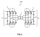
- FIG. 1 shows as an embodiment of the DC-DC converter a three-phase DC-DC converter G3 having a primary side 1 comprising three actively connected primary-side voltage bridges 11, 12, 13 each having two active switches S1 for converting a DC input voltage ES into primary-side AC voltages 111, 112, 113 for each of the primary-side voltage bridges 11, 12, 13 and a secondary side 2 comprising three actively connected secondary side voltage bridges 21, 22, 23 each having two active switches S2 for converting the secondary side AC voltages 211, 212, 213 for each of the secondary side voltage bridges 21, 22, 23 into a common DC Output voltage AS.
- Suitable switches S1, S2 for the voltage bridges are, for example, active semiconductor switches (power semiconductors) such as turn-off thyristors, transistors, MOSFETs, IGBTs (Insulated Gate Bipolar Transistors) or IGCTs (Integrated Gate-Commutated Thyristor) with intelligent GATE drivers.
- active semiconductor switches power semiconductors
- IGBTs Insulated Gate Bipolar Transistors
- IGCTs Integrated Gate-Commutated Thyristor
- the number of voltage bridges and / or the number of active switches S1, S2 per voltage bridge may vary, for example in an NPC topology with four switches per voltage bridge.
- Each of the primary-side voltage bridges 11, 12, 13 is connected to one of the secondary-side voltage bridges 21, 22, 23 via a multi-phase transformer 3, for example a three-phase transformer 3 in this case in the three-phase DC-DC converter G3, or via a respective separate transformer 3 to each one Phase coupled, wherein the primary side and secondary side applied AC voltages 111, 112, 113, 211, 212, 213 are shifted with a period T by a phase angle ⁇ .
- the phase angle of a first phase angle ⁇ 1 a second phase angle ⁇ 2 switched in the switching process.
- capacitors 10, 20 for smoothing the voltage are arranged on the primary side and on the secondary side.
- the capacitors may also be dispensed with or the capacitors may be replaced or supplemented by low-pass filters.
- the topology of the DC-DC converter shown here as a DAB DC / DC converter can be used for the switching methods according to the prior art as well as for the application of the switching method according to the invention. In other embodiments, the DC-DC converter may also have more than three phases for this purpose.
- the control unit for controlling the switches is not shown here.
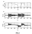
- Fig.2 shows the simulated traces of (a) phase angle in degrees, (b) phase current in amperes, and (c) DC current in amperes for a three-phase DC-DC converter Fig.1 with a switching method according to the prior art, which leads to oscillations in the DC current when the phase angle is changed rapidly. A quick change in the phase angle allows fast power transfers.
- the same values and assumptions became for the simulations for phase angle, phase current and DC current of the inventive method after Figure 3 and 5 represented in the FIGS. 4 and 6 used to achieve comparability of the illustrated behavior (prior art compared to the inventive method).
- the prior art switching method does not change the phase angle ⁇ of the three phases independently, but with a common step for all phases, as in FIG 2 (a) shown, causing strong oscillations of the DC current occur after each change of the phase angle ⁇ .
- the DC input current is shown here as an example of the DC input current, but qualitatively the same behavior also occurs in the DC output current.
- the time constant is proportional to L / R, where L denotes the sum of the leakage inductance of the primary winding and the primary leakage inductance of the secondary winding of the transformer, and R is the sum of the resistance of the primary winding and the primary side related resistance of the secondary winding.
- L denotes the sum of the leakage inductance of the primary winding and the primary leakage inductance of the secondary winding of the transformer
- R is the sum of the resistance of the primary winding and the primary side related resistance of the secondary winding.
- a high leakage inductance is of great importance for the use of this DAB DC / DC converter in a wide voltage range between primary and secondary voltage.
- a small resistance R is desirable to provide such a DAB DC / DC converter with low ohmic losses and high efficiency and thus higher efficiency. Due to these boundary conditions, the oscillations occurring after a power change have a long time constant.
- Figure 3 shows a first embodiment of the inventive method for a three-phase DAB DC / DC converter, with which the oscillations, as previously in Figure 2 (c) represented, can be avoided.
- the primary-side AC voltages 111, 112, 113 solid lines
- the secondary-side AC voltages 211, 212, 213 broken lines
- the DC input voltage is applied to the voltage bridges 11, 12, 13 with the active switches and is converted in the voltage bridges 11, 12, 13 by the circuit of the active switch S1 (switching operation) in an AC voltage 111, 112, 113 and in a corresponding AC voltage 211, 212, 213 transformed via the transformer 3.
- the switches S1 are usually turned on completely, arise at the output bridges 21, 22, 23 approximately rectangular alternating voltages 211, 212, 213 (square wave voltage).
- the voltage across the transformer windings thereby becomes step-shaped.
- the edges of the rectangular voltage 111, 112, 113, 211, 212, 213 are not infinitely steep due to the use of so-called snubbers, ie the shape deviates from the square-wave voltage (step shape at the transformer windings).
- the primary and secondary alternating voltages 111, 112, 113, 211, 212, 213 are switched by the switches S1, S2 in such a way that the switching process switches the (setting) of the phase angle ⁇ 2 for all three phases at the same edges of the primary and secondary-side AC voltage 111, 112, 113, 211, 212, 213 takes place on the primary and secondary voltage bridges, in each case on the falling edges of the AC voltages V1, V2 and V3 from ⁇ 1 to ⁇ 2, wherein the primary-side switching operation for the primary-side AC voltages 111th , 112, 113 for the second phase at time t0, for the third phase at time t0 + T / 3, and for the first phase at time t0 + 2/3 T.
- the switching operations for the secondary-side alternating voltages 211, 212, 213 occur in this embodiment relative to the circuits of the primary-side alternating voltages by ⁇ 1 or ⁇ 2 subsequently (shifted) depending on the edge orientation relative to the edge of the first circuit.
- the expression "below” denotes a positive phase angle ⁇ > 0.
- leading phase angles ⁇ corresponds to a negative phase angle ⁇ ⁇ 0.
- the circuits on the secondary side take place AC voltages 211, 213 of the first and third phases by ⁇ 2 lagging (shifted) for switching the corresponding primary-side AC voltages 111, 113 at the next falling edges of the secondary-side AC voltages 211, 213 of the first and third phases.
- the circuit in the case of previous rising flanks of the secondary-side alternating voltages 211, 213 of the first or third phases, the circuit, on the other hand, is delayed by ⁇ 1 in order to switch the corresponding primary-side alternating voltages 111, 113.
- the first switching 1 s2 of the primary-side (secondary-side) AC voltage 112 (212) of the second primary side (secondary side) voltage bridge 12 (22) takes place at the time t0 and the first switching 1 n2 of the secondary side (primary side) AC voltage 212 (112) of the second secondary side (primary-side) voltage bridges 22 (12) trailing at the phase angle ⁇ 2> 0, then the first switching 1 s1 of the primary-side (secondary-side) AC voltage 111 (211) of the first primary-side (secondary) voltage bridge 11 (21) takes place at time t0 + T / 6 and the first switching 1n1 of the secondary-side (primary-side) alternating voltage 211 (111) of the first secondary-side (primary-side) voltage bridge 21 (11) lagging independently of the previous switching with the phase angle ⁇ 1> 0, then the first switching 1s3 of the primary-side (secondary-side) AC voltage 113 (213) of the third primary-side
- the second switching 2s2 of the primary-side (secondary-side) AC voltage 112 (212) of the second primary-side (secondary-side) voltage bridge 12 (22) takes place at the time t0 + T / 2 and the second switching 2n2 of the secondary-side (primary-side) AC voltage 212 (112 ) of the second secondary-side (secondary-side) voltage bridge 22 (12) lagging independently of the previous circuits with the phase angle ⁇ 2> 0.
- the second switching 2s3 of the primary side (secondary side) AC voltage 113 (213) of the third primary side (secondary side) voltage bridge 13 (23) occurs at time t0 + 5/6 * T and the second switching 2n3 of the secondary-side (primary-side) AC voltage 213 (113) of the third secondary-side (primary-side) voltage bridge 23 (13) lagging independently of the previous circuits with a phase angle ⁇ 2> 0.
- the above switching method can alternatively also with negative phase angles are performed. In this case, the first or second switching of the secondary-side (primary-side) AC voltages would be leading (leading) for switching the primary-side (secondary) AC voltage.
- primary side and secondary side refer to circuits for current flow in the one direction of the DC-DC converter.
- the parenthesized numerals and designations "(primary side)” and “(secondary side)” refer to the corresponding circuits for the reverse current flow in the other direction of the DC-DC converter.
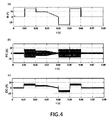
- Figure 4 shows the simulated traces of (a) phase angle in degrees, (b) phase current in amperes, and (c) DC current in amperes for a three-phase DC-DC converter Fig.1 , for the rapid change of the phase angle and to avoid oscillations of the DC current with the inventive switching method according to Figure 3 is operated.
- the phase current after T / 3 already reaches its nominal value and the DC current in Figure 4 (c) , does not show any of the oscillations necessary for a switching method according to the prior art Figure 2 (c) to see are.
- one or more capacitors may be arranged on the primary and / or secondary side for smoothing.
- FIG. 5 shows a to the switching method after Figure 3 alternative switching method according to the present invention.
- the switching operations for the secondary-side alternating voltages 211, 212, 213 take place in a change of the phase angle in two stages by ( ⁇ 1 + ⁇ 2) / 2 shifted alternately on falling and rising edges of the second, first and third phase - in the first circuit by ( ⁇ 1 + ⁇ 2) / 2 subsequently (shifted) and subsequently (shifted) in the second circuit by ⁇ 2.
- the primary-side AC voltages 111, 112, 113 solid lines
- the secondary-side AC voltages 211, 212, 213 broken lines
- the DC input voltage is applied to the voltage bridges 11, 12, 13 with the active switches and is converted in the voltage bridges 11, 12, 13 by the circuit of the active switch S1 (switching operation) in an AC voltage 111, 112, 113 and over the transformer connected to a corresponding AC voltage 211, 212, 213. Since the switches S1, S2 are generally switched on or off completely, approximately rectangular alternating voltages 111, 112, 113, 211, 212, 213 (FIG.
- the above steps are described as respective second switching 2s2, 2n2, 2s1, 2n1, 2s3, 2n3 of the primary side (secondary side) AC voltage 111, 112, 113 (211, 212, 213) and second lagging switching of the secondary side (primary side) AC voltage 211, 212, 213 (111, 112, 113) for the second, first and third primary and secondary voltage bridges 21, 22, 11, 12, 13, 23 to Setting the positive phase angle ⁇ 2 repeated.
- the above switching method can also be carried out with negative phase angles. In this case, the first or second switching of the secondary-side (primary-side) AC voltages would be leading (leading) for switching the primary-side (secondary) AC voltage.
- the non-bracket reference numerals and designations "primary side” and “secondary side” and the corresponding reference numerals refer to circuits for a current flow in the one direction of the DC-DC converter.
- the parenthesized designations "(primary side)” and “(secondary side)” refer to the corresponding circuits for the reverse current flow in the other direction of the DC-DC converter.
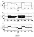
- Figure 6 shows the simulated traces of (a) phase angle in degrees, (b) phase current in amperes, and (c) DC current in amperes for a three-phase DC-DC converter Fig.1 , for the rapid change of the phase angle and to avoid oscillations of the DC current with the inventive switching method according to Figure 5 is operated.
- the phase current after T / 2 already reaches its nominal value and the DC current in Figure 6 (c) also does not show any of the oscillations necessary for a switching method according to the prior art Figure 2 (c) you can see.
- the phase current is in contrast to the method according to the invention Fig.
- one or more periods T of the primary-side and secondary-side AC voltages 111, 112, 113, 211, 212, 213 and where the phase angle ⁇ between the primary-side and secondary-side AC voltages 111, 112, 113, 211, 212, 213 on the flank is set step by step in several steps to the second phase angle ⁇ 2.
- the stepwise adjustment of the phase angle ⁇ 2 in steps of equal size can be linear.
- the phase angle .phi. Of the rising and falling edges in the switching operation can be adapted starting from the preceding phase angles for compensation of transformer and switch influences.
- the DC-DC converter G, G3 can be operated such that the phase shifts between the primary-side AC voltages 111, 112, 113 of the primary-side voltage bridges 11, 12, 13 with each other and the phase shifts between the secondary-side AC voltages 211, 212, 213 of the secondary-side voltage bridges 21, 22nd , 23 differ from each other by 120 °.
- Figure 7 shows a system according to the invention S DC-DC converter G and control unit 4, wherein the control unit 4 is configured to control the active switch S1, S2 of the primary and secondary side voltage bridges 11, 12, 13, 21, 22, 23 of the at least three-phase DC-DC converter G. according to the inventive method, as exemplified in the Fig. 3 and 5 shown for a three-phase DC-DC converter to execute.
- the DC-DC converter G is a three-phase DC-DC converter with three actively connected primary-side voltage bridges 11, 12, 13 each having two or more active switches S1 and three actively connected secondary-side voltage bridges 21, 22, 23 each having two or more active switches S2.
- control unit 4 may, at the option of the person skilled in the art, as the controller 4 using one or more DSPs (digital signal processor), FPGAs (so-called “field programmable gate arrays”), CLPDs (so-called “complex programmable logic devices”), a Microcontroller or using be performed a combination of the above components.
- DSPs digital signal processor
- FPGAs field programmable gate arrays
- CLPDs complex programmable logic devices
Landscapes
- Engineering & Computer Science (AREA)
- Power Engineering (AREA)
- Dc-Dc Converters (AREA)
Applications Claiming Priority (2)
| Application Number | Priority Date | Filing Date | Title |
|---|---|---|---|
| DE102012204035A DE102012204035A1 (de) | 2012-03-14 | 2012-03-14 | Stromregelung für Gleichspannungswandler |
| PCT/EP2013/055230 WO2013135811A2 (de) | 2012-03-14 | 2013-03-14 | Stromregelung für gleichspannungswandler |
Publications (2)
| Publication Number | Publication Date |
|---|---|
| EP2826139A2 EP2826139A2 (de) | 2015-01-21 |
| EP2826139B1 true EP2826139B1 (de) | 2016-07-20 |
Family
ID=47882163
Family Applications (1)
| Application Number | Title | Priority Date | Filing Date |
|---|---|---|---|
| EP13709207.8A Not-in-force EP2826139B1 (de) | 2012-03-14 | 2013-03-14 | Stromregelung für gleichspannungswandler |
Country Status (8)
| Country | Link |
|---|---|
| US (1) | US9825532B2 (ko) |
| EP (1) | EP2826139B1 (ko) |
| KR (1) | KR102207433B1 (ko) |
| CN (1) | CN104170231B (ko) |
| DE (1) | DE102012204035A1 (ko) |
| HK (1) | HK1200605A1 (ko) |
| IN (1) | IN2014MN01826A (ko) |
| WO (1) | WO2013135811A2 (ko) |
Cited By (1)
| Publication number | Priority date | Publication date | Assignee | Title |
|---|---|---|---|---|
| DE102017201667A1 (de) | 2017-02-02 | 2018-08-02 | Rheinisch-Westfälische Technische Hochschule Aachen (RWTH) | Hochdynamische Steuerung von Multiport-DAB-Wandlern |
Families Citing this family (18)
| Publication number | Priority date | Publication date | Assignee | Title |
|---|---|---|---|---|
| EP2884614A1 (en) | 2013-12-13 | 2015-06-17 | Alstom Renovables España, S.L. | Multiphase generator-conversion systems |
| JP6003932B2 (ja) * | 2014-03-11 | 2016-10-05 | トヨタ自動車株式会社 | 電力変換装置及びその起動方法 |
| US9802493B2 (en) * | 2014-06-20 | 2017-10-31 | Cooper Technologies Company | Multi-phase bidirectional DC to DC power converter circuits, systems and methods with transient stress control |
| DE102014214542A1 (de) * | 2014-07-24 | 2016-02-11 | Rheinisch-Westfälisch-Technische Hochschule Aachen | Gleichspannungswandler mit Transformator |
| EP3104509A1 (en) * | 2015-06-09 | 2016-12-14 | Constructions Electroniques + Telecommunications | Dual bridge dc/dc power converter |
| DE102015109967A1 (de) | 2015-06-22 | 2016-12-22 | Gip Ag | Vorrichtung und Verfahren zum bidirektionalen Verbinden zweier Stromnetze |
| WO2017123241A1 (en) | 2016-01-15 | 2017-07-20 | General Electric Company | System and method for operating a dc to dc power converter |
| CN105958830A (zh) * | 2016-06-06 | 2016-09-21 | 西安交通大学 | 一种电流最优调制下三相双有源桥式直流变换器的控制方法 |
| EP3320612A1 (en) | 2016-07-07 | 2018-05-16 | Huawei Technologies Co., Ltd. | Four-switch three phase dc-dc resonant converter |
| KR101883562B1 (ko) * | 2016-10-26 | 2018-07-30 | 한국전력공사 | Dab 컨버터의 상전류 제어 장치 및 그 방법 |
| CN106787752A (zh) * | 2016-12-26 | 2017-05-31 | 东北电力大学 | 基于三相双主动桥式dc‑dc变换器的光伏并网系统 |
| US11356015B2 (en) * | 2017-05-10 | 2022-06-07 | North Carolina State University | Modular medium voltage fast chargers |
| US11777433B2 (en) * | 2018-03-16 | 2023-10-03 | Melexis Bulgaria Ltd. | Driver and method for low inductance motor |
| DE102018204413A1 (de) * | 2018-03-22 | 2019-09-26 | Rheinisch-Westfälische Technische Hochschule (Rwth) Aachen | Regelung von Sättigungseffekten von Transformatoren |
| DE102018210806A1 (de) * | 2018-06-29 | 2020-01-02 | Rheinisch-Westfälische Technische Hochschule (Rwth) Aachen | Elektrische Schaltung mit Hilfsspannungsquelle für Zero-Voltage-Switching in einem Gleichspannungswandler unter sämtlichen Lastbedingungen |
| DE102020106660A1 (de) * | 2019-03-19 | 2020-09-24 | Brusa Elektronik Ag | Verfahren zum Betreiben eines elektronischen Leistungswandlers und elektronischer Leistungswandler |
| CN111446864A (zh) * | 2020-04-24 | 2020-07-24 | 深圳威迈斯新能源股份有限公司 | 一种多相dc/dc并联控制方法及其控制电路 |
| EP4012871B1 (de) | 2020-12-08 | 2023-06-07 | Gip Ag | Verfahren zum gerichteten übertragen von energie in form von energiepaketen |
Family Cites Families (10)
| Publication number | Priority date | Publication date | Assignee | Title |
|---|---|---|---|---|
| US5027264A (en) | 1989-09-29 | 1991-06-25 | Wisconsin Alumni Research Foundation | Power conversion apparatus for DC/DC conversion using dual active bridges |
| US5355294A (en) * | 1992-11-25 | 1994-10-11 | General Electric Company | Unity power factor control for dual active bridge converter |
| US6370050B1 (en) * | 1999-09-20 | 2002-04-09 | Ut-Batelle, Llc | Isolated and soft-switched power converter |
| JP2004096953A (ja) * | 2002-09-03 | 2004-03-25 | Sumitomo Heavy Ind Ltd | 電力変換器 |
| US7408794B2 (en) * | 2006-02-21 | 2008-08-05 | Ut-Battele Llc | Triple voltage dc-to-dc converter and method |
| CN100571006C (zh) * | 2006-05-16 | 2009-12-16 | 中国科学院电工研究所 | 超导储能用双向三电平软开关dc/dc变换器及其控制方法 |
| US8587975B2 (en) * | 2010-04-01 | 2013-11-19 | Arizona Board Of Regents For And On Behalf Of Arizona State University | PWM control of dual active bridge converters |
| KR101168078B1 (ko) * | 2010-12-17 | 2012-07-24 | 한국에너지기술연구원 | 다중입력 양방향 dc-dc 컨버터 |
| CN102064707B (zh) * | 2011-01-21 | 2013-02-27 | 浙江大学 | 共同移相角控制下的输入并联输出并联组合变换器 |
| CN102136729B (zh) * | 2011-02-22 | 2014-08-06 | 西安交通大学 | 一种基于移相多绕组整流变压器的串联多电平svg拓扑结构及其控制方法 |
-
2012
- 2012-03-14 DE DE102012204035A patent/DE102012204035A1/de not_active Ceased
-
2013
- 2013-03-14 EP EP13709207.8A patent/EP2826139B1/de not_active Not-in-force
- 2013-03-14 WO PCT/EP2013/055230 patent/WO2013135811A2/de active Application Filing
- 2013-03-14 IN IN1826MUN2014 patent/IN2014MN01826A/en unknown
- 2013-03-14 KR KR1020147028269A patent/KR102207433B1/ko active IP Right Grant
- 2013-03-14 US US14/380,304 patent/US9825532B2/en not_active Expired - Fee Related
- 2013-03-14 CN CN201380014281.XA patent/CN104170231B/zh not_active Expired - Fee Related
-
2015
- 2015-01-23 HK HK15100750.3A patent/HK1200605A1/zh not_active IP Right Cessation
Cited By (1)
| Publication number | Priority date | Publication date | Assignee | Title |
|---|---|---|---|---|
| DE102017201667A1 (de) | 2017-02-02 | 2018-08-02 | Rheinisch-Westfälische Technische Hochschule Aachen (RWTH) | Hochdynamische Steuerung von Multiport-DAB-Wandlern |
Also Published As
| Publication number | Publication date |
|---|---|
| US20150146455A1 (en) | 2015-05-28 |
| WO2013135811A2 (de) | 2013-09-19 |
| DE102012204035A1 (de) | 2013-09-19 |
| US9825532B2 (en) | 2017-11-21 |
| CN104170231B (zh) | 2017-03-08 |
| KR102207433B1 (ko) | 2021-01-26 |
| CN104170231A (zh) | 2014-11-26 |
| EP2826139A2 (de) | 2015-01-21 |
| KR20140135237A (ko) | 2014-11-25 |
| WO2013135811A3 (de) | 2014-04-24 |
| HK1200605A1 (zh) | 2015-08-07 |
| IN2014MN01826A (ko) | 2015-07-03 |
Similar Documents
| Publication | Publication Date | Title |
|---|---|---|
| EP2826139B1 (de) | Stromregelung für gleichspannungswandler | |
| EP3172823B1 (de) | Gleichspannungswandler mit transformator | |
| EP1882299B1 (de) | Bidirektionaler batteriewechselrichter | |
| EP2671313B1 (de) | Gegentaktwandler und modulationsverfahren zum ansteuern eines gegentaktwandlers | |
| DE102017212224B4 (de) | Hochspannungsgenerator für ein Röntgengerät | |
| EP2495858A1 (de) | Bidirektionaler Gleichspannungswandler | |
| CH698835B1 (de) | Eigenstromversorgung für Stromrichterschaltertreiber. | |
| WO2006000111A1 (de) | Oberschwingungsarme mehrphasige umrichterschaltung | |
| DE102018210806A1 (de) | Elektrische Schaltung mit Hilfsspannungsquelle für Zero-Voltage-Switching in einem Gleichspannungswandler unter sämtlichen Lastbedingungen | |
| EP3563475B1 (de) | Stromrichterschaltung und verfahren zur steuerung derselben | |
| WO2012131073A2 (de) | Verfahren zur erzeugung einer ausgangsspannung und anordnung zur durchführung des verfahrens | |
| DE102018210807A1 (de) | Elektrische Schaltung für Zero-Voltage-Soft-Switching in einem Gleichspannungswandler | |
| DE102013005277B3 (de) | Verfahren zum Umwandeln von Gleichspannung in Wechselspannung und Wechselrichterschaltung dafür | |
| EP3913786A1 (de) | Stromrichteranordnung mit einem netzgeführten stromrichter sowie verfahren zum anfahren der stromrichteranordnung | |
| AT519842A1 (de) | Wechselrichter | |
| EP3652848B1 (de) | Resonanter gleichstromsteller | |
| DE102014203404B4 (de) | Stromrichterschaltung und Verfahren zum Betreiben derselben | |
| DE202017007018U1 (de) | Vorrichtung zum Starten eines Dreiphasen-Multiport-Active-Bridge-Gleichspannungswandlers | |
| DE102017201667A1 (de) | Hochdynamische Steuerung von Multiport-DAB-Wandlern | |
| CH707447A2 (de) | Vorrichtung zur Gleichspannungswandlung für hohe Übersetzungsverhältnisse. | |
| EP3360241B1 (de) | Gleichspannungswandler und verfahren zum betrieb eines gleichspannungswandlers | |
| EP3291433A1 (de) | Gleichspannungswandler mit transformator | |
| WO2017028988A1 (de) | Dreiphasiger gleichspannungswandler | |
| WO2023006949A1 (de) | Stromrichterschaltung zum erzeugen einer potentialgetrennten gleichspannung | |
| EP4170883A1 (de) | Verfahren zur regelung eines resonanzwandlers |
Legal Events
| Date | Code | Title | Description |
|---|---|---|---|
| PUAI | Public reference made under article 153(3) epc to a published international application that has entered the european phase |
Free format text: ORIGINAL CODE: 0009012 |
|
| 17P | Request for examination filed |
Effective date: 20141024 |
|
| AK | Designated contracting states |
Kind code of ref document: A2 Designated state(s): AL AT BE BG CH CY CZ DE DK EE ES FI FR GB GR HR HU IE IS IT LI LT LU LV MC MK MT NL NO PL PT RO RS SE SI SK SM TR |
|
| AX | Request for extension of the european patent |
Extension state: BA ME |
|
| DAX | Request for extension of the european patent (deleted) | ||
| REG | Reference to a national code |
Ref country code: HK Ref legal event code: DE Ref document number: 1200605 Country of ref document: HK |
|
| 17Q | First examination report despatched |
Effective date: 20151005 |
|
| GRAJ | Information related to disapproval of communication of intention to grant by the applicant or resumption of examination proceedings by the epo deleted |
Free format text: ORIGINAL CODE: EPIDOSDIGR1 |
|
| GRAP | Despatch of communication of intention to grant a patent |
Free format text: ORIGINAL CODE: EPIDOSNIGR1 |
|
| GRAP | Despatch of communication of intention to grant a patent |
Free format text: ORIGINAL CODE: EPIDOSNIGR1 |
|
| INTG | Intention to grant announced |
Effective date: 20160330 |
|
| RAP1 | Party data changed (applicant data changed or rights of an application transferred) |
Owner name: FLEXIBLE ELEKTRISCHE NETZE FEN GMBH |
|
| GRAS | Grant fee paid |
Free format text: ORIGINAL CODE: EPIDOSNIGR3 |
|
| GRAA | (expected) grant |
Free format text: ORIGINAL CODE: 0009210 |
|
| GRAF | Information related to payment of grant fee modified |
Free format text: ORIGINAL CODE: EPIDOSCIGR3 |
|
| AK | Designated contracting states |
Kind code of ref document: B1 Designated state(s): AL AT BE BG CH CY CZ DE DK EE ES FI FR GB GR HR HU IE IS IT LI LT LU LV MC MK MT NL NO PL PT RO RS SE SI SK SM TR |
|
| REG | Reference to a national code |
Ref country code: GB Ref legal event code: FG4D Free format text: NOT ENGLISH |
|
| REG | Reference to a national code |
Ref country code: CH Ref legal event code: EP |
|
| REG | Reference to a national code |
Ref country code: IE Ref legal event code: FG4D Free format text: LANGUAGE OF EP DOCUMENT: GERMAN |
|
| REG | Reference to a national code |
Ref country code: CH Ref legal event code: NV Representative=s name: R.A. EGLI AND CO, PATENTANWAELTE, CH Ref country code: AT Ref legal event code: REF Ref document number: 814785 Country of ref document: AT Kind code of ref document: T Effective date: 20160815 |
|
| REG | Reference to a national code |
Ref country code: DE Ref legal event code: R096 Ref document number: 502013003792 Country of ref document: DE |
|
| REG | Reference to a national code |
Ref country code: NL Ref legal event code: FP |
|
| REG | Reference to a national code |
Ref country code: SE Ref legal event code: TRGR |
|
| REG | Reference to a national code |
Ref country code: LT Ref legal event code: MG4D |
|
| PG25 | Lapsed in a contracting state [announced via postgrant information from national office to epo] |
Ref country code: HR Free format text: LAPSE BECAUSE OF FAILURE TO SUBMIT A TRANSLATION OF THE DESCRIPTION OR TO PAY THE FEE WITHIN THE PRESCRIBED TIME-LIMIT Effective date: 20160720 Ref country code: NO Free format text: LAPSE BECAUSE OF FAILURE TO SUBMIT A TRANSLATION OF THE DESCRIPTION OR TO PAY THE FEE WITHIN THE PRESCRIBED TIME-LIMIT Effective date: 20161020 Ref country code: IS Free format text: LAPSE BECAUSE OF FAILURE TO SUBMIT A TRANSLATION OF THE DESCRIPTION OR TO PAY THE FEE WITHIN THE PRESCRIBED TIME-LIMIT Effective date: 20161120 Ref country code: RS Free format text: LAPSE BECAUSE OF FAILURE TO SUBMIT A TRANSLATION OF THE DESCRIPTION OR TO PAY THE FEE WITHIN THE PRESCRIBED TIME-LIMIT Effective date: 20160720 Ref country code: FI Free format text: LAPSE BECAUSE OF FAILURE TO SUBMIT A TRANSLATION OF THE DESCRIPTION OR TO PAY THE FEE WITHIN THE PRESCRIBED TIME-LIMIT Effective date: 20160720 Ref country code: LT Free format text: LAPSE BECAUSE OF FAILURE TO SUBMIT A TRANSLATION OF THE DESCRIPTION OR TO PAY THE FEE WITHIN THE PRESCRIBED TIME-LIMIT Effective date: 20160720 |
|
| PG25 | Lapsed in a contracting state [announced via postgrant information from national office to epo] |
Ref country code: PL Free format text: LAPSE BECAUSE OF FAILURE TO SUBMIT A TRANSLATION OF THE DESCRIPTION OR TO PAY THE FEE WITHIN THE PRESCRIBED TIME-LIMIT Effective date: 20160720 Ref country code: LV Free format text: LAPSE BECAUSE OF FAILURE TO SUBMIT A TRANSLATION OF THE DESCRIPTION OR TO PAY THE FEE WITHIN THE PRESCRIBED TIME-LIMIT Effective date: 20160720 Ref country code: PT Free format text: LAPSE BECAUSE OF FAILURE TO SUBMIT A TRANSLATION OF THE DESCRIPTION OR TO PAY THE FEE WITHIN THE PRESCRIBED TIME-LIMIT Effective date: 20161121 Ref country code: ES Free format text: LAPSE BECAUSE OF FAILURE TO SUBMIT A TRANSLATION OF THE DESCRIPTION OR TO PAY THE FEE WITHIN THE PRESCRIBED TIME-LIMIT Effective date: 20160720 Ref country code: GR Free format text: LAPSE BECAUSE OF FAILURE TO SUBMIT A TRANSLATION OF THE DESCRIPTION OR TO PAY THE FEE WITHIN THE PRESCRIBED TIME-LIMIT Effective date: 20161021 |
|
| REG | Reference to a national code |
Ref country code: FR Ref legal event code: PLFP Year of fee payment: 5 |
|
| REG | Reference to a national code |
Ref country code: DE Ref legal event code: R097 Ref document number: 502013003792 Country of ref document: DE |
|
| PG25 | Lapsed in a contracting state [announced via postgrant information from national office to epo] |
Ref country code: EE Free format text: LAPSE BECAUSE OF FAILURE TO SUBMIT A TRANSLATION OF THE DESCRIPTION OR TO PAY THE FEE WITHIN THE PRESCRIBED TIME-LIMIT Effective date: 20160720 Ref country code: RO Free format text: LAPSE BECAUSE OF FAILURE TO SUBMIT A TRANSLATION OF THE DESCRIPTION OR TO PAY THE FEE WITHIN THE PRESCRIBED TIME-LIMIT Effective date: 20160720 |
|
| PLBE | No opposition filed within time limit |
Free format text: ORIGINAL CODE: 0009261 |
|
| STAA | Information on the status of an ep patent application or granted ep patent |
Free format text: STATUS: NO OPPOSITION FILED WITHIN TIME LIMIT |
|
| PG25 | Lapsed in a contracting state [announced via postgrant information from national office to epo] |
Ref country code: SM Free format text: LAPSE BECAUSE OF FAILURE TO SUBMIT A TRANSLATION OF THE DESCRIPTION OR TO PAY THE FEE WITHIN THE PRESCRIBED TIME-LIMIT Effective date: 20160720 Ref country code: DK Free format text: LAPSE BECAUSE OF FAILURE TO SUBMIT A TRANSLATION OF THE DESCRIPTION OR TO PAY THE FEE WITHIN THE PRESCRIBED TIME-LIMIT Effective date: 20160720 Ref country code: SK Free format text: LAPSE BECAUSE OF FAILURE TO SUBMIT A TRANSLATION OF THE DESCRIPTION OR TO PAY THE FEE WITHIN THE PRESCRIBED TIME-LIMIT Effective date: 20160720 Ref country code: CZ Free format text: LAPSE BECAUSE OF FAILURE TO SUBMIT A TRANSLATION OF THE DESCRIPTION OR TO PAY THE FEE WITHIN THE PRESCRIBED TIME-LIMIT Effective date: 20160720 Ref country code: BG Free format text: LAPSE BECAUSE OF FAILURE TO SUBMIT A TRANSLATION OF THE DESCRIPTION OR TO PAY THE FEE WITHIN THE PRESCRIBED TIME-LIMIT Effective date: 20161020 |
|
| 26N | No opposition filed |
Effective date: 20170421 |
|
| REG | Reference to a national code |
Ref country code: HK Ref legal event code: GR Ref document number: 1200605 Country of ref document: HK |
|
| PG25 | Lapsed in a contracting state [announced via postgrant information from national office to epo] |
Ref country code: SI Free format text: LAPSE BECAUSE OF FAILURE TO SUBMIT A TRANSLATION OF THE DESCRIPTION OR TO PAY THE FEE WITHIN THE PRESCRIBED TIME-LIMIT Effective date: 20160720 |
|
| PG25 | Lapsed in a contracting state [announced via postgrant information from national office to epo] |
Ref country code: MC Free format text: LAPSE BECAUSE OF FAILURE TO SUBMIT A TRANSLATION OF THE DESCRIPTION OR TO PAY THE FEE WITHIN THE PRESCRIBED TIME-LIMIT Effective date: 20160720 |
|
| REG | Reference to a national code |
Ref country code: IE Ref legal event code: MM4A |
|
| PG25 | Lapsed in a contracting state [announced via postgrant information from national office to epo] |
Ref country code: LU Free format text: LAPSE BECAUSE OF NON-PAYMENT OF DUE FEES Effective date: 20170314 |
|
| PG25 | Lapsed in a contracting state [announced via postgrant information from national office to epo] |
Ref country code: IE Free format text: LAPSE BECAUSE OF NON-PAYMENT OF DUE FEES Effective date: 20170314 |
|
| REG | Reference to a national code |
Ref country code: FR Ref legal event code: PLFP Year of fee payment: 6 |
|
| PG25 | Lapsed in a contracting state [announced via postgrant information from national office to epo] |
Ref country code: MT Free format text: LAPSE BECAUSE OF FAILURE TO SUBMIT A TRANSLATION OF THE DESCRIPTION OR TO PAY THE FEE WITHIN THE PRESCRIBED TIME-LIMIT Effective date: 20160720 |
|
| PG25 | Lapsed in a contracting state [announced via postgrant information from national office to epo] |
Ref country code: AL Free format text: LAPSE BECAUSE OF FAILURE TO SUBMIT A TRANSLATION OF THE DESCRIPTION OR TO PAY THE FEE WITHIN THE PRESCRIBED TIME-LIMIT Effective date: 20160720 |
|
| PGFP | Annual fee paid to national office [announced via postgrant information from national office to epo] |
Ref country code: RO Payment date: 20190325 Year of fee payment: 7 Ref country code: FR Payment date: 20190322 Year of fee payment: 7 Ref country code: GB Payment date: 20190320 Year of fee payment: 7 Ref country code: CH Payment date: 20190320 Year of fee payment: 7 |
|
| PGFP | Annual fee paid to national office [announced via postgrant information from national office to epo] |
Ref country code: NL Payment date: 20190320 Year of fee payment: 7 Ref country code: SE Payment date: 20190320 Year of fee payment: 7 Ref country code: AT Payment date: 20190321 Year of fee payment: 7 Ref country code: BE Payment date: 20190320 Year of fee payment: 7 |
|
| PG25 | Lapsed in a contracting state [announced via postgrant information from national office to epo] |
Ref country code: HU Free format text: LAPSE BECAUSE OF FAILURE TO SUBMIT A TRANSLATION OF THE DESCRIPTION OR TO PAY THE FEE WITHIN THE PRESCRIBED TIME-LIMIT; INVALID AB INITIO Effective date: 20130314 |
|
| PG25 | Lapsed in a contracting state [announced via postgrant information from national office to epo] |
Ref country code: CY Free format text: LAPSE BECAUSE OF FAILURE TO SUBMIT A TRANSLATION OF THE DESCRIPTION OR TO PAY THE FEE WITHIN THE PRESCRIBED TIME-LIMIT Effective date: 20160720 |
|
| PG25 | Lapsed in a contracting state [announced via postgrant information from national office to epo] |
Ref country code: MK Free format text: LAPSE BECAUSE OF FAILURE TO SUBMIT A TRANSLATION OF THE DESCRIPTION OR TO PAY THE FEE WITHIN THE PRESCRIBED TIME-LIMIT Effective date: 20160720 |
|
| PG25 | Lapsed in a contracting state [announced via postgrant information from national office to epo] |
Ref country code: TR Free format text: LAPSE BECAUSE OF FAILURE TO SUBMIT A TRANSLATION OF THE DESCRIPTION OR TO PAY THE FEE WITHIN THE PRESCRIBED TIME-LIMIT Effective date: 20160720 |
|
| REG | Reference to a national code |
Ref country code: CH Ref legal event code: PL |
|
| REG | Reference to a national code |
Ref country code: NL Ref legal event code: MM Effective date: 20200401 |
|
| REG | Reference to a national code |
Ref country code: AT Ref legal event code: MM01 Ref document number: 814785 Country of ref document: AT Kind code of ref document: T Effective date: 20200314 |
|
| REG | Reference to a national code |
Ref country code: BE Ref legal event code: MM Effective date: 20200331 |
|
| PG25 | Lapsed in a contracting state [announced via postgrant information from national office to epo] |
Ref country code: NL Free format text: LAPSE BECAUSE OF NON-PAYMENT OF DUE FEES Effective date: 20200401 |
|
| PG25 | Lapsed in a contracting state [announced via postgrant information from national office to epo] |
Ref country code: SE Free format text: LAPSE BECAUSE OF NON-PAYMENT OF DUE FEES Effective date: 20200315 Ref country code: LI Free format text: LAPSE BECAUSE OF NON-PAYMENT OF DUE FEES Effective date: 20200331 Ref country code: FR Free format text: LAPSE BECAUSE OF NON-PAYMENT OF DUE FEES Effective date: 20200331 Ref country code: AT Free format text: LAPSE BECAUSE OF NON-PAYMENT OF DUE FEES Effective date: 20200314 Ref country code: CH Free format text: LAPSE BECAUSE OF NON-PAYMENT OF DUE FEES Effective date: 20200331 |
|
| PG25 | Lapsed in a contracting state [announced via postgrant information from national office to epo] |
Ref country code: BE Free format text: LAPSE BECAUSE OF NON-PAYMENT OF DUE FEES Effective date: 20200331 |
|
| GBPC | Gb: european patent ceased through non-payment of renewal fee |
Effective date: 20200314 |
|
| PG25 | Lapsed in a contracting state [announced via postgrant information from national office to epo] |
Ref country code: GB Free format text: LAPSE BECAUSE OF NON-PAYMENT OF DUE FEES Effective date: 20200314 |
|
| PGFP | Annual fee paid to national office [announced via postgrant information from national office to epo] |
Ref country code: DE Payment date: 20210331 Year of fee payment: 9 |
|
| PG25 | Lapsed in a contracting state [announced via postgrant information from national office to epo] |
Ref country code: IT Free format text: LAPSE BECAUSE OF NON-PAYMENT OF DUE FEES Effective date: 20200314 |
|
| REG | Reference to a national code |
Ref country code: DE Ref legal event code: R119 Ref document number: 502013003792 Country of ref document: DE |
|
| PG25 | Lapsed in a contracting state [announced via postgrant information from national office to epo] |
Ref country code: DE Free format text: LAPSE BECAUSE OF NON-PAYMENT OF DUE FEES Effective date: 20221001 |