EP2822046B1 - Dispositif électroluminescent - Google Patents
Dispositif électroluminescent Download PDFInfo
- Publication number
- EP2822046B1 EP2822046B1 EP14174704.8A EP14174704A EP2822046B1 EP 2822046 B1 EP2822046 B1 EP 2822046B1 EP 14174704 A EP14174704 A EP 14174704A EP 2822046 B1 EP2822046 B1 EP 2822046B1
- Authority
- EP
- European Patent Office
- Prior art keywords
- light emitting
- light
- emitting device
- wiring portions
- base member
- Prior art date
- Legal status (The legal status is an assumption and is not a legal conclusion. Google has not performed a legal analysis and makes no representation as to the accuracy of the status listed.)
- Active
Links
- 239000000463 material Substances 0.000 claims description 60
- 229920005989 resin Polymers 0.000 claims description 29
- 239000011347 resin Substances 0.000 claims description 29
- 239000000853 adhesive Substances 0.000 claims description 20
- 239000004642 Polyimide Substances 0.000 claims description 13
- 229920001721 polyimide Polymers 0.000 claims description 13
- 230000031700 light absorption Effects 0.000 claims description 9
- 239000006229 carbon black Substances 0.000 claims description 5
- 230000003287 optical effect Effects 0.000 claims description 4
- 229920000139 polyethylene terephthalate Polymers 0.000 claims description 4
- 239000005020 polyethylene terephthalate Substances 0.000 claims description 4
- 239000011112 polyethylene naphthalate Substances 0.000 claims description 2
- -1 polyethylene terephthalate Polymers 0.000 claims description 2
- 238000002834 transmittance Methods 0.000 claims 1
- 239000000758 substrate Substances 0.000 description 32
- 238000007789 sealing Methods 0.000 description 17
- GWEVSGVZZGPLCZ-UHFFFAOYSA-N Titan oxide Chemical compound O=[Ti]=O GWEVSGVZZGPLCZ-UHFFFAOYSA-N 0.000 description 6
- 230000006866 deterioration Effects 0.000 description 5
- 238000000605 extraction Methods 0.000 description 5
- 229920002050 silicone resin Polymers 0.000 description 5
- VYPSYNLAJGMNEJ-UHFFFAOYSA-N Silicium dioxide Chemical compound O=[Si]=O VYPSYNLAJGMNEJ-UHFFFAOYSA-N 0.000 description 4
- TZCXTZWJZNENPQ-UHFFFAOYSA-L barium sulfate Chemical compound [Ba+2].[O-]S([O-])(=O)=O TZCXTZWJZNENPQ-UHFFFAOYSA-L 0.000 description 4
- OGIDPMRJRNCKJF-UHFFFAOYSA-N titanium oxide Inorganic materials [Ti]=O OGIDPMRJRNCKJF-UHFFFAOYSA-N 0.000 description 4
- 229910052751 metal Inorganic materials 0.000 description 3
- 239000002184 metal Substances 0.000 description 3
- 239000004065 semiconductor Substances 0.000 description 3
- 229910000679 solder Inorganic materials 0.000 description 3
- RYGMFSIKBFXOCR-UHFFFAOYSA-N Copper Chemical compound [Cu] RYGMFSIKBFXOCR-UHFFFAOYSA-N 0.000 description 2
- 239000004593 Epoxy Substances 0.000 description 2
- 229910002601 GaN Inorganic materials 0.000 description 2
- JMASRVWKEDWRBT-UHFFFAOYSA-N Gallium nitride Chemical compound [Ga]#N JMASRVWKEDWRBT-UHFFFAOYSA-N 0.000 description 2
- CPLXHLVBOLITMK-UHFFFAOYSA-N Magnesium oxide Chemical compound [Mg]=O CPLXHLVBOLITMK-UHFFFAOYSA-N 0.000 description 2
- UCKMPCXJQFINFW-UHFFFAOYSA-N Sulphide Chemical compound [S-2] UCKMPCXJQFINFW-UHFFFAOYSA-N 0.000 description 2
- MCMNRKCIXSYSNV-UHFFFAOYSA-N Zirconium dioxide Chemical compound O=[Zr]=O MCMNRKCIXSYSNV-UHFFFAOYSA-N 0.000 description 2
- 230000001070 adhesive effect Effects 0.000 description 2
- 229910052782 aluminium Inorganic materials 0.000 description 2
- XAGFODPZIPBFFR-UHFFFAOYSA-N aluminium Chemical compound [Al] XAGFODPZIPBFFR-UHFFFAOYSA-N 0.000 description 2
- PNEYBMLMFCGWSK-UHFFFAOYSA-N aluminium oxide Inorganic materials [O-2].[O-2].[O-2].[Al+3].[Al+3] PNEYBMLMFCGWSK-UHFFFAOYSA-N 0.000 description 2
- 230000015556 catabolic process Effects 0.000 description 2
- 239000011889 copper foil Substances 0.000 description 2
- 238000006731 degradation reaction Methods 0.000 description 2
- 230000000694 effects Effects 0.000 description 2
- 238000005516 engineering process Methods 0.000 description 2
- 239000003822 epoxy resin Substances 0.000 description 2
- 239000000945 filler Substances 0.000 description 2
- 239000011888 foil Substances 0.000 description 2
- 239000011810 insulating material Substances 0.000 description 2
- 150000004767 nitrides Chemical class 0.000 description 2
- 229920000647 polyepoxide Polymers 0.000 description 2
- 229910052814 silicon oxide Inorganic materials 0.000 description 2
- 229910017944 Ag—Cu Inorganic materials 0.000 description 1
- 229910015363 Au—Sn Inorganic materials 0.000 description 1
- 229910020888 Sn-Cu Inorganic materials 0.000 description 1
- 229910008433 SnCU Inorganic materials 0.000 description 1
- 229910019204 Sn—Cu Inorganic materials 0.000 description 1
- 229920001807 Urea-formaldehyde Polymers 0.000 description 1
- NIXOWILDQLNWCW-UHFFFAOYSA-N acrylic acid group Chemical group C(C=C)(=O)O NIXOWILDQLNWCW-UHFFFAOYSA-N 0.000 description 1
- 230000002411 adverse Effects 0.000 description 1
- 150000001408 amides Chemical class 0.000 description 1
- 238000000149 argon plasma sintering Methods 0.000 description 1
- 238000005452 bending Methods 0.000 description 1
- 239000003795 chemical substances by application Substances 0.000 description 1
- 229910052681 coesite Inorganic materials 0.000 description 1
- 239000003086 colorant Substances 0.000 description 1
- 239000010949 copper Substances 0.000 description 1
- 229910052593 corundum Inorganic materials 0.000 description 1
- 229910052906 cristobalite Inorganic materials 0.000 description 1
- 238000000354 decomposition reaction Methods 0.000 description 1
- 238000002845 discoloration Methods 0.000 description 1
- 238000010292 electrical insulation Methods 0.000 description 1
- 239000011521 glass Substances 0.000 description 1
- 230000017525 heat dissipation Effects 0.000 description 1
- 125000005462 imide group Chemical group 0.000 description 1
- 150000003949 imides Chemical class 0.000 description 1
- 230000001678 irradiating effect Effects 0.000 description 1
- 239000004973 liquid crystal related substance Substances 0.000 description 1
- 230000007257 malfunction Effects 0.000 description 1
- 238000004519 manufacturing process Methods 0.000 description 1
- TWNQGVIAIRXVLR-UHFFFAOYSA-N oxo(oxoalumanyloxy)alumane Chemical compound O=[Al]O[Al]=O TWNQGVIAIRXVLR-UHFFFAOYSA-N 0.000 description 1
- 239000000049 pigment Substances 0.000 description 1
- 229920001296 polysiloxane Polymers 0.000 description 1
- 239000011148 porous material Substances 0.000 description 1
- 238000003672 processing method Methods 0.000 description 1
- 238000009877 rendering Methods 0.000 description 1
- 229910052594 sapphire Inorganic materials 0.000 description 1
- 239000010980 sapphire Substances 0.000 description 1
- 238000000926 separation method Methods 0.000 description 1
- 239000000377 silicon dioxide Substances 0.000 description 1
- 229910052682 stishovite Inorganic materials 0.000 description 1
- 229920001187 thermosetting polymer Polymers 0.000 description 1
- 229910052905 tridymite Inorganic materials 0.000 description 1
- 229910001845 yogo sapphire Inorganic materials 0.000 description 1
Images

Classifications
-
- H01L33/48—
-
- H01L33/50—
-
- H01L33/501—
-
- H01L33/502—
-
- H01L33/505—
-
- H01L33/54—
-
- H01L33/56—
-
- H01L33/58—
-
- H01L33/60—
-
- H—ELECTRICITY
- H01—ELECTRIC ELEMENTS
- H01L—SEMICONDUCTOR DEVICES NOT COVERED BY CLASS H10
- H01L2224/00—Indexing scheme for arrangements for connecting or disconnecting semiconductor or solid-state bodies and methods related thereto as covered by H01L24/00
- H01L2224/73—Means for bonding being of different types provided for in two or more of groups H01L2224/10, H01L2224/18, H01L2224/26, H01L2224/34, H01L2224/42, H01L2224/50, H01L2224/63, H01L2224/71
- H01L2224/732—Location after the connecting process
- H01L2224/73201—Location after the connecting process on the same surface
- H01L2224/73203—Bump and layer connectors
- H01L2224/73204—Bump and layer connectors the bump connector being embedded into the layer connector
Definitions
- the present disclosure relates to a light emitting device.
- Patent Literature 1 JP2005-322937A
- the light emitting elements are connected in a flip-chip configuration via bumps or the like to conductive regions formed on a polyimide substrate member.
- EP 2 535 954 A1 discloses a further light emitting device which includes a base member, electrically conductive members disposed on the base member, a light emitting element mounted on the electrically conductive members, an insulating filler covering at least a portion of surfaces of electrically conductive members where the light emitting element is not mounted, and a light transmissive member covering the light emitting element.
- a light emitting device includes a base member mainly made of a resin, a plurality of wiring portions adhered to the base member with an adhesive agent, a groove portion defined between adjacent wiring portions, and at least one light emitting element which is disposed straddling at least a part of the groove portion.
- the adhesive agent is disposed between the wiring portions and the base member, and extended to cover the groove portion which is a region where the wiring portions are not arranged, and contains a light-shielding member.
- the light-shielding member shields the base member from at least a specific wavelength of light emitted from the light emitting element.
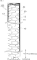
- FIG. 1 is a plan view showing a structure of a light emitting device 100.
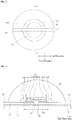
- FIG. 2 is an enlarged plan view near a light emitting element 30 shown in FIG. 1 .
- FIG. 3 is a cross sectional view taken along line A-A of FIG. 2 .
- the light emitting device 100 includes a substrate member 10, a plurality of sealing members 20, and a plurality of light emitting elements 30.
- the light emitting device 100 is flexible, so that it can be stored rolled-up on a reel etc., and can be installed along a curved surface.
- the substrate member 10 of is an elongated member.
- the first direction corresponds to the longitudinal direction of the substrate member 10 and the second direction which is substantially perpendicular to the first direction corresponds to the lateral direction of the substrate member 10.
- the ratio of the lengths of the substrate member 10 in the longitudinal direction and the lateral direction can be appropriately adjusted, for example, to be 6:1, 30:1, or 100:1.
- the length of the substrate member 10 in the first direction can be, for example, 1150 mm
- the length of the substrate member 10 in the second direction can be, for example, 15 mm.
- the substrate member 10 includes a flexible base member 11, at least one wiring portion 12, at least one wiring portion 13, a groove portion 14 defined between ones of the wiring portion 12 and wiring portion 13 which are adjacent and spaced apart from each other, a reflecting layer 15, and an adhesive agent 16 which connects the base member 11 and the wiring portions 12, 13.
- the base member 11 is made of a flexible insulating material.
- an insulating resin such as polyimide (PI), polyethylene naphthalate (PEN), and polyethylene terephthalate (PET) can be preferably used but is not limited thereto.
- the base member 11 may be made of a strip of copper foil or aluminum foil which is covered with an insulating resin.
- the base member 11 can have a thickness of about 10 ⁇ m to about 100 ⁇ m, for example.
- the material of the base member 11 can be appropriately selected in view of the type of mounting of the light emitting elements 30, the reflectance, and adhesion with other members, etc.
- a polyimide which has a high heat resisting property is preferably used, and in the case where the reflecting layer 15 which to be described below is not disposed on the substrate 11, a material which has a high optical reflectance (for example a white color material) is preferably used so that a light emitting device with good light extraction efficiency can be obtained.
- a material which has a high optical reflectance for example a white color material
- the substrate member 11 may be particularly prone to deterioration due to light, and thus, the effects of the present invention can be exhibited effectively.
- the wiring portions 12 and 13 are arranged on a main surface of the base member 11.
- the wiring portions 12 and 13 are arranged spaced apart from each other. With this arrangement, the groove portion 14 to be described below is defined between the wiring portions 12 and 13.
- the wiring portions 12 and 13 as described above are made of a thin metal film such as a copper foil or an aluminum foil, for example.
- the wiring portions 12 and 13 have a thickness which does not impair the flexibility of the substrate member 10 and a thickness of 8 ⁇ m to 150 ⁇ m is preferable.
- the wiring portions 12 and 13 are preferably arranged on the base member 11 respectively with a largest possible area. An increase in the surface area of the wiring portions 12 and 13 allows for increased heat dissipation from the wiring portions 12 and 13.
- the corners of the wiring portions 12 and 13 in a plan view are preferably rounded for improving the adhesion (anti-detachment feature) of the wiring portions, which can enhance the reliability.
- the corners are preferably rounded with a radius of 100 ⁇ m or more.
- the groove portion 14 is defined between the wiring portions 12 and 13 which are spaced apart from each other, so that the shape of the groove portion is in conformity to the shapes of the wiring portions, which may be, for example, a crank shape.
- the width defining the groove portions 14 is preferably narrower than the width of the wiring portions 12 and 13, and, for example, can be about 0.05 mm to about 5 mm.
- the plurality of wiring portions 12, 13 are spaced apart from each other and the separation creates the groove portion where the wiring portions are not disposed (i.e., the portion where the base member and the adhesion layer are not covered with the wiring portions).
- the wiring portions 12 and 13 are respectively arranged on the base member 11 via the adhesive agent 16.
- the adhesive agent is made of a resin such as an epoxy-based resin, an imide-based resin, an amide-based resin, an acrylic-based resin, a silicone-based resin.
- the adhesive agent 16 preferably has a thickness of 1 ⁇ m to 50 ⁇ m.
- the adhesive agent 16 is configured to adhere the wiring portions 12, 13 and the base member 11 respectively, and is applied not only between the wiring portions and the base member, but also is extended to cover the groove portion 14 which is a region where the wiring portions 12, 13 are not arranged.
- a light-shielding member in the adhesive agent 16 so that light, which is of at least a specific wavelength, emitted from the light emitting elements 30 can be absorbed or shielded by the light-shielding member. That is, inclusion of a light-shielding member, which can shield a part or all of the light from the light emitting elements 30, in the adhesive agent 16 allows for shielding the light irradiated on the base member 11. Thus, deterioration of the base member 11 due to light can be reduced.
- the polyimide substrate member is exposed in a region which does not have the electrically conductive region, and irradiation of light from the light emitting element on the exposed region may result in deterioration of the polyimide.
- a flexible substrate member such as a polyimide substrate member with a small thickness of about several tens of micrometers
- deterioration of the exposed region which has to be formed near the light emitting element poses a problem.
- Deterioration of the polyimide substrate member due to discoloration and/or degradation of strength may adversely affect the withstand voltage.
- the present embodiment can provide a light emitting device in which degradation of the substrate member can be reduced.
- the light-shielding member is preferably at least one selected from the group consisting of a light-absorption materials, wavelength converting materials, and light-reflecting materials. More specific examples of the light-absorption materials include carbon black, pigments, and colorants.
- the light-reflecting material is to exhibit light-diffusing effect by employing a difference in the refractive index with the adhesive material, and for example, a while filler such as SiO 2 , TiO 2 , Al 2 O 3 , ZrO 2 , MgO, or BaSO 4 ; or pores of submicron sizes can be used. Also, interference or a mirror material with the use of a metal layer can be used.
- the wavelength converting material is to absorb light, which is of at least a specific wavelength, emitted from the light emitting elements 30 and to convert the absorbed light to light of a different wavelength.
- the wavelength converting material is to convert the emission wavelength of the light emitting elements 30 into a wavelength which hardly degrade the base member 11. More specifically, an oxide-based fluorescent material, a nitride-based fluorescent material, and/or a sulfide-based material can be preferably used as the wavelength converting material.
- the size and shape of the light-shading member are not specifically limited.
- a spherical shape, a scale-like shape, or a needle-like shape with a size of 1 nm to 50 ⁇ m can be used.
- two or more materials as described above can be used in combination.
- the light from the light emitting elements can be diffused by the light-reflecting material to increase the optical path length which can increase the probability of light to hit the light-absorption material.
- the usage amount of the light-absorption material can be reduced.
- Carbon black which can be suitably used as the light-absorption material has electrical conductivity. So that a reduction in the use of carbon black can increase electrical insulation and thus preferable.
- the adhesive agent 16 preferably contains the light-shielding member in a range of 0.01 to 60 weight % with respect to the weight of the adhesive agent 16. More specifically, for example, 0.005 to 10 weight %, preferably 0.01 to 5 weight % of the light-absorption material, 1 to 50 weight %, preferably 2 to 40 weight % of the wavelength converting material, and/or 1 to 100 weight %, preferably 2.5 to 50 weight % of the light-reflecting material may be employed.
- the adhesive agent 16 preferably has a lower light transmissive rate than the resin layer 106 to be described below, to the light from the light emitting elements 30. With this arrangement, light which is transmitting through the resin layer 106 can be shielded.
- the reflective layer 15 covers the surfaces of the base member 11 and the wiring portions 12, 13.
- the reflective layer 15 also covers the groove portion 14.
- the reflective layer 15 covers approximately the entire upper surface of the substrate 10 except for the opening portions 15S to be described below.
- Such a reflective layer 15 is made of a material which can reflect the emitted light (including the wavelength-converted light by a wavelength converting member) from the at least one light emitting element 30.
- an insulating white ink which is referred to as "a white resist” made of a silicone resin containing titanium oxide is preferably used but is not limited thereto.
- openings 15S are defined in the reflecting layer 15 at least in and around the regions where the light emitting elements 30 to be arranged respectively.
- FIG. 2 and FIG. 3 show one of the openings 15S formed over the two wiring portions 12 and 13. As shown in FIG. 2 and FIG. 3 , in the opening 15S, the two wiring portions 12 and 13 and the groove portion 14 are partially exposed.
- the openings 15S can be formed in an appropriate shape such as a circular shape or a quadrangular shape adapted to surround the light emitting elements 30 in a plan view, respectively.
- the openings 15S are preferably covered with a resin layer 106 (an underfill material), a sealing member 20, and/or other appropriate light-reflecting member.
- a resin layer 106 an underfill material
- a sealing member 20 an underfill material
- other appropriate light-reflecting member With this arrangement, each of the portion around the respective light emitting elements 30 can be protected.
- the use of a material having a higher optical reflectance than that of the substrate member 10 and the wiring portions 12 and 13 which are exposed in the each opening 15S for the covering can improve the light extraction efficiency of the light emitting device.
- the reflecting layer 15 may be disposed extending below the light emitting elements 30 with the openings 15S smaller than the shape in a plan view of the light emitting elements 30.
- the reflecting layer 15 may be disposed to surround the bonding member of each light emitting element, so that the opening is not substantially formed. In this case, the light extraction efficiency of the light emitting device can be enhanced without using a material such as an underfill material to be described below.
- the groove portion 14 is entirely covered with the reflecting layer 15, the light from the light emitting elements 30 can be prevented from irradiating on the base member 11. But a certain amount of light is supposed to be transmitted depending on the thickness of the reflecting layer 15. Thus, even in the case where the groove portion 14 is completely covered with the reflecting layer 15, disposing of a light-shielding member allows for shielding of light which transmits through the reflecting layer 15.
- the wiring portions 12, 13 also serve as the terminal portions which are connected to external wirings to be connected to an external power source.
- the terminal portions are preferably formed at an end portion at the main surface-side of the base member 11, and the external wirings may be connected to publicly known connectors disposed on the substrate member 10.
- sealing members 20 are arranged on the substrate member 10.
- the sealing members 20 are disposed so as to respectively enclose the openings 15S defined in the reflecting layer 15.
- Each of the sealing members 20 seals one light emitting element 30.
- the sealing members 20 are, as shown in FIG. 3 , respectively formed in a hemisphere shape with one light emitting element 30 at the center, but is not limited thereto, and may be formed in an appropriate shape such as a rectangular parallelepiped shape or a semicylindrical shape.
- Such sealing members 20 are made up of a light transmissive resin (for example, an epoxy resin, a urea resin, a silicone resin, etc.).
- the sealing members 20 may contain a light-scattering agent (barium sulfate, titanium oxide, aluminum oxide, silicon oxide, etc.).
- the material of the sealing members 20 is not limited to a resin material such as described above, and a light transmissive glass or the like may be employed.
- the sealing members 20 preferably contain a wavelength converting member which can absorb emission from the light emitting elements 30 and emits light of a different wavelength. With this arrangement, a light emitting device to emit light of a desired color can be obtained.
- a wavelength converting member include an oxide-based fluorescent material, a sulfide-based fluorescent material, and a nitride-based fluorescent material.
- a fluorescent material to absorb blue light such as a YAG-based fluorescent material or a LAG-based fluorescent material to emit yellow to green light, a SiAION-based fluorescent material to emit green light, and a SCASN-based fluorescent material and a CASN-based fluorescent material to emit red light, are preferably used singly or in combination.
- a light emitting device to emit white light can be obtained.
- a SiAION-based fluorescent material and a SCASN-based fluorescent material are preferably used singly or in combination. With this arrangement, a light emitting device having high color reproductivity can be obtained. Also, in a light emitting device for lighting applications, a YAG-based fluorescent material or a LAG-based fluorescent material and a SCASN-based fluorescent material or a CASN-based fluorescent material are preferably used in combination. With this arrangement, a light emitting device having high color rendering properties can be realized.
- the use of the wavelength converting member as described above is not limited to be contained in the sealing member 20, but can be used external of the light emitting device 100, for example, disposed in a display device or a lighting device which uses the light emitting device 100 as its light source.
- the at least one light emitting element 30 is disposed on the substrate member 10.
- the light emitting elements 30 are respectively disposed in the openings 15S formed in the reflective layer 15.
- the light emitting elements 30 are respectively connected to the wiring portions 12 and 13.
- each light emitting element 30 is arranged so as to straddle at least a part of the groove portion 14, and the longitudinal direction of each light emitting element 30 can be substantially in parallel with the second direction.
- each of the light emitting elements 30 is, as shown in FIG. 3 , mounted on the substrate member 10 in a flip-chip manner.
- Each light emitting element 30 is connected to the wiring portions 12, 13 via a pair of bonding members 105 respectively.
- the bonding member 105 can be made of, for example, a solder such as Sn-Ag-Cu system, Au-Sn system, or a Sn-Cu system, a metal such as Au, an anisotropic conductive paste, or an Ag paste.
- a resin layer 106 (an underfill material) is filled between the light emitting element 30 and the base member 11.
- the resin layer 106 is, as shown in FIG. 3 , preferably disposed not only on the wiring portions 12, 13 but also on the reflecting layer 15.
- the resin layer 106 can be made of, for example, a silicone resin or an epoxy resin, a fluororesin, or a hybrid resin containing one or more those resins.
- the resin layer 106 preferably has a light reflecting property by containing a material having a white color such as titanium oxide, silicon oxide, or alumina. With this arrangement, the light extraction efficiency of the light emitting elements can be increased. Also in this case the resin layer 106 is supposed to allow a certain amount of light to transmit therethrough, so that providing the light-shielding member allows for shielding of light which is transmitting through the resin layer 106.
- the light emitting elements 30 respectively include a semiconductor structure 31, a p-side electrode 32, an n-side electrode 33, and an insulating layer 34, as shown in FIG. 3 .
- the semiconductor structure 31 includes an n-type layer, an active layer, and a p-type layer which are stacked in the order on a light-transmissive sapphire substrate.
- the n-type layer, the active layer and the p-type layers can be respectively made of, for example, a gallium nitride-based semiconductor.
- the p-side electrode 32 and the n-side electrode 33 are respectively connected to a pair of wiring portions 12 and 13 via a pair of bonding members 105.
- the n-side electrode 33 is extended to a lower portion of the p-type layer via the insulating material layer 34.
- the p-side electrode 32 and the n-side electrode 33 are disposed so that the portions facing each other can be in parallel with each other. This arrangement facilitates disposition (mounting) over the groove portion 14.
- the p-side electrode 32 and the n-side electrode 33 preferably have approximately same size and shape. With this arrangement, the stress experienced on the light emitting elements 30 caused by bending of the substrate member 10 can be dispersed, so that malfunction of the light emitting elements 30 can be reduced.
- the light emitting device 100 as described above employs the flexible substrate member 10, so that a roll-to-roll processing method can be used for manufacturing.
- the base member 11 and the wiring portions 12 and 13 are adhered with an adhesive agent 16, using a polyimide sheet with a thickness of 25 ⁇ m for the base member 11 and Cu with a thickness of 35 ⁇ m for the wiring portions 12 and 13.
- an adhesive agent 16 using a polyimide sheet with a thickness of 25 ⁇ m for the base member 11 and Cu with a thickness of 35 ⁇ m for the wiring portions 12 and 13.
- the sheet With the use of a thermosetting epoxy-based adhesive material which contains 3 wt% of carbon black as a light-shielding member, the sheet is formed with a thickness of about 10 ⁇ m.
- a resin layer 106 is formed around the light emitting elements 30 with applying an underfill material of a silicone resin which includes a 30 wt% of titanium oxide having an average diameter of 0.25 ⁇ m.
- a silicone resin is disposed in a dome shape as the sealing member 20.
- the light emitting device fabricated as described above can reduce the amount of light irradiated on the polyimide sheet and allows little light to leak to the backside of the base member 10.
- the wavelength of light that causes decomposition of C-N bonding portions in the imide groups which are included in the polyimide is 448.9 nm. Thus, in the case where employing a light emitting element with the emission wavelength of about 450 nm.
Landscapes
- Engineering & Computer Science (AREA)
- Microelectronics & Electronic Packaging (AREA)
- Led Device Packages (AREA)
Claims (13)
- Dispositif électroluminescent (100) comprenant :un élément base (11) comprenant une résine ;une pluralité de parties câblages (12, 13) ;une partie rainure (14) définie entre des parties câblages adjacentes (12, 13) ; etau moins un élément électroluminescent (30) disposé de façon à enjamber une partie au moins de la partie rainure (14),caractérisé en ce que :la pluralité de parties câblages (12, 13) sont collées sur l'élément base (11) avec un agent adhésif (16) configuré pour coller les parties câblages (12,13) et l'élément base (11);l'agent adhésif (16) comprend un élément de protection vis-à-vis de la lumière, disposé entre les parties câblages (12, 13) et l'élément base (11), et qui s'étend afin de couvrir la partie rainure (14) qui est une région où les parties câblages (12, 13) ne sont pas agencées ; etl'élément de protection vis-à-vis de la lumière est configuré afin de protéger l'élément base (11) vis-à-vis d'une longueur d'onde spécifique au moins de la lumière émise par l'élément électroluminescent (30).
- Dispositif électroluminescent (100) selon la revendication 1, où :
l'élément de protection vis-à-vis de la lumière est configuré afin de protéger l'élément base (11) vis-à-vis de la lumière émise par l'élément électroluminescent (30). - Dispositif électroluminescent (100) selon la revendication 1 ou 2, où :
l'élément base (11) est souple. - Dispositif électroluminescent (100) selon l'une quelconque des revendications 1 à 3, où :
l'élément de protection vis-à-vis de la lumière est l'un au moins d'un matériau d'absorption de la lumière, d'un matériau de conversion d'une longueur d'onde, et d'un matériau de réflexion de la lumière. - Dispositif électroluminescent (100) selon l'une quelconque des revendications 1 à 4, comprenant en outre :une couche réfléchissante disposée afin de couvrir une partie de chacune des parties câblages (12, 13), et comprenant une pluralité d'ouvertures ;les ouvertures définies correspondant au moins aux emplacements du ou des éléments électroluminescents (30), et étant agencées pour exposer des parties des parties câblages (12, 13) et des parties rainures (14).
- Dispositif électroluminescent (100) selon la revendication 5, comprenant en outre :une couche de résine agencée dans chaque ouverture et autour de l'élément électroluminescent (30) ; etl'agent adhésif (16) présentant une transmittance optique inférieure à celle de la couche de résine vis-à-vis de la lumière en provenance de l'élément électroluminescent (30).
- Dispositif électroluminescent (100) selon l'une quelconque des revendications 1 à 6, où:
l'élément base (11) comprend l'un au moins d'un polyimide (PI), d'un polyéthylène naphthalate (PEN), et d'un polyéthylène téréphtalate (PET). - Dispositif électroluminescent (100) selon l'une quelconque des revendications 1 à 7, où :
l'élément de protection vis-à-vis de la lumière est du noir de carbone. - Dispositif électroluminescent (100) selon l'une quelconque des revendications 1 à 8, où :
l'élément de protection vis-à-vis de la lumière comprend un matériau d'absorption de la lumière et un matériau de réflexion de la lumière. - Dispositif électroluminescent (100) selon l'une quelconque des revendications 1 à 9, où :
l'élément de protection vis-à-vis de la lumière est configuré en outre pour absorber la lumière émise par l'élément électroluminescent (30), et pour émettre une lumière d'une longueur d'onde différente. - Dispositif électroluminescent (100) selon l'une quelconque des revendications 1 à 10, comprenant en outre :
une pluralité de parties rainures (14) définies entre des parties câblages adjacentes (12, 13). - Dispositif électroluminescent (100) selon l'une quelconque des revendications 1 à 11, où :
l'agent adhésif (16) couvre l'élément base (11). - Dispositif électroluminescent (100) selon l'une quelconque des revendications 1 à 12, où :
l'agent adhésif est constitué de résine.
Applications Claiming Priority (1)
| Application Number | Priority Date | Filing Date | Title |
|---|---|---|---|
| JP2013137693A JP6255747B2 (ja) | 2013-07-01 | 2013-07-01 | 発光装置 |
Publications (2)
| Publication Number | Publication Date |
|---|---|
| EP2822046A1 EP2822046A1 (fr) | 2015-01-07 |
| EP2822046B1 true EP2822046B1 (fr) | 2019-08-14 |
Family
ID=50982843
Family Applications (1)
| Application Number | Title | Priority Date | Filing Date |
|---|---|---|---|
| EP14174704.8A Active EP2822046B1 (fr) | 2013-07-01 | 2014-06-27 | Dispositif électroluminescent |
Country Status (4)
| Country | Link |
|---|---|
| US (1) | US9231177B2 (fr) |
| EP (1) | EP2822046B1 (fr) |
| JP (1) | JP6255747B2 (fr) |
| CN (1) | CN104282822B (fr) |
Families Citing this family (18)
| Publication number | Priority date | Publication date | Assignee | Title |
|---|---|---|---|---|
| KR20160087048A (ko) * | 2015-01-12 | 2016-07-21 | 삼성전자주식회사 | 발광다이오드 패키지 |
| JP6543998B2 (ja) * | 2015-03-30 | 2019-07-17 | 大日本印刷株式会社 | Ledバックライト及びそれを用いたled表示装置 |
| JP6558034B2 (ja) * | 2015-04-03 | 2019-08-14 | 大日本印刷株式会社 | Led素子用のフレキシブル多層回路基板及びそれを用いたledドットマトリックス表示装置 |
| JP6572083B2 (ja) * | 2015-09-30 | 2019-09-04 | 大日本印刷株式会社 | 発光素子用基板、モジュール及び発光素子用基板の製造方法 |
| JP6918452B2 (ja) * | 2015-09-30 | 2021-08-11 | 大日本印刷株式会社 | 発光素子用基板及びモジュール |
| JP6556009B2 (ja) * | 2015-09-30 | 2019-08-07 | 大日本印刷株式会社 | 発光素子用基板、モジュール及び発光素子用基板の製造方法 |
| US10199545B2 (en) | 2015-09-30 | 2019-02-05 | Dai Nippon Printing Co., Ltd. | Substrate for light emitting element and module |
| JP6451579B2 (ja) | 2015-09-30 | 2019-01-16 | 日亜化学工業株式会社 | 発光装置 |
| WO2017061127A1 (fr) | 2015-10-08 | 2017-04-13 | Nichia Corporation | Dispositif émetteur de lumière, dispositif émetteur de lumière intégré et module émetteur de lumière |
| JP6524904B2 (ja) | 2015-12-22 | 2019-06-05 | 日亜化学工業株式会社 | 発光装置 |
| JP6776855B2 (ja) | 2016-12-06 | 2020-10-28 | 日亜化学工業株式会社 | 発光装置 |
| JP6868388B2 (ja) | 2016-12-26 | 2021-05-12 | 日亜化学工業株式会社 | 発光装置および集積型発光装置 |
| JP7277815B2 (ja) * | 2017-06-13 | 2023-05-19 | 日亜化学工業株式会社 | 発光装置の製造方法および発光装置 |
| KR102473399B1 (ko) * | 2017-06-26 | 2022-12-02 | 쑤저우 레킨 세미컨덕터 컴퍼니 리미티드 | 발광소자 패키지 및 광원 장치 |
| KR102401826B1 (ko) * | 2017-09-15 | 2022-05-25 | 쑤저우 레킨 세미컨덕터 컴퍼니 리미티드 | 발광소자 패키지 및 이를 포함하는 조명장치 |
| JP7064127B2 (ja) | 2017-09-29 | 2022-05-10 | 日亜化学工業株式会社 | 発光装置およびその製造方法 |
| US11594662B2 (en) * | 2019-07-31 | 2023-02-28 | Nichia Corporation | Light-emitting device |
| JP7021447B2 (ja) | 2020-10-05 | 2022-02-17 | 日亜化学工業株式会社 | 発光装置 |
Family Cites Families (23)
| Publication number | Priority date | Publication date | Assignee | Title |
|---|---|---|---|---|
| JP3864862B2 (ja) * | 2002-04-04 | 2007-01-10 | セイコーエプソン株式会社 | 電気光学装置及び電子機器 |
| WO2004081140A1 (fr) * | 2003-03-13 | 2004-09-23 | Nichia Corporation | Film luminescent, dispositif luminescent, procede de fabrication d'un film luminescent, et procede de fabrication d'un dispositif luminescent |
| JP4505794B2 (ja) * | 2004-03-10 | 2010-07-21 | 信越半導体株式会社 | 発光素子の製造方法 |
| US20050247944A1 (en) * | 2004-05-05 | 2005-11-10 | Haque Ashim S | Semiconductor light emitting device with flexible substrate |
| KR100624307B1 (ko) * | 2005-02-23 | 2006-09-19 | 제일모직주식회사 | 표시장치용 저반사율의 휘도 향상 다층 광학필름 및 이를이용한 유기발광다이오드 표시장치 |
| JP4049186B2 (ja) * | 2006-01-26 | 2008-02-20 | ソニー株式会社 | 光源装置 |
| CN101379344B (zh) | 2006-01-31 | 2013-08-28 | 3M创新有限公司 | 具有适形箔结构的led照明组件 |
| US20070285740A1 (en) * | 2006-05-02 | 2007-12-13 | Rohm Co., Ltd. | Image sensor module |
| US7806560B2 (en) | 2007-01-31 | 2010-10-05 | 3M Innovative Properties Company | LED illumination assembly with compliant foil construction |
| JP4107349B2 (ja) | 2007-06-20 | 2008-06-25 | ソニー株式会社 | 光源装置、表示装置 |
| JP2010109119A (ja) | 2008-10-30 | 2010-05-13 | Sanyo Electric Co Ltd | 発光モジュール及びその製造方法 |
| US8704258B2 (en) * | 2009-06-26 | 2014-04-22 | Asahi Rubber Inc. | White color reflecting material and process for production thereof |
| JP5996871B2 (ja) * | 2010-02-09 | 2016-09-21 | 日亜化学工業株式会社 | 発光装置および発光装置の製造方法 |
| JP2011233650A (ja) | 2010-04-26 | 2011-11-17 | Toshiba Corp | 半導体発光装置 |
| JP2012044102A (ja) * | 2010-08-23 | 2012-03-01 | Hitachi Cable Ltd | 発光装置及びその製造方法並びに配線基板 |
| JP5772007B2 (ja) * | 2011-01-24 | 2015-09-02 | 日亜化学工業株式会社 | 発光装置及び発光装置の製造方法 |
| JP5582048B2 (ja) * | 2011-01-28 | 2014-09-03 | 日亜化学工業株式会社 | 発光装置 |
| JP5797945B2 (ja) * | 2011-06-21 | 2015-10-21 | シチズン電子株式会社 | Ledランプ |
| JP5985846B2 (ja) * | 2011-06-29 | 2016-09-06 | Flexceed株式会社 | 発光素子搭載用基板及びledパッケージ |
| JP2013084803A (ja) | 2011-10-11 | 2013-05-09 | Hitachi Cable Ltd | 発光装置、発光素子パッケージ及び発光素子搭載用配線基板 |
| JP2013110154A (ja) * | 2011-11-17 | 2013-06-06 | Sanken Electric Co Ltd | 発光装置 |
| JP2013135069A (ja) * | 2011-12-26 | 2013-07-08 | Hitachi Cable Ltd | 発光素子搭載用配線基板、発光モジュール及び発光素子搭載用配線基板の製造方法 |
| US9627572B2 (en) * | 2012-04-25 | 2017-04-18 | Kyocera Corporation | Light receiving and emitting element module and sensor device using same |
-
2013
- 2013-07-01 JP JP2013137693A patent/JP6255747B2/ja active Active
-
2014
- 2014-06-27 US US14/317,008 patent/US9231177B2/en active Active
- 2014-06-27 EP EP14174704.8A patent/EP2822046B1/fr active Active
- 2014-07-01 CN CN201410309412.3A patent/CN104282822B/zh active Active
Non-Patent Citations (1)
| Title |
|---|
| None * |
Also Published As
| Publication number | Publication date |
|---|---|
| CN104282822A (zh) | 2015-01-14 |
| US20150001564A1 (en) | 2015-01-01 |
| JP2015012206A (ja) | 2015-01-19 |
| JP6255747B2 (ja) | 2018-01-10 |
| EP2822046A1 (fr) | 2015-01-07 |
| US9231177B2 (en) | 2016-01-05 |
| CN104282822B (zh) | 2018-09-11 |
Similar Documents
| Publication | Publication Date | Title |
|---|---|---|
| EP2822046B1 (fr) | Dispositif électroluminescent | |
| KR102218518B1 (ko) | 발광 장치 | |
| US10396058B2 (en) | Light-emitting device | |
| US9279571B2 (en) | Light emitting device | |
| KR101762324B1 (ko) | 발광 소자 | |
| US9366393B2 (en) | Light emitting device | |
| US11171261B2 (en) | Light emitting device | |
| KR102227769B1 (ko) | 반도체 발광소자 및 이를 이용한 반도체 발광소자 패키지 | |
| US9388951B2 (en) | Stacked assembly of light emitting devices | |
| WO2016093325A1 (fr) | Dispositif électroluminescent | |
| KR101163861B1 (ko) | 발광소자, 전극 구조 및 발광 소자 패키지 | |
| JP6343923B2 (ja) | 発光装置 | |
| JP2014082481A (ja) | 発光装置 | |
| US9385283B2 (en) | Light emitting device equipped with protective member | |
| JP6135199B2 (ja) | 発光装置 | |
| KR102426873B1 (ko) | 발광 소자 패키지 | |
| CN117832359A (zh) | 一种发光装置及显示装置 |
Legal Events
| Date | Code | Title | Description |
|---|---|---|---|
| PUAI | Public reference made under article 153(3) epc to a published international application that has entered the european phase |
Free format text: ORIGINAL CODE: 0009012 |
|
| 17P | Request for examination filed |
Effective date: 20140627 |
|
| AK | Designated contracting states |
Kind code of ref document: A1 Designated state(s): AL AT BE BG CH CY CZ DE DK EE ES FI FR GB GR HR HU IE IS IT LI LT LU LV MC MK MT NL NO PL PT RO RS SE SI SK SM TR |
|
| AX | Request for extension of the european patent |
Extension state: BA ME |
|
| R17P | Request for examination filed (corrected) |
Effective date: 20150707 |
|
| RBV | Designated contracting states (corrected) |
Designated state(s): AL AT BE BG CH CY CZ DE DK EE ES FI FR GB GR HR HU IE IS IT LI LT LU LV MC MK MT NL NO PL PT RO RS SE SI SK SM TR |
|
| STAA | Information on the status of an ep patent application or granted ep patent |
Free format text: STATUS: EXAMINATION IS IN PROGRESS |
|
| 17Q | First examination report despatched |
Effective date: 20180103 |
|
| GRAP | Despatch of communication of intention to grant a patent |
Free format text: ORIGINAL CODE: EPIDOSNIGR1 |
|
| STAA | Information on the status of an ep patent application or granted ep patent |
Free format text: STATUS: GRANT OF PATENT IS INTENDED |
|
| INTG | Intention to grant announced |
Effective date: 20190312 |
|
| GRAS | Grant fee paid |
Free format text: ORIGINAL CODE: EPIDOSNIGR3 |
|
| GRAA | (expected) grant |
Free format text: ORIGINAL CODE: 0009210 |
|
| STAA | Information on the status of an ep patent application or granted ep patent |
Free format text: STATUS: THE PATENT HAS BEEN GRANTED |
|
| AK | Designated contracting states |
Kind code of ref document: B1 Designated state(s): AL AT BE BG CH CY CZ DE DK EE ES FI FR GB GR HR HU IE IS IT LI LT LU LV MC MK MT NL NO PL PT RO RS SE SI SK SM TR |
|
| REG | Reference to a national code |
Ref country code: GB Ref legal event code: FG4D |
|
| REG | Reference to a national code |
Ref country code: CH Ref legal event code: EP Ref country code: AT Ref legal event code: REF Ref document number: 1168063 Country of ref document: AT Kind code of ref document: T Effective date: 20190815 |
|
| REG | Reference to a national code |
Ref country code: DE Ref legal event code: R096 Ref document number: 602014051651 Country of ref document: DE |
|
| REG | Reference to a national code |
Ref country code: IE Ref legal event code: FG4D |
|
| REG | Reference to a national code |
Ref country code: NL Ref legal event code: MP Effective date: 20190814 |
|
| REG | Reference to a national code |
Ref country code: LT Ref legal event code: MG4D |
|
| PG25 | Lapsed in a contracting state [announced via postgrant information from national office to epo] |
Ref country code: PT Free format text: LAPSE BECAUSE OF FAILURE TO SUBMIT A TRANSLATION OF THE DESCRIPTION OR TO PAY THE FEE WITHIN THE PRESCRIBED TIME-LIMIT Effective date: 20191216 Ref country code: BG Free format text: LAPSE BECAUSE OF FAILURE TO SUBMIT A TRANSLATION OF THE DESCRIPTION OR TO PAY THE FEE WITHIN THE PRESCRIBED TIME-LIMIT Effective date: 20191114 Ref country code: NL Free format text: LAPSE BECAUSE OF FAILURE TO SUBMIT A TRANSLATION OF THE DESCRIPTION OR TO PAY THE FEE WITHIN THE PRESCRIBED TIME-LIMIT Effective date: 20190814 Ref country code: HR Free format text: LAPSE BECAUSE OF FAILURE TO SUBMIT A TRANSLATION OF THE DESCRIPTION OR TO PAY THE FEE WITHIN THE PRESCRIBED TIME-LIMIT Effective date: 20190814 Ref country code: LT Free format text: LAPSE BECAUSE OF FAILURE TO SUBMIT A TRANSLATION OF THE DESCRIPTION OR TO PAY THE FEE WITHIN THE PRESCRIBED TIME-LIMIT Effective date: 20190814 Ref country code: NO Free format text: LAPSE BECAUSE OF FAILURE TO SUBMIT A TRANSLATION OF THE DESCRIPTION OR TO PAY THE FEE WITHIN THE PRESCRIBED TIME-LIMIT Effective date: 20191114 Ref country code: FI Free format text: LAPSE BECAUSE OF FAILURE TO SUBMIT A TRANSLATION OF THE DESCRIPTION OR TO PAY THE FEE WITHIN THE PRESCRIBED TIME-LIMIT Effective date: 20190814 Ref country code: SE Free format text: LAPSE BECAUSE OF FAILURE TO SUBMIT A TRANSLATION OF THE DESCRIPTION OR TO PAY THE FEE WITHIN THE PRESCRIBED TIME-LIMIT Effective date: 20190814 |
|
| REG | Reference to a national code |
Ref country code: AT Ref legal event code: MK05 Ref document number: 1168063 Country of ref document: AT Kind code of ref document: T Effective date: 20190814 |
|
| PG25 | Lapsed in a contracting state [announced via postgrant information from national office to epo] |
Ref country code: IS Free format text: LAPSE BECAUSE OF FAILURE TO SUBMIT A TRANSLATION OF THE DESCRIPTION OR TO PAY THE FEE WITHIN THE PRESCRIBED TIME-LIMIT Effective date: 20191214 Ref country code: RS Free format text: LAPSE BECAUSE OF FAILURE TO SUBMIT A TRANSLATION OF THE DESCRIPTION OR TO PAY THE FEE WITHIN THE PRESCRIBED TIME-LIMIT Effective date: 20190814 Ref country code: GR Free format text: LAPSE BECAUSE OF FAILURE TO SUBMIT A TRANSLATION OF THE DESCRIPTION OR TO PAY THE FEE WITHIN THE PRESCRIBED TIME-LIMIT Effective date: 20191115 Ref country code: ES Free format text: LAPSE BECAUSE OF FAILURE TO SUBMIT A TRANSLATION OF THE DESCRIPTION OR TO PAY THE FEE WITHIN THE PRESCRIBED TIME-LIMIT Effective date: 20190814 Ref country code: AL Free format text: LAPSE BECAUSE OF FAILURE TO SUBMIT A TRANSLATION OF THE DESCRIPTION OR TO PAY THE FEE WITHIN THE PRESCRIBED TIME-LIMIT Effective date: 20190814 Ref country code: LV Free format text: LAPSE BECAUSE OF FAILURE TO SUBMIT A TRANSLATION OF THE DESCRIPTION OR TO PAY THE FEE WITHIN THE PRESCRIBED TIME-LIMIT Effective date: 20190814 |
|
| PG25 | Lapsed in a contracting state [announced via postgrant information from national office to epo] |
Ref country code: TR Free format text: LAPSE BECAUSE OF FAILURE TO SUBMIT A TRANSLATION OF THE DESCRIPTION OR TO PAY THE FEE WITHIN THE PRESCRIBED TIME-LIMIT Effective date: 20190814 |
|
| PG25 | Lapsed in a contracting state [announced via postgrant information from national office to epo] |
Ref country code: IT Free format text: LAPSE BECAUSE OF FAILURE TO SUBMIT A TRANSLATION OF THE DESCRIPTION OR TO PAY THE FEE WITHIN THE PRESCRIBED TIME-LIMIT Effective date: 20190814 Ref country code: RO Free format text: LAPSE BECAUSE OF FAILURE TO SUBMIT A TRANSLATION OF THE DESCRIPTION OR TO PAY THE FEE WITHIN THE PRESCRIBED TIME-LIMIT Effective date: 20190814 Ref country code: EE Free format text: LAPSE BECAUSE OF FAILURE TO SUBMIT A TRANSLATION OF THE DESCRIPTION OR TO PAY THE FEE WITHIN THE PRESCRIBED TIME-LIMIT Effective date: 20190814 Ref country code: DK Free format text: LAPSE BECAUSE OF FAILURE TO SUBMIT A TRANSLATION OF THE DESCRIPTION OR TO PAY THE FEE WITHIN THE PRESCRIBED TIME-LIMIT Effective date: 20190814 Ref country code: AT Free format text: LAPSE BECAUSE OF FAILURE TO SUBMIT A TRANSLATION OF THE DESCRIPTION OR TO PAY THE FEE WITHIN THE PRESCRIBED TIME-LIMIT Effective date: 20190814 Ref country code: PL Free format text: LAPSE BECAUSE OF FAILURE TO SUBMIT A TRANSLATION OF THE DESCRIPTION OR TO PAY THE FEE WITHIN THE PRESCRIBED TIME-LIMIT Effective date: 20190814 |
|
| PG25 | Lapsed in a contracting state [announced via postgrant information from national office to epo] |
Ref country code: CZ Free format text: LAPSE BECAUSE OF FAILURE TO SUBMIT A TRANSLATION OF THE DESCRIPTION OR TO PAY THE FEE WITHIN THE PRESCRIBED TIME-LIMIT Effective date: 20190814 Ref country code: SK Free format text: LAPSE BECAUSE OF FAILURE TO SUBMIT A TRANSLATION OF THE DESCRIPTION OR TO PAY THE FEE WITHIN THE PRESCRIBED TIME-LIMIT Effective date: 20190814 Ref country code: IS Free format text: LAPSE BECAUSE OF FAILURE TO SUBMIT A TRANSLATION OF THE DESCRIPTION OR TO PAY THE FEE WITHIN THE PRESCRIBED TIME-LIMIT Effective date: 20200224 Ref country code: SM Free format text: LAPSE BECAUSE OF FAILURE TO SUBMIT A TRANSLATION OF THE DESCRIPTION OR TO PAY THE FEE WITHIN THE PRESCRIBED TIME-LIMIT Effective date: 20190814 |
|
| REG | Reference to a national code |
Ref country code: DE Ref legal event code: R097 Ref document number: 602014051651 Country of ref document: DE |
|
| PLBE | No opposition filed within time limit |
Free format text: ORIGINAL CODE: 0009261 |
|
| STAA | Information on the status of an ep patent application or granted ep patent |
Free format text: STATUS: NO OPPOSITION FILED WITHIN TIME LIMIT |
|
| PG2D | Information on lapse in contracting state deleted |
Ref country code: IS |
|
| 26N | No opposition filed |
Effective date: 20200603 |
|
| PG25 | Lapsed in a contracting state [announced via postgrant information from national office to epo] |
Ref country code: SI Free format text: LAPSE BECAUSE OF FAILURE TO SUBMIT A TRANSLATION OF THE DESCRIPTION OR TO PAY THE FEE WITHIN THE PRESCRIBED TIME-LIMIT Effective date: 20190814 |
|
| PG25 | Lapsed in a contracting state [announced via postgrant information from national office to epo] |
Ref country code: MC Free format text: LAPSE BECAUSE OF FAILURE TO SUBMIT A TRANSLATION OF THE DESCRIPTION OR TO PAY THE FEE WITHIN THE PRESCRIBED TIME-LIMIT Effective date: 20190814 |
|
| REG | Reference to a national code |
Ref country code: CH Ref legal event code: PL |
|
| PG25 | Lapsed in a contracting state [announced via postgrant information from national office to epo] |
Ref country code: LU Free format text: LAPSE BECAUSE OF NON-PAYMENT OF DUE FEES Effective date: 20200627 |
|
| REG | Reference to a national code |
Ref country code: BE Ref legal event code: MM Effective date: 20200630 |
|
| PG25 | Lapsed in a contracting state [announced via postgrant information from national office to epo] |
Ref country code: CH Free format text: LAPSE BECAUSE OF NON-PAYMENT OF DUE FEES Effective date: 20200630 Ref country code: IE Free format text: LAPSE BECAUSE OF NON-PAYMENT OF DUE FEES Effective date: 20200627 Ref country code: LI Free format text: LAPSE BECAUSE OF NON-PAYMENT OF DUE FEES Effective date: 20200630 |
|
| PG25 | Lapsed in a contracting state [announced via postgrant information from national office to epo] |
Ref country code: BE Free format text: LAPSE BECAUSE OF NON-PAYMENT OF DUE FEES Effective date: 20200630 |
|
| PG25 | Lapsed in a contracting state [announced via postgrant information from national office to epo] |
Ref country code: MT Free format text: LAPSE BECAUSE OF FAILURE TO SUBMIT A TRANSLATION OF THE DESCRIPTION OR TO PAY THE FEE WITHIN THE PRESCRIBED TIME-LIMIT Effective date: 20190814 Ref country code: CY Free format text: LAPSE BECAUSE OF FAILURE TO SUBMIT A TRANSLATION OF THE DESCRIPTION OR TO PAY THE FEE WITHIN THE PRESCRIBED TIME-LIMIT Effective date: 20190814 |
|
| PG25 | Lapsed in a contracting state [announced via postgrant information from national office to epo] |
Ref country code: MK Free format text: LAPSE BECAUSE OF FAILURE TO SUBMIT A TRANSLATION OF THE DESCRIPTION OR TO PAY THE FEE WITHIN THE PRESCRIBED TIME-LIMIT Effective date: 20190814 |
|
| P01 | Opt-out of the competence of the unified patent court (upc) registered |
Effective date: 20230522 |
|
| PGFP | Annual fee paid to national office [announced via postgrant information from national office to epo] |
Ref country code: GB Payment date: 20240509 Year of fee payment: 11 |
|
| PGFP | Annual fee paid to national office [announced via postgrant information from national office to epo] |
Ref country code: DE Payment date: 20240502 Year of fee payment: 11 |
|
| PGFP | Annual fee paid to national office [announced via postgrant information from national office to epo] |
Ref country code: FR Payment date: 20240509 Year of fee payment: 11 |