EP2820508B1 - Computersystem und verfahren zum betrieb eines computersystems - Google Patents
Computersystem und verfahren zum betrieb eines computersystems Download PDFInfo
- Publication number
- EP2820508B1 EP2820508B1 EP13732559.3A EP13732559A EP2820508B1 EP 2820508 B1 EP2820508 B1 EP 2820508B1 EP 13732559 A EP13732559 A EP 13732559A EP 2820508 B1 EP2820508 B1 EP 2820508B1
- Authority
- EP
- European Patent Office
- Prior art keywords
- computer system
- voltage
- operating
- interruption
- microcontroller
- Prior art date
- Legal status (The legal status is an assumption and is not a legal conclusion. Google has not performed a legal analysis and makes no representation as to the accuracy of the status listed.)
- Not-in-force
Links
Images


Classifications
-
- G—PHYSICS
- G06—COMPUTING OR CALCULATING; COUNTING
- G06F—ELECTRIC DIGITAL DATA PROCESSING
- G06F1/00—Details not covered by groups G06F3/00 - G06F13/00 and G06F21/00
- G06F1/26—Power supply means, e.g. regulation thereof
- G06F1/32—Means for saving power
- G06F1/3203—Power management, i.e. event-based initiation of a power-saving mode
- G06F1/3234—Power saving characterised by the action undertaken
- G06F1/3287—Power saving characterised by the action undertaken by switching off individual functional units in the computer system
-
- G—PHYSICS
- G06—COMPUTING OR CALCULATING; COUNTING
- G06F—ELECTRIC DIGITAL DATA PROCESSING
- G06F1/00—Details not covered by groups G06F3/00 - G06F13/00 and G06F21/00
- G06F1/26—Power supply means, e.g. regulation thereof
- G06F1/30—Means for acting in the event of power-supply failure or interruption, e.g. power-supply fluctuations
-
- G—PHYSICS
- G06—COMPUTING OR CALCULATING; COUNTING
- G06F—ELECTRIC DIGITAL DATA PROCESSING
- G06F1/00—Details not covered by groups G06F3/00 - G06F13/00 and G06F21/00
- G06F1/26—Power supply means, e.g. regulation thereof
- G06F1/32—Means for saving power
- G06F1/3203—Power management, i.e. event-based initiation of a power-saving mode
-
- G—PHYSICS
- G06—COMPUTING OR CALCULATING; COUNTING
- G06F—ELECTRIC DIGITAL DATA PROCESSING
- G06F1/00—Details not covered by groups G06F3/00 - G06F13/00 and G06F21/00
- G06F1/26—Power supply means, e.g. regulation thereof
- G06F1/32—Means for saving power
- G06F1/3203—Power management, i.e. event-based initiation of a power-saving mode
- G06F1/3234—Power saving characterised by the action undertaken
- G06F1/3243—Power saving in microcontroller unit
-
- G—PHYSICS
- G06—COMPUTING OR CALCULATING; COUNTING
- G06F—ELECTRIC DIGITAL DATA PROCESSING
- G06F1/00—Details not covered by groups G06F3/00 - G06F13/00 and G06F21/00
- G06F1/26—Power supply means, e.g. regulation thereof
- G06F1/32—Means for saving power
- G06F1/3203—Power management, i.e. event-based initiation of a power-saving mode
- G06F1/3234—Power saving characterised by the action undertaken
- G06F1/3293—Power saving characterised by the action undertaken by switching to a less power-consuming processor, e.g. sub-CPU
-
- Y—GENERAL TAGGING OF NEW TECHNOLOGICAL DEVELOPMENTS; GENERAL TAGGING OF CROSS-SECTIONAL TECHNOLOGIES SPANNING OVER SEVERAL SECTIONS OF THE IPC; TECHNICAL SUBJECTS COVERED BY FORMER USPC CROSS-REFERENCE ART COLLECTIONS [XRACs] AND DIGESTS
- Y02—TECHNOLOGIES OR APPLICATIONS FOR MITIGATION OR ADAPTATION AGAINST CLIMATE CHANGE
- Y02D—CLIMATE CHANGE MITIGATION TECHNOLOGIES IN INFORMATION AND COMMUNICATION TECHNOLOGIES [ICT], I.E. INFORMATION AND COMMUNICATION TECHNOLOGIES AIMING AT THE REDUCTION OF THEIR OWN ENERGY USE
- Y02D10/00—Energy efficient computing, e.g. low power processors, power management or thermal management
-
- Y—GENERAL TAGGING OF NEW TECHNOLOGICAL DEVELOPMENTS; GENERAL TAGGING OF CROSS-SECTIONAL TECHNOLOGIES SPANNING OVER SEVERAL SECTIONS OF THE IPC; TECHNICAL SUBJECTS COVERED BY FORMER USPC CROSS-REFERENCE ART COLLECTIONS [XRACs] AND DIGESTS
- Y02—TECHNOLOGIES OR APPLICATIONS FOR MITIGATION OR ADAPTATION AGAINST CLIMATE CHANGE
- Y02D—CLIMATE CHANGE MITIGATION TECHNOLOGIES IN INFORMATION AND COMMUNICATION TECHNOLOGIES [ICT], I.E. INFORMATION AND COMMUNICATION TECHNOLOGIES AIMING AT THE REDUCTION OF THEIR OWN ENERGY USE
- Y02D30/00—Reducing energy consumption in communication networks
- Y02D30/50—Reducing energy consumption in communication networks in wire-line communication networks, e.g. low power modes or reduced link rate
Definitions
- the invention relates to a computer system comprising a power supply unit for converting a primary supply voltage into at least one secondary operating voltage and at least one secondary standby voltage and a system component comprising at least one processor.
- the computer system is configured to supply the at least one processor with the at least one secondary operating voltage in a first operating state.
- the prior art includes that of Hewlett Packard Corporation, Intel Corporation, Microsoft Corporation, Phoenix Technologies Ltd. and Toshiba Corporation developed the industry standard Advanced Configuration and Power Interface Specification, ACPI for short (as of December 6, 2011), which describes, among other things, various operating states of a computer system.
- the state S0 denotes a working state
- the states S1 to S4 different sleep states of the system
- the state S5 a so-called soft-off or standby state.
- the US 2012/0117364 A1 describes a method of operating a calculator with a controllable power range.
- the method includes receiving a shutdown signal, storing context information of at least one component of the controllable power range into an external memory and setting a boot indicator to indicate a quick start on power up.
- the method further includes removing power from the controllable power range.
- the object of the present invention is to describe a computer system whose energy efficiency is further improved over known systems.
- a computer system comprising a power supply for converting a primary supply voltage into at least one secondary operating voltage and at least one secondary standby voltage, a system component comprising at least one processor, a microcontroller, and a memory operatively connected to the microcontroller for storing Having information about an interruption of at least one operating voltage of the computer system.
- the memory contents indicate whether an interruption of the secondary operating and standby voltage was intended or whether it was an inadvertent interruption of the secondary operating and standby voltage.
- the computer system is configured to supply the at least one processor with the at least one secondary operating voltage in a first operating state.
- the computer system is configured to disconnect the at least one processor from the at least one secondary operating voltage in a second operating state and to supply the microcontroller with the at least one secondary standby voltage.
- the computer system is configured to both the at least one processor and the microcontroller from the operating voltage or the standby voltage to separate.
- the microcontroller is set up to read the information about the interruption of at least one operating voltage of the computer system from the memory and the computer system interrupts the read information at an intended interruption with the detection of a subsequent switch-on signal to switch to the first operating state and the microcontroller is configured to perform a memory query in an unintentional interruption, which operating state is to be taken next.
- the microcontroller By reading the information about the interruption of at least one operating voltage of the computer system by the microcontroller, it is possible to determine different reasons for the interruption of a primary supply voltage, the secondary operating voltage and / or the secondary standby voltage. As a result, it is possible to dispense with an optionally unnecessary power supply of the processor in the first operating state when a standby voltage is re-applied. By avoiding starting the processor, for example, to execute BIOS program code to select an operating state for the computer system, energy savings are achieved.
- the memory comprises a bistable flip-flop, which is supplied by the power supply in the first, second and third operating state with a maintenance voltage.
- a first state of the bistable flip-flop indicates that the computer system has experienced an interruption of the secondary standby voltage.
- the bistable flip-flop assumes a predetermined second state after interruption of a sustain voltage, wherein the second state of the bistable flip-flop indicates that the computer system has experienced an interruption of the primary supply voltage.
- the memory is a nonvolatile memory, such as a flash or EEPROM memory, and thus capable of storing information even after a primary power supply interruption or other power failure.
- the computer system is characterized in that the computer system further comprises a non-volatile memory module for storing executable program code.
- the program code comprises a routine for selecting one of a plurality of possible operating states of the computer system.
- an advantage of the method is, depending on an evaluation of the stored information by the microcontroller, to distinguish an intended from an inadvertent interruption of an operating voltage without assuming a first operating state. By remaining in the second state, energy can be saved as compared to a change to a first operating state.
- FIG. 1 1 schematically shows a computer system 1.
- the computer system 1 in the illustrated embodiment comprises a power supply unit 2 and a system component 3.
- the system component 3 comprises a processor 4.
- the computer system 1 further comprises a microcontroller 5 and a memory 6.
- the components 5 and 6 in FIG of the FIG. 1 As self-contained components are shown, they can of course also be integrated into the power supply 2 or the system component 3.
- the power supply unit 2 receives a primary supply voltage in the form of an AC line voltage and converts it into one or more secondary operating voltages. In particular, it generates a first operating voltage for the system component 3 and the processor 4 arranged thereon and a second operating voltage for the microcontroller 5.
- the second operating voltage is also provided by the power supply 2 in a standby state, for example the ACPI state S5, and therefore in the following referred to as standby voltage.
- the microcontroller 5 and the memory 6 are connected in such a way that they can exchange data or the microcontroller 5 can store data in the memory 6 and retrieve data from the memory 6.
- the memory 6 is a flip-flop circuit which is connected to a programmable input / output terminal of the microcontroller 5.
- the flip-flop circuit is thereby from the power supply 2 or a other energy source, such as a so-called BIOS battery, always, ie in all operating states, supplied with a voltage to maintain the memory contents.
- the memory 6 is designed as a nonvolatile memory module which is connected to the microcontroller 5 via one or more bus lines.
- the computer system 1 can detect the temporary interruption of the operating voltage and reads from the memory 6 information about the interruption of the operating voltage.
- An interruption of the operating voltage can be caused for example by a desired shutdown of the computer system 1, by pulling the power plug or mechanical shutdown of the power supply 2 or a mains side failure of the primary supply voltage.
- the microcontroller 5 may determine the cause of the interruption and may then selectively place the computer system 1 in a first or another operating state.
- the different operating states are operating states with different power consumption of the computer system 1.
- the first operating state in which the entire computer system 1 is supplied with an operating voltage corresponds to a high-power operating state operating in the ACPI standard is referred to as S0 state.
- the second operating state is an energetically favorable operating state of the computer system 1, in which only selected components such as the Microcontroller 5 and the memory 6 are supplied with a standby voltage and other components of the computer system 1 as the processor 4 are separated from an operating voltage.
- other components such as a network card or a real-time module can be supplied with the standby voltage to allow a wake-up of the computer system 1 from the standby state.
- This operating state can be, for example, the ACPI state S5.
- a so-called deep sleep state which is outside of the stated ACPI specification, almost the entire computer system 1 is disconnected from an operating voltage. Only the memory 6, if it is a volatile memory, and optionally a monitoring circuit for a power button are powered by the power supply 2 with a maintenance voltage.
- the memory 6 comprises a bistable flip-flop, wherein a state of the bistable flip-flop indicates that the computer system 1 has experienced an interruption of the primary supply voltage, referred to in the ACPI standard as G3, without this being done by the computer system 1 was initiated.
- the memory 6 is connected to the power supply unit 2 and the power supply unit 2 is configured to supply the memory 6 with a maintenance voltage both in the first operating state, the second operating state and in the third operating state.
- the bistable flip-flop assumes a reset state after an interruption of the sustain voltage, wherein the reset state of the flip-flop indicates that the primary power supply to the power supply 2 has been interrupted.
- a circuit with the bistable flip-flop when providing the standby voltage indicates an interruption of the primary supply voltage (English: "AC Fail").
- the interruption of the primary voltage is detected, for example, when the secondary operating voltage is no longer present although the system component 3 has previously indicated no shutdown or when the supply voltage of the bistable flip-flop is no longer present.
- the first detection in the ACPI state S0 is active and the second detection is used for the transitions from the ACPI state S5 or the deep sleep state DS5 to the state G3.
- the memory 6 is also supplied with a maintenance voltage in the deep sleep state DS5 and the memory 6 stores information about a power interruption, it is possible for the microcontroller 5 in the described embodiment of the invention to carry out a selection 34 in the operating state S5 which informs the computer system 1 allows one of several stored operating states to take.
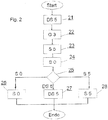
- FIG. 2 The flowchart shown describes a possible procedure of the computer system 1, which undergoes an interruption of the operating voltage in a deep sleep state DS5 in step 21.
- the primary mains AC voltage for supplying the power supply 2 completely fails. This corresponds to the ACPI state G3 (mechanical off), which is taken in step 22.
- the power supply 2 sets in In this case, neither the secondary operating voltage nor the secondary standby voltage ready.
- step 23 After restoring the primary supply voltage in step 23, initially only a standby voltage for the microcontroller 5 is provided. From this standby state, the computer system 1, for example according to a BIOS presetting, now at least temporarily assumes a fully functional operating state S0 in step 24 by providing the secondary supply voltage of the processor 4.
- step 25 in the operating state S0 Only in a further step 25 in the operating state S0 is it possible to make a selection of the possible operating states and, depending on information stored in the memory area of the firmware, optionally to return to the deep sleep state DS5 in step 27. Further options for terminating the method are staying in a fully functional state S0 in step 26 or changing to the standby state S5 in step 28.
- FIG. 3 shows the flow chart of a startup process of a computer system 1 according to an embodiment of the invention.
- information about an interruption of the at least one supply voltage is already stored in a memory 6 in step 31, for example in the deep sleep state DS5.
- Corresponding information can be, for example, an intentional or unintentional interruption of the secondary operating voltages, ie the operating voltage of the processor 4, standby voltage, and / or the maintenance voltage be set.
- the microcontroller may determine if there was a command from the system component 3 for an interrupt if the bistable toggle indicates an interruption in the power supply.
- the computer system 1 In the initial state of the illustrated sequence, the computer system 1 is in step 31 in an energy-saving deep sleep state DS5 and now experiences an interruption of the operating voltage, resulting in step 32 to an automatic change to the operating state G3.
- the power supply 2 After the operating voltage is restored, the power supply 2 initially provides only the standby voltage for the microcontroller 5 in step 33.
- the computer system 1 is for this purpose first in a so-called legacy state, which is similar in energy to the S5 state, but neither a BIOS code nor an operating system was loaded by the processor.
- the microcontroller 5 can recognize, based on the information contained in the memory 6 in this energy-saving state that an interruption of a power supply has taken place.
- the memory contents indicate that an interruption of the secondary operating and standby voltages was intended, for example, because a change to the deep sleep state DS5 was signaled by the system component 3 before the interruption.
- the memory contents would indicate an inadvertent interruption.
- the microcontroller 5 is now able to perform a query in step 34, which operating state is to be taken next.
- an unintended disconnection of the primary supply voltage may be responded in accordance with a BIOS preset.
- a BIOS preset For example, a previously used and stored operating state, such as, in particular, the standby state S5 or the deep sleep state DS5 can be resumed.
- the operating state S0 is assumed.
- the microcontroller 5 ensures that the last used or desired state is taken; for example, by generating a wake-up event to assume the operating state S0 in step 35, by maintaining the S5 state or by switching to the operating state DS5 in step 36.
- the described computer system 1 or the start procedure described represent an advantageous combination of an energetically particularly favorable deep sleep state with a flexible wake-up behavior of the computer when reapplying an operating voltage.
Landscapes
- Engineering & Computer Science (AREA)
- Theoretical Computer Science (AREA)
- General Engineering & Computer Science (AREA)
- Physics & Mathematics (AREA)
- General Physics & Mathematics (AREA)
- Computer Hardware Design (AREA)
- Computing Systems (AREA)
- Power Sources (AREA)
- Microcomputers (AREA)
Description
- Die Erfindung betrifft ein Computersystem aufweisend ein Netzteil zur Umwandlung einer primären Versorgungsspannung in wenigstens eine sekundäre Betriebsspannung und wenigstens eine sekundäre Bereitschaftsspannung sowie eine Systemkomponente umfassend wenigstens einen Prozessor. Das Computersystem ist dazu eingerichtet, in einem ersten Betriebszustand den wenigstens einen Prozessor mit der wenigstens einen sekundären Betriebsspannung zu versorgen.
- Zum Stand der Technik gehört der von den Firmen Hewlett Packard Corporation, Intel Corporation, Microsoft Corporation, Phoenix Technologies Ltd. und der Toshiba Corporation entwickelte Industriestandard "Advanced Configuration and Power Interface Specification", kurz ACPI (Stand 6. Dezember 2011), der unter anderem verschiedene Betriebszustände eines Computersystems beschreibt. So bezeichnet der Zustand S0 einen Arbeitszustand, die Zustände S1 bis S4 verschiedene Schlafzustände des Systems und der Zustand S5 einen sogenannten Soft-off- oder Bereitschaftszustand. Durch das Einnehmen eines Zustandes mit geringer Leistungsaufnahme, wie zum Beispiel den Schlafzuständen oder dem Bereitschaftszustand, ist es dem Computersystem möglich, Energie zu sparen.
- Die
US 2012/0117364 A1 beschreibt ein Betriebsverfahren für einen Taschenrechner mit einem kontrollierbaren Leistungsbereich. Das Verfahren umfasst das Empfangen eines Signals zum Herunterfahren, das Speichern von Kontext Informationen wenigstens einer Komponente des kontrollierbaren Leistungsbereichs in einen externen Speicher und das Setzen eines Boot-Indikators um einen Schnellstart beim Einschalten anzuzeigen. Das Verfahren umfasst des Weiteren sind das wegnehmen von Leistung von dem kontrollierbaren Leistungsbereich. - Aus der
US 2009/0207423 A1 ist ein Informationsverarbeitungsgerät bekannt, das mehrere arithmetische Einheiten und mehrere Speichereinheiten aufweist und bei dem ein Leistungsverbrauch in einem Energiesparzustand reduziert wird. Des Weiteren wird eine Rückkehrzeit von dem Energiesparzustand in einen normalen Zustand reduziert. - Aufgabe der vorliegenden Erfindung ist es, ein Computersystem zu beschreiben, dessen Energieeffizienz gegenüber bekannten Systemen noch weiter verbessert ist.
- Gemäß einem ersten Aspekt der Erfindung wird ein Computersystem beschrieben, das ein Netzteil zur Umwandlung einer primären Versorgungsspannung in wenigstens eine sekundäre Betriebsspannung und wenigstens eine sekundäre Bereitschaftsspannung, eine Systemkomponente umfassend wenigstens einen Prozessor, einen Mikrocontroller und einen mit dem Mikrocontroller funktionsfähig verbundenen Speicher zum Speichern von Informationen über eine Unterbrechung wenigstens einer Betriebsspannung des Computersystems aufweist. Der Speicherinhalt zeigt an, ob eine Unterbrechung der sekundären Betriebs- und Bereitschaftsspannung beabsichtigt war oder ob es sich um eine unbeabsichtigte Unterbrechung der sekundären Betriebs- und Bereitschaftsspannung handelt. Das Computersystem ist dazu eingerichtet, in einem ersten Betriebszustand den wenigstens einen Prozessor mit der wenigstens einen sekundären Betriebsspannung zu versorgen. Des Weiteren ist das Computersystem dazu eingerichtet, in einem zweiten Betriebszustand den wenigstens einen Prozessor von der wenigstens einen sekundären Betriebsspannung zu trennen und den Mikrocontroller mit der wenigstens einen sekundären Bereitschaftsspannung zu versorgen. In einem dritten Betriebszustand ist das Computersystem dazu eingerichtet, sowohl den wenigstens einen Prozessor und den Mikrocontroller von der Betriebsspannung bzw. der Bereitschaftsspannung zu trennen. Der Mikrocontroller ist dazu eingerichtet, beim Anlegen der wenigstens einen sekundären Bereitschaftsspannung an den Mikrocontroller die Informationen über die Unterbrechung wenigstens einer Betriebsspannung des Computersystems aus dem Speicher auszulesen und das Computersystem in Abhängigkeit der ausgelesenen Informationen bei einer beabsichtigten Unterbrechung mit dem Erfassen eines nachfolgenden Einschaltsignals in den ersten Betriebszustand zu schalten und der Mikrocontroller dazu eingerichtet ist, bei einer unbeabsichtigten Unterbrechung eine Speicherabfrage durchzuführen, welcher Betriebszustand als nächstes eingenommen werden soll.
- Durch das Auslesen der Informationen über die Unterbrechung wenigstens einer Betriebsspannung des Computersystems durch den Mikrocontroller wird es möglich unterschiedliche Gründe für die Unterbrechung einer primären Versorgungsspannung, der sekundären Betriebsspannung und/oder der sekundären Bereitschaftsspannung zu ermitteln. Hierdurch kann beim Wiederanlegen einer Bereitschaftsspannung auf eine gegebenenfalls unnötige Stromversorgung des Prozessors in dem ersten Betriebszustand verzichtet werden. Durch das Vermeiden des Startens des Prozessors, beispielsweise zum Ausführen von BIOS-Programmcode zur Auswahl eines Betriebszustands für das Computersystem, wird eine Energieeinsparung erreicht.
- In einer vorteilhaften Ausgestaltung umfasst der Speicher eine bistabile Kippstufe, die von dem Netzteil in dem ersten, zweiten und dritten Betriebszustand mit einer Erhaltungsspannung versorgt wird. Dabei zeigt ein erster Zustand der bistabilen Kippstufe an, dass das Computersystem eine Unterbrechung der sekundären Bereitschaftsspannung erfahren hat. Ein Vorteil dieser Ausführung ist, dass sie
einfach mit Hilfe einer diskreten Schaltung realisiert werden kann. - Weiter ist es vorgesehen, dass die bistabile Kippstufe nach einer Unterbrechung einer Erhaltungsspannung einen vorbestimmten zweiten Zustand einnimmt, wobei der zweite Zustand der bistabilen Kippstufe anzeigt, dass das Computersystem eine Unterbrechung der primären Versorgungsspannung erfahren hat. Hierdurch ist es dem Mikrocontroller möglich, eine Unterbrechung der primären Versorgung als solche zu erkennen und von einer beabsichtigten Unterbrechung der sekundären Bereitschaftsspannung des Mikrocontrollers zu unterscheiden.
- In einer alternativen Ausgestaltung ist der Speicher ein nichtflüchtiger Speicher, wie zum Beispiel ein Flash- oder ein EEPROM-Speicher und somit fähig, Informationen auch nach einer Unterbrechung der primären Betriebsspannung oder über einen sonstigen Energieausfall hinweg zu speichern.
- Gemäß einer weiteren vorteilhaften Ausführung ist das Computersystem dadurch gekennzeichnet, dass das Computersystem des Weiteren einen nichtflüchtigen Speicherbaustein zum Speichern von ausführbarem Programmcode aufweist. Dabei umfasst der Programmcode eine Routine zur Auswahl eines einer Mehrzahl von möglichen Betriebszuständen des Computersystems. Durch diese Ausgestaltung ist das System in der Wahl unterschiedlicher Zustände besonders flexibel.
- Ein weiterer Aspekt der Erfindung umfasst ein Verfahren zum Betrieb eines Computersystems, aufweisend wenigstens einen Prozessor, einen Mikrocontroller und einen Speicher, wobei das Computersystem dazu eingerichtet ist, in einem ersten Betriebszustand den wenigstens einen Prozessor mit der wenigstens einen sekundären Betriebsspannung zu versorgen und des Weiteren dazu eingerichtet ist, in einem zweiten Betriebszustand den wenigstens einen Prozessor von der wenigstens einen sekundären Betriebsspannung zu trennen und den Mikrocontroller mit der wenigstens einen sekundären Bereitschaftsspannung zu versorgen. Darüber hinaus ist das Computersystem dazu eingerichtet, einen dritten Betriebszustand anzunehmen, in dem der wenigstens eine Prozessor von der wenigstens einen sekundären Betriebsspannung und der Mikrocontroller von der wenigstens einen Bereitschaftsspannung getrennt sind. Das Verfahren umfasst wenigstens die Schritte:
- Speichern von Informationen über eine Unterbrechung wenigstens einer Betriebsspannung des Computersystems, wobei ein Speicherinhalt anzeigt, ob eine Unterbrechung der sekundären Betriebs- und Bereitschaftsspannung beabsichtigt war oder ob es sich um eine unbeabsichtigte Unterbrechung der sekundären Betriebs- und Bereitschaftsspannung handelt,
- Erkennen, dass wenigstens eine sekundäre Bereitschaftsspannung an den Mikrocontroller angelegt wurde,
- Auslesen der Informationen über die Unterbrechung wenigstens einer Betriebsspannung des Computersystems durch den Mikrocontroller,
- Schalten des Computersystems wahlweise in den ersten Betriebszustand abhängig von den von dem Mikrocontroller aus dem Speicher ausgelesenen Informationen, wobei das
- Computersystem bei einer beabsichtigten Unterbrechung mit dem Erfassen eines nachfolgenden Einschaltsignals in den ersten Betriebszustand geschaltet wird und bei einer unbeabsichtigten Unterbrechung eine Speicherabfrage durch den Mikrocontroller durchgeführt wird, welcher Betriebszustand als nächstes eingenommen werden soll..
- Hierbei liegt ein Vorteil des Verfahrens darin, in Abhängigkeit einer Auswertung der gespeicherten Informationen durch den Mikrocontroller, eine beabsichtigte von einer unbeabsichtigten Unterbrechung einer Betriebsspannung zu unterscheiden ohne einen ersten Betriebszustand einzunehmen. Durch das Verbleiben in dem zweiten Zustand kann im Vergleich zu einem Wechsel in einen ersten Betriebszustand Energie eingespart werden.
- Unterschiedliche Ausführungsbeispiele der Erfindung werden nachfolgend unter Bezugnahme auf die angehängten Figuren beschrieben. In den Figuren zeigen:
Figur 1 ein Blockdiagramm eines Computersystems,Figur 2 ein Ablaufdiagramm eines möglichen Startvorgangs eines Computersystems, - Figur 3
- ein Ablaufdiagramm eines Startvorgangs eines Computersystems gemäß einer Ausgestaltung der Erfindung.
- Das Blockdiagramm gemäß
Figur 1 zeigt schematisch ein Computersystem 1. Das Computersystem 1 umfasst im dargestellten Ausführungsbeispiel ein Netzteil 2 sowie eine Systemkomponente 3. Die Systemkomponente 3 umfasst einen Prozessor 4. Das Computersystem 1 umfasst des Weiteren einen Mikrocontroller 5 und einen Speicher 6. Obwohl die Komponenten 5 und 6 in derFigur 1 als eigenständige Bauteile dargestellt sind, können sie selbstverständlich auch in das Netzteil 2 oder die Systemkomponente 3 integriert werden. - Das Netzteil 2 nimmt eine primäre Versorgungsspannung in Form einer Netzwechselspannung auf und wandelt diese in eine oder mehrere sekundäre Betriebsspannungen um. Insbesondere erzeugt es eine erste Betriebsspannung für die Systemkomponente 3 und den darauf angeordneten Prozessor 4 und eine zweite Betriebsspannung für den Mikrocontroller 5. Die zweite Betriebsspannung wird von dem Netzteil 2 auch in einem Bereitschaftszustand, beispielsweise dem ACPI-Zustand S5, bereitgestellt und daher im Folgenden als Bereitschaftsspannung bezeichnet. Der Mikrocontroller 5 und der Speicher 6 sind derart verbunden, dass sie Daten austauschen können beziehungsweise der Mikrocontroller 5 Daten in dem Speicher 6 speichern und Daten aus dem Speicher 6 abrufen kann.
- Beispielsweise handelt es sich bei dem Speicher 6 um eine Flip-Flop-Schaltung die mit einem programmierbaren Eingabe-/Ausgabeanschluss des Mikrocontrollers 5 verbunden ist. Die Flip-Flop-Schaltung wird dabei von dem Netzteil 2 oder einer anderen Energiequelle, wie beispielsweise einer sogenannten BIOS-Batterie, stets, also in allen Betriebszuständen, mit einer Spannung zur Erhaltung des Speicherinhalts versorgt. In einer alternativen Ausführung ist der Speicher 6 als nichtflüchtiger Speicherbaustein ausgeführt, der über eine oder mehrere Busleitungen mit dem Mikrocontroller 5 verbunden ist.
- Erfährt das Computersystem 1 eine Unterbrechung der sekundären Betriebsspannung und wird nachfolgend eine Bereitschaftsspannung an den Mikrocontroller 5 angelegt, so kann dieser die vorübergehende Unterbrechung der Betriebsspannung erkennen und liest aus dem Speicher 6 Informationen über die Unterbrechung der Betriebsspannung aus. Eine Unterbrechung der Betriebsspannung kann beispielsweise durch ein gewünschtes Abschalten des Computersystems 1, durch ein Ziehen des Netzsteckers oder mechanisches Abschalten des Netzteils 2 oder eine netzseitige Störung der primären Versorgungsspannung verursacht werden. Auf Grundlage der ausgelesenen Informationen kann der Mikrocontroller 5 die Ursache der Unterbrechung bestimmen und kann das Computersystem 1 daraufhin wahlweise in einen ersten oder einen anderen Betriebszustand versetzen.
- In der beschriebenen Ausgestaltung handelt es sich bei den unterschiedlichen Betriebszuständen um Betriebszustände mit unterschiedlichem Energieverbrauch des Computersystems 1. So entspricht der erste Betriebszustand, in welchem das gesamte Computersystem 1 mit einer Betriebsspannung versorgt wird, einem Betriebszustand mit hohem Energieverbrauch, der in dem ACPI-Standard als S0-Zustand bezeichnet wird. Bei dem zweiten Betriebszustand handelt es sich um einen energetisch günstigeren Betriebszustand des Computersystems 1, bei dem nur ausgewählte Komponenten wie beispielsweise der Mikrocontroller 5 und der Speicher 6 mit einer Bereitschaftsspannung versorgt werden und andere Komponenten des Computersystems 1 wie der Prozessor 4 von einer Betriebsspannung getrennt sind. In diesem Zustand können auch weitere Komponenten, wie beispielsweise eine Netzwerkkarte oder ein Echtzeitbaustein mit der Bereitschaftsspannung versorgt werden, um ein Aufwecken des Computersystems 1 aus dem Bereitschaftszustand zu ermöglichen. Bei diesem Betriebszustand kann es sich beispielsweise um den ACPI-Zustand S5 handeln. In einem weiteren Betriebszustand, einem sogenannten Tiefschlafzustand, der außerhalb der genannten ACPI-Spezifikation liegt, ist fast das gesamte Computersystem 1 von einer Betriebsspannung getrennt. Lediglich der Speicher 6, sofern er ein flüchtiger Speicher ist, und gegebenenfalls eine Überwachungsschaltung für einen Einschalttaster werden von dem Netzteil 2 mit einer Erhaltungsspannung versorgt.
- In der beschriebenen Ausgestaltung umfasst der Speicher 6 eine bistabile Kippstufe, wobei ein Zustand der bistabilen Kippstufe anzeigt, dass das Computersystem 1 eine Unterbrechung der primären Versorgungsspannung, die im ACPI-Standard als G3 bezeichnet wird, erfahren hat, ohne dass dies von dem Computersystem 1 initiiert wurde. In dieser Ausführung ist der Speicher 6 mit dem Netzteil 2 verbunden und das Netzteil 2 dazu eingerichtet, den Speicher 6 sowohl in dem ersten Betriebszustand, dem zweiten Betriebszustand als auch in dem dritten Betriebszustand mit einer Erhaltungsspannung zu versorgen. Die bistabile Kippstufe nimmt nach einer Unterbrechung der Erhaltungsspannung einen zurückgesetzten Zustand ein, wobei der zurückgesetzte Zustand der bistabilen Kippstufe anzeigt, dass die primäre Stromversorgung zu dem Netzteil 2 unterbrochen wurde.
- Beispielsweise zeigt eine Schaltung mit der bistabilen Kippstufe bei Bereitstellung der Bereitschaftsspannung eine Unterbrechung der primären Versorgungsspannung (englisch: "AC-Fail") an. Die Unterbrechung der primären Spannung wird beispielsweise erkannt, wenn die sekundäre Betriebsspannung nicht mehr vorhanden ist obwohl die Systemkomponente 3 zuvor keine Abschaltung angezeigt hat oder wenn die Versorgungsspannung der bistabilen Kippstufe nicht mehr vorhanden ist. Dabei ist die erste Erkennung im ACPI-Zustand S0 aktiv und die zweite Erkennung wird für die Übergänge aus dem ACPI-Zustand S5 oder dem Tiefschlafzustand DS5 in den Zustand G3 verwendet.
- Dadurch, dass der Speicher 6 auch im Tiefschlafzustand DS5 mit einer Erhaltungsspannung versorgt wird und der Speicher 6 Informationen zu einer Spannungsunterbrechung speichert, ist es dem Mikrocontroller 5 in der beschriebenen Ausführung der Erfindung möglich, im Betriebszustand S5 eine Auswahl 34 auszuführen, welche es dem Computersystem 1 erlaubt, einen von mehreren hinterlegten Betriebszuständen einzunehmen.
- Zum besseren Verständnis der Erfindung werden anhand der
Figuren 2 und3 unterschiedliche Startverfahren einander gegenübergestellt. - Das in
Figur 2 dargestellte Ablaufdiagramm beschreibt ein mögliches Vorgehen des Computersystems 1, welches in einem Tiefschlafzustand DS5 in Schritt 21 eine Unterbrechung der Betriebsspannung erfährt. Beispielsweise fällt die primäre Netzwechselspannung zur Versorgung des Netzteils 2 komplett aus. Dies entspricht dem ACPI-Zustand G3 (mechanisch aus), der in Schritt 22 eingenommen wird. Das Netzteil 2 stellt in diesem Fall weder die sekundäre Betriebsspannung noch die sekundäre Bereitschaftsspannung bereit. - Nach dem Wiederherstellen der primären Versorgungsspannung in Schritt 23 wird zunächst lediglich eine Bereitschaftsspannung für den Mikrocontroller 5 zur Verfügung gestellt. Aus diesem Bereitschaftszustand nimmt das Computersystem 1, beispielsweise gemäß einer BIOS-Voreinstellung, nun in Schritt 24 durch Bereitstellen der sekundären Versorgungsspannung des Prozessors 4 zumindest vorübergehend einen voll funktionsfähigen Betriebszustand S0 ein.
- Erst in einem weiteren Schritt 25 im Betriebszustand S0 ist es möglich, eine Auswahl über die möglichen Betriebszustände zu treffen und in Abhängigkeit von in dem Speicherbereich der Firmware gespeicherten Informationen wahlweise im Schritt 27 in den Tiefschlafzustand DS5 zurückzukehren. Weitere Möglichkeiten für ein Beenden des Verfahrens sind das Verbleiben in einem voll funktionsfähigen Zustand S0 im Schritt 26 oder das Wechseln in den Bereitschaftszustand S5 in Schritt 28.
-
Figur 3 zeigt das Ablaufdiagramm eines Startvorgangs eines Computersystems 1 gemäß einer Ausgestaltung der Erfindung. - In der beschriebenen Ausgestaltung werden Informationen über eine Unterbrechung der wenigstens einen Versorgungsspannung bereits zuvor, beispielsweise in dem Tiefschlafzustand DS5, in Schritt 31 in einem Speicher 6 abgelegt. Entsprechende Informationen können beispielsweise bei einer beabsichtigten oder unbeabsichtigten Unterbrechung der sekundären Betriebsspannungen, also der Betriebsspannung des Prozessors 4, Bereitschaftsspannung, und/oder der Erhaltungsspannung gesetzt werden. Alternativ oder zusätzlich kann der Mikrocontroller nach einem Wiederherstellen der Bereitschaftsspannung feststellen, ob es ein Kommando aus der Systemkomponente 3 für eine Unterbrechung gab, wenn die bistabile Kippstufe eine Unterbrechung der Stromversorgung anzeigt.
- Im Ausgangszustand des dargestellten Ablaufs befindet sich das Computersystem 1 in Schritt 31 in einem energiesparenden Tiefschlafzustand DS5 und erfährt nun eine Unterbrechung der Betriebsspannung, was in Schritt 32 zu einem automatischen Wechseln in den Betriebszustand G3 führt.
- Nachdem die Betriebsspannung wiederhergestellt ist, stellt das Netzteil 2 in Schritt 33 zunächst nur die Bereitschaftsspannung für den Mikrocontroller 5 bereit. Das Computersystem 1 befindet sich hierfür zunächst in einem sogenannten Legacy-Zustand, der energetisch dem S5-Zustand ähnelt, wobei jedoch weder ein BIOS-Code noch ein Betriebssystem durch den Prozessor geladen wurde. Der Mikrocontroller 5 kann auf Grundlage der in dem Speicher 6 enthaltenen Informationen in diesem energiesparenden Zustand erkennen, dass eine Unterbrechung einer Spannungsversorgung stattgefunden hat. Beispielsweise zeigt der Speicherinhalt an, dass eine Unterbrechung der sekundären Betriebs- und Bereitschaftsspannungen beabsichtigt war, beispielsweise weil vor der Unterbrechung von der Systemkomponente 3 ein Wechsel in den Tiefschlafzustand DS5 signalisiert wurde. Bei der oben genannten Störung der primären Versorgungsspannung, würde der Speicherinhalt dagegen eine unbeabsichtigte Unterbrechung anzeigen.
- Dementsprechend ist der Mikrocontroller 5 nun in der Lage, in Schritt 34 eine Abfrage durchzuführen, welcher Betriebszustand als nächstes eingenommen werden soll. Beispielsweise kann auf eine unbeabsichtigte Trennung der primären Versorgungsspannung gemäß einer BIOS-Voreinstellung reagiert werden. Beispielsweise kann ein zuvor verwendeter und gespeicherter Betriebszustand, wie insbesondere der Bereitschaftszustand S5 oder der Tiefschlafzustand DS5 erneut eingenommen werden. Bei einer beabsichtigen Unterbrechung mit dem Erfassen eines nachfolgenden Einschaltsignals (englisch: "power button request") wird dagegen anforderungsgemäß der Betriebszustand S0 eingenommen. Dabei sorgt der Mikrocontroller 5 dafür, dass der zuletzt verwendete oder gewünschte Zustand eingenommen wird; beispielsweise durch Erzeugen eines Aufwachereignisses zum Einnehmen des Betriebszustands S0 in Schritt 35, durch Beibehaltung des S5-Zustands oder durch ein Wechseln in den Betriebszustand DS5 in Schritt 36.
- Das beschriebene Computersystem 1 bzw. der beschriebene Startvorgang stellen eine vorteilhafte Kombination eines energetisch besonders günstigen Tiefschlafzustands mit einem flexiblen Aufwachverhalten des Computers beim Wiederanlegen einer Betriebsspannung dar.
-
- 1
- Computersystem
- 2
- Netzteil
- 3
- Systemkomponente
- 4
- Prozessor
- 5
- Mikrocontroller
- 6
- Speicher
- 21 - 28
- Verfahrensschritte
- 31 - 37
- Verfahrensschritte
- S0
- voll funktionsfähiger Betriebzustand
- S5
- Bereitschaftszustand
- DS5
- Tiefschlafzustand
- G3
- mechanisch ausgeschalteter Zustand
Claims (7)
- Computersystem (1), aufweisend:- ein Netzteil (2) zur Umwandlung einer primären Versorgungsspannung in wenigstens eine sekundäre Betriebsspannung und wenigstens eine sekundäre Bereitschaftsspannung;- eine Systemkomponente (3) umfassend wenigstens einen Prozessor (4);- einen Mikrocontroller (5) und- einen mit dem Mikrocontroller (5) funktionsfähig verbundenen Speicher (6) zum Speichern von Informationen über eine Unterbrechung wenigstens einer Betriebsspannung des Computersystems (1), wobei dessen Speicherinhalt anzeigt, ob eine Unterbrechung der sekundären Betriebs- und Bereitschaftsspannung beabsichtigt war oder ob es sich um eine unbeabsichtigte Unterbrechung der sekundären Betriebs- und Bereitschaftsspannung handelt;wobei- das Computersystem (1) dazu eingerichtet ist, in einem ersten Betriebszustand den wenigstens einen Prozessor (4) mit der wenigstens einen sekundären Betriebsspannung zu versorgen;- das Computersystem (1) des Weiteren dazu eingerichtet ist, in einem zweiten Betriebszustand den wenigstens einen Prozessor (4) von der wenigstens einen sekundären Betriebsspannung zu trennen und den Mikrocontroller (5) mit der wenigstens einen sekundären Bereitschaftsspannung zu versorgen;- das Computersystem (1) des Weiteren dazu eingerichtet ist, in einem dritten Betriebszustand den wenigstens einen Prozessor (4) von der wenigstens einen sekundären Betriebsspannung und den Mikrocontroller (5) von der wenigstens einen sekundären Bereitschaftsspannung zu trennen und- der Mikrocontroller (5) dazu eingerichtet ist, beim Anlegen der wenigstens einen sekundären Bereitschaftsspannung an den Mikrocontroller (5) die Informationen über die Unterbrechung der wenigstens einen Betriebsspannung des Computersystems (1) aus dem Speicher (6) auszulesen und das Computersystem (1) in Abhängigkeit der ausgelesenen Informationen bei einer beabsichtigten Unterbrechung mit dem Erfassen eines nachfolgenden Einschaltsignals in den ersten Betriebszustand zu schalten und bei einer unbeabsichtigten Unterbrechung eine Speicherabfrage durchzuführen, welcher Betriebszustand als nächstes eingenommen werden soll.
- Computersystem (1) nach Anspruch 1,
gekennzeichnet dadurch, dass
der erste Betriebszustand einem aktiven Zustand mit einer ersten Leistungsaufnahme, der zweite Betriebszustand einem Bereitschaftszustand mit einer gegenüber der ersten Leistungsaufnahme reduzierten zweiten Leistungsaufnahme und der dritte Betriebszustand einem Tiefschlafzustand mit einer gegenüber der zweiten Leistungsaufnahme reduzierten dritten Leistungsaufnahme entspricht. - Computersystem (1) nach Anspruch 1 oder 2,
dadurch gekennzeichnet, dass
der Speicher (6) eine bistabile Kippstufe umfasst, die von dem Netzteil (2) in dem ersten, zweiten und dritten Betriebszustand mit einer Erhaltungsspannung versorgt wird, wobei ein erster Zustand der bistabilen Kippstufe anzeigt, dass das Computersystem (1) eine Unterbrechung der sekundären Bereitschaftsspannung erfahren hat. - Computersystem (1) nach Anspruch 3,
dadurch gekennzeichnet, dass
die bistabile Kippstufe nach einer Unterbrechung der Erhaltungsspannung einen vorbestimmten zweiten Zustand einnimmt, wobei der zweite Zustand der bistabilen Kippstufe anzeigt, dass das Computersystem (1) eine Unterbrechung der primären Versorgungsspannung erfahren hat. - Computersystem (1) nach einem der Ansprüche 1 oder 2,
dadurch gekennzeichnet, dass
der Speicher (6) ein nichtflüchtiger Speicher, insbesondere ein Flash-Speicher oder ein EEPROM-Speicher, ist. - Computersystem (1) nach einem der Ansprüche 1 bis 5,
dadurch gekennzeichnet, dass
das Computersystem (1) des Weiteren einen nicht-flüchtigen Speicherbaustein zum Speichern von ausführbarem Programmcode aufweist, wobei der Programmcode eine Routine zur Auswahl eines einer Mehrzahl von möglichen Betriebszuständen des Computersystems (1) umfasst. - Verfahren zum Betrieb eines Computersystems, aufweisend wenigstens einen Prozessor (4), einen Mikrocontroller (5) und einen Speicher (6), wobei das Computersystem (1) dazu eingerichtet ist, in einem ersten Betriebszustand den wenigstens einen Prozessor (4) mit wenigstens einer sekundären Betriebsspannung zu versorgen, in einem zweiten Betriebszustand den wenigstens einen Prozessor (4) von der wenigstens einen sekundären Betriebsspannung zu trennen und den Mikrocontroller (5) mit wenigstens einer sekundären Bereitschaftsspannung zu versorgen und in einem dritten Betriebszustand den wenigstens einen Prozessor (4) von der wenigstens einen sekundären Betriebsspannung und den Mikrocontroller (5) von der wenigstens einen sekundären Bereitschaftsspannung zu trennen, wobei das Verfahren wenigstens die folgenden Schritte umfasst:- Speichern von Informationen über eine Unterbrechung wenigstens einer Betriebsspannung des Computersystems (1), wobei ein Speicherinhalt anzeigt, ob eine Unterbrechung der sekundären Betriebs- und Bereitschaftsspannung beabsichtigt war oder ob es sich um eine unbeabsichtigte Unterbrechung der sekundären Betriebs- und Bereitschaftsspannung handelt;- Erkennen, dass wenigstens eine sekundäre Bereitschaftsspannung an einen Mikrocontroller (5) angelegt wurde;- Auslesen der Informationen über die Unterbrechung der wenigstens einer Betriebsspannung des Computersystems (1) durch den Mikrocontroller (5) und- Schalten des Computersystems (1) wahlweise in den ersten Betriebszustand abhängig von den von dem Mikrocontroller (5) aus dem Speicher (6) ausgelesenen Informationen, wobei das Computersystem bei einer beabsichtigten Unterbrechung mit dem Erfassen eines nachfolgenden Einschaltsignals in den ersten Betriebszustand geschaltet wird und bei einer unbeabsichtigten Unterbrechung eine Speicherabfrage durch den Mikrocontroller durchgeführt wird, welcher Betriebszustand als nächstes eingenommen werden soll.
Applications Claiming Priority (2)
| Application Number | Priority Date | Filing Date | Title |
|---|---|---|---|
| DE102012105986A DE102012105986B3 (de) | 2012-07-04 | 2012-07-04 | Computersystem und Verfahren zum Betrieb eines Computersystems |
| PCT/EP2013/063831 WO2014005995A1 (de) | 2012-07-04 | 2013-07-01 | Computersystem und verfahren zum betrieb eines computersystems |
Publications (2)
| Publication Number | Publication Date |
|---|---|
| EP2820508A1 EP2820508A1 (de) | 2015-01-07 |
| EP2820508B1 true EP2820508B1 (de) | 2016-12-14 |
Family
ID=47740419
Family Applications (1)
| Application Number | Title | Priority Date | Filing Date |
|---|---|---|---|
| EP13732559.3A Not-in-force EP2820508B1 (de) | 2012-07-04 | 2013-07-01 | Computersystem und verfahren zum betrieb eines computersystems |
Country Status (5)
| Country | Link |
|---|---|
| US (1) | US9933839B2 (de) |
| EP (1) | EP2820508B1 (de) |
| JP (1) | JP6085673B2 (de) |
| DE (1) | DE102012105986B3 (de) |
| WO (1) | WO2014005995A1 (de) |
Families Citing this family (2)
| Publication number | Priority date | Publication date | Assignee | Title |
|---|---|---|---|---|
| KR101657593B1 (ko) * | 2016-05-18 | 2016-09-19 | (주)이엠텍아이엔씨 | 컴퓨터 시스템의 동작상태 측정 방법 및 이를 활용한 절전 방법 |
| DE102024210557B3 (de) | 2024-11-04 | 2025-08-14 | Infineon Technologies Ag | Fehlerfallrückschreibung |
Citations (1)
| Publication number | Priority date | Publication date | Assignee | Title |
|---|---|---|---|---|
| US20120117364A1 (en) * | 2010-11-04 | 2012-05-10 | Russell Melvin Rosenquist | Method and System for Operating a Handheld Calculator |
Family Cites Families (17)
| Publication number | Priority date | Publication date | Assignee | Title |
|---|---|---|---|---|
| DE3808863A1 (de) | 1988-03-17 | 1989-09-28 | Philips Patentverwaltung | Stromversorgungsanordnung |
| JP3168471B2 (ja) | 1991-10-14 | 2001-05-21 | 三洋電機株式会社 | エアフィルタ |
| JP2000155601A (ja) | 1998-11-18 | 2000-06-06 | Sanyo Electric Co Ltd | 制御装置及びこの制御装置を備えた空気調和装置 |
| US6501999B1 (en) * | 1999-12-22 | 2002-12-31 | Intel Corporation | Multi-processor mobile computer system having one processor integrated with a chipset |
| US20020108064A1 (en) * | 2001-02-07 | 2002-08-08 | Patrick Nunally | System and method for optimizing power/performance in network-centric microprocessor-controlled devices |
| JP3456208B2 (ja) | 2001-07-18 | 2003-10-14 | 株式会社日立製作所 | 磁気ディスク装置の制御方法及び電力環境適応型磁気ディスク装置 |
| JP3848152B2 (ja) | 2001-12-20 | 2006-11-22 | 株式会社東芝 | 多機能icカード |
| US7730335B2 (en) * | 2004-06-10 | 2010-06-01 | Marvell World Trade Ltd. | Low power computer with main and auxiliary processors |
| US8384700B2 (en) * | 2007-01-26 | 2013-02-26 | Microsoft Corporation | Linked shell |
| US7917784B2 (en) * | 2007-01-07 | 2011-03-29 | Apple Inc. | Methods and systems for power management in a data processing system |
| JP2008204209A (ja) * | 2007-02-21 | 2008-09-04 | Sony Corp | 電子機器、復帰用インターフェース設定方法、復帰通信方法及びコンピュータプログラム |
| TW200840358A (en) * | 2007-03-16 | 2008-10-01 | Benq Corp | Method for managing a scheduling system and related scheduling system |
| CN101689106B (zh) * | 2007-06-12 | 2013-10-09 | 松下电器产业株式会社 | 多处理器控制装置、多处理器控制方法以及多处理器控制电路 |
| JP5207792B2 (ja) * | 2008-02-19 | 2013-06-12 | キヤノン株式会社 | 情報処理装置及び情報処理方法 |
| JP4703757B2 (ja) | 2009-11-18 | 2011-06-15 | 株式会社東芝 | 情報処理装置 |
| TWM412423U (en) * | 2010-08-13 | 2011-09-21 | Micro Star Int Co Ltd | Computer motherboard for reducing power consumption during sleep mode |
| JP5696480B2 (ja) * | 2011-01-04 | 2015-04-08 | 株式会社リコー | 制御装置、ネットワークに接続可能な装置、制御方法及び制御プログラム |
-
2012
- 2012-07-04 DE DE102012105986A patent/DE102012105986B3/de not_active Expired - Fee Related
-
2013
- 2013-07-01 EP EP13732559.3A patent/EP2820508B1/de not_active Not-in-force
- 2013-07-01 JP JP2015512088A patent/JP6085673B2/ja not_active Expired - Fee Related
- 2013-07-01 US US14/412,563 patent/US9933839B2/en not_active Expired - Fee Related
- 2013-07-01 WO PCT/EP2013/063831 patent/WO2014005995A1/de not_active Ceased
Patent Citations (1)
| Publication number | Priority date | Publication date | Assignee | Title |
|---|---|---|---|---|
| US20120117364A1 (en) * | 2010-11-04 | 2012-05-10 | Russell Melvin Rosenquist | Method and System for Operating a Handheld Calculator |
Also Published As
| Publication number | Publication date |
|---|---|
| DE102012105986B3 (de) | 2013-03-14 |
| WO2014005995A1 (de) | 2014-01-09 |
| JP6085673B2 (ja) | 2017-02-22 |
| US20150199001A1 (en) | 2015-07-16 |
| EP2820508A1 (de) | 2015-01-07 |
| JP2015524100A (ja) | 2015-08-20 |
| US9933839B2 (en) | 2018-04-03 |
Similar Documents
| Publication | Publication Date | Title |
|---|---|---|
| DE4413674C2 (de) | Stromversorgungs-Steuerungssystem für tragbare Datenverarbeitungsgeräte und Verfahren zum Betreiben dieses Systems | |
| DE102010032758B4 (de) | Computersystem, Verfahren zum Programmieren einer Echtzeituhr und Computerprogrammprodukt | |
| DE69333442T2 (de) | Bereitschaftssystem mit geringem Energieverbrauch für einen Monitor | |
| DE102018101028B3 (de) | Mikrocontrollersystem mit schaltungsinternem Debugger | |
| DE102008043947B4 (de) | Anschlusszustandserkennungssystem für ein Netzwerkkabel | |
| DE112018004746T5 (de) | Systeme und verfahren zum verwalten von durch einen mikrocontroller in einem inaktiven modus verbrauchter energie | |
| DE202009011250U1 (de) | Elektronisches Stromspargerät für Computer-Hauptplatinen (Motherboards) im "Standby-Speicher"-Zustand ("Suspend to Memory"-Status) | |
| DE10231160A1 (de) | Unterbrechungsfreie Leistungsversorgung mit Lastabwurf | |
| DE69027734T2 (de) | Personalrechner zur Verhinderung des Wiederaufnahmemodus bei Ersetzung einer Festplatte | |
| DE102008035103A1 (de) | Schnittstellenüberwachungsvorrichtung, Computersystem und Verfahren zum Überwachen eines differenziellen Schnittstellenanschlusses | |
| DE102010024154A1 (de) | Netzteil, Verarbeitungssystem und Steuerverfahren | |
| EP2159667B1 (de) | Computersystem und Verfahren zum Energie sparenden Betrieb eines Computersystems | |
| DE102013218385B4 (de) | Stromversorgungssystem | |
| DE112012004063T5 (de) | Stromversorgungseinheit und Steuerverfahren dafür | |
| DE102014101509A1 (de) | System und Verfahren zur Erlangung von Energie und zur Auslösung eines Leitungsunterbrechers von einer externen Einrichtung | |
| EP2063342B1 (de) | Stromversorgungsschaltung für ein elektronisches Gerät, Computer mit einer Stromversorgungsschaltung und Energiesparverfahren | |
| DE102012105986B3 (de) | Computersystem und Verfahren zum Betrieb eines Computersystems | |
| EP3479196B1 (de) | Computersystem mit wenigstens einer schnittstelle und verfahren | |
| DE10121935A1 (de) | Rücksetz-Anordnung für einen Mikrokontroller | |
| EP3558753B1 (de) | Niedrig-energie-betrieb von kraftfahrzeugfunktionen während des betriebes des kraftfahrzeuges | |
| EP1019799B1 (de) | Stromversorgungseinheit für rechnersysteme | |
| DE102015100855B3 (de) | Eingebettetes System, Betriebsverfahren und deren Verwendung | |
| DE102018103286B4 (de) | Computersystem, Betriebsverfahren für einen Mikrocontroller sowie Computerprogrammprodukt | |
| DE102007052880A1 (de) | Elektronische Stromversorgungseinheit, elektronisches Peripheriegerät, sowie Verfahren zur Steuerung einer Stromversorgungseinheit | |
| DE102014201590A1 (de) | Vorrichtungssteuereinrichtung und Vorrichtungssteuerverfahren |
Legal Events
| Date | Code | Title | Description |
|---|---|---|---|
| PUAI | Public reference made under article 153(3) epc to a published international application that has entered the european phase |
Free format text: ORIGINAL CODE: 0009012 |
|
| 17P | Request for examination filed |
Effective date: 20140930 |
|
| AK | Designated contracting states |
Kind code of ref document: A1 Designated state(s): AL AT BE BG CH CY CZ DE DK EE ES FI FR GB GR HR HU IE IS IT LI LT LU LV MC MK MT NL NO PL PT RO RS SE SI SK SM TR |
|
| AX | Request for extension of the european patent |
Extension state: BA ME |
|
| DAX | Request for extension of the european patent (deleted) | ||
| 17Q | First examination report despatched |
Effective date: 20151009 |
|
| GRAP | Despatch of communication of intention to grant a patent |
Free format text: ORIGINAL CODE: EPIDOSNIGR1 |
|
| INTG | Intention to grant announced |
Effective date: 20160714 |
|
| GRAS | Grant fee paid |
Free format text: ORIGINAL CODE: EPIDOSNIGR3 |
|
| GRAA | (expected) grant |
Free format text: ORIGINAL CODE: 0009210 |
|
| AK | Designated contracting states |
Kind code of ref document: B1 Designated state(s): AL AT BE BG CH CY CZ DK EE ES FI FR GB GR HR HU IE IS IT LI LT LU LV MC MK MT NL NO PL PT RO RS SE SI SK SM TR |
|
| RBV | Designated contracting states (corrected) |
Designated state(s): AL AT BE BG CH CY CZ DK EE ES FI FR GB GR HR HU IE IS IT LI LT LU LV MC MK MT NL NO PL PT RO RS SE SI SK SM TR |
|
| REG | Reference to a national code |
Ref country code: GB Ref legal event code: FG4D Free format text: NOT ENGLISH Ref country code: DE Ref legal event code: R108 |
|
| REG | Reference to a national code |
Ref country code: CH Ref legal event code: EP |
|
| REG | Reference to a national code |
Ref country code: IE Ref legal event code: FG4D Free format text: LANGUAGE OF EP DOCUMENT: GERMAN |
|
| REG | Reference to a national code |
Ref country code: AT Ref legal event code: REF Ref document number: 854147 Country of ref document: AT Kind code of ref document: T Effective date: 20170115 |
|
| PG25 | Lapsed in a contracting state [announced via postgrant information from national office to epo] |
Ref country code: LV Free format text: LAPSE BECAUSE OF FAILURE TO SUBMIT A TRANSLATION OF THE DESCRIPTION OR TO PAY THE FEE WITHIN THE PRESCRIBED TIME-LIMIT Effective date: 20161214 |
|
| REG | Reference to a national code |
Ref country code: LT Ref legal event code: MG4D |
|
| REG | Reference to a national code |
Ref country code: NL Ref legal event code: MP Effective date: 20161214 |
|
| PG25 | Lapsed in a contracting state [announced via postgrant information from national office to epo] |
Ref country code: SE Free format text: LAPSE BECAUSE OF FAILURE TO SUBMIT A TRANSLATION OF THE DESCRIPTION OR TO PAY THE FEE WITHIN THE PRESCRIBED TIME-LIMIT Effective date: 20161214 Ref country code: GR Free format text: LAPSE BECAUSE OF FAILURE TO SUBMIT A TRANSLATION OF THE DESCRIPTION OR TO PAY THE FEE WITHIN THE PRESCRIBED TIME-LIMIT Effective date: 20170315 Ref country code: LT Free format text: LAPSE BECAUSE OF FAILURE TO SUBMIT A TRANSLATION OF THE DESCRIPTION OR TO PAY THE FEE WITHIN THE PRESCRIBED TIME-LIMIT Effective date: 20161214 Ref country code: NO Free format text: LAPSE BECAUSE OF FAILURE TO SUBMIT A TRANSLATION OF THE DESCRIPTION OR TO PAY THE FEE WITHIN THE PRESCRIBED TIME-LIMIT Effective date: 20170314 |
|
| PG25 | Lapsed in a contracting state [announced via postgrant information from national office to epo] |
Ref country code: FI Free format text: LAPSE BECAUSE OF FAILURE TO SUBMIT A TRANSLATION OF THE DESCRIPTION OR TO PAY THE FEE WITHIN THE PRESCRIBED TIME-LIMIT Effective date: 20161214 Ref country code: RS Free format text: LAPSE BECAUSE OF FAILURE TO SUBMIT A TRANSLATION OF THE DESCRIPTION OR TO PAY THE FEE WITHIN THE PRESCRIBED TIME-LIMIT Effective date: 20161214 Ref country code: HR Free format text: LAPSE BECAUSE OF FAILURE TO SUBMIT A TRANSLATION OF THE DESCRIPTION OR TO PAY THE FEE WITHIN THE PRESCRIBED TIME-LIMIT Effective date: 20161214 |
|
| PG25 | Lapsed in a contracting state [announced via postgrant information from national office to epo] |
Ref country code: NL Free format text: LAPSE BECAUSE OF FAILURE TO SUBMIT A TRANSLATION OF THE DESCRIPTION OR TO PAY THE FEE WITHIN THE PRESCRIBED TIME-LIMIT Effective date: 20161214 |
|
| REG | Reference to a national code |
Ref country code: FR Ref legal event code: PLFP Year of fee payment: 5 |
|
| PG25 | Lapsed in a contracting state [announced via postgrant information from national office to epo] |
Ref country code: EE Free format text: LAPSE BECAUSE OF FAILURE TO SUBMIT A TRANSLATION OF THE DESCRIPTION OR TO PAY THE FEE WITHIN THE PRESCRIBED TIME-LIMIT Effective date: 20161214 Ref country code: RO Free format text: LAPSE BECAUSE OF FAILURE TO SUBMIT A TRANSLATION OF THE DESCRIPTION OR TO PAY THE FEE WITHIN THE PRESCRIBED TIME-LIMIT Effective date: 20161214 Ref country code: IS Free format text: LAPSE BECAUSE OF FAILURE TO SUBMIT A TRANSLATION OF THE DESCRIPTION OR TO PAY THE FEE WITHIN THE PRESCRIBED TIME-LIMIT Effective date: 20170414 Ref country code: CZ Free format text: LAPSE BECAUSE OF FAILURE TO SUBMIT A TRANSLATION OF THE DESCRIPTION OR TO PAY THE FEE WITHIN THE PRESCRIBED TIME-LIMIT Effective date: 20161214 Ref country code: SK Free format text: LAPSE BECAUSE OF FAILURE TO SUBMIT A TRANSLATION OF THE DESCRIPTION OR TO PAY THE FEE WITHIN THE PRESCRIBED TIME-LIMIT Effective date: 20161214 |
|
| PG25 | Lapsed in a contracting state [announced via postgrant information from national office to epo] |
Ref country code: SM Free format text: LAPSE BECAUSE OF FAILURE TO SUBMIT A TRANSLATION OF THE DESCRIPTION OR TO PAY THE FEE WITHIN THE PRESCRIBED TIME-LIMIT Effective date: 20161214 Ref country code: ES Free format text: LAPSE BECAUSE OF FAILURE TO SUBMIT A TRANSLATION OF THE DESCRIPTION OR TO PAY THE FEE WITHIN THE PRESCRIBED TIME-LIMIT Effective date: 20161214 Ref country code: PT Free format text: LAPSE BECAUSE OF FAILURE TO SUBMIT A TRANSLATION OF THE DESCRIPTION OR TO PAY THE FEE WITHIN THE PRESCRIBED TIME-LIMIT Effective date: 20170414 Ref country code: PL Free format text: LAPSE BECAUSE OF FAILURE TO SUBMIT A TRANSLATION OF THE DESCRIPTION OR TO PAY THE FEE WITHIN THE PRESCRIBED TIME-LIMIT Effective date: 20161214 Ref country code: BG Free format text: LAPSE BECAUSE OF FAILURE TO SUBMIT A TRANSLATION OF THE DESCRIPTION OR TO PAY THE FEE WITHIN THE PRESCRIBED TIME-LIMIT Effective date: 20170314 Ref country code: IT Free format text: LAPSE BECAUSE OF FAILURE TO SUBMIT A TRANSLATION OF THE DESCRIPTION OR TO PAY THE FEE WITHIN THE PRESCRIBED TIME-LIMIT Effective date: 20161214 |
|
| PLBE | No opposition filed within time limit |
Free format text: ORIGINAL CODE: 0009261 |
|
| STAA | Information on the status of an ep patent application or granted ep patent |
Free format text: STATUS: NO OPPOSITION FILED WITHIN TIME LIMIT |
|
| 26N | No opposition filed |
Effective date: 20170915 |
|
| PG25 | Lapsed in a contracting state [announced via postgrant information from national office to epo] |
Ref country code: DK Free format text: LAPSE BECAUSE OF FAILURE TO SUBMIT A TRANSLATION OF THE DESCRIPTION OR TO PAY THE FEE WITHIN THE PRESCRIBED TIME-LIMIT Effective date: 20161214 |
|
| PG25 | Lapsed in a contracting state [announced via postgrant information from national office to epo] |
Ref country code: SI Free format text: LAPSE BECAUSE OF FAILURE TO SUBMIT A TRANSLATION OF THE DESCRIPTION OR TO PAY THE FEE WITHIN THE PRESCRIBED TIME-LIMIT Effective date: 20161214 |
|
| REG | Reference to a national code |
Ref country code: CH Ref legal event code: PL |
|
| REG | Reference to a national code |
Ref country code: IE Ref legal event code: MM4A |
|
| PG25 | Lapsed in a contracting state [announced via postgrant information from national office to epo] |
Ref country code: LI Free format text: LAPSE BECAUSE OF NON-PAYMENT OF DUE FEES Effective date: 20170731 Ref country code: IE Free format text: LAPSE BECAUSE OF NON-PAYMENT OF DUE FEES Effective date: 20170701 Ref country code: CH Free format text: LAPSE BECAUSE OF NON-PAYMENT OF DUE FEES Effective date: 20170731 |
|
| REG | Reference to a national code |
Ref country code: BE Ref legal event code: MM Effective date: 20170731 |
|
| PG25 | Lapsed in a contracting state [announced via postgrant information from national office to epo] |
Ref country code: LU Free format text: LAPSE BECAUSE OF NON-PAYMENT OF DUE FEES Effective date: 20170701 |
|
| REG | Reference to a national code |
Ref country code: FR Ref legal event code: PLFP Year of fee payment: 6 |
|
| PG25 | Lapsed in a contracting state [announced via postgrant information from national office to epo] |
Ref country code: BE Free format text: LAPSE BECAUSE OF NON-PAYMENT OF DUE FEES Effective date: 20170731 |
|
| PG25 | Lapsed in a contracting state [announced via postgrant information from national office to epo] |
Ref country code: MT Free format text: LAPSE BECAUSE OF FAILURE TO SUBMIT A TRANSLATION OF THE DESCRIPTION OR TO PAY THE FEE WITHIN THE PRESCRIBED TIME-LIMIT Effective date: 20161214 |
|
| PG25 | Lapsed in a contracting state [announced via postgrant information from national office to epo] |
Ref country code: HU Free format text: LAPSE BECAUSE OF FAILURE TO SUBMIT A TRANSLATION OF THE DESCRIPTION OR TO PAY THE FEE WITHIN THE PRESCRIBED TIME-LIMIT; INVALID AB INITIO Effective date: 20130701 Ref country code: MC Free format text: LAPSE BECAUSE OF FAILURE TO SUBMIT A TRANSLATION OF THE DESCRIPTION OR TO PAY THE FEE WITHIN THE PRESCRIBED TIME-LIMIT Effective date: 20161214 |
|
| REG | Reference to a national code |
Ref country code: AT Ref legal event code: MM01 Ref document number: 854147 Country of ref document: AT Kind code of ref document: T Effective date: 20180701 |
|
| PG25 | Lapsed in a contracting state [announced via postgrant information from national office to epo] |
Ref country code: CY Free format text: LAPSE BECAUSE OF FAILURE TO SUBMIT A TRANSLATION OF THE DESCRIPTION OR TO PAY THE FEE WITHIN THE PRESCRIBED TIME-LIMIT Effective date: 20161214 |
|
| PG25 | Lapsed in a contracting state [announced via postgrant information from national office to epo] |
Ref country code: MK Free format text: LAPSE BECAUSE OF FAILURE TO SUBMIT A TRANSLATION OF THE DESCRIPTION OR TO PAY THE FEE WITHIN THE PRESCRIBED TIME-LIMIT Effective date: 20161214 |
|
| PG25 | Lapsed in a contracting state [announced via postgrant information from national office to epo] |
Ref country code: AT Free format text: LAPSE BECAUSE OF NON-PAYMENT OF DUE FEES Effective date: 20180701 |
|
| PG25 | Lapsed in a contracting state [announced via postgrant information from national office to epo] |
Ref country code: TR Free format text: LAPSE BECAUSE OF FAILURE TO SUBMIT A TRANSLATION OF THE DESCRIPTION OR TO PAY THE FEE WITHIN THE PRESCRIBED TIME-LIMIT Effective date: 20161214 |
|
| PG25 | Lapsed in a contracting state [announced via postgrant information from national office to epo] |
Ref country code: AL Free format text: LAPSE BECAUSE OF FAILURE TO SUBMIT A TRANSLATION OF THE DESCRIPTION OR TO PAY THE FEE WITHIN THE PRESCRIBED TIME-LIMIT Effective date: 20161214 |
|
| PGFP | Annual fee paid to national office [announced via postgrant information from national office to epo] |
Ref country code: FR Payment date: 20200727 Year of fee payment: 8 Ref country code: GB Payment date: 20200724 Year of fee payment: 8 |
|
| GBPC | Gb: european patent ceased through non-payment of renewal fee |
Effective date: 20210701 |
|
| PG25 | Lapsed in a contracting state [announced via postgrant information from national office to epo] |
Ref country code: GB Free format text: LAPSE BECAUSE OF NON-PAYMENT OF DUE FEES Effective date: 20210701 |
|
| PG25 | Lapsed in a contracting state [announced via postgrant information from national office to epo] |
Ref country code: FR Free format text: LAPSE BECAUSE OF NON-PAYMENT OF DUE FEES Effective date: 20210731 |