EP2818917A1 - Array substrate for liquid crystal display and method of fabricating the same - Google Patents
Array substrate for liquid crystal display and method of fabricating the same Download PDFInfo
- Publication number
- EP2818917A1 EP2818917A1 EP20130195263 EP13195263A EP2818917A1 EP 2818917 A1 EP2818917 A1 EP 2818917A1 EP 20130195263 EP20130195263 EP 20130195263 EP 13195263 A EP13195263 A EP 13195263A EP 2818917 A1 EP2818917 A1 EP 2818917A1
- Authority
- EP
- European Patent Office
- Prior art keywords
- layer
- electrode
- substrate
- gate
- trench
- Prior art date
- Legal status (The legal status is an assumption and is not a legal conclusion. Google has not performed a legal analysis and makes no representation as to the accuracy of the status listed.)
- Granted
Links
Images











Classifications
-
- G—PHYSICS
- G02—OPTICS
- G02F—OPTICAL DEVICES OR ARRANGEMENTS FOR THE CONTROL OF LIGHT BY MODIFICATION OF THE OPTICAL PROPERTIES OF THE MEDIA OF THE ELEMENTS INVOLVED THEREIN; NON-LINEAR OPTICS; FREQUENCY-CHANGING OF LIGHT; OPTICAL LOGIC ELEMENTS; OPTICAL ANALOGUE/DIGITAL CONVERTERS
- G02F1/00—Devices or arrangements for the control of the intensity, colour, phase, polarisation or direction of light arriving from an independent light source, e.g. switching, gating or modulating; Non-linear optics
- G02F1/01—Devices or arrangements for the control of the intensity, colour, phase, polarisation or direction of light arriving from an independent light source, e.g. switching, gating or modulating; Non-linear optics for the control of the intensity, phase, polarisation or colour
- G02F1/13—Devices or arrangements for the control of the intensity, colour, phase, polarisation or direction of light arriving from an independent light source, e.g. switching, gating or modulating; Non-linear optics for the control of the intensity, phase, polarisation or colour based on liquid crystals, e.g. single liquid crystal display cells
- G02F1/133—Constructional arrangements; Operation of liquid crystal cells; Circuit arrangements
- G02F1/136—Liquid crystal cells structurally associated with a semi-conducting layer or substrate, e.g. cells forming part of an integrated circuit
-
- H—ELECTRICITY
- H10—SEMICONDUCTOR DEVICES; ELECTRIC SOLID-STATE DEVICES NOT OTHERWISE PROVIDED FOR
- H10D—INORGANIC ELECTRIC SEMICONDUCTOR DEVICES
- H10D86/00—Integrated devices formed in or on insulating or conducting substrates, e.g. formed in silicon-on-insulator [SOI] substrates or on stainless steel or glass substrates
- H10D86/40—Integrated devices formed in or on insulating or conducting substrates, e.g. formed in silicon-on-insulator [SOI] substrates or on stainless steel or glass substrates characterised by multiple TFTs
- H10D86/60—Integrated devices formed in or on insulating or conducting substrates, e.g. formed in silicon-on-insulator [SOI] substrates or on stainless steel or glass substrates characterised by multiple TFTs wherein the TFTs are in active matrices
-
- G—PHYSICS
- G02—OPTICS
- G02F—OPTICAL DEVICES OR ARRANGEMENTS FOR THE CONTROL OF LIGHT BY MODIFICATION OF THE OPTICAL PROPERTIES OF THE MEDIA OF THE ELEMENTS INVOLVED THEREIN; NON-LINEAR OPTICS; FREQUENCY-CHANGING OF LIGHT; OPTICAL LOGIC ELEMENTS; OPTICAL ANALOGUE/DIGITAL CONVERTERS
- G02F1/00—Devices or arrangements for the control of the intensity, colour, phase, polarisation or direction of light arriving from an independent light source, e.g. switching, gating or modulating; Non-linear optics
- G02F1/01—Devices or arrangements for the control of the intensity, colour, phase, polarisation or direction of light arriving from an independent light source, e.g. switching, gating or modulating; Non-linear optics for the control of the intensity, phase, polarisation or colour
- G02F1/13—Devices or arrangements for the control of the intensity, colour, phase, polarisation or direction of light arriving from an independent light source, e.g. switching, gating or modulating; Non-linear optics for the control of the intensity, phase, polarisation or colour based on liquid crystals, e.g. single liquid crystal display cells
- G02F1/133—Constructional arrangements; Operation of liquid crystal cells; Circuit arrangements
- G02F1/136—Liquid crystal cells structurally associated with a semi-conducting layer or substrate, e.g. cells forming part of an integrated circuit
- G02F1/1362—Active matrix addressed cells
- G02F1/136286—Wiring, e.g. gate line, drain line
-
- H—ELECTRICITY
- H10—SEMICONDUCTOR DEVICES; ELECTRIC SOLID-STATE DEVICES NOT OTHERWISE PROVIDED FOR
- H10D—INORGANIC ELECTRIC SEMICONDUCTOR DEVICES
- H10D86/00—Integrated devices formed in or on insulating or conducting substrates, e.g. formed in silicon-on-insulator [SOI] substrates or on stainless steel or glass substrates
- H10D86/01—Manufacture or treatment
- H10D86/021—Manufacture or treatment of multiple TFTs
-
- H—ELECTRICITY
- H10—SEMICONDUCTOR DEVICES; ELECTRIC SOLID-STATE DEVICES NOT OTHERWISE PROVIDED FOR
- H10D—INORGANIC ELECTRIC SEMICONDUCTOR DEVICES
- H10D86/00—Integrated devices formed in or on insulating or conducting substrates, e.g. formed in silicon-on-insulator [SOI] substrates or on stainless steel or glass substrates
- H10D86/40—Integrated devices formed in or on insulating or conducting substrates, e.g. formed in silicon-on-insulator [SOI] substrates or on stainless steel or glass substrates characterised by multiple TFTs
- H10D86/441—Interconnections, e.g. scanning lines
- H10D86/443—Interconnections, e.g. scanning lines adapted for preventing breakage, peeling or short circuiting
-
- G—PHYSICS
- G02—OPTICS
- G02F—OPTICAL DEVICES OR ARRANGEMENTS FOR THE CONTROL OF LIGHT BY MODIFICATION OF THE OPTICAL PROPERTIES OF THE MEDIA OF THE ELEMENTS INVOLVED THEREIN; NON-LINEAR OPTICS; FREQUENCY-CHANGING OF LIGHT; OPTICAL LOGIC ELEMENTS; OPTICAL ANALOGUE/DIGITAL CONVERTERS
- G02F1/00—Devices or arrangements for the control of the intensity, colour, phase, polarisation or direction of light arriving from an independent light source, e.g. switching, gating or modulating; Non-linear optics
- G02F1/01—Devices or arrangements for the control of the intensity, colour, phase, polarisation or direction of light arriving from an independent light source, e.g. switching, gating or modulating; Non-linear optics for the control of the intensity, phase, polarisation or colour
- G02F1/13—Devices or arrangements for the control of the intensity, colour, phase, polarisation or direction of light arriving from an independent light source, e.g. switching, gating or modulating; Non-linear optics for the control of the intensity, phase, polarisation or colour based on liquid crystals, e.g. single liquid crystal display cells
- G02F1/133—Constructional arrangements; Operation of liquid crystal cells; Circuit arrangements
- G02F1/136—Liquid crystal cells structurally associated with a semi-conducting layer or substrate, e.g. cells forming part of an integrated circuit
- G02F1/1362—Active matrix addressed cells
- G02F1/136286—Wiring, e.g. gate line, drain line
- G02F1/136295—Materials; Compositions; Manufacture processes
Definitions
- the present invention relates to an array substrate for a liquid crystal display, and more particularly, to an array substrate for a liquid crystal display and a method of fabricating the same.
- LCDs liquid crystal displays
- OLEDs organic light emitting diodes
- CRTs cathode-ray tubes
- an active matrix (AM)-type LCD including an array substrate having a TFT serving as a switching element capable of controlling on/off voltages of each of pixels may have excellent resolution and capability of embodying moving images.
- the LCD is fabricated by fabricating an array substrate and a color filter substrate and interposing a liquid crystal layer between the array substrate and the color filter substrate.
- FIG. 1 is an exploded perspective view illustrating an LCD or an OLED according to the related art.
- an array substrate 10 and a color filter substrate 20 is attached to each other with a liquid crystal layer 30 therebetween.
- the array substrate 10 includes a plurality of gate lines 14 and a plurality of data lines 16 to define a plurality of pixel regions P on a first substrate 12.
- a thin film transistor T is formed at the crossing portion of the gate and data lines 14 and 16 and is connected to a pixel electrode 18 in the pixel region P.
- the color filter substrate 20 includes a black matrix 25 corresponding to the gate and data lines 14 and 16 and the thin film transistor T and surrounding the pixel region P, a color filter layer 26 including red (R), green (G) and blue (B) 26a, 26b and 26c arranged in the respective pixel regions P, and a common electrode 28 on the black matrix 25 and the color filter layer 26.
- a sealant is formed between the array substrate 10 and the color filter substrate 20 to prevent leakage of liquid crystal
- alignment layers are formed on inner surfaces of the array substrate 10 and the color filter substrate 20, respectively
- polarizers are located on outer surfaces of the array substrate 10 and the color filter substrate 20, respectively.
- a backlight unit is provided below the array substrate 10.
- a gate signal is sequentially supplied to the gate lines 14, then the corresponding thin film transistor T is turned on and a data signal is supplied to the data line 16 and then to the pixel electrode 18, and thus an electric field is produced between the pixel electrode 18 and the common electrode 28 to operate liquid crystal molecules of the liquid crystal layer 30, thereby displaying images.
- FIG. 2 is a cross-sectional view illustrating an array substrate according to the related art.
- a gate line (not shown) and a data line 16 cross each other to define a pixel region P, and a gate electrode 55 is formed in a switching region TrA of the pixel region P on a first substrate 11.
- a gate insulating layer 58 is formed on the gate electrode 50, and a semiconductor layer 68 including an active layer 62 made of intrinsic amorphous silicon and an ohmic contact layer 66 made of impurity-doped amorphous silicon is formed on the gate insulating layer 58.
- Source and drain electrodes 76 and 78 are spaced apart from each other and formed on the ohmic contact layer 66.
- the gate electrode 55, the gate insulating layer 58, the semiconductor layer 68 and the source and drain electrodes 76 and 78 form a thin film transistor Tr.
- a passivation layer 82 is on the source and drain electrodes 76 and 78 and includes a drain contact hole 85 exposing the drain electrode 78.
- a pixel electrode 18 is formed on the passivation layer 82 in the pixel region P contacts the drain electrode 78 through the drain contact hole 85.
- the gate line has predetermined thickness and width
- the data line 16 has predetermined thickness and width
- signal line is required to increase in thickness and/or width.
- aperture ratio is reduced.
- step portion becomes great, and this causes disconnection of a component over the signal line.
- step portion causes vacant space at sides of the signal line, insulation capability is thus degraded, and thus short-circuit between the signal line and a conductive component to be formed later may occur.
- the present invention is directed to an array substrate for an LCD and a method of fabricating the same which substantially obviates one or more of the problems due to limitations and disadvantages of the related art.
- An advantage of the present invention is to provide an array substrate for an LCD and a method of fabricating the same that can reduce signal delay and step portion with increase of thickness of signal line.
- an array substrate includes: a layer arrangement including a pixel region; a trench having a depth from a surface of the layer arrangement; a gate line, a gate electrode and a data pattern filling the respective trenches, wherein the data pattern is between the adjacent gate lines; a gate insulating layer on the gate line, the gate electrode and the data pattern, substantially flat over the layer arrangement, and including contact holes that expose both ends of the data pattern, respectively; a semiconductor layer on the gate insulating layer over the gate electrode; a data connection portion on the gate insulating layer and contacting the adjacent data patterns through the contact holes; a source electrode connected to the data connection portion, and a drain electrode spaced apart from the source electrode; a pixel electrode connected to the drain electrode.
- the layer arrangement comprises a substrate including the pixel region, wherein the surface of the layer arrangement is a surface of the substrate, and wherein the gate insulating layer is substantially flat over the substrate.
- the layer arrangement comprises a substrate including the pixel region, and a buffer layer on the substrate, wherein the surface of the layer arrangement is a surface of the buffer layer, and wherein the gate insulating layer is substantially flat over the substrate.
- the depth is equal to or less than a thickness of the buffer layer.
- the array substrate further comprises: a passivation layer on the source and drain electrodes and including a drain contact hole exposing the drain electrode, wherein the pixel electrode is on the passivation layer and contacts the drain electrode through the drain contact hole, and wherein the source electrode extends from the data connection portion and on the semiconductor layer.
- the depth is about 0.5 ⁇ m to about 5 ⁇ m
- the gate line, the gate electrode and the data pattern have a thickness equal to the depth
- a method of fabricating an array substrate includes: providing a layer arrangement including a pixel region; etching the layer arrangement including the pixel region to form a trench having a depth from a surface of the layer arrangement; forming a gate line, a gate electrode and a data pattern filling the respective trenches, wherein the data pattern is between the adjacent gate lines; forming a gate insulating layer on the gate line, the gate electrode and the data pattern, the gate insulating layer being substantially flat over the layer arrangement; forming a semiconductor layer on the gate insulating layer over the gate electrode; patterning the gate insulating layer to form contact holes that expose both ends of the data pattern, respectively; forming a data connection portion on the gate insulating layer, the data connection portion contacting the adjacent data patterns through the contact holes, a source electrode connected to the data connection portion, and a drain electrode spaced apart from the source electrode; and forming a pixel electrode connected to the drain electrode.
- providing the layer arrangement comprises providing a substrate including the pixel region, wherein etching the layer arrangement comprises etching the substrate including the pixel region to form the trench having the depth from a surface of the substrate, and wherein the gate insulating layer is substantially flat over the substrate.
- etching the substrate including the pixel region to form the trench having the depth from the surface of the substrate, and forming the gate line, the gate electrode and the data pattern filling the respective trenches comprises: forming a photoresist pattern on the substrate and exposing a portion corresponding to the trench; etching the substrate using the photoresist pattern to form the trench; forming a catalytic layer on the trench and the photoresist pattern; removing the photoresist pattern, whereby the catalytic layer remains in the trench; and immersing the substrate having the catalytic layer remaining in the trench into a plating solution in which a metal material is dissolved and performing an electroless plating, thereby plating the metal material in the trench.
- providing the layer arrangement comprises forming a buffer layer on a substrate including the pixel region, wherein etching the layer arrangement comprises etching the buffer layer to form the trench having the depth from a surface of the buffer layer, and wherein the gate insulating layer is substantially flat over the buffer layer.
- etching the buffer layer to form the trench having the depth from the surface of the buffer layer, and forming the gate line, the gate electrode and the data pattern filling the respective trenches comprises: forming a photoresist pattern on the buffer layer which exposes a portion corresponding to the trench; etching the buffer layer using the photoresist pattern to form the trench; forming a catalytic layer on the trench and the photoresist pattern; removing the photoresist pattern, whereby the catalytic layer remains in the trench; and immersing the substrate having the catalytic layer remaining in the trench into a plating solution in which a metal material is dissolved and performing an electroless plating, thereby plating the metal material in the trench.
- the depth is equal to or less than a thickness of the buffer layer.
- the catalytic layer is formed by coating Pd-Sn colloid or depositing Pd ion.
- the method further comprises: after forming a data connection portion on the gate insulating layer, forming a passivation layer on the source and drain electrodes, the passivation layer including a drain contact hole exposing the drain electrode, wherein the pixel electrode is on the passivation layer and contacts the drain electrode through the drain contact hole, and wherein the source electrode extends from the data connection portion and on the semiconductor layer.
- the depth is 0.5 ⁇ m to 5 ⁇ m.
- an array substrate includes: a substrate including a pixel region; a trench having a depth from a surface of the substrate; a gate line, a gate electrode and a data pattern filling the respective trenches, wherein the data pattern is between the adjacent gate lines; a gate insulating layer on the gate line, the gate electrode and the data pattern, substantially flat over the substrate, and including contact holes that expose both ends of the data pattern, respectively; a semiconductor layer on the gate insulating layer over the gate electrode; a data connection portion on the gate insulating layer and contacting the adjacent data patterns through the contact holes; a source electrode connected to the data connection portion, and a drain electrode spaced apart from the source electrode; a pixel electrode connected to the drain electrode.
- the array substrate further comprises: a passivation layer on the source and drain electrodes and including a drain contact hole exposing the drain electrode, wherein the pixel electrode is on the passivation layer and contacts the drain electrode through the drain contact hole, and wherein the source electrode extends from the data connection portion and on the semiconductor layer.
- the depth is about 0.5 ⁇ m to about 5 ⁇ m
- the gate line, the gate electrode and the data pattern have a thickness equal to the depth
- an array substrate includes: a substrate including a pixel region; a buffer layer on the substrate and including a trench having a depth from a surface of the buffer layer; a gate line, a gate electrode and a data pattern filling the respective trenches, wherein the data pattern is between the adjacent gate lines; a gate insulating layer on the gate line, the gate electrode and the data pattern, substantially flat over the substrate, and including contact holes that expose both ends of the data pattern, respectively; a semiconductor layer on the gate insulating layer over the gate electrode; a data connection portion on the gate insulating layer and contacting the adjacent data patterns through the contact holes; a source electrode connected to the data connection portion, and a drain electrode spaced apart from the source electrode; a pixel electrode connected to the drain electrode.
- the array substrate further comprises: a passivation layer on the source and drain electrodes and including a drain contact hole exposing the drain electrode, wherein the pixel electrode is on the passivation layer and contacts the drain electrode through the drain contact hole, and wherein the source electrode extends from the data connection portion and on the semiconductor layer.
- the depth is 0.5 ⁇ m to 5 ⁇ m
- the gate line, the gate electrode and the data pattern have a thickness that is the same as the depth
- the depth is equal to or less than a thickness of the buffer layer.
- a method of fabricating an array substrate includes: etching a substrate including a pixel region to form a trench having a depth from a surface of the substrate; forming a gate line, a gate electrode and a data pattern filling the respective trenches, wherein the data pattern is between the adjacent gate lines; forming a gate insulating layer on the gate line, the gate electrode and the data pattern, the gate insulating layer being substantially flat over the substrate; forming a semiconductor layer on the gate insulating layer over the gate electrode; patterning the gate insulating layer to form contact holes that expose both ends of the data pattern, respectively; forming a data connection portion on the gate insulating layer, the data connection portion contacting the adjacent data patterns through the contact holes, a source electrode connected to the data connection portion, and a drain electrode spaced apart from the source electrode; and forming a pixel electrode connected to the drain electrode.
- the method further comprises: after forming a data connection portion on the gate insulating layer, forming a passivation layer on the source and drain electrodes, the passivation layer including a drain contact hole exposing the drain electrode, wherein the pixel electrode is on the passivation layer and contacts the drain electrode through the drain contact hole, and wherein the source electrode extends from the data connection portion and on the semiconductor layer.
- etching the substrate including the pixel region to form the trench having the depth from a surface of the substrate, and forming the gate line, the gate electrode and the data pattern filling the respective trenches comprises: forming a photoresist pattern on the substrate and exposing a portion corresponding to the trench; etching the substrate using the photoresist pattern to form the trench; forming a catalytic layer on the trench and the photoresist pattern; removing the photoresist pattern, whereby the catalytic layer remains in the trench; and immersing the substrate having the catalytic layer remaining in the trench into a plating solution in which a metal material is dissolved and performing an electroless plating, thereby plating the metal material in the trench.
- the depth is 0.5 ⁇ m to 5 ⁇ m.
- the catalytic layer is formed by coating Pd-Sn colloid or depositing Pd ion.
- a method of fabricating an array substrate comprises: forming a buffer layer on a substrate including a pixel region; etching the buffer layer to form a trench having a depth from a surface of the buffer layer; forming a gate line, a gate electrode and a data pattern filling the respective trenches, wherein the data pattern is between the adjacent gate lines; forming a gate insulating layer on the gate line, the gate electrode and the data pattern, and substantially flat over the substrate; forming a semiconductor layer on the gate insulating layer over the gate electrode; patterning the gate insulating layer to form contact holes that expose both ends of the data pattern, respectively; forming a data connection portion on the gate insulating layer, which contacts the adjacent data patterns through the contact holes, a source electrode connected to the data connection portion, and a drain electrode spaced apart from the source electrode; and forming a pixel electrode connected to the drain electrode.
- the method further comprises: after forming a data connection portion on the gate insulating layer, forming a passivation layer on the source and drain electrodes, the passivation layer including a drain contact hole exposing the drain electrode, wherein the pixel electrode is on the passivation layer and contacts the drain electrode through the drain contact hole, and wherein the source electrode extends from the data connection portion and on the semiconductor layer.
- etching the buffer layer to form the trench having the depth from a surface of the buffer layer, and forming the gate line, the gate electrode and the data pattern filling the respective trenches comprises: forming a photoresist pattern on the buffer layer which exposes a portion corresponding to the trench; etching the buffer layer using the photoresist pattern to form the trench; forming a catalytic layer on the trench and the photoresist pattern; removing the photoresist pattern, whereby the catalytic layer remains in the trench; and immersing the substrate having the catalytic layer remaining in the trench into a plating solution in which a metal material is dissolved and performing an electroless plating, thereby plating the metal material in the trench.
- the depth is equal to or less than a thickness of the buffer layer.
- the depth is 0.5 ⁇ m to 5 ⁇ m.
- the catalytic layer is formed by coating Pd-Sn colloid or depositing Pd ion.
- an array substrate includes: a substrate including a pixel region; a trench having a depth from a surface of the substrate; a gate line, a gate electrode and a data pattern filling the respective trenches, wherein the data pattern is between the adjacent gate lines; a gate insulating layer on the gate line, the gate electrode and the data pattern, substantially flat over the substrate, and including contact holes that expose both ends of the data pattern, respectively; a semiconductor layer on the gate insulating layer over the gate electrode; a data connection portion on the gate insulating layer and contacting the adjacent data patterns through the contact holes; a source electrode extending from the data connection portion and on the semiconductor layer, and a drain electrode spaced apart from the source electrode; a passivation layer on the source and drain electrodes and including a drain contact hole exposing the drain electrode; and a pixel electrode on the passivation layer and contacting the drain electrode through the drain contact hole.
- an array substrate includes: a substrate including a pixel region; a buffer layer on the substrate and including a trench having a depth from a surface of the buffer layer; a gate line, a gate electrode and a data pattern filling the respective trenches, wherein the data pattern is between the adjacent gate lines; a gate insulating layer on the gate line, the gate electrode and the data pattern, substantially flat over the substrate, and including contact holes that expose both ends of the data pattern, respectively; a semiconductor layer on the gate insulating layer over the gate electrode; a data connection portion on the gate insulating layer and contacting the adjacent data patterns through the contact holes; a source electrode extending from the data connection portion and on the semiconductor layer, and a drain electrode spaced apart from the source electrode; a passivation layer on the source and drain electrodes and including a drain contact hole exposing the drain electrode; and a pixel electrode on the passivation layer and contacting the drain electrode through the drain contact hole.
- a method of fabricating an array substrate includes: etching a substrate including a pixel region to form a trench having a depth from a surface of the substrate; forming a gate line, a gate electrode and a data pattern filling the respective trenches, wherein the data pattern is between the adjacent gate lines; forming a gate insulating layer on the gate line, the gate electrode and the data pattern, and the gate insulating layer being substantially flat over the substrate; forming a semiconductor layer on the gate insulating layer over the gate electrode; patterning the gate insulating layer to form contact holes that expose both ends of the data pattern, respectively; forming a data connection portion on the gate insulating layer and contacting the adjacent data patterns through the contact holes, a source electrode extending from the data connection portion and on the semiconductor layer, and a drain electrode spaced apart from the source electrode; forming a passivation layer on the source and drain electrodes and including a drain contact hole exposing the drain electrode; and forming a pixel electrode on the passivation
- a method of fabricating an array substrate includes: forming a buffer layer on a substrate including a pixel region; etching the buffer layer to form a trench having a depth from a surface of the buffer layer; forming a gate line, a gate electrode and a data pattern filling the respective trenches, wherein the data pattern is between the adjacent gate lines; forming a gate insulating layer on the gate line, the gate electrode and the data pattern, and substantially flat over the substrate; forming a semiconductor layer on the gate insulating layer over the gate electrode; patterning the gate insulating layer to form contact holes that expose both ends of the data pattern, respectively; forming a data connection portion on the gate insulating layer and contacting the adjacent data patterns through the contact holes, a source electrode extending from the data connection portion and on the semiconductor layer, and a drain electrode spaced apart from the source electrode; forming a passivation layer on the source and drain electrodes and including a drain contact hole exposing the drain electrode; and forming a pixel electrode
- FIG. 3 is a plan view illustrating an array substrate of an LCD according to a first embodiment of the present invention
- FIG. 4 is a cross-sectional view taken along a line, IV-IV of FIG. 3
- FIG. 5 is a cross-sectional view taken along a line, V-V of FIG. 3 .
- a region where a thin film transistor Tr as a switching element is formed in a pixel region P is referred to as a switching region TrA.
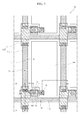
- trenches tch are formed in an insulation substrate 110 as a base of an array substrate 101.
- the trenches tch are located at a region where a gate line 113 and a gate electrode 117 are formed, and a part, except for a crossing part of the gate line 113 and the data line 130 and a part to a predetermined distance from the crossing portion, out of a region where a data line 130 is formed.
- the trench tch may have a depth of about 0.5 to 5 ⁇ m, and the trenches tch for the gate line 113 and the data line 130 may have respective widths which a gate line or data line of a common array substrate has.
- the gate line 113, the gate electrode 117 and a data pattern 115 fill the respective trenches tch.
- the gate line 113, the gate electrode 117 and the data pattern 115 may have a single-layered structure made of the same material, for example, one of aluminum (Al), aluminum alloy (e.g., AlNd), copper (Cu) and copper alloy.
- the data pattern 115 is located between adjacent gate lines 113.
- the gate line 113, the gate electrode 117 and the data pattern 115 may have a thickness which is the same as the depth of the trench tch. Accordingly, the surface of the gate line 113, the gate electrode 117 and a data pattern 115 may be substantially even with respect to the surface of the substrate 110.
- the gate line 113, the gate electrode 117 and the data pattern 115 have a thickness much greater than that of the gate line and the data line the related art, a step portion protruding upward from the surface of the substrate 110 is hardly formed. Thus, components to be formed later are not substantially affected by the gate line 113, the gate electrode 117 and the data pattern 115.
- a gate insulating layer 120 is formed on the entire surface of the substrate 110 having the gate line 113, the gate electrode 117 and the data pattern 115 therein.
- the gate insulating layer 120 may be made of an inorganic insulating material, for example, silicon oxide (SiO 2 ) or silicon nitride (SiNx).
- the gate insulating layer 120 is substantially even because the surface of the substrate therebelow having the gate line 113, the gate electrode 117 and the data pattern 115 is substantially even.
- the gate insulating layer 120 has first contact holes ch1 exposing ends of the data pattern 115.
- a semiconductor layer 125 is formed on the gate insulating layer in the switching region TrA corresponding to the gate electrode 117.
- the semiconductor layer 125 includes an active layer 125a made of intrinsic amorphous silicon, and an ohmic contact layer 125b made of impurity-doped amorphous silicon exposing a center portion of the active layer 125a.
- a data connection portion 131, and source and drain electrodes 133 and 136 are formed on the gate insulating layer 120 and the semiconductor layer 125.
- the data connection portion 131, and the source and drain electrodes 133 and 136 may have a single-layered or multi-layered structure using at least one of aluminum (Al), aluminum alloy (e.g., AlNd), copper (Cu), copper alloy, molybdenum (Mo), and molybdenum alloy (e.g., MoTi).
- the data connection portion 131 may be a data connection pattern, for example.
- the data connection portion 131 overlap the adjacent data patterns 115 at both sides thereof and the gate line 113, and contacts the data patterns 115 at both sides thereof through the first contact holes ch1.
- the source electrode 133 is connected to the data connection portion 131. More particularly, the source electrode 133 extends from the data connection portion 131 and is located on the ohmic contact layer 125b.
- the drain electrode 136 is spaced apart from the source electrode 133 and located on the ohmic contact layer 125b.
- the data patterns 115 formed at the trenches tch and the data connection portion 131 form the data line 130 extending along a direction crossing the gate line 113.
- the gate electrode 117, the gate insulating layer 120, the semiconductor layer 125, and the source and drain electrodes 133 and 136 form the thin film transistor Tr.
- a passivation layer is formed on the data connection portion 131 and the source and drain electrodes 133 and 136.
- the passivation layer includes a drain contact hole 148 exposing the drain electrode 136.
- the passivation layer may a single-layered structure using inorganic insulating material or organic insulating material, or a double-layered structure made using inorganic insulating material and organic insulating material.
- the passivation layer has a double-layered structure with a first layer 140 made of inorganic insulating material, and a second layer 145 made of organic insulating material and thus having an even surface.
- the active layer 125a contacts organic insulating material, a channel portion of the active layer 125a is contaminated by the organic insulating material, and thus property of the thin film transistor Tr may be degraded.
- the first layer 140 of inorganic insulating material is first formed and then the second layer 145 of organic insulating material is formed thereon.
- the second layer 145 of organic insulating material may be advantageous to operation of particular LCDs.
- the in-plane switching mode LCD and fringe field mode LCD prefer a pixel electrode formed on an flat surface for uniformity and efficiency of production of electric field, and in consideration of this, the second layer 145 is employed to produce a flat surface.
- a pixel electrode 150 is formed on the second layer 145 and contacts the drain electrode 136 through the drain contact hole 148.
- the pixel electrode 150 may be made of a transparent conductive material, for example, indium-tin-oxide (ITO) or indium-zinc-oxide (IZO).
- the passivation layer can be omitted.
- the pixel electrode 150 can be formed on, e.g., drain electrode 136 and connected to the drain electrode 136.
- the pixel electrode 150 may have a plate shape in the pixel region P, and in this case, the array substrate 110 may be used as an array substrate for a twist nematic mode LCD.
- the pixel electrode 150 may have other shapes according to the modes of LCDs.
- the pixel electrode 150 may be configured to have a plurality of bars spaced apart from one another, and a common electrode may be configured to have a plurality of another bars alternating with the bars of the pixel electrode 150 to produce an in-plane electric field.
- the common electrode is connected to a common line, and the common line may be formed in the substrate 110 filling a corresponding trench that is spaced apart from and parallel with the gate line 113.
- the pixel electrode 150 may be configured to have a plate shape, and a common electrode may be configured to have a plurality of bar-shaped openings to produce an in-plane electric field.
- the common electrode may be formed over the pixel electrode 150 with an insulating layer therebetween.
- the array substrate 101 can use the gate line 113 and the data line 130 several times to tens of times thicker than those of the related art. Accordingly, even when display area increases and the signal line becomes longer, thickness increases and thus resistance is reduced. Therefore, signal delay can be prevented.
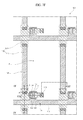
- FIG. 6 is a cross-sectional view illustrating an array substrate of an LCD according to a second embodiment of the present invention.
- the array substrate 202 of the second embodiment is similar to the array substrate 101 of the first embodiment but is different in the trench tch. Explanation of parts similar to parts of the first embodiment may be omitted.
- the trench tch of the first embodiment is formed in the substrate 110 while the trench tch of the second embodiment is formed in a buffer layer 112 on the substrate 110.
- the buffer layer 112 may be made of inorganic or organic insulating material.
- a gate line 113, a gate electrode 117 and a data pattern 115 fill the corresponding trenches tch in the buffer layer 112.
- the surface of the gate line 113, the gate electrode 117 and the data pattern 115 may be substantially even with respect to the surface of the buffer layer 112.
- the trench tch may be configured to open the surface of the substrate 110 therebelow.
- the trench tch may be configured to have a depth less than a thickness of the buffer layer 112.
- the layered structure over the gate line 113, the gate electrode 117 and the data pattern 115 is similar to that of the first embodiment.
- the array substrate 201 of the second embodiment can have the same advantages as that of the first embodiment 101.
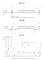
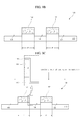
- FIGs. 7A to 7G are plan views illustrating a method of the array substrate of the LCD according to the first embodiment
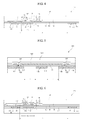
- FIGs. 8A to 8K are cross-sectional views taken along a line VIII-VIII of FIGs. 7A to 7G
- FIGs. 9A to 9K are cross-sectional views taken along a line IX-IX of FIGs. 7A to 7G .
- a first photoresist layer is formed on a substrate 110 which is made of, for example, glass or plastic, and then light exposure and developing are performed to form a first photoresist pattern 181 at regions except for regions where a gate line 113, a gate electrode 117 and a data pattern 115 are formed.
- the first photoresist pattern 181 exposes the regions where the gate line 113, the gate electrode 117 and the data pattern 115 are formed.
- the substrate 110 is etched using the first photoresist pattern 181 to form trenches tch.
- the trench tch may have a width of about 5 ⁇ m to about 15 ⁇ m and a depth 0.5 ⁇ m to 5 ⁇ m.
- the trench tch corresponding to the gate line 113 extends without disconnection along a first direction that is an extension direction of the gate line 113.
- the trench tch corresponding to the data pattern 115 extends along a second direction crossing the first direction and is separated with respect to each trench tch for the gate line 113.
- a catalytic layer 185 is formed entirely on the substrate 110 having the first photoresist pattern 181.
- the catalytic layer 185 may be made of palladium (Pd) group material, and may be formed by coating Pd-Sn colloid or depositing Pd ion (e.g., Pd 2+ ).
- a stripping process is performed to remove the first photoresist layer 181.
- the catalytic layer 185 on the first photoresist pattern 181 is removed, and thus the catalytic layer 185 remains on an inner surface of the trench tch, and the surface of the substrate 110 outside the trench tch is exposed without the catalytic layer 185 thereon.
- the substrate 110 having the catalytic layer 185 in the trench tch is immersed in a tank 195 containing a plating solution in which at least one metal material of low resistance, for example, at least one of aluminum (Al), aluminum alloy, copper and copper alloy ion is dissolved, and electroless plating is performed.
- a plating solution in which at least one metal material of low resistance, for example, at least one of aluminum (Al), aluminum alloy, copper and copper alloy ion is dissolved, and electroless plating is performed.
- metal ion is selectively plated in the trench tch having the catalytic layer 185 therein but is not plated on the surface of the substrate 110 not having the catalytic layer 185.
- the gate line 113, the gate electrode 117 and the data pattern 115 are formed filling the corresponding trenches tch.
- a gate insulating layer 120 is formed entirely on the substrate 110 having the gate line 113, the gate electrode 117 and the data pattern 115.
- the gate insulating layer 120 may be made of inorganic insulating material, for example, silicon oxide (SiO 2 ) or silicon nitride (SiNx).
- the gate insulating layer 120 is substantially flat without a step portion on the substrate 110 because the surface of the gate line 113, the gate electrode 117 and the data pattern 115 below the gate insulating layer is substantially even with the surface of the substrate 110.
- intrinsic amorphous silicon layer and impurity-doped amorphous silicon layer are formed on the gate insulating layer 120, and then a mask process is performed to form an active layer 125a and an impurtity-doped amorphous silicon pattern 124 on the active layer 125a.
- a mask process is performed for the substrate 110 having the active layer 125a and the imputiry-doped amorphous silicon pattern 124 to remove portions of the gate insulating layer 120 corresponding to ends of the data pattern 115 and form a first contact hole ch1 exposing each of both ends of the data pattern 115.
- a second metal layer is formed on the substrate 110 having the first contact hole ch1.
- the second metal layer may be formed by depositing at least one from a metal material group including aluminum (Al), aluminum alloy, copper, copper alloy, molybdenum and molybdenum alloy.
- a mask process is performed for the second metal layer to form a data connection portion 131, and source and drain electrodes 133 and 136.
- the data connection portion 131 crosses the corresponding gate line 113, and contacts the data patterns 115 at both sides thereof through the respective first contact hole ch1 to connect the data patterns 115.
- the source electrode 133 branches off from the data connection portion 131, and the drain electrode 136 is spaced apart from the source electrode 133.
- the source and drain electrodes 133 and 136 are formed on the impurity-doped amorphous silicon pattern 124.
- the data pattern 115 and the data connection portion 131 are alternated and connected along the second direction to form each data line 130.
- a portion of the impurity-doped amorphous silicon pattern 124 exposed between the source and drain electrodes 133 and 136 are removed to form an ohmic contact layer 125b below each of the source and drain electrodes 133 and 136 and expose a center portion of the active layer 125a.
- the active layer 125a and the ohmic contact layer 125b form a semiconductor layer 125.
- the gate electrode 117, the gate insulating layer 120, the semiconductor layer 125 and the source and drain electrodes 133 and 136 in the switching region TrA form a thin film transistor Tr.
- a first passivation layer 140 is formed on the substrate 110 having the source and drain electrodes 133 and 136, and then a second passivation layer 145 is formed on the first passivation layer 140.
- the first passivation layer 140 may be made of inorganic insulating material, for example, silicon oxide (SiO 2 ) or silicon nitride (SiNx), and the second passivation layer 145 may be made of organic insulating material, for example, photo acryl.
- a mask process is performed for the first and second passivation layer 140 and 145 to form a drain contact hole 148 exposing the drain electrode 136.
- a transparent conductive material layer is formed on the second passivation layer 145 and patterned in a mask process to form a pixel electrode 150 in the pixel region P.
- the pixel electrode 150 contacts the drain electrode 136 through the drain contact hole 148.
- the passivation layers can be omitted.
- the transparent conductive material layer can be formed on, e.g., drain electrode 136 and patterned in a mask process to form a pixel electrode 150 in the pixel region P.
- the pixel electrode 150 is connected to the drain electrode 136.
- the array substrate 101 can be fabricated.
- the array substrate 101 as above may be used for a twisted nematic mode LCD.
- the pixel electrode 150 is formed to have a plurality of bars in the pixel region and a common electrode may be formed, in the same process of forming the pixel electrode 150, to have a plurality of another bars alternating with the bars of the pixel electrode 150.
- the array substrate 110 having such the configuration may be used for an in-plane switching mode LCD.
- a common line may be formed in the process of forming the gate line 113, a common contact hole may be formed in the process of forming the drain contact hole 148 of the passivation layers 140 and 145, and the common electrode may contact the common line through the common contact hole.
- an insulating layer is formed on the pixel electrode 150, and then a common electrode is formed on the insulating layer to have a plurality of bar-shaped openings over the pixel electrode 150.
- the array substrate 110 having such the configuration may be used for a fringe field mode LCD.
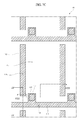
- FIGs. 10A to 10E are cross-sectional views illustrating a method of the array substrate of the LCD according to the second embodiment.
- the method of fabricating the array substrate of the second embodiment includes forming a trench in a buffer layer other than a substrate, and the processes after forming the trench in the buffer layer is similar to are similar to those of the first embodiment and explanations thereof may be omitted.
- a buffer layer 112 is formed on a substrate 110.
- the buffer layer 112 may be made of inorganic insulating material, for example, silicon oxide (SiO 2 ) or silicon nitride (SiNx), or organic insulating material, for example, photo acryl, polyimide or polystyrene.
- the buffer layer 112 may have a thickness equal to or more than that of a gate line 113, a gate electrode 117 and a data pattern 115 to be formed later.
- a photoresist layer is formed on the buffer layer 112 and patterned in a mask process to form a first photoresist pattern 181 at regions except for regions where the gate line 113, the gate electrode 117 and the data pattern 115 are formed.
- the first photoresist pattern 181 exposes the regions where the gate line 113, the gate electrode 117 and the data pattern 115 are formed.
- the buffer layer 112 is etched using the first photoresist pattern 181 as an etching mask to form a trench tch.
- the trench tch may have a depth about 0.5 ⁇ m to 5 ⁇ m.
- the trench tch may expose the substrate 110 by completely removing the buffer layer 112 or may not expose the substrate 110 by partially removing the buffer layer 112.
- a catalytic layer 185 is formed entirely on the first photoresist pattern 181 and in the trench tch.
- the catalytic layer 185 may be made of palladium (Pd) group material, and may be formed by coating Pd-Sn colloid or depositing Pd ion (e.g., Pd 2+ ).
- a stripping process is performed to remove the first photoresist layer 181.
- the catalytic layer 185 on the first photoresist pattern 181 is removed, and thus the catalytic layer 185 remains on an inner surface of the trench tch, and the surface of the buffer layer 112 outside the trench tch is exposed without the catalytic layer 185 thereon.
- the substrate 110 having the catalytic layer 185 in the trench tch is immersed in a tank 195 containing a plating solution in which at least one metal material of low resistance, for example, at least one of aluminum (Al), aluminum alloy, copper and copper alloy ion is dissolved, and electroless plating is performed.
- a plating solution in which at least one metal material of low resistance, for example, at least one of aluminum (Al), aluminum alloy, copper and copper alloy ion is dissolved, and electroless plating is performed.
- metal ion is selectively plated in the trench tch having the catalytic layer 185 therein but is not plated on the surface of the buffer layer 112 not having the catalytic layer 185.
- the gate line 113, the gate electrode 117 and the data pattern 115 are formed filling the corresponding trenches tch.
- the post processes may be described with reference to the method of the first embodiment.
- the array substrate 101 can use the gate line and the data line several times to tens of times thicker than those of the related art. Accordingly, even when display area increases and the signal line becomes longer, thickness increases and thus resistance is reduced. Therefore, signal delay can be prevented.
Landscapes
- Physics & Mathematics (AREA)
- Nonlinear Science (AREA)
- Engineering & Computer Science (AREA)
- Mathematical Physics (AREA)
- Chemical & Material Sciences (AREA)
- Crystallography & Structural Chemistry (AREA)
- Microelectronics & Electronic Packaging (AREA)
- General Physics & Mathematics (AREA)
- Optics & Photonics (AREA)
- Liquid Crystal (AREA)
- Thin Film Transistor (AREA)
- Devices For Indicating Variable Information By Combining Individual Elements (AREA)
- Manufacturing & Machinery (AREA)
Abstract
Description
- The present invention claims the benefit of Korean Patent Application No.
10-2013-0075901 - The present invention relates to an array substrate for a liquid crystal display, and more particularly, to an array substrate for a liquid crystal display and a method of fabricating the same.
- Recently, with the advent of an information-oriented society, the field of display devices configured to process and display a large amount of information has rapidly been developed. In particular, liquid crystal displays (LCDs) or organic light emitting diodes (OLEDs) have lately been developed as flat panel displays (FPDs) having excellent performance, such as a small thickness, light weight, and low power consumption, and has superseded conventional cathode-ray tubes (CRTs).
- Among LCDs, an active matrix (AM)-type LCD including an array substrate having a TFT serving as a switching element capable of controlling on/off voltages of each of pixels may have excellent resolution and capability of embodying moving images.
- Generally, the LCD is fabricated by fabricating an array substrate and a color filter substrate and interposing a liquid crystal layer between the array substrate and the color filter substrate.
-
FIG. 1 is an exploded perspective view illustrating an LCD or an OLED according to the related art. - Referring to
FIG. 1 , anarray substrate 10 and acolor filter substrate 20 is attached to each other with aliquid crystal layer 30 therebetween. Thearray substrate 10 includes a plurality ofgate lines 14 and a plurality ofdata lines 16 to define a plurality of pixel regions P on afirst substrate 12. A thin film transistor T is formed at the crossing portion of the gate anddata lines pixel electrode 18 in the pixel region P. - The
color filter substrate 20 includes a black matrix 25 corresponding to the gate anddata lines color filter layer 26 including red (R), green (G) and blue (B) 26a, 26b and 26c arranged in the respective pixel regions P, and acommon electrode 28 on the black matrix 25 and thecolor filter layer 26. - Although not shown in the drawings, a sealant is formed between the
array substrate 10 and thecolor filter substrate 20 to prevent leakage of liquid crystal, alignment layers are formed on inner surfaces of thearray substrate 10 and thecolor filter substrate 20, respectively, and polarizers are located on outer surfaces of thearray substrate 10 and thecolor filter substrate 20, respectively. - Moreover, a backlight unit is provided below the
array substrate 10. A gate signal is sequentially supplied to thegate lines 14, then the corresponding thin film transistor T is turned on and a data signal is supplied to thedata line 16 and then to thepixel electrode 18, and thus an electric field is produced between thepixel electrode 18 and thecommon electrode 28 to operate liquid crystal molecules of theliquid crystal layer 30, thereby displaying images. -
FIG. 2 is a cross-sectional view illustrating an array substrate according to the related art. - Referring to
FIG. 2 , in thearray substrate 10, a gate line (not shown) and adata line 16 cross each other to define a pixel region P, and agate electrode 55 is formed in a switching region TrA of the pixel region P on afirst substrate 11. - A
gate insulating layer 58 is formed on the gate electrode 50, and asemiconductor layer 68 including anactive layer 62 made of intrinsic amorphous silicon and anohmic contact layer 66 made of impurity-doped amorphous silicon is formed on thegate insulating layer 58. - Source and
drain electrodes ohmic contact layer 66. Thegate electrode 55, thegate insulating layer 58, thesemiconductor layer 68 and the source anddrain electrodes - A
passivation layer 82 is on the source anddrain electrodes drain contact hole 85 exposing thedrain electrode 78. Apixel electrode 18 is formed on thepassivation layer 82 in the pixel region P contacts thedrain electrode 78 through thedrain contact hole 85. - The gate line has predetermined thickness and width, and the
data line 16 has predetermined thickness and width. - As size of the LCD increases, the gate line and the data line become longer. This causes increase of resistance of signal line, and thus signal delay occurs. Accordingly, signal deformation and operation defect are caused, and display quality is degraded.
- To prevent such the signal delay, signal line is required to increase in thickness and/or width. However, in case of increase in width, aperture ratio is reduced. In case of increase in thickness, step portion becomes great, and this causes disconnection of a component over the signal line. Moreover, such the step portion causes vacant space at sides of the signal line, insulation capability is thus degraded, and thus short-circuit between the signal line and a conductive component to be formed later may occur.
- Accordingly, the present invention is directed to an array substrate for an LCD and a method of fabricating the same which substantially obviates one or more of the problems due to limitations and disadvantages of the related art.
- An advantage of the present invention is to provide an array substrate for an LCD and a method of fabricating the same that can reduce signal delay and step portion with increase of thickness of signal line.
- Additional features and advantages of the present invention will be set forth in the description which follows, and in part will be apparent from the description, or may be learned by practice of the invention. These and other advantages of the invention will be realized and attained by the structure particularly pointed out in the written description and claims thereof as well as the appended drawings.
- To achieve these and other advantages and in accordance with the purpose of the present invention, as embodied and broadly described herein, an array substrate includes: a layer arrangement including a pixel region; a trench having a depth from a surface of the layer arrangement; a gate line, a gate electrode and a data pattern filling the respective trenches, wherein the data pattern is between the adjacent gate lines; a gate insulating layer on the gate line, the gate electrode and the data pattern, substantially flat over the layer arrangement, and including contact holes that expose both ends of the data pattern, respectively; a semiconductor layer on the gate insulating layer over the gate electrode; a data connection portion on the gate insulating layer and contacting the adjacent data patterns through the contact holes; a source electrode connected to the data connection portion, and a drain electrode spaced apart from the source electrode; a pixel electrode connected to the drain electrode.
- In one or more embodiments, the layer arrangement comprises a substrate including the pixel region, wherein the surface of the layer arrangement is a surface of the substrate, and wherein the gate insulating layer is substantially flat over the substrate.
- In one or more embodiments, the layer arrangement comprises a substrate including the pixel region, and a buffer layer on the substrate, wherein the surface of the layer arrangement is a surface of the buffer layer, and wherein the gate insulating layer is substantially flat over the substrate.
- In one or more embodiments, the depth is equal to or less than a thickness of the buffer layer.
- In one or more embodiments, the array substrate further comprises: a passivation layer on the source and drain electrodes and including a drain contact hole exposing the drain electrode, wherein the pixel electrode is on the passivation layer and contacts the drain electrode through the drain contact hole, and wherein the source electrode extends from the data connection portion and on the semiconductor layer.
- In one or more embodiments, the depth is about 0.5 µm to about 5 µm, and the gate line, the gate electrode and the data pattern have a thickness equal to the depth.
- In another aspect, a method of fabricating an array substrate includes: providing a layer arrangement including a pixel region; etching the layer arrangement including the pixel region to form a trench having a depth from a surface of the layer arrangement; forming a gate line, a gate electrode and a data pattern filling the respective trenches, wherein the data pattern is between the adjacent gate lines; forming a gate insulating layer on the gate line, the gate electrode and the data pattern, the gate insulating layer being substantially flat over the layer arrangement; forming a semiconductor layer on the gate insulating layer over the gate electrode; patterning the gate insulating layer to form contact holes that expose both ends of the data pattern, respectively; forming a data connection portion on the gate insulating layer, the data connection portion contacting the adjacent data patterns through the contact holes, a source electrode connected to the data connection portion, and a drain electrode spaced apart from the source electrode; and forming a pixel electrode connected to the drain electrode.
- In one or more embodiments, providing the layer arrangement comprises providing a substrate including the pixel region, wherein etching the layer arrangement comprises etching the substrate including the pixel region to form the trench having the depth from a surface of the substrate, and wherein the gate insulating layer is substantially flat over the substrate.
- In one or more embodiments, etching the substrate including the pixel region to form the trench having the depth from the surface of the substrate, and forming the gate line, the gate electrode and the data pattern filling the respective trenches comprises: forming a photoresist pattern on the substrate and exposing a portion corresponding to the trench; etching the substrate using the photoresist pattern to form the trench; forming a catalytic layer on the trench and the photoresist pattern; removing the photoresist pattern, whereby the catalytic layer remains in the trench; and immersing the substrate having the catalytic layer remaining in the trench into a plating solution in which a metal material is dissolved and performing an electroless plating, thereby plating the metal material in the trench.
- In one or more embodiments, providing the layer arrangement comprises forming a buffer layer on a substrate including the pixel region, wherein etching the layer arrangement comprises etching the buffer layer to form the trench having the depth from a surface of the buffer layer, and wherein the gate insulating layer is substantially flat over the buffer layer.
- In one or more embodiments, etching the buffer layer to form the trench having the depth from the surface of the buffer layer, and forming the gate line, the gate electrode and the data pattern filling the respective trenches comprises: forming a photoresist pattern on the buffer layer which exposes a portion corresponding to the trench; etching the buffer layer using the photoresist pattern to form the trench; forming a catalytic layer on the trench and the photoresist pattern; removing the photoresist pattern, whereby the catalytic layer remains in the trench; and immersing the substrate having the catalytic layer remaining in the trench into a plating solution in which a metal material is dissolved and performing an electroless plating, thereby plating the metal material in the trench.
- In one or more embodiments, the depth is equal to or less than a thickness of the buffer layer.
- In one or more embodiments, the catalytic layer is formed by coating Pd-Sn colloid or depositing Pd ion.
- In one or more embodiments, the method further comprises: after forming a data connection portion on the gate insulating layer, forming a passivation layer on the source and drain electrodes, the passivation layer including a drain contact hole exposing the drain electrode, wherein the pixel electrode is on the passivation layer and contacts the drain electrode through the drain contact hole, and wherein the source electrode extends from the data connection portion and on the semiconductor layer.
- In one or more embodiments, the depth is 0.5 µm to 5 µm.
- In another aspect, an array substrate includes: a substrate including a pixel region; a trench having a depth from a surface of the substrate; a gate line, a gate electrode and a data pattern filling the respective trenches, wherein the data pattern is between the adjacent gate lines; a gate insulating layer on the gate line, the gate electrode and the data pattern, substantially flat over the substrate, and including contact holes that expose both ends of the data pattern, respectively; a semiconductor layer on the gate insulating layer over the gate electrode; a data connection portion on the gate insulating layer and contacting the adjacent data patterns through the contact holes; a source electrode connected to the data connection portion, and a drain electrode spaced apart from the source electrode; a pixel electrode connected to the drain electrode.
- In one or more embodiments, the array substrate further comprises: a passivation layer on the source and drain electrodes and including a drain contact hole exposing the drain electrode, wherein the pixel electrode is on the passivation layer and contacts the drain electrode through the drain contact hole, and wherein the source electrode extends from the data connection portion and on the semiconductor layer.
- In one or more embodiments, the depth is about 0.5 µm to about 5 µm, and the gate line, the gate electrode and the data pattern have a thickness equal to the depth.
- In another aspect, an array substrate includes: a substrate including a pixel region; a buffer layer on the substrate and including a trench having a depth from a surface of the buffer layer; a gate line, a gate electrode and a data pattern filling the respective trenches, wherein the data pattern is between the adjacent gate lines; a gate insulating layer on the gate line, the gate electrode and the data pattern, substantially flat over the substrate, and including contact holes that expose both ends of the data pattern, respectively; a semiconductor layer on the gate insulating layer over the gate electrode; a data connection portion on the gate insulating layer and contacting the adjacent data patterns through the contact holes; a source electrode connected to the data connection portion, and a drain electrode spaced apart from the source electrode; a pixel electrode connected to the drain electrode.
- In one or more embodiments, the array substrate further comprises: a passivation layer on the source and drain electrodes and including a drain contact hole exposing the drain electrode, wherein the pixel electrode is on the passivation layer and contacts the drain electrode through the drain contact hole, and wherein the source electrode extends from the data connection portion and on the semiconductor layer.
- In one or more embodiments, the depth is 0.5 µm to 5 µm, and the gate line, the gate electrode and the data pattern have a thickness that is the same as the depth.
- In one or more embodiments, the depth is equal to or less than a thickness of the buffer layer.
- In another aspect, a method of fabricating an array substrate includes: etching a substrate including a pixel region to form a trench having a depth from a surface of the substrate; forming a gate line, a gate electrode and a data pattern filling the respective trenches, wherein the data pattern is between the adjacent gate lines; forming a gate insulating layer on the gate line, the gate electrode and the data pattern, the gate insulating layer being substantially flat over the substrate; forming a semiconductor layer on the gate insulating layer over the gate electrode; patterning the gate insulating layer to form contact holes that expose both ends of the data pattern, respectively; forming a data connection portion on the gate insulating layer, the data connection portion contacting the adjacent data patterns through the contact holes, a source electrode connected to the data connection portion, and a drain electrode spaced apart from the source electrode; and forming a pixel electrode connected to the drain electrode.
- In one or more embodiments, the method further comprises: after forming a data connection portion on the gate insulating layer, forming a passivation layer on the source and drain electrodes, the passivation layer including a drain contact hole exposing the drain electrode, wherein the pixel electrode is on the passivation layer and contacts the drain electrode through the drain contact hole, and wherein the source electrode extends from the data connection portion and on the semiconductor layer.
- In one or more embodiments, etching the substrate including the pixel region to form the trench having the depth from a surface of the substrate, and forming the gate line, the gate electrode and the data pattern filling the respective trenches comprises: forming a photoresist pattern on the substrate and exposing a portion corresponding to the trench; etching the substrate using the photoresist pattern to form the trench; forming a catalytic layer on the trench and the photoresist pattern; removing the photoresist pattern, whereby the catalytic layer remains in the trench; and immersing the substrate having the catalytic layer remaining in the trench into a plating solution in which a metal material is dissolved and performing an electroless plating, thereby plating the metal material in the trench.
- In one or more embodiments, the depth is 0.5 µm to 5 µm.
- In one or more embodiments, the catalytic layer is formed by coating Pd-Sn colloid or depositing Pd ion.
- In another aspect, a method of fabricating an array substrate comprises: forming a buffer layer on a substrate including a pixel region; etching the buffer layer to form a trench having a depth from a surface of the buffer layer; forming a gate line, a gate electrode and a data pattern filling the respective trenches, wherein the data pattern is between the adjacent gate lines; forming a gate insulating layer on the gate line, the gate electrode and the data pattern, and substantially flat over the substrate; forming a semiconductor layer on the gate insulating layer over the gate electrode; patterning the gate insulating layer to form contact holes that expose both ends of the data pattern, respectively; forming a data connection portion on the gate insulating layer, which contacts the adjacent data patterns through the contact holes, a source electrode connected to the data connection portion, and a drain electrode spaced apart from the source electrode; and forming a pixel electrode connected to the drain electrode.
- In one or more embodiments, the method further comprises: after forming a data connection portion on the gate insulating layer, forming a passivation layer on the source and drain electrodes, the passivation layer including a drain contact hole exposing the drain electrode, wherein the pixel electrode is on the passivation layer and contacts the drain electrode through the drain contact hole, and wherein the source electrode extends from the data connection portion and on the semiconductor layer.
- In one or more embodiments, etching the buffer layer to form the trench having the depth from a surface of the buffer layer, and forming the gate line, the gate electrode and the data pattern filling the respective trenches comprises: forming a photoresist pattern on the buffer layer which exposes a portion corresponding to the trench; etching the buffer layer using the photoresist pattern to form the trench; forming a catalytic layer on the trench and the photoresist pattern; removing the photoresist pattern, whereby the catalytic layer remains in the trench; and immersing the substrate having the catalytic layer remaining in the trench into a plating solution in which a metal material is dissolved and performing an electroless plating, thereby plating the metal material in the trench.
- In one or more embodiments, the depth is equal to or less than a thickness of the buffer layer.
- In one or more embodiments, the depth is 0.5 µm to 5 µm.
- In one or more embodiments, the catalytic layer is formed by coating Pd-Sn colloid or depositing Pd ion.
- In another aspect, an array substrate includes: a substrate including a pixel region; a trench having a depth from a surface of the substrate; a gate line, a gate electrode and a data pattern filling the respective trenches, wherein the data pattern is between the adjacent gate lines; a gate insulating layer on the gate line, the gate electrode and the data pattern, substantially flat over the substrate, and including contact holes that expose both ends of the data pattern, respectively; a semiconductor layer on the gate insulating layer over the gate electrode; a data connection portion on the gate insulating layer and contacting the adjacent data patterns through the contact holes; a source electrode extending from the data connection portion and on the semiconductor layer, and a drain electrode spaced apart from the source electrode; a passivation layer on the source and drain electrodes and including a drain contact hole exposing the drain electrode; and a pixel electrode on the passivation layer and contacting the drain electrode through the drain contact hole.
- In another aspect, an array substrate includes: a substrate including a pixel region; a buffer layer on the substrate and including a trench having a depth from a surface of the buffer layer; a gate line, a gate electrode and a data pattern filling the respective trenches, wherein the data pattern is between the adjacent gate lines; a gate insulating layer on the gate line, the gate electrode and the data pattern, substantially flat over the substrate, and including contact holes that expose both ends of the data pattern, respectively; a semiconductor layer on the gate insulating layer over the gate electrode; a data connection portion on the gate insulating layer and contacting the adjacent data patterns through the contact holes; a source electrode extending from the data connection portion and on the semiconductor layer, and a drain electrode spaced apart from the source electrode; a passivation layer on the source and drain electrodes and including a drain contact hole exposing the drain electrode; and a pixel electrode on the passivation layer and contacting the drain electrode through the drain contact hole.
- In yet another aspect, a method of fabricating an array substrate includes: etching a substrate including a pixel region to form a trench having a depth from a surface of the substrate; forming a gate line, a gate electrode and a data pattern filling the respective trenches, wherein the data pattern is between the adjacent gate lines; forming a gate insulating layer on the gate line, the gate electrode and the data pattern, and the gate insulating layer being substantially flat over the substrate; forming a semiconductor layer on the gate insulating layer over the gate electrode; patterning the gate insulating layer to form contact holes that expose both ends of the data pattern, respectively; forming a data connection portion on the gate insulating layer and contacting the adjacent data patterns through the contact holes, a source electrode extending from the data connection portion and on the semiconductor layer, and a drain electrode spaced apart from the source electrode; forming a passivation layer on the source and drain electrodes and including a drain contact hole exposing the drain electrode; and forming a pixel electrode on the passivation layer and contacting the drain electrode through the drain contact hole.
- In yet another aspect, a method of fabricating an array substrate includes: forming a buffer layer on a substrate including a pixel region; etching the buffer layer to form a trench having a depth from a surface of the buffer layer; forming a gate line, a gate electrode and a data pattern filling the respective trenches, wherein the data pattern is between the adjacent gate lines; forming a gate insulating layer on the gate line, the gate electrode and the data pattern, and substantially flat over the substrate; forming a semiconductor layer on the gate insulating layer over the gate electrode; patterning the gate insulating layer to form contact holes that expose both ends of the data pattern, respectively; forming a data connection portion on the gate insulating layer and contacting the adjacent data patterns through the contact holes, a source electrode extending from the data connection portion and on the semiconductor layer, and a drain electrode spaced apart from the source electrode; forming a passivation layer on the source and drain electrodes and including a drain contact hole exposing the drain electrode; and forming a pixel electrode on the passivation layer and contacting the drain electrode through the drain contact hole.
- It is to be understood that both the foregoing general description and the following detailed description are exemplary and explanatory and are intended to provide further explanation of the invention as claimed.
- The accompanying drawings, which are included to provide a further understanding of the invention and are incorporated in and constitute a part of this specification, illustrate embodiments of the invention and together with the description serve to explain the principles of the invention.
- In the drawings:
-
FIG. 1 is an exploded perspective view illustrating an LCD or an OLED according to the related art; -
FIG. 2 is a cross-sectional view illustrating an array substrate according to the related art; -
FIG. 3 is a plan view illustrating an array substrate of an LCD according to a first embodiment of the present invention; -
FIG. 4 is a cross-sectional view taken along a line, IV-IV ofFIG. 3 ; -
FIG. 5 is a cross-sectional view taken along a line, V-V ofFIG. 3 ; -
FIG. 6 is a cross-sectional view illustrating an array substrate of an LCD according to a second embodiment of the present invention; -
FIGs. 7A to 7G are plan views illustrating a method of fabricating the array substrate of the LCD according to the first embodiment; -
FIGs. 8A to 8K are cross-sectional views taken along a line VIII-VIII ofFIGs. 7A to 7G ; -
FIGs. 9A to 9K are cross-sectional views taken along a line IX-IX ofFIGs. 7A to 7G ; and -
FIGs. 10A to 10E are cross-sectional views illustrating a method of fabricating the array substrate of the LCD according to the second embodiment. - Reference will now be made in detail to the illustrated embodiments of the present invention, which are illustrated in the accompanying drawings.
-
FIG. 3 is a plan view illustrating an array substrate of an LCD according to a first embodiment of the present invention,FIG. 4 is a cross-sectional view taken along a line, IV-IV ofFIG. 3 , andFIG. 5 is a cross-sectional view taken along a line, V-V ofFIG. 3 . For the purpose of explanation, a region where a thin film transistor Tr as a switching element is formed in a pixel region P is referred to as a switching region TrA. - Referring to
FIGs. 3 to 5 , trenches tch are formed in aninsulation substrate 110 as a base of anarray substrate 101. For example, the trenches tch are located at a region where agate line 113 and agate electrode 117 are formed, and a part, except for a crossing part of thegate line 113 and thedata line 130 and a part to a predetermined distance from the crossing portion, out of a region where adata line 130 is formed. - It is preferred, but not required that the trench tch may have a depth of about 0.5 to 5 µm, and the trenches tch for the
gate line 113 and thedata line 130 may have respective widths which a gate line or data line of a common array substrate has. - In the
substrate 110, thegate line 113, thegate electrode 117 and adata pattern 115 fill the respective trenches tch. Thegate line 113, thegate electrode 117 and thedata pattern 115 may have a single-layered structure made of the same material, for example, one of aluminum (Al), aluminum alloy (e.g., AlNd), copper (Cu) and copper alloy. Thedata pattern 115 is located between adjacent gate lines 113. - The
gate line 113, thegate electrode 117 and thedata pattern 115 may have a thickness which is the same as the depth of the trench tch. Accordingly, the surface of thegate line 113, thegate electrode 117 and adata pattern 115 may be substantially even with respect to the surface of thesubstrate 110. - Accordingly, even when the
gate line 113, thegate electrode 117 and thedata pattern 115 have a thickness much greater than that of the gate line and the data line the related art, a step portion protruding upward from the surface of thesubstrate 110 is hardly formed. Thus, components to be formed later are not substantially affected by thegate line 113, thegate electrode 117 and thedata pattern 115. - A
gate insulating layer 120 is formed on the entire surface of thesubstrate 110 having thegate line 113, thegate electrode 117 and thedata pattern 115 therein. Thegate insulating layer 120 may be made of an inorganic insulating material, for example, silicon oxide (SiO2) or silicon nitride (SiNx). - The
gate insulating layer 120 is substantially even because the surface of the substrate therebelow having thegate line 113, thegate electrode 117 and thedata pattern 115 is substantially even. Thegate insulating layer 120 has first contact holes ch1 exposing ends of thedata pattern 115. - A
semiconductor layer 125 is formed on the gate insulating layer in the switching region TrA corresponding to thegate electrode 117. - The
semiconductor layer 125 includes anactive layer 125a made of intrinsic amorphous silicon, and anohmic contact layer 125b made of impurity-doped amorphous silicon exposing a center portion of theactive layer 125a. - A
data connection portion 131, and source and drainelectrodes gate insulating layer 120 and thesemiconductor layer 125. Thedata connection portion 131, and the source and drainelectrodes data connection portion 131 may be a data connection pattern, for example. Thedata connection portion 131 overlap theadjacent data patterns 115 at both sides thereof and thegate line 113, and contacts thedata patterns 115 at both sides thereof through the first contact holes ch1. Thesource electrode 133 is connected to thedata connection portion 131. More particularly, thesource electrode 133 extends from thedata connection portion 131 and is located on theohmic contact layer 125b. Thedrain electrode 136 is spaced apart from thesource electrode 133 and located on theohmic contact layer 125b. - The
data patterns 115 formed at the trenches tch and thedata connection portion 131 form thedata line 130 extending along a direction crossing thegate line 113. - The
gate electrode 117, thegate insulating layer 120, thesemiconductor layer 125, and the source and drainelectrodes - A passivation layer is formed on the
data connection portion 131 and the source and drainelectrodes drain contact hole 148 exposing thedrain electrode 136. - The passivation layer may a single-layered structure using inorganic insulating material or organic insulating material, or a double-layered structure made using inorganic insulating material and organic insulating material. In this embodiment, for the purpose of explanation, the passivation layer has a double-layered structure with a
first layer 140 made of inorganic insulating material, and asecond layer 145 made of organic insulating material and thus having an even surface. - In this regard, when the
active layer 125a contacts organic insulating material, a channel portion of theactive layer 125a is contaminated by the organic insulating material, and thus property of the thin film transistor Tr may be degraded. To prevent this problem, thefirst layer 140 of inorganic insulating material is first formed and then thesecond layer 145 of organic insulating material is formed thereon. - Further, using the
second layer 145 of organic insulating material may be advantageous to operation of particular LCDs. In this regard, among various modes of LCDs such as twist nematic mode, in-plane switching mode, fringe field mode, etc., the in-plane switching mode LCD and fringe field mode LCD prefer a pixel electrode formed on an flat surface for uniformity and efficiency of production of electric field, and in consideration of this, thesecond layer 145 is employed to produce a flat surface. - A
pixel electrode 150 is formed on thesecond layer 145 and contacts thedrain electrode 136 through thedrain contact hole 148. Thepixel electrode 150 may be made of a transparent conductive material, for example, indium-tin-oxide (ITO) or indium-zinc-oxide (IZO). - However, the passivation layer can be omitted. And in this case, the
pixel electrode 150 can be formed on, e.g.,drain electrode 136 and connected to thedrain electrode 136. - The
pixel electrode 150 may have a plate shape in the pixel region P, and in this case, thearray substrate 110 may be used as an array substrate for a twist nematic mode LCD. - However, the
pixel electrode 150 may have other shapes according to the modes of LCDs. For example, in case that thearray substrate 101 is used for an in-plane switching mode LCD, thepixel electrode 150 may be configured to have a plurality of bars spaced apart from one another, and a common electrode may be configured to have a plurality of another bars alternating with the bars of thepixel electrode 150 to produce an in-plane electric field. In this case, the common electrode is connected to a common line, and the common line may be formed in thesubstrate 110 filling a corresponding trench that is spaced apart from and parallel with thegate line 113. - Alternatively, in case that the
array substrate 110 is used for a fringe field mode LCD, thepixel electrode 150 may be configured to have a plate shape, and a common electrode may be configured to have a plurality of bar-shaped openings to produce an in-plane electric field. In this case, the common electrode may be formed over thepixel electrode 150 with an insulating layer therebetween. - As described above, because of the trench tch, the
array substrate 101 can use thegate line 113 and thedata line 130 several times to tens of times thicker than those of the related art. Accordingly, even when display area increases and the signal line becomes longer, thickness increases and thus resistance is reduced. Therefore, signal delay can be prevented. - Moreover, even when the thickness of the
gate line 113 and thedata line 130 increases, a step portion due to this is not produced. Accordingly, disconnection of a component over the signal line or a vacant space near the signal line due to the step portion is prevented. Therefore, product defect rate and production cost can be reduced. -
FIG. 6 is a cross-sectional view illustrating an array substrate of an LCD according to a second embodiment of the present invention. - The array substrate 202 of the second embodiment is similar to the
array substrate 101 of the first embodiment but is different in the trench tch. Explanation of parts similar to parts of the first embodiment may be omitted. - The trench tch of the first embodiment is formed in the
substrate 110 while the trench tch of the second embodiment is formed in abuffer layer 112 on thesubstrate 110. Thebuffer layer 112 may be made of inorganic or organic insulating material. - A
gate line 113, agate electrode 117 and adata pattern 115 fill the corresponding trenches tch in thebuffer layer 112. The surface of thegate line 113, thegate electrode 117 and thedata pattern 115 may be substantially even with respect to the surface of thebuffer layer 112. - The trench tch may be configured to open the surface of the
substrate 110 therebelow. Alternatively, the trench tch may be configured to have a depth less than a thickness of thebuffer layer 112. - The layered structure over the
gate line 113, thegate electrode 117 and thedata pattern 115 is similar to that of the first embodiment. - The
array substrate 201 of the second embodiment can have the same advantages as that of thefirst embodiment 101. - Methods of fabricating the array substrates according to the first and second embodiments are explained as below.
-
FIGs. 7A to 7G are plan views illustrating a method of the array substrate of the LCD according to the first embodiment,FIGs. 8A to 8K are cross-sectional views taken along a line VIII-VIII ofFIGs. 7A to 7G , andFIGs. 9A to 9K are cross-sectional views taken along a line IX-IX ofFIGs. 7A to 7G . - Referring to
FIGs. 7A ,8A and9A , a first photoresist layer is formed on asubstrate 110 which is made of, for example, glass or plastic, and then light exposure and developing are performed to form afirst photoresist pattern 181 at regions except for regions where agate line 113, agate electrode 117 and adata pattern 115 are formed. In other words, thefirst photoresist pattern 181 exposes the regions where thegate line 113, thegate electrode 117 and thedata pattern 115 are formed. - Referring to
FIGs. 7A ,8B and9B , thesubstrate 110 is etched using thefirst photoresist pattern 181 to form trenches tch. The trench tch may have a width of about 5 µm to about 15 µm and a depth 0.5 µm to 5 µm. - The trench tch corresponding to the
gate line 113 extends without disconnection along a first direction that is an extension direction of thegate line 113. The trench tch corresponding to thedata pattern 115 extends along a second direction crossing the first direction and is separated with respect to each trench tch for thegate line 113. - Referring to
FIGs. 7A ,8C and9C , acatalytic layer 185 is formed entirely on thesubstrate 110 having thefirst photoresist pattern 181. For example, thecatalytic layer 185 may be made of palladium (Pd) group material, and may be formed by coating Pd-Sn colloid or depositing Pd ion (e.g., Pd2+). - Referring to
FIGs. 7A ,8D and9D , a stripping process is performed to remove thefirst photoresist layer 181. - Accordingly, the
catalytic layer 185 on thefirst photoresist pattern 181 is removed, and thus thecatalytic layer 185 remains on an inner surface of the trench tch, and the surface of thesubstrate 110 outside the trench tch is exposed without thecatalytic layer 185 thereon. - Referring to
FIGs. 7B ,8E and9E , thesubstrate 110 having thecatalytic layer 185 in the trench tch is immersed in atank 195 containing a plating solution in which at least one metal material of low resistance, for example, at least one of aluminum (Al), aluminum alloy, copper and copper alloy ion is dissolved, and electroless plating is performed. - Through the electroless plating, metal ion is selectively plated in the trench tch having the
catalytic layer 185 therein but is not plated on the surface of thesubstrate 110 not having thecatalytic layer 185. - Accordingly, when the electroless plating is finished, the
gate line 113, thegate electrode 117 and thedata pattern 115 are formed filling the corresponding trenches tch. - Referring to
FIGs. 7B ,8F and9F , agate insulating layer 120 is formed entirely on thesubstrate 110 having thegate line 113, thegate electrode 117 and thedata pattern 115. Thegate insulating layer 120 may be made of inorganic insulating material, for example, silicon oxide (SiO2) or silicon nitride (SiNx). - The
gate insulating layer 120 is substantially flat without a step portion on thesubstrate 110 because the surface of thegate line 113, thegate electrode 117 and thedata pattern 115 below the gate insulating layer is substantially even with the surface of thesubstrate 110. - Referring to
FIGs. 7C ,8G and9G , intrinsic amorphous silicon layer and impurity-doped amorphous silicon layer are formed on thegate insulating layer 120, and then a mask process is performed to form anactive layer 125a and an impurtity-dopedamorphous silicon pattern 124 on theactive layer 125a. - Referring to
FIGs. 7D ,8H and9H , a mask process is performed for thesubstrate 110 having theactive layer 125a and the imputiry-dopedamorphous silicon pattern 124 to remove portions of thegate insulating layer 120 corresponding to ends of thedata pattern 115 and form a first contact hole ch1 exposing each of both ends of thedata pattern 115. - Referring to
FIG. 7E ,8I and9I , a second metal layer is formed on thesubstrate 110 having the first contact hole ch1. The second metal layer may be formed by depositing at least one from a metal material group including aluminum (Al), aluminum alloy, copper, copper alloy, molybdenum and molybdenum alloy. - A mask process is performed for the second metal layer to form a
data connection portion 131, and source and drainelectrodes data connection portion 131 crosses thecorresponding gate line 113, and contacts thedata patterns 115 at both sides thereof through the respective first contact hole ch1 to connect thedata patterns 115. The source electrode 133 branches off from thedata connection portion 131, and thedrain electrode 136 is spaced apart from thesource electrode 133. The source and drainelectrodes amorphous silicon pattern 124. - The
data pattern 115 and thedata connection portion 131 are alternated and connected along the second direction to form eachdata line 130. - Then, a portion of the impurity-doped
amorphous silicon pattern 124 exposed between the source and drainelectrodes ohmic contact layer 125b below each of the source and drainelectrodes active layer 125a. - The
active layer 125a and theohmic contact layer 125b form asemiconductor layer 125. Thegate electrode 117, thegate insulating layer 120, thesemiconductor layer 125 and the source and drainelectrodes - Referring to
FIGs. 7F ,8J and9J , afirst passivation layer 140 is formed on thesubstrate 110 having the source and drainelectrodes second passivation layer 145 is formed on thefirst passivation layer 140. Thefirst passivation layer 140 may be made of inorganic insulating material, for example, silicon oxide (SiO2) or silicon nitride (SiNx), and thesecond passivation layer 145 may be made of organic insulating material, for example, photo acryl. - A mask process is performed for the first and
second passivation layer drain contact hole 148 exposing thedrain electrode 136. - Referring to
FIGs. 7G ,8K and9K , a transparent conductive material layer is formed on thesecond passivation layer 145 and patterned in a mask process to form apixel electrode 150 in the pixel region P. Thepixel electrode 150 contacts thedrain electrode 136 through thedrain contact hole 148. - However, the passivation layers can be omitted. And in this case, the transparent conductive material layer can be formed on, e.g.,
drain electrode 136 and patterned in a mask process to form apixel electrode 150 in the pixel region P. Thepixel electrode 150 is connected to thedrain electrode 136. - Through the above-described processes, the
array substrate 101 can be fabricated. Thearray substrate 101 as above may be used for a twisted nematic mode LCD. - Alternatively, the
pixel electrode 150 is formed to have a plurality of bars in the pixel region and a common electrode may be formed, in the same process of forming thepixel electrode 150, to have a plurality of another bars alternating with the bars of thepixel electrode 150. Thearray substrate 110 having such the configuration may be used for an in-plane switching mode LCD. - In case of the
array substrate 110 for the in-plane switching mode LCD, a common line may be formed in the process of forming thegate line 113, a common contact hole may be formed in the process of forming thedrain contact hole 148 of the passivation layers 140 and 145, and the common electrode may contact the common line through the common contact hole. - Alternatively, after forming the
pixel electrode 150, then an insulating layer is formed on thepixel electrode 150, and then a common electrode is formed on the insulating layer to have a plurality of bar-shaped openings over thepixel electrode 150. Thearray substrate 110 having such the configuration may be used for a fringe field mode LCD. -
FIGs. 10A to 10E are cross-sectional views illustrating a method of the array substrate of the LCD according to the second embodiment. - The method of fabricating the array substrate of the second embodiment includes forming a trench in a buffer layer other than a substrate, and the processes after forming the trench in the buffer layer is similar to are similar to those of the first embodiment and explanations thereof may be omitted.
- Referring to
FIG. 10A , abuffer layer 112 is formed on asubstrate 110. Thebuffer layer 112 may be made of inorganic insulating material, for example, silicon oxide (SiO2) or silicon nitride (SiNx), or organic insulating material, for example, photo acryl, polyimide or polystyrene. - The
buffer layer 112 may have a thickness equal to or more than that of agate line 113, agate electrode 117 and adata pattern 115 to be formed later. - Then, a photoresist layer is formed on the
buffer layer 112 and patterned in a mask process to form afirst photoresist pattern 181 at regions except for regions where thegate line 113, thegate electrode 117 and thedata pattern 115 are formed. In other words, thefirst photoresist pattern 181 exposes the regions where thegate line 113, thegate electrode 117 and thedata pattern 115 are formed. - Referring to
FIG. 10B , thebuffer layer 112 is etched using thefirst photoresist pattern 181 as an etching mask to form a trench tch. The trench tch may have a depth about 0.5 µm to 5 µm. The trench tch may expose thesubstrate 110 by completely removing thebuffer layer 112 or may not expose thesubstrate 110 by partially removing thebuffer layer 112. - Referring to
FIG. 10C , acatalytic layer 185 is formed entirely on thefirst photoresist pattern 181 and in the trench tch. For example, thecatalytic layer 185 may be made of palladium (Pd) group material, and may be formed by coating Pd-Sn colloid or depositing Pd ion (e.g., Pd2+). - Referring to
FIG. 10D , a stripping process is performed to remove thefirst photoresist layer 181. - Accordingly, the
catalytic layer 185 on thefirst photoresist pattern 181 is removed, and thus thecatalytic layer 185 remains on an inner surface of the trench tch, and the surface of thebuffer layer 112 outside the trench tch is exposed without thecatalytic layer 185 thereon. - Referring to
FIGs. 10E , thesubstrate 110 having thecatalytic layer 185 in the trench tch is immersed in atank 195 containing a plating solution in which at least one metal material of low resistance, for example, at least one of aluminum (Al), aluminum alloy, copper and copper alloy ion is dissolved, and electroless plating is performed. - Through the electroless plating, metal ion is selectively plated in the trench tch having the
catalytic layer 185 therein but is not plated on the surface of thebuffer layer 112 not having thecatalytic layer 185. - Accordingly, when the electroless plating is finished, the
gate line 113, thegate electrode 117 and thedata pattern 115 are formed filling the corresponding trenches tch. - The post processes may be described with reference to the method of the first embodiment.
- As described above, because of the trench tch, the
array substrate 101 can use the gate line and the data line several times to tens of times thicker than those of the related art. Accordingly, even when display area increases and the signal line becomes longer, thickness increases and thus resistance is reduced. Therefore, signal delay can be prevented. - Moreover, even when the thickness of the gate line and the data line increases, a step portion due to this is not produced. Accordingly, disconnection of a component over the signal line or a vacant space near the signal line due to the step portion is prevented. Therefore, product defect rate and production cost can be reduced.
- It will be apparent to those skilled in the art that various modifications and variations can be made in the present invention without departing from the spirit or scope of the invention. Thus, it is intended that the present invention cover the modifications and variations of this invention provided they come within the scope of the appended claims and their equivalents.
Claims (15)
- An array substrate comprising:a layer arrangement including a pixel region;a trench having a depth from a surface of the layer arrangement;a gate line, a gate electrode and a data pattern filling the respective trenches, wherein the data pattern is between the adjacent gate lines;a gate insulating layer on the gate line, the gate electrode and the data pattern, substantially flat over the layer arrangement, and including contact holes that expose both ends of the data pattern, respectively;a semiconductor layer on the gate insulating layer over the gate electrode;a data connection portion on the gate insulating layer and contacting the adjacent data patterns through the contact holes;a source electrode connected to the data connection portion, and a drain electrode spaced apart from the source electrode;a pixel electrode connected to the drain electrode.
- The array substrate of claim 1, wherein the layer arrangement comprises a substrate including the pixel region,
wherein the surface of the layer arrangement is a surface of the substrate, and
wherein the gate insulating layer is substantially flat over the substrate. - The array substrate of claim 1, wherein the layer arrangement comprises a substrate including the pixel region, and a buffer layer on the substrate,
wherein the surface of the layer arrangement is a surface of the buffer layer, and
wherein the gate insulating layer is substantially flat over the substrate. - The array substrate according to claim 3, wherein the depth is equal to or less than a thickness of the buffer layer.
- The array substrate according to any one of claims 1 to 4, further comprising:a passivation layer on the source and drain electrodes and including a drain contact hole exposing the drain electrode,wherein the pixel electrode is on the passivation layer and contacts the drain electrode through the drain contact hole, andwherein the source electrode extends from the data connection portion and on the semiconductor layer.
- The array substrate according to any one of claims 1 to 5, wherein the depth is about 0.5 µm to about 5 µm, and the gate line, the gate electrode and the data pattern have a thickness equal to the depth.
- A method of fabricating an array substrate comprising:providing a layer arrangement including a pixel region;etching the layer arrangement including the pixel region to form a trench having a depth from a surface of the layer arrangement;forming a gate line, a gate electrode and a data pattern filling the respective trenches, wherein the data pattern is between the adjacent gate lines;forming a gate insulating layer on the gate line, the gate electrode and the data pattern, the gate insulating layer being substantially flat over the layer arrangement;forming a semiconductor layer on the gate insulating layer over the gate electrode;patterning the gate insulating layer to form contact holes that expose both ends of the data pattern, respectively;forming a data connection portion on the gate insulating layer, the data connection portion contacting the adjacent data patterns through the contact holes, a source electrode connected to the data connection portion, and a drain electrode spaced apart from the source electrode; andforming a pixel electrode connected to the drain electrode.
- The method of claim 7, wherein providing the layer arrangement comprises providing a substrate including the pixel region,
wherein etching the layer arrangement comprises etching the substrate including the pixel region to form the trench having the depth from a surface of the substrate, and
wherein the gate insulating layer is substantially flat over the substrate. - The method according to claim 8, wherein etching the substrate including the pixel region to form the trench having the depth from the surface of the substrate, and forming the gate line, the gate electrode and the data pattern filling the respective trenches comprises:forming a photoresist pattern on the substrate and exposing a portion corresponding to the trench;etching the substrate using the photoresist pattern to form the trench;forming a catalytic layer on the trench and the photoresist pattern;removing the photoresist pattern, whereby the catalytic layer remains in the trench; andimmersing the substrate having the catalytic layer remaining in the trench into a plating solution in which a metal material is dissolved and performing an electroless plating, thereby plating the metal material in the trench.
- The method of claim 7, wherein providing the layer arrangement comprises forming a buffer layer on a substrate including the pixel region,
wherein etching the layer arrangement comprises etching the buffer layer to form the trench having the depth from a surface of the buffer layer, and
wherein the gate insulating layer is substantially flat over the buffer layer. - The method according to claim 10, wherein etching the buffer layer to form the trench having the depth from the surface of the buffer layer, and forming the gate line, the gate electrode and the data pattern filling the respective trenches comprises:forming a photoresist pattern on the buffer layer which exposes a portion corresponding to the trench;etching the buffer layer using the photoresist pattern to form the trench;forming a catalytic layer on the trench and the photoresist pattern;removing the photoresist pattern, whereby the catalytic layer remains in the trench; andimmersing the substrate having the catalytic layer remaining in the trench into a plating solution in which a metal material is dissolved and performing an electroless plating, thereby plating the metal material in the trench.
- The method according to claim 10 or 11, wherein the depth is equal to or less than a thickness of the buffer layer.
- The method of claim 9 or 11, wherein the catalytic layer is formed by coating Pd-Sn colloid or depositing Pd ion.
- The method according to any one of claims 7 to 13, further comprising:after forming a data connection portion on the gate insulating layer, forming a passivation layer on the source and drain electrodes, the passivation layer including a drain contact hole exposing the drain electrode,wherein the pixel electrode is on the passivation layer and contacts the drain electrode through the drain contact hole, andwherein the source electrode extends from the data connection portion and on the semiconductor layer.
- The method according to any one of claims 7 to 14, wherein the depth is 0.5 µm to 5 µm.
Applications Claiming Priority (1)
| Application Number | Priority Date | Filing Date | Title |
|---|---|---|---|
| KR1020130075901A KR102081599B1 (en) | 2013-06-28 | 2013-06-28 | Array substrate for Liquid Crystall Display Device and methode for fabricating the same |
Publications (2)
| Publication Number | Publication Date |
|---|---|
| EP2818917A1 true EP2818917A1 (en) | 2014-12-31 |
| EP2818917B1 EP2818917B1 (en) | 2018-02-14 |
Family
ID=49679426
Family Applications (1)
| Application Number | Title | Priority Date | Filing Date |
|---|---|---|---|
| EP13195263.2A Active EP2818917B1 (en) | 2013-06-28 | 2013-12-02 | Array substrate for liquid crystal display and method of fabricating the same |
Country Status (5)
| Country | Link |
|---|---|
| US (1) | US9064752B2 (en) |
| EP (1) | EP2818917B1 (en) |
| JP (1) | JP5706510B2 (en) |
| KR (1) | KR102081599B1 (en) |
| CN (1) | CN104252075B (en) |
Cited By (1)
| Publication number | Priority date | Publication date | Assignee | Title |
|---|---|---|---|---|
| CN107527934A (en) * | 2016-06-17 | 2017-12-29 | 三星显示有限公司 | Organic light emitting diode display |
Families Citing this family (12)
| Publication number | Priority date | Publication date | Assignee | Title |
|---|---|---|---|---|
| JP2016050987A (en) * | 2014-08-29 | 2016-04-11 | 株式会社ジャパンディスプレイ | Liquid crystal display device |
| CN104362152B (en) * | 2014-09-16 | 2017-08-01 | 京东方科技集团股份有限公司 | A kind of preparation method of array base palte |
| US9599865B2 (en) | 2015-01-21 | 2017-03-21 | Apple Inc. | Low-flicker liquid crystal display |
| CN105047568B (en) * | 2015-09-07 | 2018-01-09 | 京东方科技集团股份有限公司 | Thin film transistor (TFT) and preparation method thereof, display panel |
| CN105319792B (en) * | 2015-11-16 | 2019-01-04 | 深圳市华星光电技术有限公司 | array substrate and liquid crystal display panel |
| KR102473101B1 (en) * | 2016-04-04 | 2022-12-01 | 티씨엘 차이나 스타 옵토일렉트로닉스 테크놀로지 컴퍼니 리미티드 | Display device |
| KR102598970B1 (en) * | 2016-07-29 | 2023-11-06 | 엘지디스플레이 주식회사 | Organic Light Emitting Diode Display |
| CN106646032A (en) * | 2016-11-25 | 2017-05-10 | 天津津航计算技术研究所 | Impedance automatic compensation module for temperature test |
| KR102601827B1 (en) * | 2017-12-29 | 2023-11-14 | 엘지디스플레이 주식회사 | Organic light emitting display device |
| CN111129032A (en) * | 2019-12-19 | 2020-05-08 | 武汉华星光电技术有限公司 | Array substrate and manufacturing method thereof |
| CN114815426A (en) * | 2022-05-10 | 2022-07-29 | 广州华星光电半导体显示技术有限公司 | Array substrate and display panel |
| CN114784025A (en) * | 2022-05-26 | 2022-07-22 | Tcl华星光电技术有限公司 | Array substrate and preparation method thereof |
Citations (4)
| Publication number | Priority date | Publication date | Assignee | Title |
|---|---|---|---|---|
| JPH0385530A (en) * | 1989-08-29 | 1991-04-10 | Sharp Corp | Active matrix display device |
| US20080314628A1 (en) * | 2007-06-25 | 2008-12-25 | Samsung Electronics Co., Ltd. | Method of forming metal pattern, patterned metal structure, and thin film transistor-liquid crystal displays using the same |
| US20090236627A1 (en) * | 2008-03-19 | 2009-09-24 | Jang-Sub Kim | Method of forming metal wiring |
| US20120007091A1 (en) * | 2010-07-07 | 2012-01-12 | Jungil Lee | Thin film transistor substrate having low resistance bus line structure and method for manufaturing the same |
Family Cites Families (17)
| Publication number | Priority date | Publication date | Assignee | Title |
|---|---|---|---|---|
| JPH0812354B2 (en) * | 1987-10-14 | 1996-02-07 | セイコーエプソン株式会社 | Manufacturing method of active matrix substrate |
| JPH08179379A (en) * | 1994-12-27 | 1996-07-12 | Citizen Watch Co Ltd | Liquid crystal display device and its production |
| JPH1195256A (en) * | 1997-09-25 | 1999-04-09 | Sharp Corp | Active matrix substrate |
| JP2001051303A (en) * | 1999-08-05 | 2001-02-23 | Fujitsu Ltd | Liquid crystal display device and method of manufacturing the same |
| KR20010046141A (en) * | 1999-11-10 | 2001-06-05 | 구본준 | Method for forming a signal line and TFT using the method |
| JP4344270B2 (en) * | 2003-05-30 | 2009-10-14 | セイコーエプソン株式会社 | Manufacturing method of liquid crystal display device |
| JP2006330418A (en) * | 2005-05-27 | 2006-12-07 | Seiko Epson Corp | Pixel electrode and method for forming the same, electro-optical device, and electronic apparatus |
| JP2007199350A (en) * | 2006-01-26 | 2007-08-09 | Seiko Epson Corp | ELECTRO-OPTICAL DEVICE, MANUFACTURING METHOD THEREOF, AND ELECTRONIC DEVICE |
| KR101265675B1 (en) * | 2006-10-30 | 2013-05-22 | 엘지디스플레이 주식회사 | High aperture ratio Liquid Crystal Display Device and the method for fabricating thereof |
| CN100514168C (en) * | 2007-04-05 | 2009-07-15 | 友达光电股份有限公司 | Pixel structure and its manufacturing method |
| KR100920483B1 (en) * | 2007-07-20 | 2009-10-08 | 엘지디스플레이 주식회사 | Array substrate for liquid crystal display device and manufacturing method thereof |
| KR101418588B1 (en) * | 2007-11-14 | 2014-07-16 | 삼성디스플레이 주식회사 | Display substrate and manufacturing method thereof |
| KR101533098B1 (en) * | 2008-06-04 | 2015-07-02 | 삼성디스플레이 주식회사 | Thin film transistor and method of manufacturing thereof |
| CN101488479B (en) * | 2009-02-13 | 2012-08-15 | 友达光电股份有限公司 | Thin-film transistor array substrate and manufacturing method thereof |
| CN102033370B (en) * | 2009-09-25 | 2014-05-28 | 北京京东方光电科技有限公司 | Liquid crystal display substrate and manufacturing method thereof |
| WO2011125353A1 (en) * | 2010-04-07 | 2011-10-13 | シャープ株式会社 | Circuit board, display device, and method for manufacturing circuit board |
| KR101344026B1 (en) * | 2011-08-25 | 2013-12-24 | 한국항공대학교산학협력단 | Flexible thin film transistor array and manufacturing method thereof |
-
2013
- 2013-06-28 KR KR1020130075901A patent/KR102081599B1/en active Active
- 2013-12-02 EP EP13195263.2A patent/EP2818917B1/en active Active
- 2013-12-04 US US14/096,932 patent/US9064752B2/en active Active
- 2013-12-20 CN CN201310713320.7A patent/CN104252075B/en active Active
- 2013-12-25 JP JP2013267062A patent/JP5706510B2/en active Active
Patent Citations (4)
| Publication number | Priority date | Publication date | Assignee | Title |
|---|---|---|---|---|
| JPH0385530A (en) * | 1989-08-29 | 1991-04-10 | Sharp Corp | Active matrix display device |
| US20080314628A1 (en) * | 2007-06-25 | 2008-12-25 | Samsung Electronics Co., Ltd. | Method of forming metal pattern, patterned metal structure, and thin film transistor-liquid crystal displays using the same |
| US20090236627A1 (en) * | 2008-03-19 | 2009-09-24 | Jang-Sub Kim | Method of forming metal wiring |
| US20120007091A1 (en) * | 2010-07-07 | 2012-01-12 | Jungil Lee | Thin film transistor substrate having low resistance bus line structure and method for manufaturing the same |
Cited By (1)
| Publication number | Priority date | Publication date | Assignee | Title |
|---|---|---|---|---|
| CN107527934A (en) * | 2016-06-17 | 2017-12-29 | 三星显示有限公司 | Organic light emitting diode display |
Also Published As
| Publication number | Publication date |
|---|---|
| JP5706510B2 (en) | 2015-04-22 |
| CN104252075B (en) | 2018-03-09 |
| JP2015011341A (en) | 2015-01-19 |
| US20150001543A1 (en) | 2015-01-01 |
| KR102081599B1 (en) | 2020-02-26 |
| CN104252075A (en) | 2014-12-31 |
| KR20150002276A (en) | 2015-01-07 |
| EP2818917B1 (en) | 2018-02-14 |
| US9064752B2 (en) | 2015-06-23 |
Similar Documents
| Publication | Publication Date | Title |
|---|---|---|
| EP2818917B1 (en) | Array substrate for liquid crystal display and method of fabricating the same | |
| KR101250319B1 (en) | Fringe field switching mode liquid crystal display device and Method of fabricating the same | |
| US7952677B2 (en) | Array substrate for in-plane switching mode liquid crystal display device and method of fabricating the same | |
| KR101294232B1 (en) | Fringe field switching mode liquid crystal display device and the method for fabricating the same | |
| US9768275B2 (en) | Array substrate for fringe field switching mode liquid crystal display device and method of fabricating the same | |
| KR101294237B1 (en) | Array substrate for fringe field switching mode liquid crystal display device and method of fabricating the same | |
| US8592237B2 (en) | Method of manufacturing a thin film transistor including forming bus line patterns in a substrate and filling with metal | |
| KR20110048333A (en) | Fringe-Field Switched Mode Array Board for Liquid Crystal Display | |
| KR101163576B1 (en) | The array substrate for liquid crystal display device using organic semiconductor and Method of fabricating the same | |
| KR101307961B1 (en) | Array substrate for In-Plane Switching mode LCD | |
| KR20100021152A (en) | Array substrate for fringe field switching mode liquid crystal display device and method of fabricating the same | |
| KR101055209B1 (en) | LCD and its manufacturing method | |
| KR20100006412A (en) | Liquid crystal display device and method for fabricating the same | |
| KR20120037668A (en) | Hihg light transmittance in-plan switching liquid crystal display device and method for manufacturing the same | |
| CN101207092B (en) | Liquid crystal display device and manufacturing method thereof | |
| KR20090073709A (en) | Manufacturing method of array substrate for CIO structure transverse electric field liquid crystal display device | |
| KR101186513B1 (en) | Liquid crystal display device and method of fabricating the same | |
| KR20090126890A (en) | Fs mode liquid crystal display | |
| KR20110018577A (en) | Array substrate for liquid crystal display device and manufacturing method thereof | |
| KR20110067369A (en) | Array substrate for fringe field switching mode liquid crystal display device and manufacturing method thereof | |
| KR20090067420A (en) | LCD and its manufacturing method | |
| KR101899066B1 (en) | Array substrate for liquid crystal display device and method of fabricating the same | |
| KR20110010410A (en) | Array substrate for CIO type LCD and manufacturing method thereof | |
| KR20080070320A (en) | Display substrate and manufacturing method thereof | |
| KR20070072204A (en) | LCD and Manufacturing Method |
Legal Events
| Date | Code | Title | Description |
|---|---|---|---|
| PUAI | Public reference made under article 153(3) epc to a published international application that has entered the european phase |
Free format text: ORIGINAL CODE: 0009012 |
|
| 17P | Request for examination filed |
Effective date: 20131202 |
|
| AK | Designated contracting states |
Kind code of ref document: A1 Designated state(s): AL AT BE BG CH CY CZ DE DK EE ES FI FR GB GR HR HU IE IS IT LI LT LU LV MC MK MT NL NO PL PT RO RS SE SI SK SM TR |
|
| AX | Request for extension of the european patent |
Extension state: BA ME |
|
| 17Q | First examination report despatched |
Effective date: 20150713 |
|
| GRAP | Despatch of communication of intention to grant a patent |
Free format text: ORIGINAL CODE: EPIDOSNIGR1 |
|
| INTG | Intention to grant announced |
Effective date: 20170811 |
|
| RIN1 | Information on inventor provided before grant (corrected) |
Inventor name: LEE, KYUNG-HA Inventor name: MOON, TAE-HYOUNG Inventor name: LEE, KYU-HWANG Inventor name: SONG, TAE-JOON |
|
| GRAS | Grant fee paid |
Free format text: ORIGINAL CODE: EPIDOSNIGR3 |
|
| GRAA | (expected) grant |
Free format text: ORIGINAL CODE: 0009210 |
|
| AK | Designated contracting states |
Kind code of ref document: B1 Designated state(s): AL AT BE BG CH CY CZ DE DK EE ES FI FR GB GR HR HU IE IS IT LI LT LU LV MC MK MT NL NO PL PT RO RS SE SI SK SM TR |
|
| REG | Reference to a national code |
Ref country code: GB Ref legal event code: FG4D |
|
| REG | Reference to a national code |
Ref country code: CH Ref legal event code: EP |
|
| REG | Reference to a national code |
Ref country code: IE Ref legal event code: FG4D |
|
| REG | Reference to a national code |
Ref country code: DE Ref legal event code: R096 Ref document number: 602013033042 Country of ref document: DE Ref country code: AT Ref legal event code: REF Ref document number: 970242 Country of ref document: AT Kind code of ref document: T Effective date: 20180315 |
|
| REG | Reference to a national code |
Ref country code: NL Ref legal event code: FP |
|
| REG | Reference to a national code |
Ref country code: AT Ref legal event code: MK05 Ref document number: 970242 Country of ref document: AT Kind code of ref document: T Effective date: 20180214 |
|
| PG25 | Lapsed in a contracting state [announced via postgrant information from national office to epo] |
Ref country code: HR Free format text: LAPSE BECAUSE OF FAILURE TO SUBMIT A TRANSLATION OF THE DESCRIPTION OR TO PAY THE FEE WITHIN THE PRESCRIBED TIME-LIMIT Effective date: 20180214 Ref country code: LT Free format text: LAPSE BECAUSE OF FAILURE TO SUBMIT A TRANSLATION OF THE DESCRIPTION OR TO PAY THE FEE WITHIN THE PRESCRIBED TIME-LIMIT Effective date: 20180214 Ref country code: CY Free format text: LAPSE BECAUSE OF FAILURE TO SUBMIT A TRANSLATION OF THE DESCRIPTION OR TO PAY THE FEE WITHIN THE PRESCRIBED TIME-LIMIT Effective date: 20180214 Ref country code: NO Free format text: LAPSE BECAUSE OF FAILURE TO SUBMIT A TRANSLATION OF THE DESCRIPTION OR TO PAY THE FEE WITHIN THE PRESCRIBED TIME-LIMIT Effective date: 20180514 Ref country code: ES Free format text: LAPSE BECAUSE OF FAILURE TO SUBMIT A TRANSLATION OF THE DESCRIPTION OR TO PAY THE FEE WITHIN THE PRESCRIBED TIME-LIMIT Effective date: 20180214 Ref country code: FI Free format text: LAPSE BECAUSE OF FAILURE TO SUBMIT A TRANSLATION OF THE DESCRIPTION OR TO PAY THE FEE WITHIN THE PRESCRIBED TIME-LIMIT Effective date: 20180214 |
|
| PG25 | Lapsed in a contracting state [announced via postgrant information from national office to epo] |
Ref country code: SE Free format text: LAPSE BECAUSE OF FAILURE TO SUBMIT A TRANSLATION OF THE DESCRIPTION OR TO PAY THE FEE WITHIN THE PRESCRIBED TIME-LIMIT Effective date: 20180214 Ref country code: LV Free format text: LAPSE BECAUSE OF FAILURE TO SUBMIT A TRANSLATION OF THE DESCRIPTION OR TO PAY THE FEE WITHIN THE PRESCRIBED TIME-LIMIT Effective date: 20180214 Ref country code: GR Free format text: LAPSE BECAUSE OF FAILURE TO SUBMIT A TRANSLATION OF THE DESCRIPTION OR TO PAY THE FEE WITHIN THE PRESCRIBED TIME-LIMIT Effective date: 20180515 Ref country code: BG Free format text: LAPSE BECAUSE OF FAILURE TO SUBMIT A TRANSLATION OF THE DESCRIPTION OR TO PAY THE FEE WITHIN THE PRESCRIBED TIME-LIMIT Effective date: 20180514 Ref country code: RS Free format text: LAPSE BECAUSE OF FAILURE TO SUBMIT A TRANSLATION OF THE DESCRIPTION OR TO PAY THE FEE WITHIN THE PRESCRIBED TIME-LIMIT Effective date: 20180214 Ref country code: AT Free format text: LAPSE BECAUSE OF FAILURE TO SUBMIT A TRANSLATION OF THE DESCRIPTION OR TO PAY THE FEE WITHIN THE PRESCRIBED TIME-LIMIT Effective date: 20180214 |
|
| PG25 | Lapsed in a contracting state [announced via postgrant information from national office to epo] |
Ref country code: IT Free format text: LAPSE BECAUSE OF FAILURE TO SUBMIT A TRANSLATION OF THE DESCRIPTION OR TO PAY THE FEE WITHIN THE PRESCRIBED TIME-LIMIT Effective date: 20180214 Ref country code: AL Free format text: LAPSE BECAUSE OF FAILURE TO SUBMIT A TRANSLATION OF THE DESCRIPTION OR TO PAY THE FEE WITHIN THE PRESCRIBED TIME-LIMIT Effective date: 20180214 Ref country code: EE Free format text: LAPSE BECAUSE OF FAILURE TO SUBMIT A TRANSLATION OF THE DESCRIPTION OR TO PAY THE FEE WITHIN THE PRESCRIBED TIME-LIMIT Effective date: 20180214 Ref country code: PL Free format text: LAPSE BECAUSE OF FAILURE TO SUBMIT A TRANSLATION OF THE DESCRIPTION OR TO PAY THE FEE WITHIN THE PRESCRIBED TIME-LIMIT Effective date: 20180214 Ref country code: RO Free format text: LAPSE BECAUSE OF FAILURE TO SUBMIT A TRANSLATION OF THE DESCRIPTION OR TO PAY THE FEE WITHIN THE PRESCRIBED TIME-LIMIT Effective date: 20180214 |
|
| REG | Reference to a national code |
Ref country code: DE Ref legal event code: R097 Ref document number: 602013033042 Country of ref document: DE |
|
| PG25 | Lapsed in a contracting state [announced via postgrant information from national office to epo] |
Ref country code: SM Free format text: LAPSE BECAUSE OF FAILURE TO SUBMIT A TRANSLATION OF THE DESCRIPTION OR TO PAY THE FEE WITHIN THE PRESCRIBED TIME-LIMIT Effective date: 20180214 Ref country code: CZ Free format text: LAPSE BECAUSE OF FAILURE TO SUBMIT A TRANSLATION OF THE DESCRIPTION OR TO PAY THE FEE WITHIN THE PRESCRIBED TIME-LIMIT Effective date: 20180214 Ref country code: DK Free format text: LAPSE BECAUSE OF FAILURE TO SUBMIT A TRANSLATION OF THE DESCRIPTION OR TO PAY THE FEE WITHIN THE PRESCRIBED TIME-LIMIT Effective date: 20180214 Ref country code: SK Free format text: LAPSE BECAUSE OF FAILURE TO SUBMIT A TRANSLATION OF THE DESCRIPTION OR TO PAY THE FEE WITHIN THE PRESCRIBED TIME-LIMIT Effective date: 20180214 |
|
| PLBE | No opposition filed within time limit |
Free format text: ORIGINAL CODE: 0009261 |
|
| STAA | Information on the status of an ep patent application or granted ep patent |
Free format text: STATUS: NO OPPOSITION FILED WITHIN TIME LIMIT |
|
| 26N | No opposition filed |
Effective date: 20181115 |
|
| PG25 | Lapsed in a contracting state [announced via postgrant information from national office to epo] |
Ref country code: SI Free format text: LAPSE BECAUSE OF FAILURE TO SUBMIT A TRANSLATION OF THE DESCRIPTION OR TO PAY THE FEE WITHIN THE PRESCRIBED TIME-LIMIT Effective date: 20180214 |
|
| REG | Reference to a national code |
Ref country code: CH Ref legal event code: PL |
|
| PG25 | Lapsed in a contracting state [announced via postgrant information from national office to epo] |
Ref country code: MC Free format text: LAPSE BECAUSE OF FAILURE TO SUBMIT A TRANSLATION OF THE DESCRIPTION OR TO PAY THE FEE WITHIN THE PRESCRIBED TIME-LIMIT Effective date: 20180214 Ref country code: LU Free format text: LAPSE BECAUSE OF NON-PAYMENT OF DUE FEES Effective date: 20181202 |
|
| REG | Reference to a national code |
Ref country code: IE Ref legal event code: MM4A |
|
| REG | Reference to a national code |
Ref country code: BE Ref legal event code: MM Effective date: 20181231 |
|
| PG25 | Lapsed in a contracting state [announced via postgrant information from national office to epo] |
Ref country code: FR Free format text: LAPSE BECAUSE OF NON-PAYMENT OF DUE FEES Effective date: 20181231 Ref country code: IE Free format text: LAPSE BECAUSE OF NON-PAYMENT OF DUE FEES Effective date: 20181202 |
|
| PG25 | Lapsed in a contracting state [announced via postgrant information from national office to epo] |
Ref country code: BE Free format text: LAPSE BECAUSE OF NON-PAYMENT OF DUE FEES Effective date: 20181231 |
|
| PG25 | Lapsed in a contracting state [announced via postgrant information from national office to epo] |
Ref country code: LI Free format text: LAPSE BECAUSE OF NON-PAYMENT OF DUE FEES Effective date: 20181231 Ref country code: CH Free format text: LAPSE BECAUSE OF NON-PAYMENT OF DUE FEES Effective date: 20181231 |
|
| PG25 | Lapsed in a contracting state [announced via postgrant information from national office to epo] |
Ref country code: MT Free format text: LAPSE BECAUSE OF NON-PAYMENT OF DUE FEES Effective date: 20181202 |
|
| PG25 | Lapsed in a contracting state [announced via postgrant information from national office to epo] |
Ref country code: TR Free format text: LAPSE BECAUSE OF FAILURE TO SUBMIT A TRANSLATION OF THE DESCRIPTION OR TO PAY THE FEE WITHIN THE PRESCRIBED TIME-LIMIT Effective date: 20180214 |
|
| PG25 | Lapsed in a contracting state [announced via postgrant information from national office to epo] |
Ref country code: PT Free format text: LAPSE BECAUSE OF FAILURE TO SUBMIT A TRANSLATION OF THE DESCRIPTION OR TO PAY THE FEE WITHIN THE PRESCRIBED TIME-LIMIT Effective date: 20180214 |
|
| PG25 | Lapsed in a contracting state [announced via postgrant information from national office to epo] |
Ref country code: HU Free format text: LAPSE BECAUSE OF FAILURE TO SUBMIT A TRANSLATION OF THE DESCRIPTION OR TO PAY THE FEE WITHIN THE PRESCRIBED TIME-LIMIT; INVALID AB INITIO Effective date: 20131202 Ref country code: MK Free format text: LAPSE BECAUSE OF NON-PAYMENT OF DUE FEES Effective date: 20180214 |
|
| PG25 | Lapsed in a contracting state [announced via postgrant information from national office to epo] |
Ref country code: IS Free format text: LAPSE BECAUSE OF FAILURE TO SUBMIT A TRANSLATION OF THE DESCRIPTION OR TO PAY THE FEE WITHIN THE PRESCRIBED TIME-LIMIT Effective date: 20180614 |
|
| PGFP | Annual fee paid to national office [announced via postgrant information from national office to epo] |
Ref country code: NL Payment date: 20251020 Year of fee payment: 13 |
|
| PGFP | Annual fee paid to national office [announced via postgrant information from national office to epo] |
Ref country code: DE Payment date: 20251020 Year of fee payment: 13 |
|
| PGFP | Annual fee paid to national office [announced via postgrant information from national office to epo] |
Ref country code: GB Payment date: 20251023 Year of fee payment: 13 |