EP2815306B1 - Programmable gate controller system and method - Google Patents
Programmable gate controller system and method Download PDFInfo
- Publication number
- EP2815306B1 EP2815306B1 EP13748730.2A EP13748730A EP2815306B1 EP 2815306 B1 EP2815306 B1 EP 2815306B1 EP 13748730 A EP13748730 A EP 13748730A EP 2815306 B1 EP2815306 B1 EP 2815306B1
- Authority
- EP
- European Patent Office
- Prior art keywords
- programmable gate
- gate controller
- switch
- controller
- power
- Prior art date
- Legal status (The legal status is an assumption and is not a legal conclusion. Google has not performed a legal analysis and makes no representation as to the accuracy of the status listed.)
- Active
Links
Images


Classifications
-
- H—ELECTRICITY
- H02—GENERATION; CONVERSION OR DISTRIBUTION OF ELECTRIC POWER
- H02M—APPARATUS FOR CONVERSION BETWEEN AC AND AC, BETWEEN AC AND DC, OR BETWEEN DC AND DC, AND FOR USE WITH MAINS OR SIMILAR POWER SUPPLY SYSTEMS; CONVERSION OF DC OR AC INPUT POWER INTO SURGE OUTPUT POWER; CONTROL OR REGULATION THEREOF
- H02M7/00—Conversion of AC power input into DC power output; Conversion of DC power input into AC power output
- H02M7/42—Conversion of DC power input into AC power output without possibility of reversal
- H02M7/44—Conversion of DC power input into AC power output without possibility of reversal by static converters
- H02M7/48—Conversion of DC power input into AC power output without possibility of reversal by static converters using discharge tubes with control electrode or semiconductor devices with control electrode
- H02M7/53—Conversion of DC power input into AC power output without possibility of reversal by static converters using discharge tubes with control electrode or semiconductor devices with control electrode using devices of a triode or transistor type requiring continuous application of a control signal
- H02M7/537—Conversion of DC power input into AC power output without possibility of reversal by static converters using discharge tubes with control electrode or semiconductor devices with control electrode using devices of a triode or transistor type requiring continuous application of a control signal using semiconductor devices only, e.g. single switched pulse inverters
- H02M7/5387—Conversion of DC power input into AC power output without possibility of reversal by static converters using discharge tubes with control electrode or semiconductor devices with control electrode using devices of a triode or transistor type requiring continuous application of a control signal using semiconductor devices only, e.g. single switched pulse inverters in a bridge configuration
-
- H—ELECTRICITY
- H02—GENERATION; CONVERSION OR DISTRIBUTION OF ELECTRIC POWER
- H02M—APPARATUS FOR CONVERSION BETWEEN AC AND AC, BETWEEN AC AND DC, OR BETWEEN DC AND DC, AND FOR USE WITH MAINS OR SIMILAR POWER SUPPLY SYSTEMS; CONVERSION OF DC OR AC INPUT POWER INTO SURGE OUTPUT POWER; CONTROL OR REGULATION THEREOF
- H02M1/00—Details of apparatus for conversion
- H02M1/08—Circuits specially adapted for the generation of control voltages for semiconductor devices incorporated in static converters
-
- H—ELECTRICITY
- H03—ELECTRONIC CIRCUITRY
- H03K—PULSE TECHNIQUE
- H03K17/00—Electronic switching or gating, i.e. not by contact-making and –breaking
- H03K17/08—Modifications for protecting switching circuit against overcurrent or overvoltage
- H03K17/082—Modifications for protecting switching circuit against overcurrent or overvoltage by feedback from the output to the control circuit
-
- H—ELECTRICITY
- H03—ELECTRONIC CIRCUITRY
- H03K—PULSE TECHNIQUE
- H03K17/00—Electronic switching or gating, i.e. not by contact-making and –breaking
- H03K17/18—Modifications for indicating state of switch
-
- H—ELECTRICITY
- H03—ELECTRONIC CIRCUITRY
- H03K—PULSE TECHNIQUE
- H03K17/00—Electronic switching or gating, i.e. not by contact-making and –breaking
- H03K17/20—Modifications for resetting core switching units to a predetermined state
-
- H—ELECTRICITY
- H03—ELECTRONIC CIRCUITRY
- H03K—PULSE TECHNIQUE
- H03K17/00—Electronic switching or gating, i.e. not by contact-making and –breaking
- H03K17/51—Electronic switching or gating, i.e. not by contact-making and –breaking characterised by the components used
- H03K17/56—Electronic switching or gating, i.e. not by contact-making and –breaking characterised by the components used by the use, as active elements, of semiconductor devices
- H03K17/687—Electronic switching or gating, i.e. not by contact-making and –breaking characterised by the components used by the use, as active elements, of semiconductor devices the devices being field-effect transistors
- H03K17/689—Electronic switching or gating, i.e. not by contact-making and –breaking characterised by the components used by the use, as active elements, of semiconductor devices the devices being field-effect transistors with galvanic isolation between the control circuit and the output circuit
-
- H—ELECTRICITY
- H02—GENERATION; CONVERSION OR DISTRIBUTION OF ELECTRIC POWER
- H02M—APPARATUS FOR CONVERSION BETWEEN AC AND AC, BETWEEN AC AND DC, OR BETWEEN DC AND DC, AND FOR USE WITH MAINS OR SIMILAR POWER SUPPLY SYSTEMS; CONVERSION OF DC OR AC INPUT POWER INTO SURGE OUTPUT POWER; CONTROL OR REGULATION THEREOF
- H02M1/00—Details of apparatus for conversion
- H02M1/08—Circuits specially adapted for the generation of control voltages for semiconductor devices incorporated in static converters
- H02M1/088—Circuits specially adapted for the generation of control voltages for semiconductor devices incorporated in static converters for the simultaneous control of series or parallel connected semiconductor devices
- H02M1/092—Circuits specially adapted for the generation of control voltages for semiconductor devices incorporated in static converters for the simultaneous control of series or parallel connected semiconductor devices the control signals being transmitted optically
-
- H—ELECTRICITY
- H03—ELECTRONIC CIRCUITRY
- H03K—PULSE TECHNIQUE
- H03K17/00—Electronic switching or gating, i.e. not by contact-making and –breaking
- H03K17/51—Electronic switching or gating, i.e. not by contact-making and –breaking characterised by the components used
- H03K17/78—Electronic switching or gating, i.e. not by contact-making and –breaking characterised by the components used using opto-electronic devices, i.e. light-emitting and photoelectric devices electrically- or optically-coupled
Definitions
- This invention relates to programmable gate controller system and method and more particularly to a remote, distributed programmable gate controller system and method applicable to power semiconductors.
- a typical three phase inverter has six power switches, and therefore six digital lines are required between the centralized microprocessor and the gate drivers (one for each switch).
- the central microprocessor is galvanically isolated from the gate drivers by means of optical, capacitive or inductive coupling. This isolation is normally achieved at the gate driver, and is required for each line.
- power converter circuits In addition to the gate control lines power converter circuits also typically require connections from the gate driver to the central controller processor to signal fault conditions. A total of six fault lines will be needed, if faults are to be attributable to each gate driver (and switch), resulting in a total of twelve isolated lines between the central processor and gate drivers.
- control of the power switches is limited to simple on/off commands issued by the central processor and does not allow for real time adjustments based on actual operating conditions.
- the feedback from the gate driver is a simple OK/not-OK and does not provide any additional information that could aid the performance of the power conversion or provide for diagnostics.
- US 2006/221527 A1 describes a fault-tolerant power supply to regulate a bus voltage under varying load conditions with the failure sensing module to detect a failure of switches in the power supply and switching duty cycle changing to achieve a constant voltage on the bus.
- WO 2005/022747 A1 refers to a failure prediction for parallel MOSFETs.
- US2009/168469 A1 relates to an apparatus regulating voltage and including a power supply that regulates a direct current ("DC") regulated bus to maintain a regulated bus voltage under varying load conditions.
- the power supply includes at least one pulse-width modulated stage, where each pulse-width modulated stage includes at least two DC-to-DC converters connected and operating in parallel.
- Each DC-to-DC converter includes a switch.
- the power supply also includes a failure sensing module configured to detect a failing condition within a component, such as the switch.
- an improved programmable gate controller system and method in various aspects can be achieved by sensing at least one predetermined condition local to the associated power switches, reporting the sensed conditions to a programmable gate controller remote from the central controller, developing, in response to the sensed condition at least one control signal in the remote programmable gate controller and applying the control signal to the associated power switches
- This invention features a programmable gate controller system as defined in claim 1.
- the link may be bidirectional.
- the link may include an isolation device.
- the communication link may be according to SPI.
- the communication link may be according to CAN.
- the power switch may include an FET.
- the power switch may include an IGBT.
- the programmable device may be configured to generate commands, in response to the sensor, to vary the switching rate and/or on/off ratio of the power switch.
- the programmable device may be configured to generate commands, in response to the sensor, to track trends in conditions local to the power switch.
- the programmable device may be configured to generate commands, in response to the sensor, to anticipate and detect potential failure modes of the power switch.
- the communication link may carry switch control commands and parameters from the central controller to the programmable gate controller and from the programmable gate controller to the central controller.
- the amplifier and the programmable device may be on the same chip.
- the power switch may include an 1GBT.
- the power switch may include an FET.
- This invention also features a method of controlling a half bridge comprising a first power switch and a second power switch, as defined in claim 7.
- the communication may be bidirectional.
- the communication may be via high speed serial bus.
- the communication may be through an isolation device.
- the communication may include delivery of high-resolution set points from the central controller to the programmable gate controller system.
- Developing a control signal may include generating commands to vary the switching rate and/or on/off ratio of the associated switches.
- Developing a control signal may include applying a self-learning algorithm to track trends in conditions local to associated power switches. There may be further included the applying of a diagnostic algorithm to anticipate and detect potential failure modes of the associated power switches.
- Communicating may include carrying switch control commands and parameters from the central controller to the programmable gate controller and from the programmable gate controller to the central controller.
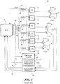
- FIG. 1 a conventional prior art gate driver system 10 employing six gate drivers 12, 14, 16, 18, 20 and 22, each driving a pair of semiconductor power switches 24, 26, 28, 30, 32, 34, respectively, such as IGBTs or MOSFETs.
- Gate drivers 12-22 are driven by high signals on lines 36, 38, and 40 and low signals on lines 42, 44, and 46, from a central controller 48, such as a microcontroller unit (MCU).
- MCU microcontroller unit
- the six high/low signals on lines 36-46 for each gate driver 12-22 are delivered through an isolation device such as an electro optic, inductive, or capacitive isolation device 50, 52, 54, 56, 58, 60, to central controller 48.
- a fault line from each gate driver 12-22 is OR-ed to fault line 62 which is also directed to central controller 48.
- Central controller 48 drives gate supply controller 64 which provides power to each of gates 12-22.
- Central controller 48 also receives signals from isolated voltage measurements 66 and current measurements 68 on lines 70, 72, 74, and 76, respectively.
- the high/low commands are typically pulse width modulated on/off commands which are conditioned and then applied by the gate drivers 12-22 to semiconductor switches 24-34.
- a typical prior art gate driver 12a uses fixed, non-programmable circuitry as shown. On/off requests occur through V in 80 and each gate driver requires an isolation circuit 82 resulting in six isolation circuits for a three phase inverter.
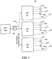
- the semiconductor power switches 24a, 26a, 28a, 30a, 32a, and 34a are driven by programmable gate controllers, in this case three programmable gate controllers 92, 94, and 96 which service the six semiconductor power switches 24a-34a in a three phase system.
- the programmable gate controllers 92, 94, 96 are remote from and communicate with central controller 48a through a single isolation device 98 over a bidirectional communication link 100, which may be implemented using a serial communication interface (SCI), a serial peripheral interface (SPI), or controller area network (CAN), for example.
- SCI serial communication interface
- SPI serial peripheral interface
- CAN controller area network
- Communication link 100 may be used to send switch control commands and parameters from central controller 48a to gate controllers 92, 94, 96 and receive feedback from gate controllers 92, 94, 96 to central controller 48a.
- Programmable gate controllers 92, 94 and 96 may be implemented with any suitable programmable device e.g. a microcontroller unit (MCU), a digital signal processor (DSP), a field programmable gate array (FPGA). These programmable gate controllers are thus capable of intelligent operation remote from the central controller 48a and proximate the semiconductor power switches.
- MCU microcontroller unit
- DSP digital signal processor
- FPGA field programmable gate array
- Measurements are made locally, such as current measurements over lines 102, 104, and 106, at the programmable gate controllers 92, 94, 96 and may be processed locally and then transmitted to the central controller 48a or applied directly to adjust operation of the semiconductor switches 24a-34a.
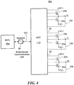
- a programmable gate controller system 90a may use a single integrated programmable gate controller 110 to service all six of the semiconductor power switches 24a-34a.
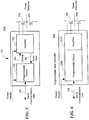
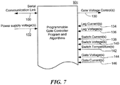
- Each programmable gate controller as exemplified by programmable gate controller 92a, Fig. 5 may include a programmable device 120 such as a DSP, an MCU, an FPGA or the like and an amplifier 122 with control 124 and feedback connections 126.
- Programmable device 120 and amplifier 122 may be realized on a single chip 123.
- Programmable gate controller, 92b, Fig. 6 may also have the programmable device 120b and the amplifier 122b integrated in one physical device.
- Programmable device 120, 120b in each case, executes the control algorithms and communicates with the central processor via the serial communication link 100. It also receives set points such as simple on/off commands or higher resolution set points such as duty cycle commands via the serial communication link 100.
- the control algorithms on a programmable device 120, 120b implement the request received via the serial link by means of control lines connected to the amplifier circuit or direct connection in the case of programmable gate controller 92b, Fig. 6 .
- control lines are pulse width modulated (PWM) signals and the amplifier 122, 122b in each case conditions the control signals so they can be applied to the gates of the power switches.
- the amplifier 122, 122b in Figs. 5 and 6 may also contain measuring circuits that can sense parameters related to the associated ones of power switches 24b, 26b such as temperature, voltage and current. These quantities are provided the programmable device 120, 120b in the form of analog signals that can be sampled and used for diagnostics, control, or protection purposes.
- the proximity of the programmable gate controller 92b and programmable device 120 (120b) close to the sensors and the power switches as well as the fact that no isolation is needed allows for implementation of very high bandwidth controls.
- Outputs include signals on serial communication link 100 and the gate voltage controls on line 130.
- Inputs include signals on communication link 100 including power supply voltage 132 as well as leg current 134, leg voltage 136, switch current 138, switch voltage 140, switch temperature 142, gate voltage(s) 144 and gate current(s) 146.
- the serial communication link 100 may employ a serial communication interface (SCI), a serial peripheral interface (SPI), or controller area network (CAN), or the like to exchange information with the central controller.
- SCI serial communication interface
- SPI serial peripheral interface
- CAN controller area network
- This information may include on/off set points for the power switches, duty-cycle and voltage/current set points, as well as timing information to synchronize the control of the switches.
- the output of the program is primarily the control signal for the actuation of the switches on line 130. At least one control line per switch is needed.
- the control line can be discrete analog or pseudo analog (PWM).
- the feedback signals 134-146 in Fig. 7 allow optimal control of the switches realizing protection algorithms and providing higher level functionality to the central controller.
- Measurements of the gate voltage and gate currents allow for the implementation of active closed loop switching controls.
- Measurements of the switch current, switch voltage and switch temperature serve as a foundation for optimization and protection algorithms.
- Measurements of leg voltages and leg currents allow for the implementation of higher level features that would otherwise be implemented by the central controller. Examples of such features are current regulation, dead time compensation, and active damping algorithms.
- Fig. 8 Software configuration is shown generally in Fig. 8 , where the gate controller program flow includes a main loop 150, communication manager 152, switch event manager 154, and switch controller 156.
- main loop 150 the routine begins with power up 158, initialization and self-checks 160, and then investigates state and fault recovery management 162 followed by processing and storage of usage data and history 164.
- Communication manager 152 after initialization and self checks establishes a link with the central processor 166. It processes incoming messages 168 and updates the switch events 170. It then prepares status and feedback information 172 and transmits them as outgoing messages 174.
- the switch event manager 154 after the initialization and self checks institutes its own initialization switch event table and switch timer 176.
- switch controller 156 initializes the gate supplies 184, monitors the switches 186 and determines whether a fault has occurred 188. If a fault has occurred there is implemented a safe shut off 190 and then if the faults have not been cleared 192 the system cycles. If the faults have been cleared it moves on to the output node 194. If no fault has occurred query is made as to whether a switch event is active 196; if it is, control switching is realized 198 and the switch model is updated 200, after which output node 194 is entered. In step 196 if the switch event is not active the system moves directly to output node 194.
- Main routine 150 is primarily responsible for configuring the controller, launching the other tasks, and implementing fault management and fault recovery algorithms at a low rate and low priority. This task can be used to process and store switch use data, such as thermal cycling information and other parameters that affect the life of the power switch.
- Communications manager 152 establishes and maintains communication with the central controller. It receives commands and synchronization information from the central controller and communicates back measurements and status information.
- Switch event manager 154 parses incoming control messages and generates switch events which are stored in the switch event table. Switch events define the timing and parameters for switch turn-on and turn-off events.
- switch controller 156 continuously monitors the state of each switch for faults such as over-current or short circuit and shoot-through conditions.
- the switch controller 156 Once the proper functioning of the switch is verified, it queries the event table for new switching events. If a new switching event has been activated, then the switch controller 156 implements the transition in an open loop or closed loop fashion based on the switching parameters provided with the switch event. Subsequent to the switching, a switch model is updated based on the measured data as indicated in step 200 of Fig. 8 . This model can be used to facilitate the controlling of the next switching event and to provide diagnostics data to the main control. If a fault is detected with a switch, then the switch controller 156 safely disables the switch and prevents any further switching until the fault condition has been cleared.
- Figs. 9 and 10 show typical turn-on and turn-off, respectively, voltage and current waveforms for a power semiconductor switch such as an IGBT in a half bridge arrangement.
- the voltage across the switch Vce drops from full blocking-voltage (typically several hundreds of volts) down to the conduction voltage (circa 2 V).
- the switch current Ic raises from 0 A to its final value. Note how the voltage does not drop significantly until the current has fully ramped-up, and the opposite diode stops conducting (the initial voltage drop is purely inductive). Only when the switch is carrying full current, does its voltage decay, first at a fast rate, and subsequently tailing off.
- the parameters of the gate control can be used to minimize turn-off losses and control the dV/dt of the turn-off and thereby mitigate EMI. Consequently, the programmable gate controller, capable of adjusting its controls in real-time, will have an advantage over a conventional gate driver with fixed settings.
- the inputs and outputs 134- 146 shown in Fig. 7 provide all information required to implement the controlled switching and switch model update.
- V ge (t) profile 210 applied to the power switches e.g. 24c via the amplifier e.g. 122c in an open loop operation.
- the profile V ge (t) 210 is constantly adjusted by software, based on actual operating conditions of the power switch 24c and information gained from the last switching event, with the object of minimizing losses and power switch component stress.
- Fig. 12 in programmable gate controller 92e the gate voltage can be controlled in a closed loop operation, with a regulator 120c implemented in software on the programmable gate controller. Note that the programmable gate controller of this invention thereby inherently offers the flexibility to implement significantly more complex switching algorithms.
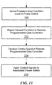
- the programmable gate controller method according to this invention is shown more generally in Fig. 13 as including sensing a predetermined condition local to the power switch 220 reporting the sensed condition to the remote programmable gate controller 222, developing one or more control signals in the remote programmable gate controller 224 and applying that control signal or signals to the associated power switch 226.
Landscapes
- Engineering & Computer Science (AREA)
- Power Engineering (AREA)
- Power Conversion In General (AREA)
- Logic Circuits (AREA)
Applications Claiming Priority (2)
| Application Number | Priority Date | Filing Date | Title |
|---|---|---|---|
| US13/385,403 US9071169B2 (en) | 2011-02-18 | 2012-02-17 | Programmable gate controller system and method |
| PCT/US2013/026325 WO2013123316A1 (en) | 2012-02-17 | 2013-02-15 | Programmable gate controller system and method |
Publications (3)
| Publication Number | Publication Date |
|---|---|
| EP2815306A1 EP2815306A1 (en) | 2014-12-24 |
| EP2815306A4 EP2815306A4 (en) | 2015-12-23 |
| EP2815306B1 true EP2815306B1 (en) | 2020-09-16 |
Family
ID=46652163
Family Applications (1)
| Application Number | Title | Priority Date | Filing Date |
|---|---|---|---|
| EP13748730.2A Active EP2815306B1 (en) | 2012-02-17 | 2013-02-15 | Programmable gate controller system and method |
Country Status (6)
| Country | Link |
|---|---|
| US (1) | US9071169B2 (enExample) |
| EP (1) | EP2815306B1 (enExample) |
| JP (1) | JP6310400B2 (enExample) |
| KR (1) | KR101986399B1 (enExample) |
| CN (1) | CN104145243A (enExample) |
| WO (1) | WO2013123316A1 (enExample) |
Families Citing this family (17)
| Publication number | Priority date | Publication date | Assignee | Title |
|---|---|---|---|---|
| GB2497967B (en) * | 2011-12-23 | 2018-02-21 | Reinhausen Maschf Scheubeck | Fault-tolerant control systems |
| CN102545711B (zh) * | 2012-02-17 | 2015-06-24 | 振发能源集团有限公司 | 一种新型的离网/并网一体化太阳能发电系统与控制方法 |
| DE102013205706A1 (de) * | 2013-03-28 | 2014-10-02 | Fraunhofer-Gesellschaft zur Förderung der angewandten Forschung e.V. | Leistungselektronische schaltung und system mit derselben |
| JP6517624B2 (ja) * | 2015-07-17 | 2019-05-22 | 三喜電機株式会社 | パワーエレクトロニクス回路用の高電圧回路のスイッチング素子開閉制御装置 |
| FR3047378B1 (fr) * | 2016-01-29 | 2018-05-18 | STMicroelectronics (Alps) SAS | Circuit de fourniture d'un signal video analogique |
| EP3460979B1 (en) * | 2016-07-01 | 2025-06-04 | Rohm Co., Ltd. | Semiconductor device |
| US10181813B2 (en) * | 2016-10-27 | 2019-01-15 | Power Integrations, Inc. | Half-bridge inverter modules with advanced protection through high-side to low-side control block communication |
| GB201620104D0 (en) * | 2016-11-28 | 2017-01-11 | Powerventure Semiconductor Ltd | A system and method of driving a switch circuit |
| JP6669125B2 (ja) * | 2017-04-27 | 2020-03-18 | 株式会社デンソー | 電力変換装置、および、これを用いた電動パワーステアリング装置 |
| CN111713019A (zh) * | 2018-02-12 | 2020-09-25 | 诺摩尔有限公司 | 一种晶体管器件 |
| CA3094062C (en) * | 2018-03-27 | 2023-09-26 | Micro Motion, Inc. | Electronics including electrical isolation |
| KR102728482B1 (ko) * | 2018-05-30 | 2024-11-08 | 서치 포 더 넥스트 리미티드 | 트랜지스터 및 다이오드를 포함하는 회로 및 소자 |
| DE102018218821A1 (de) * | 2018-11-05 | 2020-05-07 | Volkswagen Aktiengesellschaft | Vorrichtung und Verfahren zum Ansteuern von Schaltelementen eines Stromrichters |
| US10979041B1 (en) * | 2020-03-13 | 2021-04-13 | Hamilton Sunstrand Corporation | Method for monitoring gate drive signals for power module aging effects |
| US11342855B2 (en) * | 2020-04-17 | 2022-05-24 | Infineon Technologies Austria Ag | Controlling a switch across an isolation barrier |
| JP7325632B2 (ja) * | 2020-06-01 | 2023-08-14 | 三菱電機株式会社 | パワー半導体素子の駆動制御装置、及び、パワーモジュール |
| EP4564678A1 (en) * | 2023-12-01 | 2025-06-04 | Infineon Technologies Austria AG | Programmable gate driver circuit for an integrated power switch |
Citations (1)
| Publication number | Priority date | Publication date | Assignee | Title |
|---|---|---|---|---|
| US20090168469A1 (en) * | 2007-12-28 | 2009-07-02 | International Business Machines Corporation | Apparatus, system, and method for a low cost fault-tolerant power supply |
Family Cites Families (16)
| Publication number | Priority date | Publication date | Assignee | Title |
|---|---|---|---|---|
| US4425628A (en) | 1981-05-26 | 1984-01-10 | General Electric Company | Control module for engergy management system |
| US4528662A (en) | 1983-10-07 | 1985-07-09 | United Technologies Automotive, Inc. | Multiplex control system having enhanced integrity |
| DE4403941C2 (de) * | 1994-02-08 | 2000-05-18 | Abb Schweiz Ag | Verfahren und Schaltungsanordnung zur Ansteuerung von Halbleiterschaltern einer Reihenschaltung |
| AUPN422295A0 (en) | 1995-07-18 | 1995-08-10 | Bytecraft Research Pty. Ltd. | Control system |
| JP3546578B2 (ja) * | 1996-02-28 | 2004-07-28 | 三菱電機株式会社 | 電流検出装置 |
| US6005377A (en) * | 1997-09-17 | 1999-12-21 | Lucent Technologies Inc. | Programmable digital controller for switch mode power conversion and power supply employing the same |
| JP4044861B2 (ja) * | 2003-04-03 | 2008-02-06 | 三菱電機株式会社 | 電力変換装置およびその電力変換装置を備える電力変換システム装置 |
| CN100466473C (zh) * | 2003-09-03 | 2009-03-04 | Nxp股份有限公司 | 并联mosfet的失效预测 |
| US7026798B2 (en) * | 2003-10-27 | 2006-04-11 | Intersil Americas Inc. | Multi-channel driver interface circuit for increasing phase count in a multi-phase DC-DC converter |
| JP4223379B2 (ja) * | 2003-12-10 | 2009-02-12 | 三菱電機株式会社 | スイッチングデバイスの制御装置およびモーターの駆動回路の制御装置 |
| JP4212546B2 (ja) * | 2004-11-15 | 2009-01-21 | 株式会社東芝 | 電力変換装置 |
| US7839201B2 (en) * | 2005-04-01 | 2010-11-23 | Raytheon Company | Integrated smart power switch |
| ES2353520T3 (es) * | 2005-08-01 | 2011-03-02 | Agie Charmilles Sa | Procedimiento de funcionamiento de una máquina de mecanizado por electroerosión y un sistema de mecanizado por electroerosión. |
| KR100964631B1 (ko) * | 2008-04-29 | 2010-06-22 | 한국철도기술연구원 | 가선전압 안정화 기능을 구비한 직류 전동차용 급전 시스템 |
| JP2010263712A (ja) * | 2009-05-08 | 2010-11-18 | Mitsuba Corp | モータ駆動装置、及び、モータ駆動システム |
| US20110161420A1 (en) | 2009-12-30 | 2011-06-30 | Dealto Rachel Kathryn | Computer-implemented system and method for creating opportunities to connect people together |
-
2012
- 2012-02-17 US US13/385,403 patent/US9071169B2/en active Active
-
2013
- 2013-02-15 WO PCT/US2013/026325 patent/WO2013123316A1/en not_active Ceased
- 2013-02-15 EP EP13748730.2A patent/EP2815306B1/en active Active
- 2013-02-15 JP JP2014557812A patent/JP6310400B2/ja active Active
- 2013-02-15 CN CN201380009831.9A patent/CN104145243A/zh active Pending
- 2013-02-15 KR KR1020147024754A patent/KR101986399B1/ko active Active
Patent Citations (1)
| Publication number | Priority date | Publication date | Assignee | Title |
|---|---|---|---|---|
| US20090168469A1 (en) * | 2007-12-28 | 2009-07-02 | International Business Machines Corporation | Apparatus, system, and method for a low cost fault-tolerant power supply |
Also Published As
| Publication number | Publication date |
|---|---|
| EP2815306A1 (en) | 2014-12-24 |
| WO2013123316A1 (en) | 2013-08-22 |
| US9071169B2 (en) | 2015-06-30 |
| KR20140129089A (ko) | 2014-11-06 |
| JP2015515242A (ja) | 2015-05-21 |
| JP6310400B2 (ja) | 2018-04-11 |
| EP2815306A4 (en) | 2015-12-23 |
| KR101986399B1 (ko) | 2019-06-05 |
| CN104145243A (zh) | 2014-11-12 |
| US20120212075A1 (en) | 2012-08-23 |
Similar Documents
| Publication | Publication Date | Title |
|---|---|---|
| EP2815306B1 (en) | Programmable gate controller system and method | |
| US11283438B2 (en) | Gate drive apparatus | |
| JP6438018B2 (ja) | 並列電力スイッチの同期 | |
| US7868597B2 (en) | Dead-time transition adjustments for synchronous power converters | |
| CN106487225B (zh) | 开关电源装置 | |
| JP6196984B2 (ja) | 半導体装置制御器 | |
| US8860398B2 (en) | Edge rate control gate driver for switching power converters | |
| US10250150B2 (en) | Method for driving a resonant converter, and corresponding converter and computer program product | |
| EP4102720A1 (en) | Actively tracking switching speed control and regulating switching speed of a power transistor during turn-on | |
| KR20100130161A (ko) | 다상 부스트 컨버터와 그 작동방법 | |
| CN103151920A (zh) | 自适应死时间控制 | |
| CN101277066A (zh) | 多路稳压隔离式数字dc/dc电源及控制方法 | |
| CN104467445A (zh) | 具有动态相位触发的多相降压转换器 | |
| CA2769814C (en) | Programmable gate controller system and method | |
| US20190044456A1 (en) | Three-level inverter switching | |
| US6411534B1 (en) | Control methods for power converter circuit | |
| US20230023250A1 (en) | Switching circuit | |
| Lüdecke | Compensating asymmetries of parallel-connected SiC MOSFETs using intelligent gate drivers | |
| CN115224670A (zh) | 用于功率转换器的安全切断电路 | |
| CN206274644U (zh) | 结合电感转换器使用的振荡器以及电感转换器 | |
| Tian et al. | A passive component based gate drive scheme for negative gate voltage spike mitigation in a sic-based dual-active bridge | |
| WO2020109777A1 (en) | Gate driver | |
| US10520967B2 (en) | Power converter with a boost unit including at least two boost chopper circuits connected in parallel | |
| Liu et al. | Design of an Active Gate Driver IC for E-Mode GaN HEMTs Based on Adaptive Phased Regulation | |
| WO2018053205A1 (en) | Multiphase power controller with dynamic phase management |
Legal Events
| Date | Code | Title | Description |
|---|---|---|---|
| PUAI | Public reference made under article 153(3) epc to a published international application that has entered the european phase |
Free format text: ORIGINAL CODE: 0009012 |
|
| 17P | Request for examination filed |
Effective date: 20140814 |
|
| AK | Designated contracting states |
Kind code of ref document: A1 Designated state(s): AL AT BE BG CH CY CZ DE DK EE ES FI FR GB GR HR HU IE IS IT LI LT LU LV MC MK MT NL NO PL PT RO RS SE SI SK SM TR |
|
| AX | Request for extension of the european patent |
Extension state: BA ME |
|
| RAP1 | Party data changed (applicant data changed or rights of an application transferred) |
Owner name: GE HYBRID TECHNOLOGIES, LLC |
|
| DAX | Request for extension of the european patent (deleted) | ||
| RA4 | Supplementary search report drawn up and despatched (corrected) |
Effective date: 20151123 |
|
| RIC1 | Information provided on ipc code assigned before grant |
Ipc: H02M 1/08 20060101ALI20151117BHEP Ipc: H03K 17/18 20060101ALI20151117BHEP Ipc: G06F 9/00 20060101AFI20151117BHEP Ipc: H03K 17/082 20060101ALI20151117BHEP |
|
| STAA | Information on the status of an ep patent application or granted ep patent |
Free format text: STATUS: EXAMINATION IS IN PROGRESS |
|
| 17Q | First examination report despatched |
Effective date: 20180806 |
|
| GRAP | Despatch of communication of intention to grant a patent |
Free format text: ORIGINAL CODE: EPIDOSNIGR1 |
|
| STAA | Information on the status of an ep patent application or granted ep patent |
Free format text: STATUS: GRANT OF PATENT IS INTENDED |
|
| INTG | Intention to grant announced |
Effective date: 20200428 |
|
| GRAS | Grant fee paid |
Free format text: ORIGINAL CODE: EPIDOSNIGR3 |
|
| GRAA | (expected) grant |
Free format text: ORIGINAL CODE: 0009210 |
|
| STAA | Information on the status of an ep patent application or granted ep patent |
Free format text: STATUS: THE PATENT HAS BEEN GRANTED |
|
| AK | Designated contracting states |
Kind code of ref document: B1 Designated state(s): AL AT BE BG CH CY CZ DE DK EE ES FI FR GB GR HR HU IE IS IT LI LT LU LV MC MK MT NL NO PL PT RO RS SE SI SK SM TR |
|
| RAP1 | Party data changed (applicant data changed or rights of an application transferred) |
Owner name: GE HYBRID TECHNOLOGIES, LLC |
|
| REG | Reference to a national code |
Ref country code: GB Ref legal event code: FG4D |
|
| REG | Reference to a national code |
Ref country code: CH Ref legal event code: EP |
|
| REG | Reference to a national code |
Ref country code: DE Ref legal event code: R096 Ref document number: 602013072582 Country of ref document: DE |
|
| REG | Reference to a national code |
Ref country code: IE Ref legal event code: FG4D |
|
| REG | Reference to a national code |
Ref country code: AT Ref legal event code: REF Ref document number: 1314746 Country of ref document: AT Kind code of ref document: T Effective date: 20201015 |
|
| PG25 | Lapsed in a contracting state [announced via postgrant information from national office to epo] |
Ref country code: HR Free format text: LAPSE BECAUSE OF FAILURE TO SUBMIT A TRANSLATION OF THE DESCRIPTION OR TO PAY THE FEE WITHIN THE PRESCRIBED TIME-LIMIT Effective date: 20200916 Ref country code: FI Free format text: LAPSE BECAUSE OF FAILURE TO SUBMIT A TRANSLATION OF THE DESCRIPTION OR TO PAY THE FEE WITHIN THE PRESCRIBED TIME-LIMIT Effective date: 20200916 Ref country code: NO Free format text: LAPSE BECAUSE OF FAILURE TO SUBMIT A TRANSLATION OF THE DESCRIPTION OR TO PAY THE FEE WITHIN THE PRESCRIBED TIME-LIMIT Effective date: 20201216 Ref country code: SE Free format text: LAPSE BECAUSE OF FAILURE TO SUBMIT A TRANSLATION OF THE DESCRIPTION OR TO PAY THE FEE WITHIN THE PRESCRIBED TIME-LIMIT Effective date: 20200916 Ref country code: BG Free format text: LAPSE BECAUSE OF FAILURE TO SUBMIT A TRANSLATION OF THE DESCRIPTION OR TO PAY THE FEE WITHIN THE PRESCRIBED TIME-LIMIT Effective date: 20201216 Ref country code: GR Free format text: LAPSE BECAUSE OF FAILURE TO SUBMIT A TRANSLATION OF THE DESCRIPTION OR TO PAY THE FEE WITHIN THE PRESCRIBED TIME-LIMIT Effective date: 20201217 |
|
| REG | Reference to a national code |
Ref country code: AT Ref legal event code: MK05 Ref document number: 1314746 Country of ref document: AT Kind code of ref document: T Effective date: 20200916 |
|
| REG | Reference to a national code |
Ref country code: NL Ref legal event code: MP Effective date: 20200916 |
|
| PG25 | Lapsed in a contracting state [announced via postgrant information from national office to epo] |
Ref country code: LV Free format text: LAPSE BECAUSE OF FAILURE TO SUBMIT A TRANSLATION OF THE DESCRIPTION OR TO PAY THE FEE WITHIN THE PRESCRIBED TIME-LIMIT Effective date: 20200916 Ref country code: RS Free format text: LAPSE BECAUSE OF FAILURE TO SUBMIT A TRANSLATION OF THE DESCRIPTION OR TO PAY THE FEE WITHIN THE PRESCRIBED TIME-LIMIT Effective date: 20200916 |
|
| REG | Reference to a national code |
Ref country code: LT Ref legal event code: MG4D |
|
| PG25 | Lapsed in a contracting state [announced via postgrant information from national office to epo] |
Ref country code: SM Free format text: LAPSE BECAUSE OF FAILURE TO SUBMIT A TRANSLATION OF THE DESCRIPTION OR TO PAY THE FEE WITHIN THE PRESCRIBED TIME-LIMIT Effective date: 20200916 Ref country code: RO Free format text: LAPSE BECAUSE OF FAILURE TO SUBMIT A TRANSLATION OF THE DESCRIPTION OR TO PAY THE FEE WITHIN THE PRESCRIBED TIME-LIMIT Effective date: 20200916 Ref country code: NL Free format text: LAPSE BECAUSE OF FAILURE TO SUBMIT A TRANSLATION OF THE DESCRIPTION OR TO PAY THE FEE WITHIN THE PRESCRIBED TIME-LIMIT Effective date: 20200916 Ref country code: PT Free format text: LAPSE BECAUSE OF FAILURE TO SUBMIT A TRANSLATION OF THE DESCRIPTION OR TO PAY THE FEE WITHIN THE PRESCRIBED TIME-LIMIT Effective date: 20210118 Ref country code: LT Free format text: LAPSE BECAUSE OF FAILURE TO SUBMIT A TRANSLATION OF THE DESCRIPTION OR TO PAY THE FEE WITHIN THE PRESCRIBED TIME-LIMIT Effective date: 20200916 Ref country code: CZ Free format text: LAPSE BECAUSE OF FAILURE TO SUBMIT A TRANSLATION OF THE DESCRIPTION OR TO PAY THE FEE WITHIN THE PRESCRIBED TIME-LIMIT Effective date: 20200916 Ref country code: EE Free format text: LAPSE BECAUSE OF FAILURE TO SUBMIT A TRANSLATION OF THE DESCRIPTION OR TO PAY THE FEE WITHIN THE PRESCRIBED TIME-LIMIT Effective date: 20200916 |
|
| PG25 | Lapsed in a contracting state [announced via postgrant information from national office to epo] |
Ref country code: ES Free format text: LAPSE BECAUSE OF FAILURE TO SUBMIT A TRANSLATION OF THE DESCRIPTION OR TO PAY THE FEE WITHIN THE PRESCRIBED TIME-LIMIT Effective date: 20200916 Ref country code: AL Free format text: LAPSE BECAUSE OF FAILURE TO SUBMIT A TRANSLATION OF THE DESCRIPTION OR TO PAY THE FEE WITHIN THE PRESCRIBED TIME-LIMIT Effective date: 20200916 Ref country code: AT Free format text: LAPSE BECAUSE OF FAILURE TO SUBMIT A TRANSLATION OF THE DESCRIPTION OR TO PAY THE FEE WITHIN THE PRESCRIBED TIME-LIMIT Effective date: 20200916 Ref country code: IS Free format text: LAPSE BECAUSE OF FAILURE TO SUBMIT A TRANSLATION OF THE DESCRIPTION OR TO PAY THE FEE WITHIN THE PRESCRIBED TIME-LIMIT Effective date: 20210116 Ref country code: PL Free format text: LAPSE BECAUSE OF FAILURE TO SUBMIT A TRANSLATION OF THE DESCRIPTION OR TO PAY THE FEE WITHIN THE PRESCRIBED TIME-LIMIT Effective date: 20200916 |
|
| REG | Reference to a national code |
Ref country code: DE Ref legal event code: R097 Ref document number: 602013072582 Country of ref document: DE |
|
| PG25 | Lapsed in a contracting state [announced via postgrant information from national office to epo] |
Ref country code: SK Free format text: LAPSE BECAUSE OF FAILURE TO SUBMIT A TRANSLATION OF THE DESCRIPTION OR TO PAY THE FEE WITHIN THE PRESCRIBED TIME-LIMIT Effective date: 20200916 |
|
| PLBE | No opposition filed within time limit |
Free format text: ORIGINAL CODE: 0009261 |
|
| STAA | Information on the status of an ep patent application or granted ep patent |
Free format text: STATUS: NO OPPOSITION FILED WITHIN TIME LIMIT |
|
| 26N | No opposition filed |
Effective date: 20210617 |
|
| PG25 | Lapsed in a contracting state [announced via postgrant information from national office to epo] |
Ref country code: SI Free format text: LAPSE BECAUSE OF FAILURE TO SUBMIT A TRANSLATION OF THE DESCRIPTION OR TO PAY THE FEE WITHIN THE PRESCRIBED TIME-LIMIT Effective date: 20200916 Ref country code: DK Free format text: LAPSE BECAUSE OF FAILURE TO SUBMIT A TRANSLATION OF THE DESCRIPTION OR TO PAY THE FEE WITHIN THE PRESCRIBED TIME-LIMIT Effective date: 20200916 |
|
| PG25 | Lapsed in a contracting state [announced via postgrant information from national office to epo] |
Ref country code: MC Free format text: LAPSE BECAUSE OF FAILURE TO SUBMIT A TRANSLATION OF THE DESCRIPTION OR TO PAY THE FEE WITHIN THE PRESCRIBED TIME-LIMIT Effective date: 20200916 |
|
| GBPC | Gb: european patent ceased through non-payment of renewal fee |
Effective date: 20210215 |
|
| REG | Reference to a national code |
Ref country code: BE Ref legal event code: MM Effective date: 20210228 |
|
| PG25 | Lapsed in a contracting state [announced via postgrant information from national office to epo] |
Ref country code: LU Free format text: LAPSE BECAUSE OF NON-PAYMENT OF DUE FEES Effective date: 20210215 Ref country code: LI Free format text: LAPSE BECAUSE OF NON-PAYMENT OF DUE FEES Effective date: 20210228 Ref country code: IT Free format text: LAPSE BECAUSE OF FAILURE TO SUBMIT A TRANSLATION OF THE DESCRIPTION OR TO PAY THE FEE WITHIN THE PRESCRIBED TIME-LIMIT Effective date: 20200916 Ref country code: CH Free format text: LAPSE BECAUSE OF NON-PAYMENT OF DUE FEES Effective date: 20210228 |
|
| PG25 | Lapsed in a contracting state [announced via postgrant information from national office to epo] |
Ref country code: IE Free format text: LAPSE BECAUSE OF NON-PAYMENT OF DUE FEES Effective date: 20210215 Ref country code: GB Free format text: LAPSE BECAUSE OF NON-PAYMENT OF DUE FEES Effective date: 20210215 Ref country code: FR Free format text: LAPSE BECAUSE OF NON-PAYMENT OF DUE FEES Effective date: 20210228 |
|
| PG25 | Lapsed in a contracting state [announced via postgrant information from national office to epo] |
Ref country code: BE Free format text: LAPSE BECAUSE OF NON-PAYMENT OF DUE FEES Effective date: 20210228 |
|
| PG25 | Lapsed in a contracting state [announced via postgrant information from national office to epo] |
Ref country code: HU Free format text: LAPSE BECAUSE OF FAILURE TO SUBMIT A TRANSLATION OF THE DESCRIPTION OR TO PAY THE FEE WITHIN THE PRESCRIBED TIME-LIMIT; INVALID AB INITIO Effective date: 20130215 |
|
| PG25 | Lapsed in a contracting state [announced via postgrant information from national office to epo] |
Ref country code: CY Free format text: LAPSE BECAUSE OF FAILURE TO SUBMIT A TRANSLATION OF THE DESCRIPTION OR TO PAY THE FEE WITHIN THE PRESCRIBED TIME-LIMIT Effective date: 20200916 |
|
| P01 | Opt-out of the competence of the unified patent court (upc) registered |
Effective date: 20230528 |
|
| PG25 | Lapsed in a contracting state [announced via postgrant information from national office to epo] |
Ref country code: MK Free format text: LAPSE BECAUSE OF FAILURE TO SUBMIT A TRANSLATION OF THE DESCRIPTION OR TO PAY THE FEE WITHIN THE PRESCRIBED TIME-LIMIT Effective date: 20200916 |
|
| PG25 | Lapsed in a contracting state [announced via postgrant information from national office to epo] |
Ref country code: TR Free format text: LAPSE BECAUSE OF FAILURE TO SUBMIT A TRANSLATION OF THE DESCRIPTION OR TO PAY THE FEE WITHIN THE PRESCRIBED TIME-LIMIT Effective date: 20200916 |
|
| PG25 | Lapsed in a contracting state [announced via postgrant information from national office to epo] |
Ref country code: MT Free format text: LAPSE BECAUSE OF FAILURE TO SUBMIT A TRANSLATION OF THE DESCRIPTION OR TO PAY THE FEE WITHIN THE PRESCRIBED TIME-LIMIT Effective date: 20200916 |
|
| PGFP | Annual fee paid to national office [announced via postgrant information from national office to epo] |
Ref country code: DE Payment date: 20250122 Year of fee payment: 13 |