EP2812708B1 - Procédé d'analyse d'un analyte avec des nano-entonnoirs fluidiques - Google Patents
Procédé d'analyse d'un analyte avec des nano-entonnoirs fluidiques Download PDFInfo
- Publication number
- EP2812708B1 EP2812708B1 EP13746055.6A EP13746055A EP2812708B1 EP 2812708 B1 EP2812708 B1 EP 2812708B1 EP 13746055 A EP13746055 A EP 13746055A EP 2812708 B1 EP2812708 B1 EP 2812708B1
- Authority
- EP
- European Patent Office
- Prior art keywords
- nanofunnel
- nanochannel
- depth
- width
- funnel
- Prior art date
- Legal status (The legal status is an assumption and is not a legal conclusion. Google has not performed a legal analysis and makes no representation as to the accuracy of the status listed.)
- Active
Links
- 238000000034 method Methods 0.000 title claims description 36
- 239000012491 analyte Substances 0.000 title claims description 24
- 239000002090 nanochannel Substances 0.000 claims description 170
- 239000012530 fluid Substances 0.000 claims description 8
- 238000013507 mapping Methods 0.000 claims description 7
- 238000007306 functionalization reaction Methods 0.000 claims description 2
- 108091028043 Nucleic acid sequence Proteins 0.000 claims 1
- 108020004414 DNA Proteins 0.000 description 94
- 238000003801 milling Methods 0.000 description 71
- 239000000758 substrate Substances 0.000 description 39
- 102000053602 DNA Human genes 0.000 description 32
- 230000006870 function Effects 0.000 description 26
- 230000005684 electric field Effects 0.000 description 20
- 238000000059 patterning Methods 0.000 description 20
- 238000010884 ion-beam technique Methods 0.000 description 18
- 230000005945 translocation Effects 0.000 description 16
- 230000000875 corresponding effect Effects 0.000 description 15
- 238000004458 analytical method Methods 0.000 description 12
- 239000000463 material Substances 0.000 description 12
- 239000000523 sample Substances 0.000 description 11
- 230000004888 barrier function Effects 0.000 description 10
- 239000010410 layer Substances 0.000 description 10
- 238000004519 manufacturing process Methods 0.000 description 8
- VYPSYNLAJGMNEJ-UHFFFAOYSA-N silicon dioxide Inorganic materials O=[Si]=O VYPSYNLAJGMNEJ-UHFFFAOYSA-N 0.000 description 8
- 241000701959 Escherichia virus Lambda Species 0.000 description 7
- 229920002521 macromolecule Polymers 0.000 description 7
- 239000002245 particle Substances 0.000 description 7
- 238000004891 communication Methods 0.000 description 6
- 238000011960 computer-aided design Methods 0.000 description 6
- 230000001419 dependent effect Effects 0.000 description 6
- 238000002474 experimental method Methods 0.000 description 6
- 230000008569 process Effects 0.000 description 6
- 239000010453 quartz Substances 0.000 description 6
- 238000004630 atomic force microscopy Methods 0.000 description 5
- 230000008901 benefit Effects 0.000 description 5
- 230000008859 change Effects 0.000 description 5
- 230000000694 effects Effects 0.000 description 5
- 229910052751 metal Inorganic materials 0.000 description 5
- 239000002184 metal Substances 0.000 description 5
- 229920000642 polymer Polymers 0.000 description 5
- 229920000036 polyvinylpyrrolidone Polymers 0.000 description 5
- 235000013855 polyvinylpyrrolidone Nutrition 0.000 description 5
- 239000001267 polyvinylpyrrolidone Substances 0.000 description 5
- 238000001878 scanning electron micrograph Methods 0.000 description 5
- 238000012163 sequencing technique Methods 0.000 description 5
- 238000004088 simulation Methods 0.000 description 5
- 230000007423 decrease Effects 0.000 description 4
- 238000005516 engineering process Methods 0.000 description 4
- 238000005530 etching Methods 0.000 description 4
- 238000002073 fluorescence micrograph Methods 0.000 description 4
- 150000002500 ions Chemical class 0.000 description 4
- 238000005259 measurement Methods 0.000 description 4
- 238000004513 sizing Methods 0.000 description 4
- 238000000089 atomic force micrograph Methods 0.000 description 3
- 229920001222 biopolymer Polymers 0.000 description 3
- 230000000873 masking effect Effects 0.000 description 3
- 239000000178 monomer Substances 0.000 description 3
- 230000003287 optical effect Effects 0.000 description 3
- 102000040430 polynucleotide Human genes 0.000 description 3
- 108091033319 polynucleotide Proteins 0.000 description 3
- 239000002157 polynucleotide Substances 0.000 description 3
- 229910052710 silicon Inorganic materials 0.000 description 3
- 239000007779 soft material Substances 0.000 description 3
- 238000004166 bioassay Methods 0.000 description 2
- 230000000295 complement effect Effects 0.000 description 2
- 230000002596 correlated effect Effects 0.000 description 2
- 239000004205 dimethyl polysiloxane Substances 0.000 description 2
- 238000001962 electrophoresis Methods 0.000 description 2
- 238000004049 embossing Methods 0.000 description 2
- 238000011156 evaluation Methods 0.000 description 2
- -1 features Substances 0.000 description 2
- 238000000799 fluorescence microscopy Methods 0.000 description 2
- 239000011521 glass Substances 0.000 description 2
- 238000011835 investigation Methods 0.000 description 2
- 230000000670 limiting effect Effects 0.000 description 2
- 150000002739 metals Chemical class 0.000 description 2
- 238000004377 microelectronic Methods 0.000 description 2
- 238000012986 modification Methods 0.000 description 2
- 230000004048 modification Effects 0.000 description 2
- 238000000465 moulding Methods 0.000 description 2
- 102000039446 nucleic acids Human genes 0.000 description 2
- 108020004707 nucleic acids Proteins 0.000 description 2
- 150000007523 nucleic acids Chemical class 0.000 description 2
- 230000000704 physical effect Effects 0.000 description 2
- 238000000053 physical method Methods 0.000 description 2
- 229920003023 plastic Polymers 0.000 description 2
- 239000004033 plastic Substances 0.000 description 2
- 229920000435 poly(dimethylsiloxane) Polymers 0.000 description 2
- 229920003229 poly(methyl methacrylate) Polymers 0.000 description 2
- 239000004926 polymethyl methacrylate Substances 0.000 description 2
- 239000002243 precursor Substances 0.000 description 2
- 102000004169 proteins and genes Human genes 0.000 description 2
- 108090000623 proteins and genes Proteins 0.000 description 2
- 239000010703 silicon Substances 0.000 description 2
- 238000004557 single molecule detection Methods 0.000 description 2
- 239000007787 solid Substances 0.000 description 2
- 239000000243 solution Substances 0.000 description 2
- 230000005641 tunneling Effects 0.000 description 2
- 229910052581 Si3N4 Inorganic materials 0.000 description 1
- GRRMZXFOOGQMFA-UHFFFAOYSA-J YoYo-1 Chemical compound [I-].[I-].[I-].[I-].C12=CC=CC=C2C(C=C2N(C3=CC=CC=C3O2)C)=CC=[N+]1CCC[N+](C)(C)CCC[N+](C)(C)CCC[N+](C1=CC=CC=C11)=CC=C1C=C1N(C)C2=CC=CC=C2O1 GRRMZXFOOGQMFA-UHFFFAOYSA-J 0.000 description 1
- 238000004026 adhesive bonding Methods 0.000 description 1
- WYTGDNHDOZPMIW-RCBQFDQVSA-N alstonine Natural products C1=CC2=C3C=CC=CC3=NC2=C2N1C[C@H]1[C@H](C)OC=C(C(=O)OC)[C@H]1C2 WYTGDNHDOZPMIW-RCBQFDQVSA-N 0.000 description 1
- 238000013459 approach Methods 0.000 description 1
- 238000003491 array Methods 0.000 description 1
- 230000015572 biosynthetic process Effects 0.000 description 1
- 238000004364 calculation method Methods 0.000 description 1
- 230000006037 cell lysis Effects 0.000 description 1
- 239000000919 ceramic Substances 0.000 description 1
- 238000012512 characterization method Methods 0.000 description 1
- 229910052804 chromium Inorganic materials 0.000 description 1
- 229910052681 coesite Inorganic materials 0.000 description 1
- 230000006835 compression Effects 0.000 description 1
- 238000007906 compression Methods 0.000 description 1
- 238000010276 construction Methods 0.000 description 1
- 229910052906 cristobalite Inorganic materials 0.000 description 1
- 230000003247 decreasing effect Effects 0.000 description 1
- 230000008021 deposition Effects 0.000 description 1
- 238000005137 deposition process Methods 0.000 description 1
- 238000013461 design Methods 0.000 description 1
- 239000010432 diamond Substances 0.000 description 1
- 239000000975 dye Substances 0.000 description 1
- 229920001971 elastomer Polymers 0.000 description 1
- 239000000806 elastomer Substances 0.000 description 1
- 238000010894 electron beam technology Methods 0.000 description 1
- 238000005370 electroosmosis Methods 0.000 description 1
- 230000001973 epigenetic effect Effects 0.000 description 1
- 230000005284 excitation Effects 0.000 description 1
- 230000002349 favourable effect Effects 0.000 description 1
- 238000004401 flow injection analysis Methods 0.000 description 1
- 239000007850 fluorescent dye Substances 0.000 description 1
- 230000004927 fusion Effects 0.000 description 1
- 238000010191 image analysis Methods 0.000 description 1
- 238000003384 imaging method Methods 0.000 description 1
- 238000007654 immersion Methods 0.000 description 1
- 238000010348 incorporation Methods 0.000 description 1
- 230000000977 initiatory effect Effects 0.000 description 1
- 239000012212 insulator Substances 0.000 description 1
- 230000010354 integration Effects 0.000 description 1
- 238000009830 intercalation Methods 0.000 description 1
- 230000009878 intermolecular interaction Effects 0.000 description 1
- 238000002955 isolation Methods 0.000 description 1
- 238000002032 lab-on-a-chip Methods 0.000 description 1
- 238000013178 mathematical model Methods 0.000 description 1
- 239000011159 matrix material Substances 0.000 description 1
- 239000012528 membrane Substances 0.000 description 1
- QSHDDOUJBYECFT-UHFFFAOYSA-N mercury Chemical compound [Hg] QSHDDOUJBYECFT-UHFFFAOYSA-N 0.000 description 1
- 229910052753 mercury Inorganic materials 0.000 description 1
- 238000000329 molecular dynamics simulation Methods 0.000 description 1
- 239000002086 nanomaterial Substances 0.000 description 1
- 239000002773 nucleotide Substances 0.000 description 1
- 125000003729 nucleotide group Chemical group 0.000 description 1
- 229910052697 platinum Inorganic materials 0.000 description 1
- 229920000867 polyelectrolyte Polymers 0.000 description 1
- 229920002635 polyurethane Polymers 0.000 description 1
- 239000004814 polyurethane Substances 0.000 description 1
- 238000002360 preparation method Methods 0.000 description 1
- 238000012545 processing Methods 0.000 description 1
- 230000009467 reduction Effects 0.000 description 1
- 230000002829 reductive effect Effects 0.000 description 1
- 238000011160 research Methods 0.000 description 1
- 230000004044 response Effects 0.000 description 1
- 230000002441 reversible effect Effects 0.000 description 1
- 238000007789 sealing Methods 0.000 description 1
- 239000004065 semiconductor Substances 0.000 description 1
- 230000035945 sensitivity Effects 0.000 description 1
- 238000000926 separation method Methods 0.000 description 1
- 239000000377 silicon dioxide Substances 0.000 description 1
- HQVNEWCFYHHQES-UHFFFAOYSA-N silicon nitride Chemical compound N12[Si]34N5[Si]62N3[Si]51N64 HQVNEWCFYHHQES-UHFFFAOYSA-N 0.000 description 1
- 239000002356 single layer Substances 0.000 description 1
- 239000007790 solid phase Substances 0.000 description 1
- 239000002904 solvent Substances 0.000 description 1
- 229910052682 stishovite Inorganic materials 0.000 description 1
- 239000000126 substance Substances 0.000 description 1
- 238000003325 tomography Methods 0.000 description 1
- 230000007704 transition Effects 0.000 description 1
- 229910052905 tridymite Inorganic materials 0.000 description 1
Images


Classifications
-
- G—PHYSICS
- G01—MEASURING; TESTING
- G01N—INVESTIGATING OR ANALYSING MATERIALS BY DETERMINING THEIR CHEMICAL OR PHYSICAL PROPERTIES
- G01N33/00—Investigating or analysing materials by specific methods not covered by groups G01N1/00 - G01N31/00
- G01N33/48—Biological material, e.g. blood, urine; Haemocytometers
- G01N33/483—Physical analysis of biological material
- G01N33/487—Physical analysis of biological material of liquid biological material
- G01N33/48707—Physical analysis of biological material of liquid biological material by electrical means
- G01N33/48721—Investigating individual macromolecules, e.g. by translocation through nanopores
-
- B—PERFORMING OPERATIONS; TRANSPORTING
- B01—PHYSICAL OR CHEMICAL PROCESSES OR APPARATUS IN GENERAL
- B01L—CHEMICAL OR PHYSICAL LABORATORY APPARATUS FOR GENERAL USE
- B01L3/00—Containers or dishes for laboratory use, e.g. laboratory glassware; Droppers
- B01L3/50—Containers for the purpose of retaining a material to be analysed, e.g. test tubes
- B01L3/502—Containers for the purpose of retaining a material to be analysed, e.g. test tubes with fluid transport, e.g. in multi-compartment structures
- B01L3/5027—Containers for the purpose of retaining a material to be analysed, e.g. test tubes with fluid transport, e.g. in multi-compartment structures by integrated microfluidic structures, i.e. dimensions of channels and chambers are such that surface tension forces are important, e.g. lab-on-a-chip
- B01L3/502707—Containers for the purpose of retaining a material to be analysed, e.g. test tubes with fluid transport, e.g. in multi-compartment structures by integrated microfluidic structures, i.e. dimensions of channels and chambers are such that surface tension forces are important, e.g. lab-on-a-chip characterised by the manufacture of the container or its components
-
- B—PERFORMING OPERATIONS; TRANSPORTING
- B01—PHYSICAL OR CHEMICAL PROCESSES OR APPARATUS IN GENERAL
- B01L—CHEMICAL OR PHYSICAL LABORATORY APPARATUS FOR GENERAL USE
- B01L3/00—Containers or dishes for laboratory use, e.g. laboratory glassware; Droppers
- B01L3/50—Containers for the purpose of retaining a material to be analysed, e.g. test tubes
- B01L3/502—Containers for the purpose of retaining a material to be analysed, e.g. test tubes with fluid transport, e.g. in multi-compartment structures
- B01L3/5027—Containers for the purpose of retaining a material to be analysed, e.g. test tubes with fluid transport, e.g. in multi-compartment structures by integrated microfluidic structures, i.e. dimensions of channels and chambers are such that surface tension forces are important, e.g. lab-on-a-chip
- B01L3/502761—Containers for the purpose of retaining a material to be analysed, e.g. test tubes with fluid transport, e.g. in multi-compartment structures by integrated microfluidic structures, i.e. dimensions of channels and chambers are such that surface tension forces are important, e.g. lab-on-a-chip specially adapted for handling suspended solids or molecules independently from the bulk fluid flow, e.g. for trapping or sorting beads, for physically stretching molecules
-
- B—PERFORMING OPERATIONS; TRANSPORTING
- B29—WORKING OF PLASTICS; WORKING OF SUBSTANCES IN A PLASTIC STATE IN GENERAL
- B29C—SHAPING OR JOINING OF PLASTICS; SHAPING OF MATERIAL IN A PLASTIC STATE, NOT OTHERWISE PROVIDED FOR; AFTER-TREATMENT OF THE SHAPED PRODUCTS, e.g. REPAIRING
- B29C59/00—Surface shaping of articles, e.g. embossing; Apparatus therefor
- B29C59/16—Surface shaping of articles, e.g. embossing; Apparatus therefor by wave energy or particle radiation, e.g. infrared heating
-
- C—CHEMISTRY; METALLURGY
- C12—BIOCHEMISTRY; BEER; SPIRITS; WINE; VINEGAR; MICROBIOLOGY; ENZYMOLOGY; MUTATION OR GENETIC ENGINEERING
- C12Q—MEASURING OR TESTING PROCESSES INVOLVING ENZYMES, NUCLEIC ACIDS OR MICROORGANISMS; COMPOSITIONS OR TEST PAPERS THEREFOR; PROCESSES OF PREPARING SUCH COMPOSITIONS; CONDITION-RESPONSIVE CONTROL IN MICROBIOLOGICAL OR ENZYMOLOGICAL PROCESSES
- C12Q1/00—Measuring or testing processes involving enzymes, nucleic acids or microorganisms; Compositions therefor; Processes of preparing such compositions
- C12Q1/68—Measuring or testing processes involving enzymes, nucleic acids or microorganisms; Compositions therefor; Processes of preparing such compositions involving nucleic acids
-
- G—PHYSICS
- G01—MEASURING; TESTING
- G01N—INVESTIGATING OR ANALYSING MATERIALS BY DETERMINING THEIR CHEMICAL OR PHYSICAL PROPERTIES
- G01N33/00—Investigating or analysing materials by specific methods not covered by groups G01N1/00 - G01N31/00
- G01N33/48—Biological material, e.g. blood, urine; Haemocytometers
- G01N33/50—Chemical analysis of biological material, e.g. blood, urine; Testing involving biospecific ligand binding methods; Immunological testing
- G01N33/53—Immunoassay; Biospecific binding assay; Materials therefor
- G01N33/543—Immunoassay; Biospecific binding assay; Materials therefor with an insoluble carrier for immobilising immunochemicals
- G01N33/54366—Apparatus specially adapted for solid-phase testing
-
- B—PERFORMING OPERATIONS; TRANSPORTING
- B01—PHYSICAL OR CHEMICAL PROCESSES OR APPARATUS IN GENERAL
- B01L—CHEMICAL OR PHYSICAL LABORATORY APPARATUS FOR GENERAL USE
- B01L2200/00—Solutions for specific problems relating to chemical or physical laboratory apparatus
- B01L2200/06—Fluid handling related problems
- B01L2200/0647—Handling flowable solids, e.g. microscopic beads, cells, particles
- B01L2200/0663—Stretching or orienting elongated molecules or particles
-
- B—PERFORMING OPERATIONS; TRANSPORTING
- B01—PHYSICAL OR CHEMICAL PROCESSES OR APPARATUS IN GENERAL
- B01L—CHEMICAL OR PHYSICAL LABORATORY APPARATUS FOR GENERAL USE
- B01L2300/00—Additional constructional details
- B01L2300/08—Geometry, shape and general structure
- B01L2300/0848—Specific forms of parts of containers
- B01L2300/0858—Side walls
-
- B—PERFORMING OPERATIONS; TRANSPORTING
- B01—PHYSICAL OR CHEMICAL PROCESSES OR APPARATUS IN GENERAL
- B01L—CHEMICAL OR PHYSICAL LABORATORY APPARATUS FOR GENERAL USE
- B01L2300/00—Additional constructional details
- B01L2300/08—Geometry, shape and general structure
- B01L2300/0861—Configuration of multiple channels and/or chambers in a single devices
- B01L2300/0864—Configuration of multiple channels and/or chambers in a single devices comprising only one inlet and multiple receiving wells, e.g. for separation, splitting
-
- B—PERFORMING OPERATIONS; TRANSPORTING
- B01—PHYSICAL OR CHEMICAL PROCESSES OR APPARATUS IN GENERAL
- B01L—CHEMICAL OR PHYSICAL LABORATORY APPARATUS FOR GENERAL USE
- B01L2300/00—Additional constructional details
- B01L2300/08—Geometry, shape and general structure
- B01L2300/0896—Nanoscaled
-
- B—PERFORMING OPERATIONS; TRANSPORTING
- B01—PHYSICAL OR CHEMICAL PROCESSES OR APPARATUS IN GENERAL
- B01L—CHEMICAL OR PHYSICAL LABORATORY APPARATUS FOR GENERAL USE
- B01L2400/00—Moving or stopping fluids
- B01L2400/04—Moving fluids with specific forces or mechanical means
- B01L2400/0403—Moving fluids with specific forces or mechanical means specific forces
- B01L2400/0415—Moving fluids with specific forces or mechanical means specific forces electrical forces, e.g. electrokinetic
- B01L2400/0421—Moving fluids with specific forces or mechanical means specific forces electrical forces, e.g. electrokinetic electrophoretic flow
Definitions
- This invention relates to fluidics and microelectronic devices.
- Nanochannels are well suited for a number of applications including single molecule detection and identification, confinement and manipulation of biopolymers, biological assays, restriction mapping of polynucleotides, DNA sizing, physical methods of genomic sequencing, and fundamental studies of the physics of confinement. See, e.g., Riehn et al., Restriction mapping in nanofluidic devices. Proc. Natl. Acad. Sci. USA 2005, 102, 10012 ; Reccius et al., Conformation, length, and speed measurements of electrodynamically stretched DNA in nanochannels. Biophys. J. 2008, 95, 273 ; and Cipriany et al., Single molecule epigenetic analysis in a nanofluidic channel. Anal.
- the probability of a successful transport event can be proportional to the likelihood that the molecule collides with the entrance of the nanofluidic conduit in a conformation favorable to threading.
- Kumar et al. Origin of translocation barriers for polyelectrolyte chains. J. Chem. Phys. 2009, 131, 194903 .
- the practical implication of these fundamental conditions is that molecular transport does not occur until a finite threshold driving force is applied. The magnitude of the requisite force may be considerable, resulting in transport of the analyte through the nanochannel at high velocity.
- the energy barrier can preclude or inhibit successful transport of the analyte molecule at lower velocity through a nanochannel, such lower analyte velocities may be desirable for many applications.
- WO 2008/079169A2 describes nanonozzle device arrays, their preparation and use for macromolecular analysis. Material is deposited within a nanochannel to form a nanochannel with a constriction.
- US 2006/0240573 A1 describes an optical system including nanostructures for biological or chemical sensing.
- US 2011/0226623 A1 describes characterizing stretched polynucleotides in a synthetic nanopassage.
- WO 2009/030953 A1 describes an apparatus for investigating a molecule comprising a channel provided in a substrate.
- Embodiments of the invention are directed to methods making use of devices for fluidic analysis which include at least one nanofunnel, and analysis systems.
- the methods include: (a) forming at least one nanofunnel with a wide end and a narrow end into a planar substrate, the nanofunnel having a length, with width and depth dimensions that both vary over its length; and (b) forming at least one nanochannel and/or microchannel into the planar substrate at an interface adjacent the narrow end of the nanofunnel.
- the forming can include milling the nanofunnel that can be carried out using and/or can include defining an electronic patterning file, e.g., a bitmap, stream file, or other computer aided design (CAD) format with desired dimensions.
- the milling can be carried out using focused ion beam (FIB) milling.
- FIB focused ion beam
- the forming of the at least one nanofunnel and the at least one nanochannel and/or microchannel can both be carried out during a single milling operation using an FIB milling device and a defined electronic patterning file, e.g., bitmap, stream file, or other CAD format to seamlessly connect the nanochannel to the narrow end of the nanofunnel.
- a defined electronic patterning file e.g., bitmap, stream file, or other CAD format
- the nanofunnel width and depth dimensions can be formed so that they vary in a defined geometric relationship (e.g., parabolic, convex, concave, linear, concatenated funnels) over substantially an entire length of the nanochannel to alter a cross-sectional size of the funnel from the wide end to the narrow end.
- This change in size may be by at least a factor of two and may vary by at least an order of magnitude.
- the defined geometric shape can be a user-defined shape using an electronic patterning file, such as bitmap, stream file, or other CAD format.
- the at least one nanochannel can have substantially constant width and depth and the narrow end of the nanofunnel can have width and depth dimensions that substantially match a respective width and depth dimension of an aligned corresponding nanochannel.
- the nanofunnel can have a length that is (approximately) between about 1 ⁇ m to about 100 ⁇ m.
- the method can further include sealing a flat cover to the substrate to define a nanofluidic chip adapted to analyze a molecule, such as a biopolymer that can include, for example, DNA molecules and/or proteins.
- a molecule such as a biopolymer that can include, for example, DNA molecules and/or proteins.
- Embodiments make use of devices for analyzing nucleic acids or other molecules.
- the devices can include a nanofluidic chip comprising a plurality of nanofunnels.
- the nanofunnels have smooth inner surfaces.
- Each nanofunnel has a wide end and a narrow end and varies (typically gradually) in depth and width along its length.
- the nanofunnels can each be connected to a respective nanochannel and/or microchannel.
- the nanofunnels where formed by FIB milling, may have at least traces of milling beam projectile material implanted in the nanofunnel inner surfaces.
- the nanofunnels can have width and depth dimensions that both vary in a (e.g., user-defined) geometric relationship (e.g., parabolic, convex, concave, linear, concatenated funnels) over substantially an entire length of a respective nanochannel to alter a cross-sectional size of the funnel by at least an order of magnitude from the wide end to the narrow end.
- a geometric relationship e.g., parabolic, convex, concave, linear, concatenated funnels
- the nanochannels can have a substantially constant width and depth, and the narrow end of the nanofunnels have width and depth dimensions that substantially match a respective width and depth dimension of a corresponding nanochannel.
- the forming the nanofunnel step can be carried out by milling.
- the method can include, before milling the nanofunnel, providing an electronic patterning file that defines dwell times at defined X and Y coordinates to generate the nanofunnel width and depth dimensions over the nanofunnel length.
- the providing can be carried out to generate a nanofunnel configuration with dimensions with an associated exponent " ⁇ " defined by a power law (width, depth ⁇ x ⁇ ), where x is an axial coordinate and alpha is a positive number.
- the nanofunnel can have a shape with a power law exponent ⁇ configured as a function of axial position x, where y ⁇ x ⁇ (x) .
- "y" is understood to represent either of the dimensions width or depth.
- the width and depth may be defined by the same function of x, yielding a nanofunnel with an aspect ratio (depth:width) of 1 along its entire length.
- the width and depth may be defined by different functions of x, yielding a nanofunnel with an aspect ratio other than 1 (e.g., 0.1, 0.2, 0.5, 2, 4) along its entire length or an aspect ratio that varies along the nanofunnel's length.
- the nanofunnel can have a shape defined by a concatenation of functions (y 1 , y 2 , y 3 , ...) where the width and depth of the nanofunnel are defined by y 1 between axial coordinates x 0 and x 1 , by y 2 between axial coordinates x 1 and x 2 , by y 3 between axial coordinates x 2 and x 3 , and so on.
- Each segment of the nanofunnel can be seamlessly or discontinuously connected to its neighboring segments and the narrow end of the nanofunnel can be seamlessly connected to a corresponding aligned nanochannel or microchannel.
- the concatenated nanofunnels can consist of 2 to 10 segments in some embodiments or can form long fluidic conduits consisting of 10-100 or even up to hundreds or thousands of segments in other embodiments.
- the present invention is directed to methods of analyzing an analyte.
- the methods can include: (a) providing a chip with at least one nanofunnel that merges into a corresponding nanochannel; (b) applying a first voltage to cause an analyte to flow into a fluid nanofunnel; then (c) applying a second smaller voltage to cause the analyte to flow into a corresponding nanochannel; and (d) electronically analyzing the molecule in the nanofunnel and/or nanochannel.
- the method may also include determining molecular identification of the analyte, length of the analyte or localized functionalization mapping based on data from the analyzing step.
- the applying step can be carried out so that the flow in the nanochannel is at low velocity.
- fluidic analysis systems for analyzing (single) molecules.
- the systems include: (a) a fluidic chip comprising a plurality of nano funnels, each funnel merging into at least one respective nanochannel; and (b) a control circuit in communication with the chip configured to (i) apply a first defined transport voltage to cause a molecule to enter at least one nanofunnel then (ii) apply a defined second transport voltage that is less than the first defined transport voltage to cause the molecule to flow into a corresponding nanochannel.
- the nanofunnel width and depth dimension can vary in a parabolic relationship over substantially an entire length of the nanochannel to alter a cross-sectional size of the funnel by at least an order of magnitude from the wide end to the narrow end.
- At least some of the nanochannels can have substantially constant width and depth, and the narrow end of the nanofunnels can have width and depth dimensions that substantially match a respective width and depth dimension of an aligned nanochannel.
- the control circuit of the analysis system can be configured to apply the second transport voltage so that the molecule has a low velocity flow in the nanochannel.
- Embodiments of the invention can be configured to allow driving transport at low velocity.
- the methods include: (a) providing a device with at least one nanofunnel; (b) flowably introducing a target molecule into the nanofunnel; (c) trapping the target molecule in the nanofunnel for a time to spatially localize the analyte molecule; and (d) analyzing the analyte molecule in the nano funnel.
- the analyte can include a single DNA molecule.
- Low fields (E ⁇ E min ) can momentarily trap DNA molecules but are insufficient to prevent their diffusive escape out of the nanofunnel and away from the nanochannel.
- Intermediate fields (E>E min , E ⁇ E c ) can stably trap the DNA in the nanofunnel with the position of the DNA molecule (x i and x f ) dependent on the magnitude of the electric field.
- High fields (E>E c ) can transport the DNA into and through the nanochannel. Values of the field strengths E min and E c are dependent on the shape and size of the nanofunnel and the size of the DNA molecule.
- the devices used can be manufactured using a Focused Ion Beam (FIB) milling system.
- the system includes a FIB milling apparatus in communication with or comprising at least one electronic patterning file configured to generate a nanofunnel in a target substrate.
- FIB Focused Ion Beam
- the FIB milling apparatus is configured to generate any, some or all of the nanofunnel shapes described and/or claimed herein.
- the method may include obtaining a time-series of images of a single molecule of fluorescently-stained ⁇ -phage DNA fed through a nanofunnel into a nanochannel having a depth dimension that is between about 0.5 nm to about 10 nm, typically between about 1 nm to about 5 nm (e.g., about 3 nm).
- phrases such as “between X and Y” and “between about X and Y” should be interpreted to include X and Y.
- phrases such as “between about X and Y” mean “between about X and about Y.”
- phrases such as “from about X to Y” mean “from about X to about Y.”
- the device may be otherwise oriented (rotated 90 degrees or at other orientations) and the spatially relative descriptors used herein interpreted accordingly.
- the terms “upwardly”, “downwardly”, “vertical”, “horizontal” and the like are used herein for the purpose of explanation only unless specifically indicated otherwise.
- first, second, etc. may be used herein to describe various elements, components, regions, layers and/or sections, these elements, components, regions, layers and/or sections should not be limited by these terms. These terms are only used to distinguish one element, component, region, layer or section from another region, layer or section. Thus, a first element, component, region, layer or section discussed below could be termed a second element, component, region, layer or section without departing from the teachings of the present invention.
- graded with respect to a change in shape of a respective nanofunnel according to some particular embodiments refers to a shape that tapers inward to a smaller size.
- embodiments of the application provide techniques using milling to fabricate nanofunnels, and optionally nanochannels, with primary (sometimes described as "critical") dimensions.
- milling refers to any process that forms channels using a charged particle or particles.
- FIB Focused Ion Beam
- other milling processes may be used including those that employ Ar + ion beams, proton beams, He + ion beams, Ga + , In + , C 60 + , and electron beam milling.
- implanted projectiles refers to the particles implanted in the substrate nanofunnels or nanochannels in response to the milling process (based on the type of beam used to form the nanochannel).
- devices used to analyze (fluidic) samples can comprise implanted projectiles that may be present in a trace amount (detectable with SEM or other evaluation methods), present in larger amounts or removed (e.g., via known subsequent processing techniques).
- the milling can be carried out to alternate charged particle milling with charged particle induced deposition processes that allows redeposition of masking material during the milling process.
- the redeposition of masking materials can allow for a renewal of the masking material during the etching process enabling greater aspect ratio nanochannels to be produced.
- the term "electronic patterning file” refers to electronic (programmatic) instructions typically held in one file, but may be distributed in more than one file and on local or remote computers, to define a target nanofunnel formation pattern or image that can be used for a fabrication device such as for a milling mode of a milling instrument.
- the electronic patterning file can comprise one or more CAD (computer-aided design) files with milling instrument instructions/controls as to ion beam dwell time and intensity and the like.
- bitmap refers to computer-implemented instructions of a desired milling pattern or image for a milling mode for a milling instrument, such as an FIB milling instrument, where each pixel defines where and for how long an ion beam dwells on a target substrate.
- stream file refers to an ASCII text or binary file that defines the ion beam dwell time for each of a set of x, y coordinates (pixels), as listed in the file.
- the functionality of the bitmap and stream file is the same but a bitmap is a matrix while the stream file is a list which can have subtle differences as to how the instrument patterns from the respective files.
- the nanofunnel and/or nanochannel can be formed using any suitable apparatus or fabrication technology including for example milling, etching, molding, and embossing or combinations of the different fabrication technologies.
- a first complementary feature can be formed, e.g., etched or milled on/in a target substrate, then the funnel construct can be formed by molding or embossing over or about the complementary feature.
- power law refers to a mathematical model of nanofunnel shape and dimensions characterized by an exponential factor “alpha” where the nanochannel width (w) and depth (d) vary with position along the nanofunnel's longitudinal axis (x) by the power law w, d ⁇ x ⁇ .
- This power law may sometimes be described as y ⁇ x ⁇ , where it is understood that "y” represents the width and/or depth of the nanofunnel.
- the width and depth may be defined by the same function of x, yielding a nanofunnel with an aspect ratio (depth:width) of 1 along its entire length.
- the width and depth may be defined by different functions of x, yielding a nanofunnel with an aspect ratio other than 1 (e.g., 0.1, 0.2, 0.5, 2, 4) along its entire length or an aspect ratio that varies along the nanofunnel's length.
- the power laws described herein are exemplary of a variety of geometric relationships and are not exclusive functions defining nanofunnel patterning and forming.
- the term “nanofunnel” refers to a fluidic channel that has a three-dimensional funnel shape with two opposing ends, with one end having a wide end with a wider opening and the other opposing narrow end having a narrower opening, with the narrow end having at least one primary dimension (width and/or depth) with a nanometer size.
- the funnel shape may be substantially conical or frustoconical, concave or convex, but is typically formed in one or two overlying, cooperating flat substrates so that the funnel depth and width taper inward to narrow in width and also to become more shallow in depth along one direction, which may be in a flow or reverse flow direction.
- the funnel shape can be configured to gradually decrease in cross-sectional size by at least an order of magnitude along the transit path, with the smallest dimensions being substantially equal to those of a nanochannel with which they can be seamlessly integrated (and merge into).
- the term "primary dimension" in the singular refers to a width and/or depth dimension with the term used in the plural to include both the width and depth dimensions.
- the primary dimensions of the nanofunnel at the narrow end are both typically below about 50 nm, including about 25 nm or less (on average or at a maxima), such as between about 1 nm to about 25 nm and any value therebetween, including about 5 nm, about 10 nm, about 15 nm, about 20 nm and about 25 nm.
- the length of the nanofunnel(s) can vary typically according to end application. These applications can include, for example, but are not limited to, a device that includes a nanofunnel that merges into a nanochannel, a device that includes a nanofunnel that connects a nanochannel with a microchannel, a device that has a nanofunnel that joins two closely spaced apart microchannels, or a device that has a nanofunnel in fluid communication with a microreservoir.
- nanochannels refers to an elongate channel with sidewalls and a floor, sometimes also referred to as a "trench”.
- microchannels refers to channels that are small but larger than nanochannels.
- the primary dimensions of the nanochannel(s) are both typically below about 10 nm, including about 5 nm or less (on average or at a maxima). In some embodiments, the depth and/or width can be about 3 nm or less, e.g., about 1 nm.
- the depth is between about 1 nm to about 10 nm (on average or at a maxima) and the width is the same or larger (e.g., between about 2-10 times larger) than the depth dimension, again either measured on average or as a maxima.
- the nanochannel can have primary dimensions up to about 100 nm.
- the length of the nanochannels can vary typically according to end application. However, in some embodiments the nanochannels can have a relatively short length such as about 100 nm, but are typically between about 10 microns to 100 microns.
- the nanochannels can be longer, such as between about 0.5 -12 inches (particularly when using stitching or continuous precisely controlled movements of a sample stage while milling), although are more typically between about 0.5- 2 inches.
- the nanochannels may be linear or extend along an axis in a spiral, serpentine or other curvilinear pattern.
- the nanofunnel(s) and, where used, nanochannels can be formed into at least one solid planar substrate to have an open top surface and a closed bottom surface with the sidewalls extending therebetween.
- a cover may be used to seal or otherwise close the upper surface of the nanofunnel and nanochannel.
- the nanochannels can be configured with an aspect ratio (AR) of about 1 (e.g., the average width and average depth are substantially the same or do not vary more than about 20%) but may also have other aspect ratios, typically with the width dimension being 2-10 times greater than the depth dimension, e.g., such as an AR of about 1:3 (H (depth dimension):W).
- the nanochannels can include aspects greater than 1, but less than 10.
- low velocity refers to a velocity associated with movement of a sample, e.g., single molecule, through a nanochannel at velocities below about 0.01 cm/s.
- low voltage driving force refers to the voltage applied using electrodes in communication with a flow transit channel to drive transport of a sample, e.g., a molecule, into and/or through a respective nanofunnel and/or nanochannel.
- the low voltage driving force can be described in absolute terms or in terms of length of a fluid channel, e.g., nanochannel or nanofunnel.
- the low voltage driving force for a nanofunnel can be under about 5V, typically under about 1V, and for a nanochannel can be lower such as about 500 mV or less.
- one driving voltage is applied to drive a sample into a respective nanofunnel, typically between about 1-5V, then a smaller second voltage can be applied to move the sample into a nanochannel, the second voltage typically being below about 500 mV, such as, for example, between about 300 mV to about 200 mV.
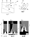
- Figure 1 is a schematic illustration of one embodiment of a device 10.
- the device 10 has a planar substrate 10p with a microchannel 15, a nanofunnel 20 and a nanochannel 30.
- the nanofunnel 20 has a narrow end 20n that defines a funnel-shaped entrance into a respective aligned nanochannel 30.
- the wide end of the funnel 20w can reside proximate a microchannel used for fluidic sample introduction.
- the nanochannel 30 can have a length that is much greater than the length of the funnel 20, typically at least three times greater and more typically greater than about 5 times, 6 times, 7 times, 8 times, 9 times, 10 times or even greater length.
- the nanofunnels 20 can have a relatively short length such as about 100 ⁇ m or less, typically between about 100 nm to about 50 ⁇ m, including about 75 ⁇ m, about 50 ⁇ m, about 25 ⁇ m, about 15 ⁇ m, about 10 ⁇ m, about 1 ⁇ m, about 500 nm, and about 100 nm or any number therebetween. In some embodiments, the length can be less than 100 nm, such as about 75 nm, about 50 nm, about 25 nm or less and any number therebetween.
- the device 10 can include at least one nanofunnel 20, but typically includes a plurality of spaced apart nanofunnels 20. Although shown as two spaced apart nanofunnels 20 1 , 20 2 , the device 10 can include more than two nanofunnels. As shown, each nanofunnel 20 1 , 20 2 can merge into a respective nanochannel 30 1 , 30 2 or connect other fluid structures.
- the nanofunnel 20 can be configured to have dimensions in both width and depth (also described as "height") that gradually decrease by over at least an order of magnitude along the transit path.
- the narrow end 20n with the smallest dimensions can be substantially equal to and aligned with those of a corresponding nanochannel 30 with which they can be (seamlessly) integrated.
- Figure 3A is a grayscale bitmap image used to pattern a funnel with gradually varying width and depth over its length 20 l .
- Figure 3B is a top view SEM (Scanning Electron Microscope) image of a funnel 20 and a first end of a corresponding nanochannel 30 milled into a quartz substrate using the bitmap 20bm shown in Figure 3A.
- Figure 3C is a top, end perspective view (tilted at 52 degrees) of the funnel and nanochannel shown in Figure 3B illustrating the varying depth (in the length direction).
- the funnel 20 decreases in size from about 1.5 ⁇ m x about 1.5 ⁇ m (width x depth) to about 25 nm x about 25 nm (width x depth).
- other funnel geometry and dimensions may be used.
- the funnels 20 can be configured to lower the threshold force needed to drive transport. This can be achieved by the gradual increase in the degree of confinement experienced by an analyte molecule as it moves along the length of the funnel 20. This effect, in combination with a force gradient that may partially be attributed to the funnel geometry, can effectively "precondition" the analyte molecule, resulting in a conformation conducive to threading into the nanochannel 30.
- Figures 4A-C and 5A illustrate a nanochannel 30 with a fluid reservoir 60 with an analyte 40 (DNA), and without a funnel 20, which can be used for mapping, sizing and sequencing DNA. See also, Levy et al., Chem Soc Rev 39 2010, 1133 ; Lagerqvist et al., Nano Lett, 6 2006, 779 , and U.S. Provisional Application Serial No. 61/384,738, filed September 21, 2010 (and corresponding pending PCT/US2011/052127 ) the contents of which are incorporated by reference as if recited in full herein.
- Figure 5B illustrates the device 10 with the nano funnel 20 that can provide an entry path for the analyte 40.
- FIG 6A illustrates a series of operations (A-C) that can be used to form devices 10 with at least one funnel 20 using milling, typically FIB milling. It is noted that the sequence of A and B may be reversed.
- the planar substrate 10p of the device 10 funnel(s) 20 can be processed to include one or more microfluidic channels 15 that can be prepared using standard photolithographic and etching techniques or other techniques (operation “A”).
- FIB milling can be used to form an interface with a funnel 20 and nanochannel 30 in the substrate 10p.
- the funnel and nanochannel 20, 30 can be seamless and connect to the channels 15 to be in fluid communication with the channels 15 and reservoirs 60 (operation "B").
- the device 10 can be a compact "chip”-like device with multiple nanofunnels 20 and nanochannels 30 and one or more associated reservoirs 60.
- the reservoir(s) 60 may have a short cylindrical configuration or other configuration and may be externally accessible ( Figure 6A ).
- the term "chip” refers to a substantially flat compact body with integrated fluidic structures.
- the chip can be any geometric shape but is typically polygonal, such as substantially square or substantially rectangular.
- the chip can be in different sizes but typically has an area that is less than about 10 in 2 (e.g., about 25 mm x 25 mm).
- FIG. 6A also illustrates that electrodes 70 can be attached to the device 10, typically with positive and negative polarity at spaced apart respective reservoirs 60 to drive the transport of the fluid analyte (e.g., molecule) through the fluidic structures as is well known.
- the fluid analyte e.g., molecule
- the device 10 can be configured for analyzing molecules, such as nucleic acids.
- the device 10 can be a nanofluidic chip comprising a plurality of nanofunnels 20, each connected to a respective nanochannel 20.
- the nanofunnels 20 and nanochannels 30 can have a smooth inner surface (from the milling process into the substrate).
- the nanofunnels 20 and the nanochannels 30 can include at least traces of implanted milling projectiles from a milling beam used to form the nanofunnels 20 and the nanochannels 30.
- the interface between a respective nanofunnel 20 and channel 30 can be seamless in that the narrow end of the funnel 20 can have the same dimensions as the nanochannel 30.
- the nanochannel 30 can have a constant width and depth over at least a major portion of its length and typically over its entire length.
- the nanochannel 30 can be formed during a single milling operation as continuation of the milling process used to form the nanofunnel 20 or vice versa (e.g., the nanochannel can be formed first and the nanofunnel can be a continuation of that process).
- the term "seamless" means that there is not a seam that adjoins the two features.
- the device 10 can have a planar substrate 10p of a variety of substrate materials, allowing device fabrication in glass, quartz, silicon, ceramics, metals, plastics, etc.
- FIB milling can be performed through a relatively thick (>100 nm) high quality metal film deposited on the top surface of the substrate. This metal film prevents charging during the milling process and allows milling of features with suitable tolerances and can allow critical dimensions that extend below 5 nm. See, e.g., U.S. Provisional Application Serial No. 61/384,738, filed September 21, 2010 and corresponding pending PCT/US2011/052127 , and Menard, L. D.; Ramsey, J. M., The fabrication of sub-5-nm nanochannels in insulating substrates using focused ion beam milling. Nano Lett. 2011, 11, 512 , the contents of which are incorporated by reference as if recited in full herein.
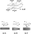
- Figures 7A-7C illustrates different exemplary geometric shaped funnel contours 20c.
- Figure 7A illustrates that the nanofunnel 20 has a convex contour 20cv.
- Figure 7B illustrates the funnel 20 has a straight line taper with walls tapering in at a (substantially) constant slope.
- Figure 7C show a nanofunnel 20 with a concave contour 20con.
- Figure 23 illustrates that the nanofunnel 20 can have a substantially parabolic relationship/shape.
- nanochannels 30 of a substantially constant depth can be fabricated by rastering the ion beam over a rectangular area or along a line, with each point in the rectangle or line exposed to the same ion dose. Deeper (funnel) channels can be milled by defining higher ion doses while shallower channels can be milled using lower ion doses.
- Figure 8A shows an example of an FIB milling device with a BMP milling mode where each pixel can define where and how long an ion beam dwells on the substrate 10p.
- Figure 8B illustrates an example of depth (nm) that can be set by dwell time (typically between about 1 ⁇ s to about 10 ms per pixel) with an appended gray scale graduated graph of dwell time resulting in increased depth.
- dwell time typically between about 1 ⁇ s to about 10 ms per pixel
- an appended gray scale graduated graph of dwell time resulting in increased depth typically between about 1 ⁇ s to about 10 ms per pixel.
- the fluidic network comprising a funnel 20 can be sealed by bonding a cover plate 50 (operation "C") on top of the substrate using one of several possible methods such as fusion, anodic, or adhesive bonding.
- FIG. 6A shows an embodiment where the funnels 20 can be configured so that both width and depth vary gradually and symmetrically around the long axis of the funnel 20.
- This configuration can be fabricated by milling identical funnel features and optionally a portion or all of the nanochannel 30, in both the top and bottom substrates 50, 10p , followed by bonding of the two substrates with precise alignment.
- prototypes of the device 10 were fabricated in quartz substrates because of quartz's suitability for micro fluidic and nanofluidic devices.
- FIB milling of nanofluidic structures can be extended to various hard and soft materials as described in the U.S. Provisional Application Serial No. 61/384,738, filed September 21, 2010 and corresponding pending PCT/US2011/052127 , which has been incorporated by reference.
- hard materials include, but are not limited to, substrates comprising one or combinations of: glass, quartz, silicon, and silicon nitride.
- the soft materials can have a low Young's Modulus value.
- elastomers and harder plastics and/or polymers can have a range between about 0.1-3000MPa.
- soft materials include, but are not limited to, polydimethylsiloxane (PDMS), polymethylmethacrylate (PMMA), and polyurethane.
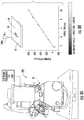
- a milling apparatus 200 can be configured to generate a desired shape of a nanofunnel 20 in a substrate 10.
- An electronic patterning file 200f (which can be provided in a number of manners including, for example, by one or more of an ASIC (Application Specific Integrated Circuit), an application (“APP"), a module and/or subdirectory file of a controller or digital signal processor) that can be held in the milling apparatus 200 or the milling apparatus 200.
- the apparatus 200 can be controlled or have access to at least one external (local or remote) device such as a processor with the electronic patterning file 200f that can generate a desired funnel shape in the substrate 10.
- the electronic patterning file 200f can also be distributed over various components and locations.
- the electronic patterning file 200f can define the dwell time per pixel of the milling beam 200b ( Figure 8B ) over X, Y coordinates, or other defined coordinate systems to generate a defined nanofunnel shape.
- the electronic patterning file 200f can be configured as selectable different patterning instructions correlated to one or more of the following: (i) different substrate materials; (ii) different nanofunnel shapes and/or dimensions; or (iii) different target analytes.
- the milling apparatus 200 can include a control circuit 200c that can communicate with at least one remote or local processor via a local area network (LAN), a wide area network (WAN) or via a global computer network, e.g., the Internet to obtain or use the electronic patterning file 200f.
- the milling apparatus 200 can be an FIB milling apparatus.
- a fabrication system 201 can comprise the apparatus 200 can include a control module or circuit 200c that can be onboard the apparatus or at least partially remote from the apparatus. If the latter, the control module or circuit 200c can reside totally or partially on a server 225 ( Figure 28 ).
- the server 225 can be provided using cloud computing which includes the provision of computational resources on demand via a computer network.
- FIB milling can be performed using a Helios NanoLab DualBeam Instrument (FEI Company) with a Ga + ion source operated at about 30kV.
- This instrument is capable of using bitmap image files (20bm, Figure 5A-7C ) to define a milling pattern.
- the x and y coordinates of the image define where the ion beam dwells during the scan, thus achieving milling, and the gray-scale value of the pixel (0 to 255) defines the length of time that the ion beam dwells on the region of the sample corresponding to the pixel.
- the operator or a default configuration of the apparatus 200 and/or the electronic patterning file 200f can define the maximum dwell time, t max .
- Figures 3B-3C show representative scanning electron microscopy (SEM) images of a funnel with varying depth and width interfaced to a nanofluidic channel.
- Figure 3A is an image of the original bitmap file 20bm used to mill the funnel and channel features shown in Figures 3B and 3C .
- FIG. 9A is a schematic illustration that shows an experimental setup where stained DNA solutions are added to the device reservoirs 60, DNA is electrokinetically driven via electrodes and electric field(s) through the nanochannels 30, and transport events are observed using fluorescence microscopy using a microscope 230.
- the inset shows a magnified view of the nanochannel array.
- the DNA was stained with an intercalating fluorescent dye (YOYO-1, Invitrogen) at a base pair to dye molecule ratio of 5:1. Fluorescence was excited by light from a mercury arc lamp passing through an excitation filter and a 100X oil-immersion plan apochromatic objective lens. Fluorescence from single molecules was collected through the 100X lens and imaged using an electron-multiplying CCD camera (Cascade II, Photometrics). This high sensitivity camera can collect images at frame rates up to 400 frames per second. Image analysis of individual, time-stamped frames provided information on single molecule dynamics such as molecular extension and the velocity of transport.
- YOYO-1 intercalating fluorescent dye
- the threshold field strength (in the nanochannels) required to drive DNA translocation through the nanochannels in this device was about 350 V/cm, or three-fold lower than the device without funneled entrances. Consequently, it was possible to record a greater number of frames for a single translocation event and analyze these frames to determine the dynamics of transport.
- a representative series of frames showing transport through one of the 25-nm nanochannels with a funneled entrance is shown in Figure 9B .
- the DNA molecule enters into the funnel where it slowly elongates into a configuration that then threads into the 25-nm nanochannel. In the absence of the confining funnel and at a comparable field strength, this threading process would likely progress too slowly to ensure translocation before the DNA molecule diffused away from the nanochannel entrance.
- Figure 9B illustrates a series of frames showing the transport of fluorescently-stained ⁇ -DNA molecules through a single 25-nm nanochannel with a funneled entrance.
- the inset SEM image shows the entrance of this nanochannel.
- the vertically oriented dashed lines indicate, from left to right, the entrance to the funnel, the funnel to nanochannel interface, and the other end of the nanochannel 30.
- funnel geometries can be selected to minimize the applied forces, making low velocity transport possible. This may be accomplished by calculating the force applied to the DNA molecule in the nanochannel under conditions where the entropic force of the molecule's gradual confinement in the funnel is balanced by the driving force in the funnel supplied by the applied voltage, pressure, or gravitational field. Additionally, the presence of the two opposing forces may result in a range of applied voltage, pressure, or centripetal force over which a DNA molecule can be trapped in the funnel indefinitely if appropriate funnel geometries are used.
- Optimal nanofunnel geometries can be determined by the theoretical modeling of DNA molecules subjected to the appropriate entropic and driving forces.
- DNA molecules are driven into and through the nanofunnels and nanochannels using an applied voltage. Similar modeling could be readily performed in which the driving force was an applied pressure or centripetal force, for example.
- Figures 10A-10C illustrate the information obtainable from these theoretical calculations.
- E min electric field strength
- the DNA molecule can be stably trapped in the nanofunnel 20.
- Theoretical modeling can determine the characteristic field strengths (E min , E c ) that define the stable trapping regime, the average position of a trapped DNA molecule (x i , x f ), its extended length (x f -x i ), and the critical voltage that must be applied to drive transport through the nanochannel (E c ).
- Low fields can momentarily trap DNA molecules but are insufficient to prevent their diffusive escape out of the nanofunnel 20 and away from the nanochannel 30.
- Intermediate fields E>E min , E ⁇ E c
- High fields can transport the DNA into and through the nanochannel 30.
- the values of the field strengths E min and E c are dependent on the shape and size of the nanofunnel and the size of the DNA molecule. For this reason, a theoretical understanding of DNA behavior in a nanofunnel, according to the examples shown, can be important for establishing these values a priori.
- Nanofunnel shapes can be configured to be optimal for different functions. For example, one nanofunnel can dramatically reduce the voltage required to drive transport into its associated nanochannel, resulting in low velocity DNA transport. The same nanofunnel may have a very limited range of voltages over which the DNA molecule is stably trapped. In contrast, a second nanofunnel can be optimized to have a large range of voltages over which trapping in the nanofunnel is stable. This second nanofunnel may require a higher critical voltage, however, to initiate DNA transport through the nanochannel.
- Figures 11A-D illustrate some elements of nanofunnel shape that have been investigated. The nanochannel width (w) and depth (d) vary with position along the nanofunnel's longitudinal axis (x) by the power law w,d ⁇ x ⁇ .
- Equation 1 can be used to define how the nanofunnel width and depth vary as a function of position along the nanofunnel raised to exponent " ⁇ ", again based on the desired nanofunnel operational characteristics.
- the width and depth are represented by a single variable, "D" (shown in Figure 11A ), which is the effective diameter of the narrow end of the nanofunnel (equivalent to the nanochannel cross-section dimensions, y is the width or depth of the nanofunnel at position x along the longitudinal (x) axis (also known as the symmetry or longitudinal centerline axis).
- y D x x 0 ⁇ , x > x 0
- Equation 1 is provided for example only as there are other equations of similar form that could be used to stretch or compress the nanofunnel while maintaining the same alpha.
- any suitable power law equation can be used to select dimensions for different desired exponents ( ⁇ ) according to what behavior or molecule is targeted for analysis, based on the proportional relationship: y ⁇ x ⁇ .
- y is understood to represent either of the dimensions width or depth.
- the width and depth may be defined by the same function of x, yielding a nanofunnel with an aspect ratio (depth:width) of 1 along its entire length.
- the width and depth may be defined by different functions of x, yielding a nanofunnel with an aspect ratio other than 1 (e.g., 0.1, 0.2, 0.5, 2, 4) along its entire length or an aspect ratio that varies along the nanofunnel's length.
- the nanofunnel 20 can have a shape defined by a concatenation of functions (y 1 , y 2 , y 3 , ...) where the width and depth of the nanofunnel are defined by y 1 between axial coordinates x 0 and x 1 , by y 2 between axial coordinates x 1 and x 2 , by y 3 between axial coordinates x 2 and x 3 , and so on.
- Each segment of the nanofunnel can be seamlessly or discontinuously connected to its neighboring segments and the narrow end of the nanofunnel can be seamlessly connected to a corresponding aligned nanochannel or microchannel.
- the concatenated nano funnels can consist of 2 to 10 segments in some embodiments or can form long fluidic conduits consisting of up to hundreds or thousands of segments in other embodiments.
- the funnel 20 can have a configuration where the exponent ⁇ can itself be a function of axial position x. This can create more complicated funnel shapes.
- Figure 11E shows a simple example with an exemplary function where the exponent alpha is a function of x.
- nanofunnels can be configured as a series of segments where the dimensions in each segment are defined by a different geometric relationship and where the segments are connected seamlessly ( Figure 11F ) or discontinuously ( Figure 11G ).
- Figure 11A maps an idealized cylindrical funnel onto a coordinate axis to illustrate the functional form, y ⁇ x ⁇ . Funnels for which ⁇ 1 are convex, while those for which ⁇ >1 are concave.
- Figure 11B shows a series of funnel shapes having different ⁇ exponent values.
- FIGS 11C, 11D show how the voltage, V, varies along the length of a nanofunnel when ⁇ 0.5 ( Figure 11C ) and when ⁇ >0.5 ( Figure 11D ). In these plots, a larger slope in the curve corresponds to a higher electric field at the position, x. When ⁇ 0.5 ( Figure 11C ), the voltage increases linearly along the entire nanofunnel length and can do so indefinitely.
- Figure 12 shows one important way in which the properties of DNA can affect the operational parameters of trapping and critical transport voltages. Due to the voltage profile in a nanofunnel with ⁇ 0.5, the electrostatic force on the trailing end of the DNA molecule acts like a piston, compressing the leading end of the molecule, pushing it towards the nanochannel entrance, and lowering the critical voltage needed to drive transport.
- Figure 13A compares theory (lines) and simulation results (markers) describing the position of a DNA molecule's leading end (x i ) as a function of applied voltage (proportional to Eo, the electric field magnitude in the nanochannel).
- Figure 14 shows a comparison of theory and simulations describing the dependence of the critical electric field required to drive transport through the nanochannel on the power law exponent, ⁇ .
- the dimensionless variable of the plot ordinate is the critical field with the nanofunnel E c f , normalized by the critical field necessary to drive transport through a nanochannel with no funnel, E c .
- FIG. 15A Fluorescence images were recorded ( Figure 15B ) and reduced to an intensity profile ( Figure 15C ) characterizing DNA length and position.
- Figure 15D shows a time series of these frames highlighting the thermal fluctuations in the molecule's length and position.
- Figures 16 and 17 are graphs of the voltage dependence of trapping position for two DNA molecules having different contour lengths ( ⁇ -phage, ⁇ 20 ⁇ m long, and T4-phage DNA, ⁇ 70 ⁇ m long) in an electrophoresis buffer and in some instances, as indicated, containing 2% by weight of a low molecular weight polymer, polyvinylpyrrolidone (PVP).
- PVP polyvinylpyrrolidone
- Figure 18 is a related graph that illustrates the relationship between the voltage-dependent properties of DNA length and trapping position. These two values are correlated because the greater confinement experienced by the DNA molecule as it is driven deeper into the funnel results in greater extension. The variances in these parameters provide a measure of the trap stability vis-à-vis thermal fluctuations. Each data point in Figures 16-18 represents the average of over 20,000 measurements collected over about 30 minutes.
- funnels 20 can facilitate macromolecule capture, trapping, and transport through nanochannels 30 having critical dimensions smaller than the radius of gyration of the molecule.
- the threshold force needed to drive translocation By lowering the threshold force needed to drive translocation, greater control over molecular transport dynamics may be achieved.
- channels 30 with nanoscale dimensions in width and depth confinement of the macromolecule in both of these dimensions is disfavored by an entropic energy barrier. Therefore, the optimal funnel geometry can provide a gradual increase in confinement in both dimensions. This can be achieved by patterning funnels using FIB milling in which the lateral dimensions and shape of the funnel are controlled by the pattern over which the beam is rastered.
- the depth of the funnel is controlled by varying the dwell time of the ion beam, milling deeper features at the funnel mouth and gradually shallower features towards the intersection of the funnel and nanochannel.
- the introduction of such funnels at the entrance to nanochannels has been predicted theoretically and verified experimentally to reduce the voltage that must be applied to electrokinetically drive double-stranded DNA through long FIB-milled nanochannels. Additionally, given appropriate funnel geometries and capture forces, single molecules can be stably trapped and investigated for a desired length of time.
- the devices 10 and/or nanofunnels 20 can be configured to analyze a DNA molecule, a protein, a fluorescently stained molecule, and optionally the analyte molecule can be been modified in any way to provide or enhance analyzing the molecule in a respective nanochannel 20.
- FIB milling to fabricate features with control in all three dimensions provides an ultimate degree of flexibility in funnel design.
- a macromolecule can be gradually driven through an FIB-milled funnel directly into a nanochannel, transitioning from an unconfined to a highly confined state. This gradual transition can result in translocations occurring at low molecular velocities in which the molecule preferentially enters the nanochannel in an unfolded, extended state.
- funnels to facilitate the threading of macromolecules into nanochannels lowers the threshold force needed to drive translocation and thus lowers the transport velocity, which is expected to enable more precise optical and electrical measurements on single confined molecules.
- One example is the sequencing of DNA molecules in a nanochannel interfaced to opposed tunneling probes in which base calling is achieved by measuring the unique tunneling currents through the individual nucleotides.
- Such a funnel could also be used in isolation (without interfacing it to a long nanochannel) as a conduit between two microchannels and serving as a stochastic sensor. Translocations through the funnel could be monitored optically (e.g. fluorescently stained molecules) and/or electrically (e.g., axial ionic current).
- a potential advantage to this geometry is the seamless integration of microfluidic and nanofluidic components on a single layer device, in contrast to stacked devices that integrate microfluidic channels and nanoporous membranes.
- Funnels 20 in which both the width and depth vary gradually are also believed to be suitable, potentially ideal, platforms upon which to study the physical properties of flexible or deformable macromolecules. Because the FIB milled nanochannels and nanofunnels are easily interfaced with other fluidic components on a single chip their use can be integrated with other technologies such as flow injection, separations in microfluidic channels, and single cell lysis.
- Nanofluidic implementations with nanochannels of these critical dimensions and quality are well suited for a number of applications including single molecule detection and identification, confinement and manipulation of biopolymers, biological assays, restriction mapping of polynucleotides, DNA sizing, physical methods of genomic sequencing, and fundamental studies of the physics of confinement.
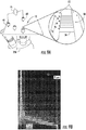
- Figure 19 is a schematic illustration showing experimental evaluations of translocation event frequency for DNA molecules electrokinetically driven through the nanochannel from either the funnel side (right to left in Figure 19 ) or the channel side (left to right in Figure 19 ).
- Figure 20 shows the experimental results of the two experiments shown in Figure 19 .
- the linear increase of translocation event frequency with applied voltage at higher voltages indicates that voltages in this range exceed the entropic barrier value.
- the exponential region of the data seen at low voltages indicates the presence of an entropic barrier. This barrier is not observed in translocations originating from the funnel side.
- Figure 21 is a fluorescence microscopy image that shows further evidence for the existence of an energy barrier to translocation from the channel side.
- the nanofunnels differ in the exponent, ⁇ , that defines their shape.
- ⁇ that defines their shape.
- the electric field in the funnels and nanochannels can be compared.
- the nanochannel and nanofunnel shape can be precisely determined using atomic force microscopy ( Figures 22A, 22B ), SEM imaging ( Figures 3B, 3C , 7A, 7B , 7C , 23 ), and ion beam tomography, for example.
- the optimal shape(s) may change for macromolecules having different physical properties, systems with different polymer-solvent intermolecular interactions, and driving forces with different flow profiles, all parameters that can be investigated theoretically.
- Figure 23 illustrates a bitmap image 20bm used to create a corresponding FIB milled funnel 20 and nanochannel 30 (SEM image) with a length of about 22 ⁇ m and a graph of an AFM (Atomic Force microscopy) image of width ( ⁇ m) versus length ( ⁇ m).
- SEM image a bitmap image 20bm used to create a corresponding FIB milled funnel 20 and nanochannel 30
- AFM Anatomic Force microscopy
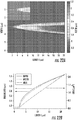
- Figure 24 is a graph showing a parabolic relationship of depth and width over a length of the nanofunnel 20 according to some embodiments of the present invention. That is, the nanofunnel(s) 20 can be configured to have both width and depth dimensions that vary in a parabolic, linear manner over its length according to some embodiments of the present invention.
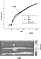
- Figure 25 shows AFM images of nanofunnels defined by a power law function with ⁇ values of 0, 0.5, and 1. Devices incorporating such nanofunnels were used to determine the results represented in the table above.
- the gray or color scale labeled "Depth ( ⁇ m)" on the right hand side of the figure shows how the intensities of the nanofunnel profiles on the left hand side of the figure correspond to nanofunnel depth.
- Figure 26A illustrates the comparison between the experimentally determined positions of the leading and tailing ends of a trapped ⁇ -phage DNA molecule.
- Figure 26B illustrates the comparison between the experimentally determined positions of the leading and tailing ends of a trapped T4-phage DNA molecule.
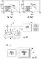
- Figure 27 is a schematic illustration of an analysis system 100 which includes at least one device 10 with at least one nanofunnel 20, electrodes 70 and a control circuit 101 with a funnel applied voltage mode and a channel applied voltage mode, the funnel mode configured to apply a larger voltage than the channel mode.
- Figure 28 is a schematic illustration of a fabrication system 201 with a milling apparatus 200 and a circuit 200c with a nanofunnel patterning file 200f which can be totally onboard the apparatus 200, partially onboard the apparatus 200 or remote from the apparatus such as in one or more servers 225.
Claims (9)
- Procédé d'analyse d'un analyte, comprenant :la fourniture d'une puce avec au moins un nano-entonnoir (20) qui se transforme en un nanocanal (30) correspondant ;l'application d'une première tension pour amener un analyte à s'écouler dans un nano-entonnoir fluidique (20) ; puisl'application d'une seconde tension, plus faible, pour amener l'analyte à s'écouler dans un nanocanal (30) correspondant ; etl'analyse électronique de la molécule dans le nano-entonnoir et/ou le nanocanal.
- Procédé selon la revendication 1, comprenant la détermination de l'identification moléculaire de l'analyte, de la longueur de l'analyte ou d'une cartographie localisée de la fonctionnalisation en fonction des données de l'étape d'analyse.
- Procédé selon la revendication 1 ou la revendication 2, dans lequel l'étape d'application est réalisée de manière à ce que l'écoulement dans le nanocanal soit à une faible vélocité de < 0,1 mm/s.
- Procédé selon l'une quelconque des revendications précédentes, dans lequel l'étape d'analyse comprend la détermination d'informations sur la séquence d'ADN.
- Procédé selon l'une quelconque des revendications précédentes, dans lequel le au moins un nano-entonnoir (20) est constitué d'une série concaténée de parties dans lesquelles une dimension de largeur et de profondeur respective varie dans une relation géométrique définie sur toute la longueur de chaque partie, dans lequel la largeur et la profondeur de chaque partie sont définies par une fonction géométrique différente, et dans lequel les parties avoisinantes sont reliées sans coupure ou de manière discontinue.
- Procédé selon l'une quelconque des revendications précédentes, dans lequel le au moins un nano-entonnoir (20) comprend au moins une partie avec au moins un des éléments suivants :un contour parabolique ;un contour convexe ;un contour concave ; etdes parois qui forment un angle vers l'intérieur à une pente constante.
- Procédé selon l'une quelconque des revendications précédentes, dans lequel le au moins un nano-entonnoir (20) comprend une pluralité de nano-entonnoirs, chacun ayant une longueur qui se situe entre environ 1 µm à environ 100 µm.
- Procédé selon l'une quelconque des revendications précédentes, dans lequel les dimensions de largeur et de profondeur du ou de chaque nano-entonnoir (20) varient, éventuellement dans une relation géométrique définie, sur toute la longueur du nano-entonnoir pour modifier une taille transversale de l'entonnoir par au moins un facteur de deux de l'extrémité large à l'extrémité étroite.
- Procédé selon l'une quelconque des revendications précédentes, dans lequel le ou chaque nano-entonnoir (30) a une une largeur et une profondeur constantes, et dans lequel l'extrémité étroite d'un nano-entonnoir respectif a des dimensions de largeur et de profondeur qui correspondent à une dimension de largeur et de profondeur d'un nanocanal correspondant aligné.
Priority Applications (1)
| Application Number | Priority Date | Filing Date | Title |
|---|---|---|---|
| EP19187579.8A EP3591408A1 (fr) | 2012-02-10 | 2013-02-07 | Dispositifs avec nano-entonnoirs fluidiques, procédés associés, systèmes de fabrication et d'analyse |
Applications Claiming Priority (2)
| Application Number | Priority Date | Filing Date | Title |
|---|---|---|---|
| US201261597364P | 2012-02-10 | 2012-02-10 | |
| PCT/US2013/025078 WO2013119765A1 (fr) | 2012-02-10 | 2013-02-07 | Dispositifs à nano-entonnoirs fluidiques, procédés associés, systèmes de fabrication et d'analyse |
Related Child Applications (2)
| Application Number | Title | Priority Date | Filing Date |
|---|---|---|---|
| EP19187579.8A Division EP3591408A1 (fr) | 2012-02-10 | 2013-02-07 | Dispositifs avec nano-entonnoirs fluidiques, procédés associés, systèmes de fabrication et d'analyse |
| EP19187579.8A Division-Into EP3591408A1 (fr) | 2012-02-10 | 2013-02-07 | Dispositifs avec nano-entonnoirs fluidiques, procédés associés, systèmes de fabrication et d'analyse |
Publications (3)
| Publication Number | Publication Date |
|---|---|
| EP2812708A1 EP2812708A1 (fr) | 2014-12-17 |
| EP2812708A4 EP2812708A4 (fr) | 2015-09-30 |
| EP2812708B1 true EP2812708B1 (fr) | 2019-09-04 |
Family
ID=48947986
Family Applications (2)
| Application Number | Title | Priority Date | Filing Date |
|---|---|---|---|
| EP13746055.6A Active EP2812708B1 (fr) | 2012-02-10 | 2013-02-07 | Procédé d'analyse d'un analyte avec des nano-entonnoirs fluidiques |
| EP19187579.8A Withdrawn EP3591408A1 (fr) | 2012-02-10 | 2013-02-07 | Dispositifs avec nano-entonnoirs fluidiques, procédés associés, systèmes de fabrication et d'analyse |
Family Applications After (1)
| Application Number | Title | Priority Date | Filing Date |
|---|---|---|---|
| EP19187579.8A Withdrawn EP3591408A1 (fr) | 2012-02-10 | 2013-02-07 | Dispositifs avec nano-entonnoirs fluidiques, procédés associés, systèmes de fabrication et d'analyse |
Country Status (4)
| Country | Link |
|---|---|
| US (2) | US9989515B2 (fr) |
| EP (2) | EP2812708B1 (fr) |
| JP (3) | JP6339024B2 (fr) |
| WO (1) | WO2013119765A1 (fr) |
Cited By (1)
| Publication number | Priority date | Publication date | Assignee | Title |
|---|---|---|---|---|
| US11568958B2 (en) | 2017-12-29 | 2023-01-31 | Clear Labs, Inc. | Automated priming and library loading device |
Families Citing this family (29)
| Publication number | Priority date | Publication date | Assignee | Title |
|---|---|---|---|---|
| US9180453B2 (en) | 2008-08-15 | 2015-11-10 | University Of Washington | Method and apparatus for the discretization and manipulation of sample volumes |
| NZ610129A (en) | 2010-10-04 | 2014-08-29 | Genapsys Inc | Systems and methods for automated reusable parallel biological reactions |
| US9926596B2 (en) | 2011-05-27 | 2018-03-27 | Genapsys, Inc. | Systems and methods for genetic and biological analysis |
| US11053535B2 (en) | 2011-09-12 | 2021-07-06 | The University Of North Carolina At Chapel Hill | Devices with a fluid transport nanochannel intersected by a fluid sensing nanochannel and related methods |
| CN104105797B (zh) | 2011-12-01 | 2016-08-31 | 吉纳普赛斯股份有限公司 | 用于高效电子测序与检测的系统和方法 |
| US9989515B2 (en) | 2012-02-10 | 2018-06-05 | The University Of North Carolina At Chapel Hill | Devices with fluidic nanofunnels, associated methods, fabrication and analysis systems |
| WO2014134095A1 (fr) | 2013-02-28 | 2014-09-04 | The University Of North Carolina At Chapel Hill | Dispositifs nanofluides dotés de composants intégrés et conçus pour contrôler la capture, le piégeage et le transport de macromolécules et procédés d'analyse connexes |
| US9255288B2 (en) | 2013-03-13 | 2016-02-09 | The University Of North Carolina At Chapel Hill | Nanofluidic devices for the rapid mapping of whole genomes and related systems and methods of analysis |
| US9809852B2 (en) | 2013-03-15 | 2017-11-07 | Genapsys, Inc. | Systems and methods for biological analysis |
| US11219896B2 (en) | 2013-06-25 | 2022-01-11 | University Of Washington Through Its Center For Commercialization | Self-digitization of sample volumes |
| US20150037787A1 (en) * | 2013-07-31 | 2015-02-05 | International Business Machines Corporation | Polynucleotide configuration for reliable electrical and optical sensing |
| EP3792921A1 (fr) * | 2013-12-11 | 2021-03-17 | Genapsys, Inc. | Systèmes et procédés d'analyse et de calcul biologiques |
| EP3132060B1 (fr) | 2014-04-18 | 2019-03-13 | Genapsys Inc. | Procédés et systèmes pour l'amplification d'acide nucléique |
| WO2016069624A1 (fr) * | 2014-10-27 | 2016-05-06 | Board Of Regents, The University Of Texas System | Plate-forme d'imagerie à haut débit |
| US9606082B2 (en) | 2015-05-11 | 2017-03-28 | The University Of North Carolina At Chapel Hill | Pressure driven microfluidic injection for chemical separations |
| US10734216B2 (en) | 2015-05-11 | 2020-08-04 | The University Of North Carolina At Chapel Hill | Pressure driven fluidic injection for chemical separations by electrophoresis |
| US10471428B2 (en) | 2015-05-11 | 2019-11-12 | The University Of North Carolina At Chapel Hill | Fluidic devices with nanoscale manifolds for molecular transport, related systems and methods of analysis |
| US9255905B1 (en) | 2015-05-11 | 2016-02-09 | The University Of North Carolina At Chapel Hill | Pressure driven microfluidic injection for chemical separations |
| JP6868289B2 (ja) | 2015-07-07 | 2021-05-12 | ユニバーシティ オブ ワシントンUniversity of Washington | サンプルの自己デジタル化のためのシステム、方法、およびデバイス |
| US9728387B2 (en) | 2015-10-20 | 2017-08-08 | The University Of North Carolina At Chapel Hill | Solid phase extraction with capillary electrophoresis |
| WO2017095813A1 (fr) | 2015-11-30 | 2017-06-08 | Intabio, Inc. | Dispositifs et procédés de caracterisation d'échantillon |
| CN109790575A (zh) | 2016-07-20 | 2019-05-21 | 吉纳普赛斯股份有限公司 | 用于核酸测序的系统和方法 |
| KR102446129B1 (ko) * | 2016-10-03 | 2022-09-22 | 젠비다 테크놀로지 컴퍼니 리미티드 | 분자의 식별 및 분석을 위한 장치 및 방법. |
| CA3076378A1 (fr) | 2017-09-21 | 2019-03-28 | Genapsys, Inc. | Systemes et procedes de sequencage d'acides nucleiques |
| US20190210016A1 (en) * | 2018-01-05 | 2019-07-11 | Genturi, Inc. | Duty cycle optimization in single-molecule detection |
| SG11202007188RA (en) | 2018-01-29 | 2020-08-28 | Intabio Inc | Devices, methods and kits for sample characterization |
| CN112534549A (zh) | 2018-05-31 | 2021-03-19 | 因塔生物公司 | 用于微流体系统与质谱联用的软件 |
| US11285484B2 (en) | 2019-08-12 | 2022-03-29 | Intabio, Llc | Multichannel isoelectric focusing devices and high voltage power supplies |
| CN112791755B (zh) * | 2021-03-31 | 2021-07-02 | 苏州大学 | 多层微流控芯片封装器件、多层微流控芯片及其应用 |
Citations (2)
| Publication number | Priority date | Publication date | Assignee | Title |
|---|---|---|---|---|
| WO2001013088A1 (fr) * | 1999-08-13 | 2001-02-22 | U.S. Genomics, Inc. | Procede et appareil d'etirage de polymeres |
| WO2003106693A2 (fr) * | 2002-01-01 | 2003-12-24 | Princeton University | Structures de gradient interfaçant des elements microfluidiques et des elements nanofluidiques, leurs procedes de fabrication et d'utilisation |
Family Cites Families (94)
| Publication number | Priority date | Publication date | Assignee | Title |
|---|---|---|---|---|
| US5498392A (en) | 1992-05-01 | 1996-03-12 | Trustees Of The University Of Pennsylvania | Mesoscale polynucleotide amplification device and method |
| US5296116A (en) | 1992-06-17 | 1994-03-22 | Beckman Instruments, Inc. | Capillary electrophoresis using time-varying field strength |
| US6001229A (en) | 1994-08-01 | 1999-12-14 | Lockheed Martin Energy Systems, Inc. | Apparatus and method for performing microfluidic manipulations for chemical analysis |
| US7775368B2 (en) | 1995-04-03 | 2010-08-17 | Wisconsin Alumni Research Foundation | Micro-channel long molecule manipulation system |
| US5872010A (en) | 1995-07-21 | 1999-02-16 | Northeastern University | Microscale fluid handling system |
| US6074827A (en) | 1996-07-30 | 2000-06-13 | Aclara Biosciences, Inc. | Microfluidic method for nucleic acid purification and processing |
| US5858187A (en) | 1996-09-26 | 1999-01-12 | Lockheed Martin Energy Systems, Inc. | Apparatus and method for performing electrodynamic focusing on a microchip |
| US6316213B1 (en) | 1997-03-19 | 2001-11-13 | The Board Of Trustees Of The University Of Arkansas | Methods for the early diagnosis of ovarian, breast and lung cancer |
| US6235471B1 (en) | 1997-04-04 | 2001-05-22 | Caliper Technologies Corp. | Closed-loop biochemical analyzers |
| US7033474B1 (en) | 1997-04-25 | 2006-04-25 | Caliper Life Sciences, Inc. | Microfluidic devices incorporating improved channel geometries |
| US6969488B2 (en) | 1998-05-22 | 2005-11-29 | Solexa, Inc. | System and apparatus for sequential processing of analytes |
| US5900130A (en) | 1997-06-18 | 1999-05-04 | Alcara Biosciences, Inc. | Method for sample injection in microchannel device |
| US5965410A (en) | 1997-09-02 | 1999-10-12 | Caliper Technologies Corp. | Electrical current for controlling fluid parameters in microchannels |
| DE19826020C2 (de) | 1998-06-10 | 2000-11-02 | Max Planck Gesellschaft | Vorrichtung und Verfahren zur miniaturisierten, hochparallelen elektrophoretischen Trennung |
| US6627446B1 (en) | 1998-07-02 | 2003-09-30 | Amersham Biosciences (Sv) Corp | Robotic microchannel bioanalytical instrument |
| US6790671B1 (en) | 1998-08-13 | 2004-09-14 | Princeton University | Optically characterizing polymers |
| EP1157144A4 (fr) | 1999-01-13 | 2010-04-28 | Cornell Res Foundation Inc | Fabrication de structures fluidiques monolithiques |
| US6500323B1 (en) | 1999-03-26 | 2002-12-31 | Caliper Technologies Corp. | Methods and software for designing microfluidic devices |
| US6690004B2 (en) | 1999-07-21 | 2004-02-10 | The Charles Stark Draper Laboratory, Inc. | Method and apparatus for electrospray-augmented high field asymmetric ion mobility spectrometry |
| US6524456B1 (en) | 1999-08-12 | 2003-02-25 | Ut-Battelle, Llc | Microfluidic devices for the controlled manipulation of small volumes |
| US6762059B2 (en) | 1999-08-13 | 2004-07-13 | U.S. Genomics, Inc. | Methods and apparatuses for characterization of single polymers |
| US6592733B1 (en) | 1999-11-12 | 2003-07-15 | Motorola, Inc. | Capillary electrophoresis devices incorporating optical waveguides |
| AU2450801A (en) | 1999-12-30 | 2001-07-16 | Advion Biosciences, Inc. | Multiple electrospray device, systems and methods |
| US6537433B1 (en) | 2000-03-10 | 2003-03-25 | Applera Corporation | Methods and apparatus for the location and concentration of polar analytes using an alternating electric field |
| US6994826B1 (en) | 2000-09-26 | 2006-02-07 | Sandia National Laboratories | Method and apparatus for controlling cross contamination of microfluid channels |
| US20050196746A1 (en) * | 2001-03-24 | 2005-09-08 | Jia Xu | High-density ion transport measurement biochip devices and methods |
| US20020190204A1 (en) | 2001-06-04 | 2002-12-19 | Bruker Daltonics, Inc. | Systems and method of a gated electrospray interface with variable flow rate for high throughput mass spectrometric analysis |
| GB0116384D0 (en) | 2001-07-04 | 2001-08-29 | Diagnoswiss Sa | Microfluidic chemical assay apparatus and method |
| CA2454570C (fr) | 2001-07-25 | 2016-12-20 | The Trustees Of Princeton University | Reseaux de nanocanaux, leurs preparation et utilisation dans l'analyse macromoleculaire a rendement eleve |
| EP1436424A4 (fr) | 2001-09-18 | 2005-11-16 | Us Genomics Inc | Marquage differentiel de polymeres pour une analyse lineaire a haute resolution |
| US6803568B2 (en) | 2001-09-19 | 2004-10-12 | Predicant Biosciences, Inc. | Multi-channel microfluidic chip for electrospray ionization |
| US7220345B2 (en) | 2001-10-18 | 2007-05-22 | The Board Of Trustees Of The University Of Illinois | Hybrid microfluidic and nanofluidic system |
| JP2003166934A (ja) | 2001-11-29 | 2003-06-13 | Hamamatsu Photonics Kk | 分別セルおよび光学的微小物質の分別装置 |
| EP2581739B1 (fr) | 2002-03-05 | 2015-11-04 | Caliper Life Sciences, Inc. | Procédé de separation microfluidique avec commande combinée de pression et de voltage |
| WO2003080829A1 (fr) * | 2002-03-26 | 2003-10-02 | Jun Kikuchi | Dispositif de piegeage/liberation d'adn utilisant un canal, et procede de piegeage et de liberation d'adn |
| JP3866183B2 (ja) | 2002-11-01 | 2007-01-10 | Asti株式会社 | バイオチップ |
| WO2004113898A1 (fr) * | 2003-05-19 | 2004-12-29 | Protasis Corporation | Dispositifs d'electrophorese et procedes de concentration d'analytes charges |
| US20060240573A1 (en) * | 2003-07-29 | 2006-10-26 | Lamdagen, Llc | Optical system including nanostructures for biological or chemical sensing |
| US20050103713A1 (en) | 2003-07-30 | 2005-05-19 | Ramsey J. M. | Devices with small-scale channels and the fabrication thereof by etching |
| US20050023156A1 (en) | 2003-07-30 | 2005-02-03 | Ramsey J. Michael | Nanostructured material transport devices and their fabrication by application of molecular coatings to nanoscale channels |
| JP2005102619A (ja) * | 2003-09-30 | 2005-04-21 | Toshiba Corp | 細胞変態装置及び細胞変態方法 |
| US7465381B2 (en) | 2004-01-22 | 2008-12-16 | Stc.Unm | Electrokinetic molecular separation in nanoscale fluidic channels |
| JP2005241255A (ja) | 2004-02-24 | 2005-09-08 | Mari Tabuchi | 電気泳動法 |
| US20060060769A1 (en) | 2004-09-21 | 2006-03-23 | Predicant Biosciences, Inc. | Electrospray apparatus with an integrated electrode |
| US7527970B2 (en) | 2004-10-15 | 2009-05-05 | The United States Of America As Represented By The Department Of Health And Human Services | Method of identifying active chromatin domains |
| US7947485B2 (en) | 2005-06-03 | 2011-05-24 | Hewlett-Packard Development Company, L.P. | Method and apparatus for molecular analysis using nanoelectronic circuits |
| US20060278879A1 (en) | 2005-06-09 | 2006-12-14 | Cabot Microelectronics Corporation | Nanochannel device and method of manufacturing same |
| WO2007011622A2 (fr) * | 2005-07-18 | 2007-01-25 | U.S. Genomics, Inc. | Procedes microfluidiques et dispositifs de preparation et d'analyse d'echantillons |
| US7988839B2 (en) | 2005-09-20 | 2011-08-02 | University Of Louisville Research Foundation, Inc. | Capillary electrophoresis systems and methods |
| JP2007149861A (ja) | 2005-11-25 | 2007-06-14 | Seiko Epson Corp | イオンミリング装置 |
| WO2007065025A2 (fr) | 2005-11-29 | 2007-06-07 | Wisconsin Alumni Research Foundation | Procede d'analyse d'adn au moyen de micro/nano-canaux |
| TWI274040B (en) | 2005-12-23 | 2007-02-21 | Ind Tech Res Inst | Microfluidic device and method of manufacturing the same |
| US8759811B2 (en) * | 2006-02-14 | 2014-06-24 | Raytheon Company | Particle encapsulated nanoswitch |
| JP2007278906A (ja) * | 2006-04-07 | 2007-10-25 | National Institute For Materials Science | ナノギャップアレイ及びそれを用いた生体高分子の診断方法 |
| WO2007127631A2 (fr) | 2006-04-28 | 2007-11-08 | The Regents Of The University Of California | Emetteurs multi-buses monolithiques pour spectrometrie de masse en mode nano-electrospray |
| AU2007338862B2 (en) * | 2006-07-19 | 2014-02-06 | Bionano Genomics, Inc. | Nanonozzle device arrays: their preparation and use for macromolecular analysis |
| US7744762B2 (en) | 2006-08-24 | 2010-06-29 | Virginia Tech Intellectual Properties, Inc. | Microfluidic devices and methods facilitating high-throughput, on-chip detection and separation techniques |
| US7771790B2 (en) | 2006-08-30 | 2010-08-10 | Tokyo Electron Limited | Method and system for fabricating a nano-structure |
| JP5491378B2 (ja) | 2007-03-28 | 2014-05-14 | バイオナノ ジェノミックス、インク. | ナノチャネルアレイを用いた巨大分子解析方法 |
| WO2008134363A1 (fr) | 2007-04-25 | 2008-11-06 | The Regents Of The University Of Michigan | Nanocanaux élastomères réglables pour manipulation nanofluidique |
| US8557707B2 (en) | 2007-04-30 | 2013-10-15 | Technion Research And Development Foundation Ltd. | Focused ion beam deep nano-patterning apparatus and method |
| US20090115094A1 (en) | 2007-05-29 | 2009-05-07 | Chou Stephen Y | Methods for making continuous nanochannels |
| EP2014761B1 (fr) * | 2007-06-22 | 2016-09-28 | Sony Deutschland GmbH | Dispositif de traitement d'analyse et procédé de traitement et/ou détection d'une analyse à l'aide de ce dispositif |
| GB0717150D0 (en) | 2007-09-04 | 2007-10-17 | Univ Warwick | Apparatus and method |
| WO2009045473A2 (fr) | 2007-10-02 | 2009-04-09 | President And Fellows Of Harvard College | Synthèse de nanotubes de carbone pour dispositifs à nanopores |
| US8951731B2 (en) | 2007-10-15 | 2015-02-10 | Complete Genomics, Inc. | Sequence analysis using decorated nucleic acids |
| WO2009120642A1 (fr) | 2008-03-26 | 2009-10-01 | Massachusetts Institute Of Technology | Procédés de fabrication de dispositifs de concentration électrocinétiques |
| KR20170094003A (ko) | 2008-06-06 | 2017-08-16 | 바이오나노 제노믹스, 인크. | 통합 나노유체 분석 장치, 제작 방법 및 분석 기술 |
| WO2010044932A2 (fr) | 2008-07-11 | 2010-04-22 | Cornell University | Canaux nanofluidiques avec capteurs de charge intégrés et procédés fonctionnant à l'aide de ces derniers |
| US8753868B2 (en) | 2008-08-04 | 2014-06-17 | General Electric Company | Method and system for selective isolation of target biological molecules in a general purpose system |
| US8262879B2 (en) | 2008-09-03 | 2012-09-11 | Nabsys, Inc. | Devices and methods for determining the length of biopolymers and distances between probes bound thereto |
| WO2010042007A1 (fr) | 2008-10-10 | 2010-04-15 | Jonas Tegenfeldt | Procédé de cartographie du rapport at/gc local sur la longueur d'un fragment d'adn |
| US9810680B2 (en) | 2009-04-16 | 2017-11-07 | Nanonex Corporation | Nanogap electronic detector for measuring properties of a biomolecule stretched in a nanochannel, and method thereof |
| US8246799B2 (en) | 2009-05-28 | 2012-08-21 | Nabsys, Inc. | Devices and methods for analyzing biomolecules and probes bound thereto |
| WO2011017681A2 (fr) | 2009-08-06 | 2011-02-10 | Cornell University | Dispositif et procédé d'analyse moléculaire |
| WO2011022650A2 (fr) | 2009-08-21 | 2011-02-24 | Cornell University | Dispositifs de nanofiltres utilisant des interfaces élastomères de jonction entre des microcanaux et des nanocanaux, et procédés utilisant ces dispositifs |
| US8748091B2 (en) | 2009-12-18 | 2014-06-10 | The Board Of Trustees Of The University Of Illinois | Characterizing stretched polynucleotides in a synthetic nanopassage |
| US8940148B2 (en) | 2010-06-22 | 2015-01-27 | International Business Machines Corporation | Nano-fluidic field effective device to control DNA transport through the same |
| US9139426B2 (en) | 2010-09-21 | 2015-09-22 | The University Of North Carolina At Chapel Hill | Methods, systems and devices for forming nanochannels |
| JP2012093338A (ja) | 2010-09-30 | 2012-05-17 | Fujifilm Corp | 生体分子検出装置および生体分子検出方法 |
| GB201017905D0 (en) | 2010-10-25 | 2010-12-01 | Mir Kalim U | Preparation and analysis of samples |
| US20120193231A1 (en) | 2011-01-28 | 2012-08-02 | International Business Machines Corporation | Dna sequencing using multiple metal layer structure with organic coatings forming transient bonding to dna bases |
| US8940147B1 (en) | 2011-04-25 | 2015-01-27 | Sandia Corporation | Microfluidic hubs, systems, and methods for interface fluidic modules |
| US9926552B2 (en) | 2011-06-06 | 2018-03-27 | Cornell University | Microfluidic device for extracting, isolating, and analyzing DNA from cells |
| US9541512B2 (en) | 2011-06-13 | 2017-01-10 | President And Fellows Of Harvard College | Multi-color nanoscale imaging based on nanoparticle cathodoluminescence |
| GB201111237D0 (en) | 2011-06-30 | 2011-08-17 | Isis Innovation | Nanochip |
| US11053535B2 (en) | 2011-09-12 | 2021-07-06 | The University Of North Carolina At Chapel Hill | Devices with a fluid transport nanochannel intersected by a fluid sensing nanochannel and related methods |
| US8691067B2 (en) | 2011-09-16 | 2014-04-08 | International Business Machines Corporation | Charged entities as locomotive to control motion of polymers through a nanochannel |
| US9989515B2 (en) | 2012-02-10 | 2018-06-05 | The University Of North Carolina At Chapel Hill | Devices with fluidic nanofunnels, associated methods, fabrication and analysis systems |
| JP6200948B2 (ja) | 2012-05-25 | 2017-09-20 | ザ・ユニヴァーシティ・オヴ・ノース・キャロライナ・アト・チャペル・ヒル | マイクロ流体デバイス |
| US9502225B2 (en) | 2012-06-20 | 2016-11-22 | The University Of North Carolina At Chapel Hill | Integrated sample processing for electrospray ionization devices |
| US10478543B2 (en) | 2013-01-11 | 2019-11-19 | The Charles Stark Draper Laboratory, Inc. | Systems and methods for increasing convective clearance of undesired particles in a microfluidic device |
| WO2014134095A1 (fr) | 2013-02-28 | 2014-09-04 | The University Of North Carolina At Chapel Hill | Dispositifs nanofluides dotés de composants intégrés et conçus pour contrôler la capture, le piégeage et le transport de macromolécules et procédés d'analyse connexes |
| US9255288B2 (en) | 2013-03-13 | 2016-02-09 | The University Of North Carolina At Chapel Hill | Nanofluidic devices for the rapid mapping of whole genomes and related systems and methods of analysis |
-
2013
- 2013-02-07 US US14/368,971 patent/US9989515B2/en active Active
- 2013-02-07 JP JP2014556651A patent/JP6339024B2/ja not_active Expired - Fee Related
- 2013-02-07 WO PCT/US2013/025078 patent/WO2013119765A1/fr active Application Filing
- 2013-02-07 EP EP13746055.6A patent/EP2812708B1/fr active Active
- 2013-02-07 EP EP19187579.8A patent/EP3591408A1/fr not_active Withdrawn
-
2018
- 2018-05-02 US US15/969,267 patent/US10996212B2/en active Active
- 2018-05-09 JP JP2018090833A patent/JP6633682B2/ja not_active Expired - Fee Related
-
2019
- 2019-12-12 JP JP2019224835A patent/JP6750084B2/ja active Active
Patent Citations (2)
| Publication number | Priority date | Publication date | Assignee | Title |
|---|---|---|---|---|
| WO2001013088A1 (fr) * | 1999-08-13 | 2001-02-22 | U.S. Genomics, Inc. | Procede et appareil d'etirage de polymeres |
| WO2003106693A2 (fr) * | 2002-01-01 | 2003-12-24 | Princeton University | Structures de gradient interfaçant des elements microfluidiques et des elements nanofluidiques, leurs procedes de fabrication et d'utilisation |
Cited By (2)
| Publication number | Priority date | Publication date | Assignee | Title |
|---|---|---|---|---|
| US11568958B2 (en) | 2017-12-29 | 2023-01-31 | Clear Labs, Inc. | Automated priming and library loading device |
| US11581065B2 (en) | 2017-12-29 | 2023-02-14 | Clear Labs, Inc. | Automated nucleic acid library preparation and sequencing device |
Also Published As
| Publication number | Publication date |
|---|---|
| US20180252697A1 (en) | 2018-09-06 |
| JP2015508889A (ja) | 2015-03-23 |
| EP2812708A4 (fr) | 2015-09-30 |
| US10996212B2 (en) | 2021-05-04 |
| EP2812708A1 (fr) | 2014-12-17 |
| US20140360877A1 (en) | 2014-12-11 |
| JP2020043874A (ja) | 2020-03-26 |
| JP2018155766A (ja) | 2018-10-04 |
| EP3591408A1 (fr) | 2020-01-08 |
| US9989515B2 (en) | 2018-06-05 |
| WO2013119765A1 (fr) | 2013-08-15 |
| JP6750084B2 (ja) | 2020-09-02 |
| JP6339024B2 (ja) | 2018-06-06 |
| JP6633682B2 (ja) | 2020-01-22 |
Similar Documents
| Publication | Publication Date | Title |
|---|---|---|
| US10996212B2 (en) | Devices and systems with fluidic nanofunnels for processing single molecules | |
| US11307171B2 (en) | Nanofluidic devices for the rapid mapping of whole genomes and related systems and methods of analysis | |
| US11073507B2 (en) | Nanofluidic devices with integrated components for the controlled capture, trapping, and transport of macromolecules and related methods of analysis | |
| Levy et al. | DNA manipulation, sorting, and mapping in nanofluidic systems | |
| US20180126379A1 (en) | Fluidic devices with nanoscale manifolds for molecular transport, related systems and methods of analysis | |
| Mahabadi et al. | Fabrication of PMMA micro-and nanofluidic channels by proton beam writing: electrokinetic and morphological characterization | |
| Gan et al. | Insulator-Based Dielectrophoretic Manipulation of DNA in a Microfluidic Device | |
| Roelen | Transducing Signals and Pre-Concentrating Molecules for Enhanced Solid-State Nanopore Biosensing |
Legal Events
| Date | Code | Title | Description |
|---|---|---|---|
| PUAI | Public reference made under article 153(3) epc to a published international application that has entered the european phase |
Free format text: ORIGINAL CODE: 0009012 |
|
| 17P | Request for examination filed |
Effective date: 20140905 |
|
| AK | Designated contracting states |
Kind code of ref document: A1 Designated state(s): AL AT BE BG CH CY CZ DE DK EE ES FI FR GB GR HR HU IE IS IT LI LT LU LV MC MK MT NL NO PL PT RO RS SE SI SK SM TR |
|
| AX | Request for extension of the european patent |
Extension state: BA ME |
|
| DAX | Request for extension of the european patent (deleted) | ||
| RA4 | Supplementary search report drawn up and despatched (corrected) |
Effective date: 20150828 |
|
| RIC1 | Information provided on ipc code assigned before grant |
Ipc: B01L 3/00 20060101ALI20150824BHEP Ipc: C12Q 1/68 20060101ALI20150824BHEP Ipc: G01N 33/68 20060101ALI20150824BHEP Ipc: B81B 7/00 20060101ALI20150824BHEP Ipc: G01N 35/08 20060101AFI20150824BHEP |
|
| STAA | Information on the status of an ep patent application or granted ep patent |
Free format text: STATUS: EXAMINATION IS IN PROGRESS |
|
| 17Q | First examination report despatched |
Effective date: 20180313 |
|
| GRAJ | Information related to disapproval of communication of intention to grant by the applicant or resumption of examination proceedings by the epo deleted |
Free format text: ORIGINAL CODE: EPIDOSDIGR1 |
|
| STAA | Information on the status of an ep patent application or granted ep patent |
Free format text: STATUS: GRANT OF PATENT IS INTENDED |
|
| GRAP | Despatch of communication of intention to grant a patent |
Free format text: ORIGINAL CODE: EPIDOSNIGR1 |
|
| INTG | Intention to grant announced |
Effective date: 20190325 |
|
| GRAS | Grant fee paid |
Free format text: ORIGINAL CODE: EPIDOSNIGR3 |
|
| GRAA | (expected) grant |
Free format text: ORIGINAL CODE: 0009210 |
|
| STAA | Information on the status of an ep patent application or granted ep patent |
Free format text: STATUS: THE PATENT HAS BEEN GRANTED |
|
| AK | Designated contracting states |
Kind code of ref document: B1 Designated state(s): AL AT BE BG CH CY CZ DE DK EE ES FI FR GB GR HR HU IE IS IT LI LT LU LV MC MK MT NL NO PL PT RO RS SE SI SK SM TR |
|
| REG | Reference to a national code |
Ref country code: GB Ref legal event code: FG4D |
|
| REG | Reference to a national code |
Ref country code: CH Ref legal event code: EP |
|
| REG | Reference to a national code |
Ref country code: AT Ref legal event code: REF Ref document number: 1176103 Country of ref document: AT Kind code of ref document: T Effective date: 20190915 |
|
| REG | Reference to a national code |
Ref country code: DE Ref legal event code: R096 Ref document number: 602013060040 Country of ref document: DE |
|
| REG | Reference to a national code |
Ref country code: IE Ref legal event code: FG4D |
|
| REG | Reference to a national code |
Ref country code: NL Ref legal event code: MP Effective date: 20190904 |
|
| REG | Reference to a national code |
Ref country code: LT Ref legal event code: MG4D |
|
| PG25 | Lapsed in a contracting state [announced via postgrant information from national office to epo] |
Ref country code: LT Free format text: LAPSE BECAUSE OF FAILURE TO SUBMIT A TRANSLATION OF THE DESCRIPTION OR TO PAY THE FEE WITHIN THE PRESCRIBED TIME-LIMIT Effective date: 20190904 Ref country code: BG Free format text: LAPSE BECAUSE OF FAILURE TO SUBMIT A TRANSLATION OF THE DESCRIPTION OR TO PAY THE FEE WITHIN THE PRESCRIBED TIME-LIMIT Effective date: 20191204 Ref country code: SE Free format text: LAPSE BECAUSE OF FAILURE TO SUBMIT A TRANSLATION OF THE DESCRIPTION OR TO PAY THE FEE WITHIN THE PRESCRIBED TIME-LIMIT Effective date: 20190904 Ref country code: HR Free format text: LAPSE BECAUSE OF FAILURE TO SUBMIT A TRANSLATION OF THE DESCRIPTION OR TO PAY THE FEE WITHIN THE PRESCRIBED TIME-LIMIT Effective date: 20190904 Ref country code: NO Free format text: LAPSE BECAUSE OF FAILURE TO SUBMIT A TRANSLATION OF THE DESCRIPTION OR TO PAY THE FEE WITHIN THE PRESCRIBED TIME-LIMIT Effective date: 20191204 Ref country code: FI Free format text: LAPSE BECAUSE OF FAILURE TO SUBMIT A TRANSLATION OF THE DESCRIPTION OR TO PAY THE FEE WITHIN THE PRESCRIBED TIME-LIMIT Effective date: 20190904 |
|
| PG25 | Lapsed in a contracting state [announced via postgrant information from national office to epo] |
Ref country code: LV Free format text: LAPSE BECAUSE OF FAILURE TO SUBMIT A TRANSLATION OF THE DESCRIPTION OR TO PAY THE FEE WITHIN THE PRESCRIBED TIME-LIMIT Effective date: 20190904 Ref country code: RS Free format text: LAPSE BECAUSE OF FAILURE TO SUBMIT A TRANSLATION OF THE DESCRIPTION OR TO PAY THE FEE WITHIN THE PRESCRIBED TIME-LIMIT Effective date: 20190904 Ref country code: ES Free format text: LAPSE BECAUSE OF FAILURE TO SUBMIT A TRANSLATION OF THE DESCRIPTION OR TO PAY THE FEE WITHIN THE PRESCRIBED TIME-LIMIT Effective date: 20190904 Ref country code: GR Free format text: LAPSE BECAUSE OF FAILURE TO SUBMIT A TRANSLATION OF THE DESCRIPTION OR TO PAY THE FEE WITHIN THE PRESCRIBED TIME-LIMIT Effective date: 20191205 Ref country code: AL Free format text: LAPSE BECAUSE OF FAILURE TO SUBMIT A TRANSLATION OF THE DESCRIPTION OR TO PAY THE FEE WITHIN THE PRESCRIBED TIME-LIMIT Effective date: 20190904 |
|
| REG | Reference to a national code |
Ref country code: AT Ref legal event code: MK05 Ref document number: 1176103 Country of ref document: AT Kind code of ref document: T Effective date: 20190904 |
|
| PG25 | Lapsed in a contracting state [announced via postgrant information from national office to epo] |
Ref country code: RO Free format text: LAPSE BECAUSE OF FAILURE TO SUBMIT A TRANSLATION OF THE DESCRIPTION OR TO PAY THE FEE WITHIN THE PRESCRIBED TIME-LIMIT Effective date: 20190904 Ref country code: EE Free format text: LAPSE BECAUSE OF FAILURE TO SUBMIT A TRANSLATION OF THE DESCRIPTION OR TO PAY THE FEE WITHIN THE PRESCRIBED TIME-LIMIT Effective date: 20190904 Ref country code: AT Free format text: LAPSE BECAUSE OF FAILURE TO SUBMIT A TRANSLATION OF THE DESCRIPTION OR TO PAY THE FEE WITHIN THE PRESCRIBED TIME-LIMIT Effective date: 20190904 Ref country code: IT Free format text: LAPSE BECAUSE OF FAILURE TO SUBMIT A TRANSLATION OF THE DESCRIPTION OR TO PAY THE FEE WITHIN THE PRESCRIBED TIME-LIMIT Effective date: 20190904 Ref country code: NL Free format text: LAPSE BECAUSE OF FAILURE TO SUBMIT A TRANSLATION OF THE DESCRIPTION OR TO PAY THE FEE WITHIN THE PRESCRIBED TIME-LIMIT Effective date: 20190904 Ref country code: PT Free format text: LAPSE BECAUSE OF FAILURE TO SUBMIT A TRANSLATION OF THE DESCRIPTION OR TO PAY THE FEE WITHIN THE PRESCRIBED TIME-LIMIT Effective date: 20200106 Ref country code: PL Free format text: LAPSE BECAUSE OF FAILURE TO SUBMIT A TRANSLATION OF THE DESCRIPTION OR TO PAY THE FEE WITHIN THE PRESCRIBED TIME-LIMIT Effective date: 20190904 |
|
| PGFP | Annual fee paid to national office [announced via postgrant information from national office to epo] |
Ref country code: DE Payment date: 20200227 Year of fee payment: 8 Ref country code: GB Payment date: 20200227 Year of fee payment: 8 |
|
| PG25 | Lapsed in a contracting state [announced via postgrant information from national office to epo] |
Ref country code: CZ Free format text: LAPSE BECAUSE OF FAILURE TO SUBMIT A TRANSLATION OF THE DESCRIPTION OR TO PAY THE FEE WITHIN THE PRESCRIBED TIME-LIMIT Effective date: 20190904 Ref country code: SK Free format text: LAPSE BECAUSE OF FAILURE TO SUBMIT A TRANSLATION OF THE DESCRIPTION OR TO PAY THE FEE WITHIN THE PRESCRIBED TIME-LIMIT Effective date: 20190904 Ref country code: IS Free format text: LAPSE BECAUSE OF FAILURE TO SUBMIT A TRANSLATION OF THE DESCRIPTION OR TO PAY THE FEE WITHIN THE PRESCRIBED TIME-LIMIT Effective date: 20200224 Ref country code: SM Free format text: LAPSE BECAUSE OF FAILURE TO SUBMIT A TRANSLATION OF THE DESCRIPTION OR TO PAY THE FEE WITHIN THE PRESCRIBED TIME-LIMIT Effective date: 20190904 |
|
| REG | Reference to a national code |
Ref country code: DE Ref legal event code: R097 Ref document number: 602013060040 Country of ref document: DE |
|
| PGFP | Annual fee paid to national office [announced via postgrant information from national office to epo] |
Ref country code: FR Payment date: 20200225 Year of fee payment: 8 |
|
| PLBE | No opposition filed within time limit |
Free format text: ORIGINAL CODE: 0009261 |
|
| STAA | Information on the status of an ep patent application or granted ep patent |
Free format text: STATUS: NO OPPOSITION FILED WITHIN TIME LIMIT |
|
| PG2D | Information on lapse in contracting state deleted |
Ref country code: IS |
|
| PG25 | Lapsed in a contracting state [announced via postgrant information from national office to epo] |
Ref country code: DK Free format text: LAPSE BECAUSE OF FAILURE TO SUBMIT A TRANSLATION OF THE DESCRIPTION OR TO PAY THE FEE WITHIN THE PRESCRIBED TIME-LIMIT Effective date: 20190904 Ref country code: IS Free format text: LAPSE BECAUSE OF FAILURE TO SUBMIT A TRANSLATION OF THE DESCRIPTION OR TO PAY THE FEE WITHIN THE PRESCRIBED TIME-LIMIT Effective date: 20200105 |
|
| 26N | No opposition filed |
Effective date: 20200605 |
|
| PG25 | Lapsed in a contracting state [announced via postgrant information from national office to epo] |
Ref country code: SI Free format text: LAPSE BECAUSE OF FAILURE TO SUBMIT A TRANSLATION OF THE DESCRIPTION OR TO PAY THE FEE WITHIN THE PRESCRIBED TIME-LIMIT Effective date: 20190904 |
|
| REG | Reference to a national code |
Ref country code: CH Ref legal event code: PL |
|
| REG | Reference to a national code |
Ref country code: BE Ref legal event code: MM Effective date: 20200229 |
|
| PG25 | Lapsed in a contracting state [announced via postgrant information from national office to epo] |
Ref country code: LU Free format text: LAPSE BECAUSE OF NON-PAYMENT OF DUE FEES Effective date: 20200207 Ref country code: MC Free format text: LAPSE BECAUSE OF FAILURE TO SUBMIT A TRANSLATION OF THE DESCRIPTION OR TO PAY THE FEE WITHIN THE PRESCRIBED TIME-LIMIT Effective date: 20190904 |
|
| PG25 | Lapsed in a contracting state [announced via postgrant information from national office to epo] |
Ref country code: LI Free format text: LAPSE BECAUSE OF NON-PAYMENT OF DUE FEES Effective date: 20200229 Ref country code: CH Free format text: LAPSE BECAUSE OF NON-PAYMENT OF DUE FEES Effective date: 20200229 |
|
| PG25 | Lapsed in a contracting state [announced via postgrant information from national office to epo] |
Ref country code: IE Free format text: LAPSE BECAUSE OF NON-PAYMENT OF DUE FEES Effective date: 20200207 |
|
| PG25 | Lapsed in a contracting state [announced via postgrant information from national office to epo] |
Ref country code: BE Free format text: LAPSE BECAUSE OF NON-PAYMENT OF DUE FEES Effective date: 20200229 |
|
| REG | Reference to a national code |
Ref country code: DE Ref legal event code: R119 Ref document number: 602013060040 Country of ref document: DE |
|
| GBPC | Gb: european patent ceased through non-payment of renewal fee |
Effective date: 20210207 |
|
| PG25 | Lapsed in a contracting state [announced via postgrant information from national office to epo] |
Ref country code: FR Free format text: LAPSE BECAUSE OF NON-PAYMENT OF DUE FEES Effective date: 20210228 Ref country code: GB Free format text: LAPSE BECAUSE OF NON-PAYMENT OF DUE FEES Effective date: 20210207 Ref country code: DE Free format text: LAPSE BECAUSE OF NON-PAYMENT OF DUE FEES Effective date: 20210901 |
|
| PG25 | Lapsed in a contracting state [announced via postgrant information from national office to epo] |
Ref country code: TR Free format text: LAPSE BECAUSE OF FAILURE TO SUBMIT A TRANSLATION OF THE DESCRIPTION OR TO PAY THE FEE WITHIN THE PRESCRIBED TIME-LIMIT Effective date: 20190904 Ref country code: MT Free format text: LAPSE BECAUSE OF FAILURE TO SUBMIT A TRANSLATION OF THE DESCRIPTION OR TO PAY THE FEE WITHIN THE PRESCRIBED TIME-LIMIT Effective date: 20190904 Ref country code: CY Free format text: LAPSE BECAUSE OF FAILURE TO SUBMIT A TRANSLATION OF THE DESCRIPTION OR TO PAY THE FEE WITHIN THE PRESCRIBED TIME-LIMIT Effective date: 20190904 |
|
| PG25 | Lapsed in a contracting state [announced via postgrant information from national office to epo] |
Ref country code: MK Free format text: LAPSE BECAUSE OF FAILURE TO SUBMIT A TRANSLATION OF THE DESCRIPTION OR TO PAY THE FEE WITHIN THE PRESCRIBED TIME-LIMIT Effective date: 20190904 |