EP2811335A1 - Phasenmodulationsvorrichtung und lasermikroskop - Google Patents
Phasenmodulationsvorrichtung und lasermikroskop Download PDFInfo
- Publication number
- EP2811335A1 EP2811335A1 EP13743360.3A EP13743360A EP2811335A1 EP 2811335 A1 EP2811335 A1 EP 2811335A1 EP 13743360 A EP13743360 A EP 13743360A EP 2811335 A1 EP2811335 A1 EP 2811335A1
- Authority
- EP
- European Patent Office
- Prior art keywords
- phase modulation
- phase
- objective lens
- modulation device
- voltage
- Prior art date
- Legal status (The legal status is an assumption and is not a legal conclusion. Google has not performed a legal analysis and makes no representation as to the accuracy of the status listed.)
- Granted
Links
- 230000004075 alteration Effects 0.000 claims abstract description 162
- 230000003287 optical effect Effects 0.000 claims abstract description 56
- 238000009826 distribution Methods 0.000 claims abstract description 52
- 230000004907 flux Effects 0.000 claims abstract description 49
- 230000001427 coherent effect Effects 0.000 claims abstract description 19
- 239000004973 liquid crystal related substance Substances 0.000 claims description 46
- 230000002093 peripheral effect Effects 0.000 claims description 5
- 238000012937 correction Methods 0.000 description 31
- 238000010586 diagram Methods 0.000 description 25
- 238000000034 method Methods 0.000 description 22
- 239000006059 cover glass Substances 0.000 description 18
- 238000003384 imaging method Methods 0.000 description 12
- 210000001747 pupil Anatomy 0.000 description 11
- 239000000758 substrate Substances 0.000 description 11
- 238000007654 immersion Methods 0.000 description 9
- 230000008569 process Effects 0.000 description 7
- 239000006185 dispersion Substances 0.000 description 6
- 230000004048 modification Effects 0.000 description 6
- 238000012986 modification Methods 0.000 description 6
- 238000006243 chemical reaction Methods 0.000 description 5
- 239000013078 crystal Substances 0.000 description 5
- 238000013461 design Methods 0.000 description 5
- 230000006870 function Effects 0.000 description 4
- 238000005516 engineering process Methods 0.000 description 3
- 238000005457 optimization Methods 0.000 description 3
- 230000008859 change Effects 0.000 description 2
- 230000000694 effects Effects 0.000 description 2
- 230000007246 mechanism Effects 0.000 description 2
- 238000012014 optical coherence tomography Methods 0.000 description 2
- 239000000049 pigment Substances 0.000 description 2
- 230000004044 response Effects 0.000 description 2
- 238000007789 sealing Methods 0.000 description 2
- 238000003860 storage Methods 0.000 description 2
- 206010010071 Coma Diseases 0.000 description 1
- 230000005697 Pockels effect Effects 0.000 description 1
- 238000013459 approach Methods 0.000 description 1
- 230000008901 benefit Effects 0.000 description 1
- 238000004364 calculation method Methods 0.000 description 1
- 230000007547 defect Effects 0.000 description 1
- 230000005684 electric field Effects 0.000 description 1
- 230000005284 excitation Effects 0.000 description 1
- 238000005562 fading Methods 0.000 description 1
- 208000028333 fixed pupil Diseases 0.000 description 1
- 230000006872 improvement Effects 0.000 description 1
- 238000004519 manufacturing process Methods 0.000 description 1
- 230000007935 neutral effect Effects 0.000 description 1
- 238000012634 optical imaging Methods 0.000 description 1
- 230000005693 optoelectronics Effects 0.000 description 1
- 208000022749 pupil disease Diseases 0.000 description 1
- 238000002834 transmittance Methods 0.000 description 1
- XLYOFNOQVPJJNP-UHFFFAOYSA-N water Substances O XLYOFNOQVPJJNP-UHFFFAOYSA-N 0.000 description 1
Images


Classifications
-
- G—PHYSICS
- G02—OPTICS
- G02B—OPTICAL ELEMENTS, SYSTEMS OR APPARATUS
- G02B26/00—Optical devices or arrangements for the control of light using movable or deformable optical elements
- G02B26/06—Optical devices or arrangements for the control of light using movable or deformable optical elements for controlling the phase of light
-
- G—PHYSICS
- G02—OPTICS
- G02B—OPTICAL ELEMENTS, SYSTEMS OR APPARATUS
- G02B21/00—Microscopes
- G02B21/0004—Microscopes specially adapted for specific applications
- G02B21/002—Scanning microscopes
- G02B21/0024—Confocal scanning microscopes (CSOMs) or confocal "macroscopes"; Accessories which are not restricted to use with CSOMs, e.g. sample holders
- G02B21/0032—Optical details of illumination, e.g. light-sources, pinholes, beam splitters, slits, fibers
-
- G—PHYSICS
- G02—OPTICS
- G02B—OPTICAL ELEMENTS, SYSTEMS OR APPARATUS
- G02B21/00—Microscopes
- G02B21/0004—Microscopes specially adapted for specific applications
- G02B21/002—Scanning microscopes
- G02B21/0024—Confocal scanning microscopes (CSOMs) or confocal "macroscopes"; Accessories which are not restricted to use with CSOMs, e.g. sample holders
- G02B21/0052—Optical details of the image generation
- G02B21/0056—Optical details of the image generation based on optical coherence, e.g. phase-contrast arrangements, interference arrangements
-
- G—PHYSICS
- G02—OPTICS
- G02B—OPTICAL ELEMENTS, SYSTEMS OR APPARATUS
- G02B21/00—Microscopes
- G02B21/06—Means for illuminating specimens
- G02B21/08—Condensers
- G02B21/082—Condensers for incident illumination only
-
- G—PHYSICS
- G02—OPTICS
- G02B—OPTICAL ELEMENTS, SYSTEMS OR APPARATUS
- G02B27/00—Optical systems or apparatus not provided for by any of the groups G02B1/00 - G02B26/00, G02B30/00
- G02B27/0025—Optical systems or apparatus not provided for by any of the groups G02B1/00 - G02B26/00, G02B30/00 for optical correction, e.g. distorsion, aberration
- G02B27/0068—Optical systems or apparatus not provided for by any of the groups G02B1/00 - G02B26/00, G02B30/00 for optical correction, e.g. distorsion, aberration having means for controlling the degree of correction, e.g. using phase modulators, movable elements
-
- G—PHYSICS
- G02—OPTICS
- G02F—OPTICAL DEVICES OR ARRANGEMENTS FOR THE CONTROL OF LIGHT BY MODIFICATION OF THE OPTICAL PROPERTIES OF THE MEDIA OF THE ELEMENTS INVOLVED THEREIN; NON-LINEAR OPTICS; FREQUENCY-CHANGING OF LIGHT; OPTICAL LOGIC ELEMENTS; OPTICAL ANALOGUE/DIGITAL CONVERTERS
- G02F1/00—Devices or arrangements for the control of the intensity, colour, phase, polarisation or direction of light arriving from an independent light source, e.g. switching, gating or modulating; Non-linear optics
- G02F1/01—Devices or arrangements for the control of the intensity, colour, phase, polarisation or direction of light arriving from an independent light source, e.g. switching, gating or modulating; Non-linear optics for the control of the intensity, phase, polarisation or colour
- G02F1/13—Devices or arrangements for the control of the intensity, colour, phase, polarisation or direction of light arriving from an independent light source, e.g. switching, gating or modulating; Non-linear optics for the control of the intensity, phase, polarisation or colour based on liquid crystals, e.g. single liquid crystal display cells
- G02F1/133—Constructional arrangements; Operation of liquid crystal cells; Circuit arrangements
- G02F1/1333—Constructional arrangements; Manufacturing methods
- G02F1/1343—Electrodes
- G02F1/134309—Electrodes characterised by their geometrical arrangement
-
- G—PHYSICS
- G02—OPTICS
- G02F—OPTICAL DEVICES OR ARRANGEMENTS FOR THE CONTROL OF LIGHT BY MODIFICATION OF THE OPTICAL PROPERTIES OF THE MEDIA OF THE ELEMENTS INVOLVED THEREIN; NON-LINEAR OPTICS; FREQUENCY-CHANGING OF LIGHT; OPTICAL LOGIC ELEMENTS; OPTICAL ANALOGUE/DIGITAL CONVERTERS
- G02F2203/00—Function characteristic
- G02F2203/18—Function characteristic adaptive optics, e.g. wavefront correction
-
- G—PHYSICS
- G02—OPTICS
- G02F—OPTICAL DEVICES OR ARRANGEMENTS FOR THE CONTROL OF LIGHT BY MODIFICATION OF THE OPTICAL PROPERTIES OF THE MEDIA OF THE ELEMENTS INVOLVED THEREIN; NON-LINEAR OPTICS; FREQUENCY-CHANGING OF LIGHT; OPTICAL LOGIC ELEMENTS; OPTICAL ANALOGUE/DIGITAL CONVERTERS
- G02F2203/00—Function characteristic
- G02F2203/50—Phase-only modulation
Definitions
- the present invention relates to a technology, in an apparatus including an objective lens and using a coherent light source, in which a light flux to be irradiated on a specimen is phase-modulated, and aberrations generated depending on the specimen or various conditions are compensated for acquiring information having enhanced resolution.
- a confocal laser microscope is configured such that laser light is focused on a specimen through an objective lens, a light flux of reflected light, scattered light, or fluorescent light generated on the specimen is transmitted by an optical system, and the light flux transmitted through a pinhole disposed at an optically conjugated position with respect to a light focusing point on the specimen is received on a detector. Disposing the pinhole makes it possible to filter the light generated on the specimen other than the light focusing point. Therefore, the confocal laser microscope is operable to acquire an image with a good S/N ratio.
- the confocal laser microscope is configured to acquire a planar image of a specimen by scanning the specimen with laser light along two directions (X-direction and Y-direction) orthogonal to each other, along a plane perpendicular to the optical axis.
- the confocal laser microscope is configured to acquire a plurality of tomographic images (Z-stack images) in Z-direction by changing the distance in the optical axis direction (Z-direction) between the objective lens and the specimen, whereby a three-dimensional image of the specimen is formed.
- the biospecimen In observing a biospecimen, it is often the case that the biospecimen is observed through a cover glass in a state in which the biospecimen is immersed in a broth. Further, generally, the objective lens is designed so that an optimum imaging performance at a position immediately below the cover glass is best. In observing the inside of a biospecimen, it is necessary to acquire an image transmitted through a broth or biological tissues and having a certain depth at an observation position. Aberrations are generated in proportion to the distance from the position immediately below the cover glass to the observation position, and as a result, the resolution may be lowered.
- the design value e.g. 0.17 mm
- the correction ring is a ring-shaped rotating member provided in an objective lens.
- the distances between lens groups constituting the objective lens is changed by rotating the correction ring.
- Aberrations due to an error in the thickness of the cover glass or observing a deep part of the biospecimen are cancelled by rotating the correction ring.
- a scale is marked on the correction ring. For instance, rough numerical values such as 0, 0.17, and 0.23 are indicated concerning the thickness of the cover glass. Adjusting the scale of the correction ring in accordance with the thickness of an actually used cover glass makes it possible to adjust the distances of the lenses in such a manner as to optimize the distances in accordance with the thickness of the cover glass (e.g. see Patent Literature 1).
- This technique is a matrix-drivable shape variable mirror element that is disposed on an optical path of a microscope, a wave front is modulated by the shape variable mirror element based on wave front conversion data measured in advance, and the modulated light wave is allowed to be incident on a specimen, whereby an aberration-corrected image with a high imaging performance is acquired (see e.g. Patent Literature 2).
- a shape variable mirror element configured such that the shape of a reflection surface thereof is electrically controllable is used.
- the shape variable mirror element When a plane wave is incident on the shape variable mirror element, and if the shape variable mirror element has a concave shape, the incident plane wave is converted into a concave wave front (the amplitude of a concave shape is doubled).
- the operation of the correction ring is performed by manually rotating a ring-shaped adjustment mechanism provided on the objective lens. Therefore, focus deviation or view field deviation resulting from adjusting the adjustment mechanism may occur. Further, it is necessary to repeat adjusting the correction ring and focusing in order to determine the optimum position of the objective lens. This may make the process for optimization cumbersome. Since the process is cumbersome, it takes time to make adjustments in order to obtain an optimum position, and a fluorescent pigment may fade. Fading of a fluorescent pigment may weaken the fluorescent intensity due to continuous emission of excitation light.
- adjustment of the correction ring requires fine control. Under the present circumstances, judgment on the adjustment result relies on a person who visually observes an image. It is very difficult to judge whether the objective lens is located at an optimum position. In particular, in photographing images of Z stack, it is necessary to repeat the above operation by the number of times equal to the number of images to be acquired in depth direction, which is very cumbersome. As a result, under the present circumstances, the number of users who sufficiently utilize the correction ring may be small. Further, in some specimens, vibrations resulting from touching the correction ring by hand may affect the observation position. In view of the above, it is desirable to automatically adjust the correction ring without touching the correction ring by hand.
- the optical system of a microscope may be complicated and the size of the optical system may increase, because the wave front conversion element is of a reflective type. Furthermore, it is necessary to measure the aberrations in advance in order to obtain an optimum compensated wave front. A process of converging the correction amount in order to form an optimum wave front is required. Therefore, this technology is less feasible.
- an object of the invention is to solve the above problems and to provide a phase modulation device that corrects for aberrations generated depending on a specimen or an observation condition, without the need of a drastic change in an existing optical system and without the need of touching an objective lens by hand.
- Another object of the invention is to provide a laser microscope incorporated with the phase modulation device that enables acquiring an image having a high imaging performance.
- a phase modulation device for correcting wave front aberrations generated by an optical system including an objective lens disposed on an optical path of a light flux of coherent light to be emitted from a coherent light source has the following configuration.
- the phase modulation device includes a phase modulation element which includes a plurality of electrodes, and modulates a phase of the light flux transmitting through the objective lens in accordance with a voltage applied to each of the electrodes; and a control circuit which controls the voltage to be applied to each of the electrodes.
- the control circuit controls the voltage to be applied to each of the electrodes in such a manner that the light flux is imparted with a phase modulation amount in accordance with a phase modulation profile having a polarity opposite to a polarity of a phase distribution of the wave front aberrations to be determined according to a relational equation representing a relationship between a numerical aperture of the objective lens and a ratio between third-order spherical aberration and fifth-order spherical aberration when the phase distribution of the wave front aberrations generated by the optical system is resolved using Zernike polynomials.
- the relational equation representing the relationship between the numerical aperture of the objective lens and the ratio between third-order spherical aberration and fifth-order spherical aberration may be represented by the following equation: 1.91 ⁇ NA - 1.87 - 1.4 A 2 ⁇ B A ⁇ 1.91 ⁇ NA - 1.87 + 1.4 A 2
- the relational equation representing the relationship between the numerical aperture of the objective lens and the ratio between third-order spherical aberration and fifth-order spherical aberration may be represented by the following equation: 1.37 ⁇ NA - 1.21 - 1.4 A 2 ⁇ B A ⁇ 1.37 ⁇ NA - 1.21 + 1.4 A 2
- the relational equation representing the relationship between the numerical aperture of the objective lens and the ratio between third-order spherical aberration and fifth-order spherical aberration may be represented by the following equation: 1.06 ⁇ NA - 0.64 - 1.4 A 2 ⁇ B A ⁇ 1.06 ⁇ NA - 0.64 + 1.4 A 2
- A represents a third-order spherical aberration component
- B represents a fifth-order spherical aberration component
- NA represents a numerical aperture of the objective lens
- the phase modulation profile may be determined in such a manner that a phase modulation amount on an optical axis is equal to a phase modulation amount at an end of an active region, the active region being a region capable of phase-modulating a light flux on the phase modulation element.
- the phase modulation profile may be determined in such a manner that a root mean square value of the phase modulation profile is minimized.
- the phase modulation element may be a liquid crystal element.
- control circuit may adjust the phase modulation profile in accordance with a wavelength of the coherent light.
- the electrodes may include a plurality of annular electrodes in a concentric form, the center of which is an optical axis.
- the annular electrodes may be connected to each other by one or more resistors, and the control circuit may apply a voltage to the annular electrode corresponding to a first position where the phase modulation amount of the phase modulation profile is maximum so that a maximum value of the phase modulation amount is generated on the first position and applies a voltage to the annular electrode corresponding to a second position where the phase modulation amount of the phase modulation profile is minimum in such a manner that a minimum value of the phase modulation amount is generated on the second position.
- a voltage applied to each of the annular electrodes corresponding to a position other than the first and second positions is determined by dividing a difference between the voltage to be applied to the annular electrode whose phase modulation amount is maximum, and the voltage to be applied to the annular electrode whose phase modulation amount is minimum, by a resistance value of corresponding resistor connected between the annular electrodes.
- control circuit may apply a voltage to an outermost peripheral annular electrode, as well as to the annular electrodes corresponding to the first position where the phase modulation amount is maximum and corresponding to the second position where the phase modulation amount is minimum.
- a laser microscope includes: a coherent light source which irradiates coherent light; a first optical system disposed on an optical path of a light flux of the coherent light, and including an objective lens to focus the light flux on a specimen; a second optical system which transmits a light flux including specimen information derived from the specimen to a detector; and the phase modulation device having one of the above configurations.
- the phase modulation element of the phase modulation device is disposed between the coherent light source and the objective lens.
- a phase modulation device, and a laser microscope incorporated with the phase modulation device are capable of compensating aberrations generated by deviation of the thickness of a cover glass from the design value, when a deep part of a biospecimen is observed, or when the specimen is observed through the cover glass, and observing the specimen with enhanced resolution.
- the phase modulation device is operable to electrically compensate for aberrations without the need of touching a lens by hand. Therefore, it is possible to eliminate the cumbersomeness such as adjusting a correction ring.
- the phase modulation device and the laser microscope are advantageous in automatically optimizing the position of the objective lens and in adjusting the position of the objective lens in synchronization with the observation depth in the Z stacking process.
- the phase modulation device and the laser microscope are capable of minimizing the phase correction amount for adjustment. Furthermore, it is possible to correct aberrations of objective lenses having numerical apertures NAs different from each other by one phase modulation device.
- phase modulation device and a laser microscope incorporated with the phase modulation device according to the invention are described in details referring to the drawings.
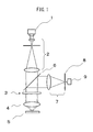
- FIG. 1 is a schematic configuration diagram of a laser microscope according to one embodiment of the invention.
- a light flux emitted from a laser light source 1 as a coherent light source is adjusted by a collimating optical system 2 into parallel light beam.
- the modulated light is focused on a specimen 5 through an objective lens 4.
- a light flux including specimen information such as a light flux reflected or scattered on the specimen 5 or fluorescent light generated on the specimen returns along an optical path, is reflected on a beam splitter 6, and is focused again on a confocal pinhole 8 by a confocal optical system 7 as a second optical system.
- the confocal pinhole 8 cuts a light flux on the specimen at a position other than the focus position. Therefore, it is possible to obtain a signal having a good S/N ratio by a detector 9.
- the objective lens 4 is designed taking into consideration parameters including not only the inside of a lens system, but also the refractive index and the length of the optical path from a lens tip to an observation plane, for instance, the thickness of a cover glass or the presence or absence of a cover glass, and in such a manner that the imaging performance of the objective lens is optimized under the condition with estimated values of these parameters.
- aberrations may be generated due to the depth of a biospecimen as an object to be observed, or a thickness deviation resulting from manufacturing error of a cover glass. The aberrations may lower the imaging performance.
- the laser microscope is configured to enhance the imaging performance by estimating wave front aberrations generated by an optical system from the laser light source 1 to the light focusing position of a light flux, including the objective lens 4, in accordance with the deviation of the optical path length from the design value; and by displaying, on the phase modulation device 3, a phase distribution that cancels the wave front aberrations as a phase modulation profile.
- phase modulation device 3 is disposed at a position conjugate to the pupil, with use of a relay lens. Further, a light flux emitted from the laser light source 1 passes through the phase modulation device 3 twice along an outward path and along a return path. Therefore, the phase modulation device 3 corrects the phase of the light flux along the outward path and along the return path.
- an objective lens in a microscope is designed to be an infinite system, and a light flux incident on the objective lens is a parallel light beam.
- phase modulation device 3 on the light source side of the objective lens 4, specifically, at a position in the vicinity of the objective lens 4. Disposing the phase modulation device 3 as described above is advantageous for the laser microscope to effectively obtain the correction effects.
- FIG. 2A and FIG. 2B are diagrams schematically illustrating aberrations generated depending on the depth of a specimen to be observed.
- the objective lens is designed to be optimized in observing a medium having a uniform refractive index.
- FIG. 2A illustrates a light flux 200 in observing a medium having a uniform refractive index, as used in the design.
- FIG. 2A illustrates that the light flux 200 is focused on one point without aberrations.
- FIG. 2B illustrates a light flux 210 in observing the surface of a specimen at the depth D.
- the light flux 210 is refracted on an interface 211 between the medium in contact with the objective lens and the specimen.
- the light flux 210 is not focused on one point due to the generated aberrations.
- the laser microscope is generates a phase distribution that cancels wave front aberrations, assuming that the generated aberrations are represented as the wave front aberrations at the pupil position of the objective lens 4, by applying voltages to electrodes of the phase modulation device 3 disposed at the pupil position of the objective lens.
- the laser microscope is operable to focus a light flux from the laser light source 1 on one point at an observation position defined on the surface of a specimen or in the inside of the specimen.
- a light flux generated on a specimen also returns along the optical path in the same manner as described above. Therefore, the laser microscope is operable to convert the light flux into a plane wave.
- Wave front aberrations can be represented as a sum of components by resolving the aberrations into the components. It is common to resolve wave front aberrations into orthogonal functions such as Zernike polynomials, and represent the wave front aberrations as a sum of the functions.
- a method for obtaining a correction amount for wave front aberrations by representing the correction amount as a phase distribution of each of the functions of Zernike polynomials, and by changing the relative phase modulation amount of each of the functions.
- the 13-th coefficient (Z 13 ) represents third-order spherical aberration
- 25-th coefficient (Z 25 ) represents fifth-order spherical aberration.
- Appropriately adjusting the phase distribution of a correction amount corresponding to each of the coefficients allows for the phase modulation device 3 to correct the third-order spherical aberration and the fifth-order spherical aberration.
- Aberrations generated in observing a deep part of a specimen are complex aberrations as combination of defocus or lower-order spherical aberrations and higher-order spherical aberrations. For instance, even if the phase modulation device 3 corrects Z 13 , improvement of the imaging performance is not sufficient. Further, Zernike polynomials are constituted of multitudes of terms. Therefore, it is necessary to create a phase modulation profile corresponding to each term, and to cause the phase modulation device 3 to display the phase modulation profiles in order to perform fine correction. In view of the above, it is preferable to dispose an element obtained by placing a plurality of aberration correction elements one over the other in a light flux, and to use at least one of the aberration correction elements so as to display the plurality of phase modulation profiles.
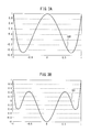
- FIG. 3A illustrates a curve 300 representing a phase distribution of third-order spherical aberration
- FIG. 3B illustrates a curve 301 representing a phase distribution of fifth-order spherical aberration.
- the aberrations in this case have a point-symmetric phase distribution.
- Each of the curves illustrates a sectional view of the phase distribution.
- the vertical axis indicates a value obtained by normalizing the phase difference, setting that the positive maximum value of the phase difference is "1”
- the horizontal axis indicates a value obtained by normalizing the effective diameter, setting that the maximum value of the effective diameter is "1”.
- the position "0" on the horizontal axis corresponds to a position on the optical axis.
- phase distribution of actually generated aberrations is a linear sum of these aberrations.
- a phase distribution is obtained by adding an adequate phase distribution component resulting from defocus to the phase distribution of a spherical aberration component which is the sum of a third-order spherical aberration component and a fifth-order spherical aberration component. Then, a profile, whose polarity is opposite to the polarity of the obtained phase distribution and which cancels the phase distribution, is defined as a phase modulation profile.
- the ratio between generated third-order spherical aberration and generated fifth-order spherical aberration is about 4:1, and it is possible to define a profile, whose polarity is opposite to the polarity of a phase distribution obtained by adding a phase component resulting from defocus to the linear sum of these spherical aberrations, as a phase modulation profile.
- phase modulation device 3 makes it possible to eliminate the repeating process for optimization, and to efficiently correct aberrations.
- the aberration components to be corrected by the phase modulation device 3 are not limited to defocus and spherical aberrations. It is possible to correct various generated aberrations, for instance, still higher-order aberrations, or aberrations that are not spherically symmetrical such as coma aberration. Each of the aberrations has an amount that enables to cancel the aberrations each other. Therefore, the total phase modulation amount in complex aberrations, which is the sum of aberrations of n kinds, is not equal to n-multiple of each of the aberration correction amounts.
- using the complex aberrations as aberrations to be corrected is advantageous because it is only necessary for the phase modulation device 3 to impart a light flux with a modulation amount sufficiently smaller than the total phase modulation amount in the complex aberrations.
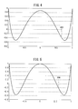
- phase modulation profile for use in actually correcting aberrations by the phase modulation device 3 is described in details by an example. It is conceived that a phase distribution that remains by focusing matches with a shape such that the root mean square (RMS) value of the wave front having the phase distribution is minimum. Therefore, for instance, there is proposed a method, in which a phase distribution of complex aberrations including a defocus term is obtained in such a manner that the RMS aberration is minimized, and a phase modulation profile is defined from the phase distribution.
- RMS root mean square
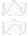
- a curve 400 illustrated in FIG. 4 represents a phase distribution of complex aberrations in which a defocus component and a spherical aberration generated on an objective lens whose numerical aperture NA is 1.0 are added in such a manner that the RMS aberration is minimized.
- phase modulation amount hereinafter, called as a PV value
- a phase distribution corresponding to the minimum phase modulation amount is defined as a phase modulation profile.
- a curve 500 illustrated in FIG. 5 represents a phase distribution of complex aberrations when a defocus component is added in such a manner that the PV value is minimized.
- the phase modulation range i.e. range of the phase modulation amount
- a response time of a liquid crystal element is proportional to a square of the thickness of a liquid crystal layer. Therefore, the smaller the phase modulation range is, the higher the response speed is. Further, the smaller the thickness of the liquid crystal layer is, the more the surface precision is.
- phase distribution that remains by focusing differs depending on the specifications of the microscope for use or the image processing software for use. It is possible to optimize the aberration correction by combining a residual aberration pattern specific to each of the microscope and the image processing software with the phase modulation profile of the phase modulation device.
- phase modulation device 3 configured such that a liquid crystal element is used as a phase modulation element, and a voltage is applied to each of electrodes of the liquid crystal element, while using a phase distribution that cancels wave front aberration as a phase modulation profile is described in detail, referring to FIGS. 6 to 9A , and 9B .
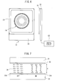
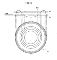
- FIG. 6 is a plan view of a phase modulation element 11 in the phase modulation device 3.
- a liquid crystal layer of the phase modulation element 11 is sandwiched between transparent substrates 21 and 22, and the periphery of the liquid crystal layer is sealed by a sealing member 23 so as to prevent leakage of liquid crystal.
- a plurality of transparent annular electrodes are formed in concentric form, the center of which is the optical axis, in an active region 24 that drives the liquid crystal, in other words, in a region capable of modulating the phase of a transmitting light flux, on surfaces of the transparent substrates 21 and 22 disposed to face each other.
- a transparent electrode may be formed on one of the transparent substrates 21 and 22 in such a manner as to cover the entirety of the active region 24.
- the active region 24 has a size determined in accordance with the pupil diameter of the objective lens. Controlling the voltages to be applied to the transparent annular electrodes by a control circuit 12 in the phase modulation device 3 makes it possible to impart a light flux transmitting through the phase modulation element 11 with an intended phase distribution.
- the control circuit 12 includes, for instance, a processor, and a drive circuit capable of changing the voltages to be output in accordance with a drive signal from the processor.
- FIG. 7 is a sectional schematic view of a part of the active region 24 of the phase modulation element 11 in FIG. 6 .
- the phase modulation element 11 is configured such that liquid crystal molecules 34 are sandwiched between the transparent substrates 21 and 22.
- Transparent electrodes 33, 33a, and 33b are formed on the surfaces of the transparent substrates 21 and 22 disposed to face each other.
- FIG. 7 illustrates a state that a voltage is applied between the electrode 33a on the right half side and the electrode 33, and a voltage is not applied between the electrode 33b on the left half side and the electrode 33.
- the liquid crystal molecules 34 have an elongated molecular structure, and are homogeneously aligned.
- the liquid crystal molecules 34 sandwiched between the two substrates 21 and 22 are aligned to be parallel to each other in the major axis direction thereof, and are aligned in parallel to each interface between each of the substrates 21 and 22 and the liquid crystal layer.
- the refractive index thereof in the major axis direction and the refractive index thereof in a direction orthogonal to the major axis direction differ from each other.
- the refractive index n e with respect to a polarized component (extraordinary ray) in parallel to the major axis direction of the liquid crystal molecules 34 is higher than the refractive index n o with respect to a polarized component (ordinary ray) in parallel to the minor axis direction of the liquid crystal molecules. Therefore, the phase modulation element 11 configured such that the liquid crystal molecules 34 are homogeneously aligned acts as a uniaxial birefringent element.
- Liquid crystal molecules have a dielectric anisotropy, and generally, a force is exerted on the liquid crystal molecules such that the major axis of the liquid crystal molecules is aligned with the electric field direction.
- a force is exerted on the liquid crystal molecules such that the major axis of the liquid crystal molecules is aligned with the electric field direction.
- the major axis direction of the liquid crystal molecules is inclined from a state in parallel to the substrates toward a direction orthogonal to the surfaces of the substrates in accordance with the voltage.
- the phase difference is 2 ⁇ nd/ ⁇ , where ⁇ is the wavelength of a light flux incident on the liquid crystal layer.
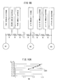
- FIG. 8 is a diagram illustrating a manner as to how a voltage application state is determined in accordance with a phase modulation profile.
- a curve 800 on the upper side in FIG. 8 represents a sectional view of a phase modulation profile corresponding to a plane passing the optical axis.
- annular electrodes 810 there are illustrated annular electrodes 810, for each of which an applied voltage value is determined in accordance with the phase modulation profile.
- the bold lines in FIG. 8 illustrate spaces between the annular electrodes.
- Lead-out electrodes and other elements are not illustrated to simplify the illustration.
- the annular electrodes corresponding to the position where the phase modulation amount is maximum and corresponding to the position where the phase modulation amount is minimum are determined from the phase modulation profile.
- the control circuit 12 applies an applied voltage serving as the maximum phase modulation amount, and an applied voltage serving as the minimum phase modulation amount to the corresponding annular electrodes, respectively.
- the annular electrodes adjacent to each other are connected by an electrode (a resistor) having a fixed electrical resistance. Therefore, the voltage difference between the annular electrodes adjacent to each other corresponds to a fixed step by resistance division. Further, controlling the applied voltages as described above is advantageous in simplifying the configuration of the control circuit 12, as compared with a circuit configured to control voltages to be applied to the annular electrodes independently of each other.
- FIGS. 9A and 9B are diagrams illustrating a relationship between annular electrodes and applied voltages to be applied thereto when the phase modulation device 3 has n annular electrodes.
- the center electrode is called as the first annular electrode
- the outermost peripheral annular electrode is called as the n-th annular electrode
- the annular electrode to which a maximum voltage is applied is called as the m-th annular electrode.
- FIG. 9A illustrates annular electrodes to which voltages are applied by the control circuit 12 by 2-level driving.
- a voltage V1 is applied to the first annular electrode at the center and to the n-th annular electrode at the outermost periphery, and a voltage V2 is applied to the m-th annular electrode.
- the voltage applied to the center electrode is made equal to the voltage value of the voltage to be applied to the n-th annular electrode at the outermost periphery. Further, applying the voltages as described above makes it possible to minimize the PV value. In this way, in the example of 2-level driving, it is possible to vary the amplitude of the phase modulation amount without changing the relative ratio of the phase modulation profile, with use of a difference between the applied voltages V1 and V2. Further, the above driving method has a feature that the phase modulation profile has a fixed shape, regardless of the advantage that the number of levels of the voltage values to be directly applied to the annular electrodes by the control circuit 12 are only two.
- FIG. 9B illustrates annular electrodes to which voltages are applied by the control circuit by 3-level driving.
- the method in FIG. 9B is substantially the same as the method for determining the voltage to be applied to each of the annular electrodes by 2-level driving in a point that the voltage to be applied to each of the annular electrodes is determined by resistance division.
- a voltage V3 to be applied to the n-th annular electrode at the outermost periphery by the control circuit 12 may be different from a voltage V1 to be applied to the first annular electrode.
- phase modulation device 3 uses the 3-level driving to display a phase modulation profile in accordance with objective lenses having a fixed pupil diameter but having numerical apertures NAs different from each other. Further, using the 3-level driving makes it possible to flexibly change the shape of a phase modulation profile such as approximation of a phase modulation profile to a profile corresponding to a different pupil diameter at a fixed numerical aperture NA. Thus, the phase modulation device 3 is operable to compensate aberrations, while suppressing residual aberrations.
- phase modulation device 3 Next, a method for varying a phase modulation profile to be displayed by the phase modulation device 3 in accordance with objective lenses having numerical apertures NAs different from each other is described in detail.
- FIG. 10A is a diagram illustrating a relationship between the numerical aperture NA and the ratio (Z 25 /Z 13 ) between Z 13 and Z 25 when the numerical aperture NA of the objective lens in the laser microscope is within the range of from 1.15 to 1.27, and the objective lens is an immersion lens.
- a straight line 1000 is an approximation straight line representing a relationship between the numerical aperture NA and the ratio (Z 25 /Z 13 ).
- FIG. 10B is a diagram illustrating a relationship between the numerical aperture NA and the ratio (Z 25 /Z 13 ) between Z 13 and Z 25 when the numerical aperture NA of the objective lens in the laser microscope is within the range of from 1.05 to 1.27.
- a straight line 1001 is an approximation straight line representing a relationship between the numerical aperture NA and the ratio (Z 25 /Z 13 ).
- FIG. 10C is a diagram illustrating a relationship between the numerical aperture NA and the ratio (Z 25 /Z 13 ) between Z 13 and Z 25 when the numerical aperture NA of the objective lens in the laser microscope is within the range of from 0.75 to 0.95, and the objective lens is a dry lens.
- a straight line 1002 is an approximation straight line representing a relationship between the numerical aperture NA and the ratio (Z 25 /Z 13 ).
- the horizontal axis indicates the numerical aperture NA
- the vertical axis indicates the ratio (Z 25 /Z 13 ).
- the curves 1000 to 1002 are respectively represented by the following equations (1) to (3).
- Z 25 Z 13 1.91 ⁇ NA - 1.87
- Z 25 Z 13 1.37 ⁇ NA - 1.21
- Z 25 Z 13 1.06 ⁇ NA - 0.64
- the phase distribution to compensate the generated spherical aberrations may be a linear sum of aberrations represented by the ratios as described above.
- a Strehl ratio as one of the indexes indicating the performance of an optical imaging system is known.
- the Strehl ratio is a ratio between a peak luminance, on an imaging surface, of light from a point light source in an optical system, and a peak luminance in a diffraction limit optical system.
- An optical system having a Strehl ratio closer to 1 is regarded as an optical system having a higher imaging performance.
- the Strehl ratio is 0.8 or larger, it is possible to neglect the influence on the imaging performance due to residual aberrations (see e.g. page 198 "Introduction to Optics for User Engineers" by Toshiro KISHIKAWA, published by the Optronics Co., Ltd.).
- the Strehl ratio and the wave front aberration have a relationship as represented by the equation (4). Further, the relationship between the wave front aberration (RMS value) and each of the wave front aberration coefficients is represented by the equation (5).
- third-order spherical aberration A 13 is generated in an immersion objective lens whose numerical aperture NA is 1.2, for instance, it is conceived that fifth-order spherical aberration is generated by 0.45A 13 .
- (x ⁇ A 13 )/(7 1/2 ) (RMS value) remains as fifth-order aberration according to the equation (5).
- the ratio (A 25 /A 13 ) may satisfy the relationship represented by the following equation.
- Third-order spherical aberration coefficient of spherical aberration generated by the presence or absence of a cover glass is about 5.2, taking into consideration that the thickness of a general cover glass is 0.17 mm. It is preferable for the phase modulation device 3 to correct the aforementioned aberrations from a neutral position. Therefore, a correction amount having a range of about 10 is necessary.
- the value of x is a little less than 0.23 when the wavelength is 488 nm, for instance, according to the equation (6) described above.
- the ratio of fifth-order spherical aberration with respect to third-order spherical aberration is preferably about 0.42 ⁇ 0.23.
- phase modulation profile in accordance with a variety of combinations of pupil diameters and numerical apertures NAs.
- the control circuit 12 is operable to apply an intended voltage to each of the annular electrodes.
- the control circuit 12 is operable to cause the phase modulation element 11 to display a phase modulation profile in accordance with the pupil diameter and the numerical aperture NA by controlling the voltages to be applied to the annular electrodes independently of each other.
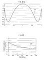
- FIGS. 11A, 11B , and 11C illustrate a difference in phase distribution of aberration due to a difference in numeral aperture NA of the objective lens.
- a curve 1100 illustrated in FIG. 11A , a curve 1101 illustrated in FIG. 11B , and a curve 1102 illustrated in FIG. 11C respectively indicate phase distributions of complex aberrations when the numerical aperture NA is 1.0, 1.2, and 0.8.
- the vertical axis indicates a value obtained by normalizing the phase difference, setting that the positive maximum value of the phase difference is "1”
- the horizontal axis indicates a value obtained by normalizing the effective diameter, setting that the maximum value of the effective diameter is "1".
- the defocus value is fixed with respect to each of the numerical apertures NAs.
- the control circuit 12 controls the voltage to be applied to each of the annular electrodes by 3-level driving as illustrated in FIG. 9B so that various phase modulation profiles are reproducible.
- the ratios between the voltages V1, V2, and V3 to be applied to the first annular electrode, the m-th annular electrode, and the n-th annular electrode are obtained in advance in such a manner that the phase distribution of aberration is cancelled, each time the objective lens is exchanged.
- a storage unit in the control circuit 12 may store in advance the ratios between the voltages in correspondence to the pupil diameter and the numerical aperture NA of the objective lens.
- the control circuit 12 may read the ratios between the voltages V1, V2, and V3 in accordance with the objective lens from the storage unit, and may determine the voltage to be applied to each of the annular electrodes in accordance with the ratios.
- the final voltage adjustment (voltages V1, V2, and V3) may be manually performed by allowing the user to view an image via an unillustrated user interface.
- the control circuit 12 may automatically set the voltages that maximize the contrast, while feedback controlling the information to be obtained from an image such as contrast.
- a phase difference depends on the wavelength of light to be incident on a liquid crystal layer.
- the laser light source 1 in a general laser microscope is operable to irradiate laser light of a selected wavelength from among a plurality of wavelengths of laser light.
- a required phase modulation amount differs depending on the wavelength of laser light for use. Therefore, it is necessary for the control circuit 12 of the phase modulation device 3 to correct the phase modulation amount due to the phase modulation element 11.
- the control circuit is operable to correct a phase modulation amount deviation due to a difference in wavelength by changing the voltage to be applied to the liquid crystal layer of the phase modulation device 3.
- the control circuit 12 is operable to cancel a phase modulation amount deviation due to a temperature difference or the like by adjusting the voltage to be applied to the liquid crystal layer of the phase modulation element 11.
- a curve 1200 illustrated in FIG. 12 indicates wavelength dispersion characteristics of liquid crystal provided and sealed in a liquid crystal layer of the phase modulation device 3 in the foregoing embodiment.
- the horizontal axis indicates a wavelength
- the vertical axis indicates a value obtained by normalizing the phase difference ( ⁇ nd) of the phase modulation device 3 in such a manner that the value of the phase difference when the wavelength is 550 nm is equal to 1.
- the degree of wavelength dispersion is 1.057 when the wavelength of laser light is 488 nm, and the degree of wavelength dispersion is 1.200 when the wavelength of laser light is 405 nm.
- phase modulation profile by adding a degree of wavelength dispersion optimum for a target wavelength, as a parameter, to the calculation equation representing a phase modulation profile so that the phase modulation element 11 imparts a transmitting light flux with the optimum phase modulation profile.
- the wavelength of the laser light source 1 for use as a parameter in order to create a phase modulation profile.
- multiplying a degree of wavelength dispersion as illustrated in FIG. 12 as a coefficient by the phase modulation profile created as described above makes it possible to obtain an optimized phase modulation profile, taking into consideration of the wavelength of laser light from the laser light source.
- the control circuit 12 may adjust the voltage to be applied to each of the electrodes of the phase modulation element 11, based on the optimized phase modulation profile.
- a liquid crystal element is used as the phase modulation element of the phase modulation device, but the phase modulation element is not limited to a liquid crystal element.
- an optical crystal element having an electro-optical effect as represented by a Pockels effect may be used as the phase modulation element.
- annular electrodes the center of which is the optical axis are mounted on one surface of an optical crystal element on a flat plate, and an electrode is mounted on the other surface of the optical crystal element so as to cover the entirety of the surface.
- each of the electrodes may preferably be a transparent electrode.
- adjusting the voltage applied to each of the annular electrodes by the control circuit makes it possible to cause the optical crystal element to display a phase modulation profile for correcting aberrations of an optical system including an objective lens, and to impart a light flux transmitting through the optical crystal element with a phase distribution in accordance with the phase modulation profile.
- a deformable mirror may be used as the phase modulation element, although the deformable mirror is of a reflective-type mirror.
- annular electrodes the center of which is the optical axis, are mounted on the deformable mirror. Adjusting the voltage to be applied to each of the annular electrodes by the control circuit makes it possible to represent a phase modulation profile that corrects aberrations of an optical system including an objective lens by the deformable mirror, and to impart a light flux reflected on the deformable mirror with a phase distribution in accordance with the phase modulation profile.
- phase modulation device of the invention is not limited to the above example.
- the invention may be applied to any optical apparatus, as far as the optical apparatus is provided with an objective lens and is incorporated with a coherent light source.
- the invention is also applicable to an OCT (Optical Coherence Tomography), for instance.
Landscapes
- Physics & Mathematics (AREA)
- General Physics & Mathematics (AREA)
- Optics & Photonics (AREA)
- Chemical & Material Sciences (AREA)
- Analytical Chemistry (AREA)
- Microscoopes, Condenser (AREA)
- Liquid Crystal (AREA)
- Optical Modulation, Optical Deflection, Nonlinear Optics, Optical Demodulation, Optical Logic Elements (AREA)
- Optical Head (AREA)
Applications Claiming Priority (3)
| Application Number | Priority Date | Filing Date | Title |
|---|---|---|---|
| JP2012021665 | 2012-02-03 | ||
| JP2012150194 | 2012-07-04 | ||
| PCT/JP2013/052390 WO2013115383A1 (ja) | 2012-02-03 | 2013-02-01 | 位相変調デバイス及びレーザ顕微鏡 |
Publications (3)
| Publication Number | Publication Date |
|---|---|
| EP2811335A1 true EP2811335A1 (de) | 2014-12-10 |
| EP2811335A4 EP2811335A4 (de) | 2015-09-02 |
| EP2811335B1 EP2811335B1 (de) | 2019-10-30 |
Family
ID=48905410
Family Applications (1)
| Application Number | Title | Priority Date | Filing Date |
|---|---|---|---|
| EP13743360.3A Active EP2811335B1 (de) | 2012-02-03 | 2013-02-01 | Phasenmodulationsvorrichtung und lasermikroskop |
Country Status (5)
| Country | Link |
|---|---|
| US (1) | US9383573B2 (de) |
| EP (1) | EP2811335B1 (de) |
| JP (1) | JP6157364B2 (de) |
| CN (1) | CN104081259B (de) |
| WO (1) | WO2013115383A1 (de) |
Families Citing this family (18)
| Publication number | Priority date | Publication date | Assignee | Title |
|---|---|---|---|---|
| CN104303090B (zh) * | 2012-05-17 | 2017-08-15 | 西铁城时计株式会社 | 像差校正器件及激光显微镜 |
| JP6355928B2 (ja) * | 2014-01-27 | 2018-07-11 | オリンパス株式会社 | 蛍光観察装置 |
| JP6378931B2 (ja) * | 2014-05-21 | 2018-08-22 | 浜松ホトニクス株式会社 | 顕微鏡装置及び画像取得方法 |
| DE102014110208B4 (de) * | 2014-07-21 | 2022-05-25 | Leica Microsystems Cms Gmbh | Abtastmikroskop |
| JP6462705B2 (ja) * | 2014-09-25 | 2019-01-30 | シチズン時計株式会社 | 位相変調デバイス及びレーザ顕微鏡 |
| US10112262B2 (en) * | 2014-10-28 | 2018-10-30 | General Electric Company | System and methods for real-time enhancement of build parameters of a component |
| US10295838B1 (en) * | 2015-09-30 | 2019-05-21 | Apple Inc. | Body including surface having concentric annular portions |
| JP6634263B2 (ja) | 2015-10-16 | 2020-01-22 | オリンパス株式会社 | 顕微鏡 |
| US20180045960A1 (en) | 2015-12-02 | 2018-02-15 | Augmenteum, LLC. | System for and method of projecting augmentation imagery in a head-mounted display |
| JP6577890B2 (ja) * | 2016-03-17 | 2019-09-18 | シチズン時計株式会社 | 光学装置 |
| DE102017105928B4 (de) * | 2017-03-20 | 2024-08-14 | Carl Zeiss Microscopy Gmbh | Mikroskop und Verfahren zum Abbilden eines Objektes |
| JP6539391B2 (ja) * | 2018-07-30 | 2019-07-03 | 浜松ホトニクス株式会社 | 顕微鏡装置及び画像取得方法 |
| DE102019008304B8 (de) | 2019-11-29 | 2021-06-02 | Abberior Instruments Gmbh | Fluoreszenzmikroskop mit stabilisierter Justage und Verwendung einer Baugruppe zur Aufrüstung eines Fluoreszenzmikroskops |
| JP7564719B2 (ja) * | 2021-01-28 | 2024-10-09 | 浜松ホトニクス株式会社 | レーザ加工装置及びレーザ加工方法 |
| US12393765B2 (en) | 2021-08-06 | 2025-08-19 | Samsung Electronics Co., Ltd. | Automating search for improved display structure for under-display camera systems |
| US12216277B2 (en) * | 2021-10-14 | 2025-02-04 | Samsung Electronics Co., Ltd. | Optical element for deconvolution |
| US12482075B2 (en) | 2022-06-08 | 2025-11-25 | Samsung Electronics Co., Ltd. | Restoring images using deconvolution |
| CN117420098B (zh) * | 2023-10-09 | 2024-08-02 | 西安电子科技大学 | 一种自适应衍射相位显微成像装置及方法 |
Family Cites Families (16)
| Publication number | Priority date | Publication date | Assignee | Title |
|---|---|---|---|---|
| JP3299808B2 (ja) | 1993-03-29 | 2002-07-08 | オリンパス光学工業株式会社 | 液浸系顕微鏡対物レンズ |
| JP3819213B2 (ja) * | 2000-04-14 | 2006-09-06 | 三星電機株式会社 | 光ピックアップ |
| US7209426B2 (en) * | 2002-11-08 | 2007-04-24 | Citizen Watch Co., Ltd. | Liquid crystal optical element and optical device |
| JP2004239660A (ja) * | 2003-02-04 | 2004-08-26 | Japan Science & Technology Agency | 顕微鏡 |
| JP2004247947A (ja) * | 2003-02-13 | 2004-09-02 | Olympus Corp | 光学装置 |
| JP4149309B2 (ja) | 2003-05-19 | 2008-09-10 | オリンパス株式会社 | 走査型光学顕微鏡 |
| US6906866B2 (en) * | 2003-10-15 | 2005-06-14 | Carl Zeiss Smt Ag | Compact 1½-waist system for sub 100 nm ArF lithography |
| JP4509591B2 (ja) * | 2004-02-10 | 2010-07-21 | 株式会社トプコン | 収差補正機能付き画像形成装置 |
| JP2005267756A (ja) | 2004-03-18 | 2005-09-29 | Sharp Corp | 位相補正素子、それを用いた光ピックアップ装置及び情報記録再生装置 |
| JP4709582B2 (ja) | 2005-05-23 | 2011-06-22 | シチズンホールディングス株式会社 | 液晶光学素子、光学装置及び開口制御方法 |
| JP4581969B2 (ja) | 2005-11-14 | 2010-11-17 | コニカミノルタホールディングス株式会社 | 液晶デバイスおよび光ピックアップ |
| JP4776450B2 (ja) * | 2006-06-16 | 2011-09-21 | 株式会社トプコン | 眼科撮影装置 |
| JP5692969B2 (ja) * | 2008-09-01 | 2015-04-01 | 浜松ホトニクス株式会社 | 収差補正方法、この収差補正方法を用いたレーザ加工方法、この収差補正方法を用いたレーザ照射方法、収差補正装置、及び、収差補正プログラム |
| GB0907277D0 (en) * | 2009-04-29 | 2009-06-10 | Univ Kent Kanterbury | Method for depth resolved wavefront sensing, depth resolved wavefront sensors and method and apparatus for optical imaging |
| US8559014B2 (en) * | 2009-09-25 | 2013-10-15 | Hwan J. Jeong | High-resolution, common-path interferometric imaging systems and methods |
| JP5693559B2 (ja) | 2010-02-26 | 2015-04-01 | 独立行政法人科学技術振興機構 | 顕微鏡装置、光ピックアップ装置及び光照射装置 |
-
2013
- 2013-02-01 EP EP13743360.3A patent/EP2811335B1/de active Active
- 2013-02-01 CN CN201380007865.4A patent/CN104081259B/zh not_active Expired - Fee Related
- 2013-02-01 WO PCT/JP2013/052390 patent/WO2013115383A1/ja not_active Ceased
- 2013-02-01 US US14/376,423 patent/US9383573B2/en not_active Expired - Fee Related
- 2013-02-01 JP JP2013556524A patent/JP6157364B2/ja not_active Expired - Fee Related
Also Published As
| Publication number | Publication date |
|---|---|
| CN104081259B (zh) | 2017-06-06 |
| JPWO2013115383A1 (ja) | 2015-05-11 |
| US20150338639A1 (en) | 2015-11-26 |
| CN104081259A (zh) | 2014-10-01 |
| JP6157364B2 (ja) | 2017-07-05 |
| US9383573B2 (en) | 2016-07-05 |
| EP2811335B1 (de) | 2019-10-30 |
| WO2013115383A1 (ja) | 2013-08-08 |
| EP2811335A4 (de) | 2015-09-02 |
Similar Documents
| Publication | Publication Date | Title |
|---|---|---|
| US9383573B2 (en) | Phase modulation device and laser microscope | |
| US9594238B2 (en) | Aberration correction device and laser microscope | |
| CN104583845B (zh) | 像差校正光学单元及激光显微镜 | |
| KR102900996B1 (ko) | 재료들 내부에서의 레이저 가공 | |
| US11685003B2 (en) | Method for laser machining inside materials | |
| US9979586B2 (en) | Phase modulation device and laser microscope | |
| JP6850684B2 (ja) | 光計測装置 | |
| Tao et al. | Shack-Hartmann wavefront sensing using interferometric focusing of light onto guide-stars | |
| Le Moal et al. | Isotropic single-objective microscopy: theory and experiment | |
| JP6577890B2 (ja) | 光学装置 |
Legal Events
| Date | Code | Title | Description |
|---|---|---|---|
| PUAI | Public reference made under article 153(3) epc to a published international application that has entered the european phase |
Free format text: ORIGINAL CODE: 0009012 |
|
| 17P | Request for examination filed |
Effective date: 20140731 |
|
| AK | Designated contracting states |
Kind code of ref document: A1 Designated state(s): AL AT BE BG CH CY CZ DE DK EE ES FI FR GB GR HR HU IE IS IT LI LT LU LV MC MK MT NL NO PL PT RO RS SE SI SK SM TR |
|
| AX | Request for extension of the european patent |
Extension state: BA ME |
|
| DAX | Request for extension of the european patent (deleted) | ||
| RA4 | Supplementary search report drawn up and despatched (corrected) |
Effective date: 20150805 |
|
| RIC1 | Information provided on ipc code assigned before grant |
Ipc: G02B 21/00 20060101ALI20150730BHEP Ipc: G02B 26/06 20060101ALI20150730BHEP Ipc: G02F 1/01 20060101AFI20150730BHEP Ipc: G02B 21/08 20060101ALI20150730BHEP Ipc: G02F 1/13 20060101ALI20150730BHEP Ipc: G02B 3/14 20060101ALI20150730BHEP Ipc: G02F 1/1343 20060101ALN20150730BHEP |
|
| RAP1 | Party data changed (applicant data changed or rights of an application transferred) |
Owner name: CITIZEN WATCH CO., LTD. |
|
| STAA | Information on the status of an ep patent application or granted ep patent |
Free format text: STATUS: EXAMINATION IS IN PROGRESS |
|
| 17Q | First examination report despatched |
Effective date: 20180720 |
|
| GRAP | Despatch of communication of intention to grant a patent |
Free format text: ORIGINAL CODE: EPIDOSNIGR1 |
|
| STAA | Information on the status of an ep patent application or granted ep patent |
Free format text: STATUS: GRANT OF PATENT IS INTENDED |
|
| RIC1 | Information provided on ipc code assigned before grant |
Ipc: G02B 26/06 20060101ALI20190502BHEP Ipc: G02F 1/13 20060101ALI20190502BHEP Ipc: G02B 3/14 20060101ALI20190502BHEP Ipc: G02B 21/00 20060101ALI20190502BHEP Ipc: G02F 1/1343 20060101ALN20190502BHEP Ipc: G02B 21/08 20060101ALI20190502BHEP Ipc: G02F 1/01 20060101AFI20190502BHEP |
|
| INTG | Intention to grant announced |
Effective date: 20190528 |
|
| GRAS | Grant fee paid |
Free format text: ORIGINAL CODE: EPIDOSNIGR3 |
|
| GRAA | (expected) grant |
Free format text: ORIGINAL CODE: 0009210 |
|
| STAA | Information on the status of an ep patent application or granted ep patent |
Free format text: STATUS: THE PATENT HAS BEEN GRANTED |
|
| AK | Designated contracting states |
Kind code of ref document: B1 Designated state(s): AL AT BE BG CH CY CZ DE DK EE ES FI FR GB GR HR HU IE IS IT LI LT LU LV MC MK MT NL NO PL PT RO RS SE SI SK SM TR |
|
| REG | Reference to a national code |
Ref country code: GB Ref legal event code: FG4D |
|
| REG | Reference to a national code |
Ref country code: CH Ref legal event code: EP |
|
| REG | Reference to a national code |
Ref country code: AT Ref legal event code: REF Ref document number: 1196780 Country of ref document: AT Kind code of ref document: T Effective date: 20191115 |
|
| REG | Reference to a national code |
Ref country code: DE Ref legal event code: R096 Ref document number: 602013062247 Country of ref document: DE |
|
| REG | Reference to a national code |
Ref country code: IE Ref legal event code: FG4D |
|
| REG | Reference to a national code |
Ref country code: CH Ref legal event code: NV Representative=s name: PATENTANWAELTE SCHAAD, BALASS, MENZL AND PARTN, CH |
|
| REG | Reference to a national code |
Ref country code: LT Ref legal event code: MG4D |
|
| PG25 | Lapsed in a contracting state [announced via postgrant information from national office to epo] |
Ref country code: FI Free format text: LAPSE BECAUSE OF FAILURE TO SUBMIT A TRANSLATION OF THE DESCRIPTION OR TO PAY THE FEE WITHIN THE PRESCRIBED TIME-LIMIT Effective date: 20191030 Ref country code: BG Free format text: LAPSE BECAUSE OF FAILURE TO SUBMIT A TRANSLATION OF THE DESCRIPTION OR TO PAY THE FEE WITHIN THE PRESCRIBED TIME-LIMIT Effective date: 20200130 Ref country code: LT Free format text: LAPSE BECAUSE OF FAILURE TO SUBMIT A TRANSLATION OF THE DESCRIPTION OR TO PAY THE FEE WITHIN THE PRESCRIBED TIME-LIMIT Effective date: 20191030 Ref country code: PT Free format text: LAPSE BECAUSE OF FAILURE TO SUBMIT A TRANSLATION OF THE DESCRIPTION OR TO PAY THE FEE WITHIN THE PRESCRIBED TIME-LIMIT Effective date: 20200302 Ref country code: ES Free format text: LAPSE BECAUSE OF FAILURE TO SUBMIT A TRANSLATION OF THE DESCRIPTION OR TO PAY THE FEE WITHIN THE PRESCRIBED TIME-LIMIT Effective date: 20191030 Ref country code: LV Free format text: LAPSE BECAUSE OF FAILURE TO SUBMIT A TRANSLATION OF THE DESCRIPTION OR TO PAY THE FEE WITHIN THE PRESCRIBED TIME-LIMIT Effective date: 20191030 Ref country code: SE Free format text: LAPSE BECAUSE OF FAILURE TO SUBMIT A TRANSLATION OF THE DESCRIPTION OR TO PAY THE FEE WITHIN THE PRESCRIBED TIME-LIMIT Effective date: 20191030 Ref country code: NL Free format text: LAPSE BECAUSE OF FAILURE TO SUBMIT A TRANSLATION OF THE DESCRIPTION OR TO PAY THE FEE WITHIN THE PRESCRIBED TIME-LIMIT Effective date: 20191030 Ref country code: PL Free format text: LAPSE BECAUSE OF FAILURE TO SUBMIT A TRANSLATION OF THE DESCRIPTION OR TO PAY THE FEE WITHIN THE PRESCRIBED TIME-LIMIT Effective date: 20191030 Ref country code: GR Free format text: LAPSE BECAUSE OF FAILURE TO SUBMIT A TRANSLATION OF THE DESCRIPTION OR TO PAY THE FEE WITHIN THE PRESCRIBED TIME-LIMIT Effective date: 20200131 Ref country code: NO Free format text: LAPSE BECAUSE OF FAILURE TO SUBMIT A TRANSLATION OF THE DESCRIPTION OR TO PAY THE FEE WITHIN THE PRESCRIBED TIME-LIMIT Effective date: 20200130 |
|
| PGFP | Annual fee paid to national office [announced via postgrant information from national office to epo] |
Ref country code: DE Payment date: 20200220 Year of fee payment: 8 |
|
| REG | Reference to a national code |
Ref country code: NL Ref legal event code: MP Effective date: 20191030 |
|
| PG25 | Lapsed in a contracting state [announced via postgrant information from national office to epo] |
Ref country code: IS Free format text: LAPSE BECAUSE OF FAILURE TO SUBMIT A TRANSLATION OF THE DESCRIPTION OR TO PAY THE FEE WITHIN THE PRESCRIBED TIME-LIMIT Effective date: 20200229 Ref country code: HR Free format text: LAPSE BECAUSE OF FAILURE TO SUBMIT A TRANSLATION OF THE DESCRIPTION OR TO PAY THE FEE WITHIN THE PRESCRIBED TIME-LIMIT Effective date: 20191030 Ref country code: RS Free format text: LAPSE BECAUSE OF FAILURE TO SUBMIT A TRANSLATION OF THE DESCRIPTION OR TO PAY THE FEE WITHIN THE PRESCRIBED TIME-LIMIT Effective date: 20191030 |
|
| PGFP | Annual fee paid to national office [announced via postgrant information from national office to epo] |
Ref country code: CH Payment date: 20200204 Year of fee payment: 8 |
|
| PG25 | Lapsed in a contracting state [announced via postgrant information from national office to epo] |
Ref country code: AL Free format text: LAPSE BECAUSE OF FAILURE TO SUBMIT A TRANSLATION OF THE DESCRIPTION OR TO PAY THE FEE WITHIN THE PRESCRIBED TIME-LIMIT Effective date: 20191030 |
|
| PG25 | Lapsed in a contracting state [announced via postgrant information from national office to epo] |
Ref country code: RO Free format text: LAPSE BECAUSE OF FAILURE TO SUBMIT A TRANSLATION OF THE DESCRIPTION OR TO PAY THE FEE WITHIN THE PRESCRIBED TIME-LIMIT Effective date: 20191030 Ref country code: CZ Free format text: LAPSE BECAUSE OF FAILURE TO SUBMIT A TRANSLATION OF THE DESCRIPTION OR TO PAY THE FEE WITHIN THE PRESCRIBED TIME-LIMIT Effective date: 20191030 Ref country code: EE Free format text: LAPSE BECAUSE OF FAILURE TO SUBMIT A TRANSLATION OF THE DESCRIPTION OR TO PAY THE FEE WITHIN THE PRESCRIBED TIME-LIMIT Effective date: 20191030 Ref country code: DK Free format text: LAPSE BECAUSE OF FAILURE TO SUBMIT A TRANSLATION OF THE DESCRIPTION OR TO PAY THE FEE WITHIN THE PRESCRIBED TIME-LIMIT Effective date: 20191030 |
|
| REG | Reference to a national code |
Ref country code: DE Ref legal event code: R097 Ref document number: 602013062247 Country of ref document: DE |
|
| REG | Reference to a national code |
Ref country code: AT Ref legal event code: MK05 Ref document number: 1196780 Country of ref document: AT Kind code of ref document: T Effective date: 20191030 |
|
| PG25 | Lapsed in a contracting state [announced via postgrant information from national office to epo] |
Ref country code: SK Free format text: LAPSE BECAUSE OF FAILURE TO SUBMIT A TRANSLATION OF THE DESCRIPTION OR TO PAY THE FEE WITHIN THE PRESCRIBED TIME-LIMIT Effective date: 20191030 Ref country code: IT Free format text: LAPSE BECAUSE OF FAILURE TO SUBMIT A TRANSLATION OF THE DESCRIPTION OR TO PAY THE FEE WITHIN THE PRESCRIBED TIME-LIMIT Effective date: 20191030 Ref country code: SM Free format text: LAPSE BECAUSE OF FAILURE TO SUBMIT A TRANSLATION OF THE DESCRIPTION OR TO PAY THE FEE WITHIN THE PRESCRIBED TIME-LIMIT Effective date: 20191030 |
|
| PLBE | No opposition filed within time limit |
Free format text: ORIGINAL CODE: 0009261 |
|
| STAA | Information on the status of an ep patent application or granted ep patent |
Free format text: STATUS: NO OPPOSITION FILED WITHIN TIME LIMIT |
|
| 26N | No opposition filed |
Effective date: 20200731 |
|
| GBPC | Gb: european patent ceased through non-payment of renewal fee |
Effective date: 20200201 |
|
| REG | Reference to a national code |
Ref country code: BE Ref legal event code: MM Effective date: 20200229 |
|
| PG25 | Lapsed in a contracting state [announced via postgrant information from national office to epo] |
Ref country code: LU Free format text: LAPSE BECAUSE OF NON-PAYMENT OF DUE FEES Effective date: 20200201 Ref country code: MC Free format text: LAPSE BECAUSE OF FAILURE TO SUBMIT A TRANSLATION OF THE DESCRIPTION OR TO PAY THE FEE WITHIN THE PRESCRIBED TIME-LIMIT Effective date: 20191030 |
|
| PG25 | Lapsed in a contracting state [announced via postgrant information from national office to epo] |
Ref country code: AT Free format text: LAPSE BECAUSE OF FAILURE TO SUBMIT A TRANSLATION OF THE DESCRIPTION OR TO PAY THE FEE WITHIN THE PRESCRIBED TIME-LIMIT Effective date: 20191030 Ref country code: SI Free format text: LAPSE BECAUSE OF FAILURE TO SUBMIT A TRANSLATION OF THE DESCRIPTION OR TO PAY THE FEE WITHIN THE PRESCRIBED TIME-LIMIT Effective date: 20191030 |
|
| PG25 | Lapsed in a contracting state [announced via postgrant information from national office to epo] |
Ref country code: FR Free format text: LAPSE BECAUSE OF NON-PAYMENT OF DUE FEES Effective date: 20200229 Ref country code: GB Free format text: LAPSE BECAUSE OF NON-PAYMENT OF DUE FEES Effective date: 20200201 Ref country code: IE Free format text: LAPSE BECAUSE OF NON-PAYMENT OF DUE FEES Effective date: 20200201 |
|
| PG25 | Lapsed in a contracting state [announced via postgrant information from national office to epo] |
Ref country code: BE Free format text: LAPSE BECAUSE OF NON-PAYMENT OF DUE FEES Effective date: 20200229 |
|
| REG | Reference to a national code |
Ref country code: DE Ref legal event code: R119 Ref document number: 602013062247 Country of ref document: DE |
|
| PG25 | Lapsed in a contracting state [announced via postgrant information from national office to epo] |
Ref country code: LI Free format text: LAPSE BECAUSE OF NON-PAYMENT OF DUE FEES Effective date: 20210228 Ref country code: CH Free format text: LAPSE BECAUSE OF NON-PAYMENT OF DUE FEES Effective date: 20210228 |
|
| PG25 | Lapsed in a contracting state [announced via postgrant information from national office to epo] |
Ref country code: DE Free format text: LAPSE BECAUSE OF NON-PAYMENT OF DUE FEES Effective date: 20210901 |
|
| PG25 | Lapsed in a contracting state [announced via postgrant information from national office to epo] |
Ref country code: TR Free format text: LAPSE BECAUSE OF FAILURE TO SUBMIT A TRANSLATION OF THE DESCRIPTION OR TO PAY THE FEE WITHIN THE PRESCRIBED TIME-LIMIT Effective date: 20191030 Ref country code: MT Free format text: LAPSE BECAUSE OF FAILURE TO SUBMIT A TRANSLATION OF THE DESCRIPTION OR TO PAY THE FEE WITHIN THE PRESCRIBED TIME-LIMIT Effective date: 20191030 Ref country code: CY Free format text: LAPSE BECAUSE OF FAILURE TO SUBMIT A TRANSLATION OF THE DESCRIPTION OR TO PAY THE FEE WITHIN THE PRESCRIBED TIME-LIMIT Effective date: 20191030 |
|
| PG25 | Lapsed in a contracting state [announced via postgrant information from national office to epo] |
Ref country code: MK Free format text: LAPSE BECAUSE OF FAILURE TO SUBMIT A TRANSLATION OF THE DESCRIPTION OR TO PAY THE FEE WITHIN THE PRESCRIBED TIME-LIMIT Effective date: 20191030 |