EP2805243B1 - Hybrid write-through/write-back cache policy managers, and related systems and methods - Google Patents
Hybrid write-through/write-back cache policy managers, and related systems and methods Download PDFInfo
- Publication number
- EP2805243B1 EP2805243B1 EP13701347.0A EP13701347A EP2805243B1 EP 2805243 B1 EP2805243 B1 EP 2805243B1 EP 13701347 A EP13701347 A EP 13701347A EP 2805243 B1 EP2805243 B1 EP 2805243B1
- Authority
- EP
- European Patent Office
- Prior art keywords
- cache
- caches
- write
- active
- parallel
- Prior art date
- Legal status (The legal status is an assumption and is not a legal conclusion. Google has not performed a legal analysis and makes no representation as to the accuracy of the status listed.)
- Not-in-force
Links
Images


Classifications
-
- G—PHYSICS
- G06—COMPUTING; CALCULATING OR COUNTING
- G06F—ELECTRIC DIGITAL DATA PROCESSING
- G06F12/00—Accessing, addressing or allocating within memory systems or architectures
- G06F12/02—Addressing or allocation; Relocation
- G06F12/08—Addressing or allocation; Relocation in hierarchically structured memory systems, e.g. virtual memory systems
- G06F12/0802—Addressing of a memory level in which the access to the desired data or data block requires associative addressing means, e.g. caches
- G06F12/0804—Addressing of a memory level in which the access to the desired data or data block requires associative addressing means, e.g. caches with main memory updating
-
- G—PHYSICS
- G06—COMPUTING; CALCULATING OR COUNTING
- G06F—ELECTRIC DIGITAL DATA PROCESSING
- G06F1/00—Details not covered by groups G06F3/00 - G06F13/00 and G06F21/00
- G06F1/26—Power supply means, e.g. regulation thereof
- G06F1/32—Means for saving power
-
- G—PHYSICS
- G06—COMPUTING; CALCULATING OR COUNTING
- G06F—ELECTRIC DIGITAL DATA PROCESSING
- G06F1/00—Details not covered by groups G06F3/00 - G06F13/00 and G06F21/00
- G06F1/26—Power supply means, e.g. regulation thereof
- G06F1/32—Means for saving power
- G06F1/3203—Power management, i.e. event-based initiation of a power-saving mode
- G06F1/3234—Power saving characterised by the action undertaken
- G06F1/325—Power saving in peripheral device
- G06F1/3275—Power saving in memory, e.g. RAM, cache
-
- G—PHYSICS
- G06—COMPUTING; CALCULATING OR COUNTING
- G06F—ELECTRIC DIGITAL DATA PROCESSING
- G06F1/00—Details not covered by groups G06F3/00 - G06F13/00 and G06F21/00
- G06F1/26—Power supply means, e.g. regulation thereof
- G06F1/32—Means for saving power
- G06F1/3203—Power management, i.e. event-based initiation of a power-saving mode
- G06F1/3234—Power saving characterised by the action undertaken
- G06F1/3287—Power saving characterised by the action undertaken by switching off individual functional units in the computer system
-
- G—PHYSICS
- G06—COMPUTING; CALCULATING OR COUNTING
- G06F—ELECTRIC DIGITAL DATA PROCESSING
- G06F12/00—Accessing, addressing or allocating within memory systems or architectures
- G06F12/02—Addressing or allocation; Relocation
- G06F12/08—Addressing or allocation; Relocation in hierarchically structured memory systems, e.g. virtual memory systems
- G06F12/0802—Addressing of a memory level in which the access to the desired data or data block requires associative addressing means, e.g. caches
- G06F12/0806—Multiuser, multiprocessor or multiprocessing cache systems
-
- G—PHYSICS
- G06—COMPUTING; CALCULATING OR COUNTING
- G06F—ELECTRIC DIGITAL DATA PROCESSING
- G06F12/00—Accessing, addressing or allocating within memory systems or architectures
- G06F12/02—Addressing or allocation; Relocation
- G06F12/08—Addressing or allocation; Relocation in hierarchically structured memory systems, e.g. virtual memory systems
- G06F12/0802—Addressing of a memory level in which the access to the desired data or data block requires associative addressing means, e.g. caches
- G06F12/0844—Multiple simultaneous or quasi-simultaneous cache accessing
- G06F12/0846—Cache with multiple tag or data arrays being simultaneously accessible
-
- G—PHYSICS
- G06—COMPUTING; CALCULATING OR COUNTING
- G06F—ELECTRIC DIGITAL DATA PROCESSING
- G06F2212/00—Indexing scheme relating to accessing, addressing or allocation within memory systems or architectures
- G06F2212/10—Providing a specific technical effect
- G06F2212/1028—Power efficiency
-
- G—PHYSICS
- G06—COMPUTING; CALCULATING OR COUNTING
- G06F—ELECTRIC DIGITAL DATA PROCESSING
- G06F2212/00—Indexing scheme relating to accessing, addressing or allocation within memory systems or architectures
- G06F2212/50—Control mechanisms for virtual memory, cache or TLB
- G06F2212/502—Control mechanisms for virtual memory, cache or TLB using adaptive policy
-
- Y—GENERAL TAGGING OF NEW TECHNOLOGICAL DEVELOPMENTS; GENERAL TAGGING OF CROSS-SECTIONAL TECHNOLOGIES SPANNING OVER SEVERAL SECTIONS OF THE IPC; TECHNICAL SUBJECTS COVERED BY FORMER USPC CROSS-REFERENCE ART COLLECTIONS [XRACs] AND DIGESTS
- Y02—TECHNOLOGIES OR APPLICATIONS FOR MITIGATION OR ADAPTATION AGAINST CLIMATE CHANGE
- Y02D—CLIMATE CHANGE MITIGATION TECHNOLOGIES IN INFORMATION AND COMMUNICATION TECHNOLOGIES [ICT], I.E. INFORMATION AND COMMUNICATION TECHNOLOGIES AIMING AT THE REDUCTION OF THEIR OWN ENERGY USE
- Y02D10/00—Energy efficient computing, e.g. low power processors, power management or thermal management
Definitions
- the technology of the disclosure relates to multiprocessors, wherein each processor core of the multiprocessor has its own local cache and shares a common cache and/or main memory.
- a processor cache can be configured to implement a write-back cache policy or a write-through cache policy.
- a write-through cache policy writes-through all data stored in the cache to a next-level cache(s).
- a first-level write-through cache can write-through all data stored in the first-level cache to a next-level cache.
- a write-through cache policy ensures that each first-level cache does not contain dirty data, because the data stored in the cache is written through to the next-level cache. However, writing through every data store to a next-level cache consumes additional power due to writing through data to the next level cache. As such, a write-through cache policy may not be ideal for lower-power devices.
- a cache configured with a write-back cache policy collects dirty data in the cache until eviction.
- Write-back caches may consume less power, because writes to the first-level cache are collected and not written-through before eviction.
- a multiprocessor system including write-back caches may be more complicated. For example, dirty data in the write-back caches may need to be snooped out to provide data coherency.
- debugging data coherency issues can consume time.
- the document EP 0 342 846 A2 discloses a disc cache system capable of operating in any of two modes: a write-back mode for transferring the data from the cache to the disc after the data is stored in the cache; and a write-through mode for directly transferring the data from the host to the disc not through the cache, when a battery error signal and/or a battery charging signal is received.
- a cache write policy manager is provided.
- the cache write policy manager is configured to determine whether at least two caches among a plurality of parallel caches are active. Parallel caches share one or more common lineage (i.e., parent) cache(s) or memory(ies), either directly or indirectly through an intermediate caches(s) or intermediate memory(ies), wherein coherency should be maintained.
- An active cache is a cache which is in use. If all of the one or more other caches among the plurality of parallel caches are not active, the cache write policy manager is configured to instruct an active cache among the plurality of parallel caches to apply a write-back cache policy.
- the cache write policy manager may conserve power and/or increase performance when only a single processor core among a plurality of parallel processor cores is active. If any of the one or more other caches among the plurality of parallel caches are active, the cache write policy manager is configured to instruct an active cache among the plurality of parallel caches to apply a write-through cache policy. In this manner, the cache write policy manager facilitates data coherency among the parallel caches when multiple processor cores among the plurality of parallel processor cores are active.
- a means for providing a hybrid write-through/write-back cache policy for a cache comprises a means for determining whether at least two caches among a plurality of parallel caches are active.
- the means further comprises a means for instructing an active cache among the plurality of parallel caches to apply a write-back cache policy if all of one or more other caches among the plurality of parallel caches are not active.
- the means further comprises a means for instructing an active cache among the plurality of parallel caches to apply a write-through cache policy if any of the one or more other caches among the plurality of parallel caches are active.
- a method for providing a hybrid write-through/write-back cache policy for a cache comprises determining whether at least two caches among a plurality of parallel caches are active. The method further comprises instructing an active cache among the plurality of parallel caches to apply a write-back cache policy if all of the one or more other caches among the plurality of parallel caches are not active. The method further comprises instructing an active cache among the plurality of parallel caches to apply a write-through cache policy if any of the one or more other caches among the plurality of parallel caches are active.
- a cache in another spect, comprises a cache memory, and a cache controller configured to set a cache write policy of the cache memory.
- the cache controller is further configured to set a write-back cache policy for the cache memory in response to receipt of an indication that all of one or more other caches among a plurality of parallel caches are not active.
- the cache controller is further configured to set a write-through cache policy for the cache memory in response to receipt of an indication that any of the one or more other caches among a plurality of parallel caches are active.
- a multiprocessor system comprises a plurality of parallel caches, and a shared memory shared by the plurality of parallel caches.
- the multiprocessor system also comprises a cache write policy manager configured to determine whether at least two caches among the plurality of parallel caches are active.
- the cache write policy manager is further configured to instruct an active cache among the plurality of parallel caches to apply a write-back cache policy if all of one or more other caches among the plurality of parallel caches are not active.
- the cache write policy manager is further configured to instruct an active cache among the plurality of parallel caches to apply a write-through cache policy if any of the one or more other caches among the plurality of parallel caches are active.
- a non-transitory computer-readable medium has stored thereon computer-executable instructions to cause a processor to provide a hybrid write-through/write-back cache policy for a plurality of parallel caches.
- the instructions cause the processor to determine whether at least two caches among the plurality of parallel caches are active.
- the instructions further cause the processor to instruct an active cache among the plurality of parallel caches to apply a write-back cache policy if all of one or more other caches among the plurality of parallel caches are not active.
- the instructions further cause the processor to instruct the active cache among the plurality of parallel caches to apply a write-through cache policy if any of the one or more other caches among the plurality of parallel caches are active.
- a cache write policy manager is provided.
- the cache write policy manager is configured to determine whether at least two caches among a plurality of parallel caches are active. Parallel caches share one or more common lineage (i.e., parent) cache(s) or memory(ies), either directly or indirectly through an intermediate caches(s) or intermediate memory(ies), wherein coherency should be maintained.
- An active cache is a cache which is in use. If all of one or more other caches among the plurality of parallel caches are not active, the cache write policy manager is configured to instruct an active cache among the plurality of parallel caches to apply a write-back cache policy.
- the cache write policy manager may conserve power and/or increase performance when only a single processor core among a plurality of parallel processor cores is active. If any of the one or more other caches among the plurality of parallel caches are active, the cache write policy manager is configured to instruct an active cache among the plurality of parallel caches to apply a write-through cache policy. In this manner, the cache write policy manager facilitates data coherency among the parallel caches when multiple processor cores among the plurality of parallel processor cores are active.
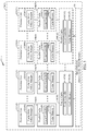
- FIG 1 is a block diagram of an exemplary multiprocessor system 10 comprising a plurality of parallel processor cores 22(0)-22(X). Each processing core 22(0)-22(X) accesses a local parallel cache 14(0)-14(X) comprising a cache controller 16(0)-16(X) and a cache memory 18(0)-18(X).
- the caches 14(0)-14(X) in Figure 1 are parallel caches, because they share a common lineage shared memory 20. As illustrated in Figure 1 , the parallel caches 14(0)-14(X) may be first-level caches for the processors cores 22(0)-22(X). Alternatively, the parallel caches 14(0)-14(X) may be higher-level caches, for example second-level or third-level caches of the processor cores 22(0)-22(X).
- the parallel caches 14(0)-14(X) share a shared memory 20.
- the shared memory 20 may be a shared cache, for example, a second-level cache.
- the shared memory 20 may also be a main memory.
- the multiprocessor system 10 may be integrated into a semiconductor die 24.
- a multiprocessor system may spend some of its operating time having a single processor core active. Therefore, it may be beneficial to optimize the multiprocessor system 10 to consume less power when operating with a single processor core 22(0) active. From time to time, when increased performance is required, one or more other processor cores 22(X) of the multiprocessor system 10 may be activated to provide increased processing capacity for the multiprocessor system 10. Additional power may be consumed by the multiprocessor system 10 when more than one of the processor cores 22(0)-22(X) are active; however, the increased power consumed by the multiprocessor system 10 may only occur during periods of time when increased bursts of performance may be required.
- the multiprocessor system 10 comprises a cache write policy manager 12 configured to provide a hybrid write-through/write-back cache policy.
- the cache write policy manager 12 is configured to manage the cache write policy of a plurality of parallel caches 14(0)-14(X).
- the cache write policy manager 12 is configured to determine whether at least two parallel caches 14(0)-14(X) are active.
- the cache write policy manager 12 is configured to instruct an active cache 14(0) among the plurality of parallel caches 14(0)-14(X) to apply a write-back cache policy if all of one or more other caches 14(X) among the plurality of parallel caches 14(0)-14(X) are not active.
- the cache write policy manager 12 may conserve power and/or increase performance of the multiprocessor system 10 when only a single processor core 22(0) among a plurality of parallel processor cores 22(0)-22(X) is active.
- the cache write policy manager 12 may be configured to instruct the active cache 14(0) among the plurality of parallel caches 14(0)-14(X) to apply a write-back cache policy when all of the other caches 14(X) among the plurality of parallel caches 14(0)-14(X) become inactive.
- the cache write policy manager 12 is also configured to instruct an active cache 14(0) among the plurality of parallel caches 14(0)-14(X) to apply a write-through cache policy if any of the one or more other caches 14(X) are active. In this manner, the cache write policy manager 12 facilitates data coherency among the parallel caches 14(0)-14(X) when multiple processor cores 22(0)-22(X) among the plurality of parallel processor cores 22(0)-22(X) are active.
- the cache write policy manager 12 is configured to send instructions to the cache controllers 16(0)-16(X) of the parallel caches 14(0)-14(X) to implement the hybrid write-through/write-back cache policy.
- the cache write policy manager 12 is configured to instruct the desired cache write policy to be set for the parallel caches 14(0)-14(X).
- the cache controller 16(0) is configured to receive the instructions from the cache write policy manager 12 to set the desired cache write policy for the cache memory 18(0).
- the cache controller 16(0) is configured to set a write-back cache policy as the cache write policy for the cache memory 18(0) in response to receipt of an indication that all of one or more other caches 14(X) among a plurality of parallel caches 14(0)-14(X) are not active.
- the cache controller 16(0) is further configured to set a write-through cache policy for the cache memory 18(0) in response to receipt of an indication that any of the one or more other caches 14(X) among the plurality of parallel caches 14(0)-14(X) are active.
- the cache write policy manager 12 may be implemented as a state machine.
- Figure 2 provides an exemplary state machine 26 that may be performed by the cache write policy manager 12 of Figure 1 .
- Figure 2 illustrates an exemplary state machine 26 for a cache write policy manager 12.
- the state machine 26 may be provided having a first state 28, a second state 30, a third state 32, and a fourth state 34.
- the local cache 14(0) accessed by the processor core 22(0) may be the only active cache among a plurality of parallel caches 14(0)-14(X).
- the cache write policy manager 12 when only one cache 14(0) is active, the cache write policy manager 12 will be in a first state 28. In the first state 28, the cache write policy manager 12 applies a write-back cache policy to the active cache 14(0). When applying the write-back cache policy, the cache 14(0) can store dirty data.
- the cache write policy manager 12 detects that any of the one or more other caches 14(X) are active, the cache write policy manager 12 transitions from the first state 28 to a second state 30.
- the cache write policy manager 12 may be configured to determine that any of the one or more other caches 14(X) among the plurality of parallel caches 14(0)-14(X) are active by determining that any of the one or more other caches 14(X) are powered.
- the cache write policy manager 12 may also be configured to determine that any of the one or more other caches 14(X) are active by determining that any of the one or more other processor cores 22(X) configured to access any of the one or more other caches 14(X) are powered and/or active.
- the cache write policy manager 12 makes the initially active cache 14(0) coherent with the one or more other caches 14(X). To achieve data coherency, the cache write policy manager 12 instructs the initially active cache 14(0) to clean all dirty cache lines.
- the active cache 14(0) may clean all dirty cache lines by writing data stored by any dirty cache lines to a shared memory 20 shared among the plurality of parallel caches 14(0)-14(X).
- the cache write policy manager 12 Before, during, or after cleaning all the dirty cache lines to the shared memory 20, the cache write policy manager 12 also instructs the initially active cache 14(0) to apply a write-through cache policy.
- the cache write policy manager 12 will also instruct the one or more other caches 14(X) to apply a write-through cache policy.
- the cleaning of the dirty cache lines of the cache 14(0) may be completed before a newly activating other processor core 22(X) and/or before the newly activating one or more other caches 14(X) become fully active.
- the initially active cache 14(0) of the first processor core 22(0) will thereafter maintain coherency with the one or more other caches 14(X). Coherency is maintained through the shared memory 20 in this embodiment.
- the common lineage shared memory 20 may be a next-level shared memory of the active cache 14(0) and/or the other caches 14(X). Alternatively, there may be one or more intermediate cache(s) and/or intermediate memory(ies) disposed between the active cache 14(0) and the shared memory 20.
- the operations of the second state 30 may be instructed to occur substantially in parallel with the activating of the one or more other processor cores 22(X) and/or the activating of the one or more other caches 14(X).
- the cache write policy manager 12 transitions to a third state 32.
- the third state 32 there are at least two parallel caches 14 (e.g., 14(0), 14(X)) active and each of the active parallel caches 14 is applying a write-through cache policy. This allows the active processor cores 22(0)-22(X) to maintain coherency of the active caches 14(0)-14(X) in the shared memory 20 in this embodiment.
- the cache write policy manager 12 remains in the third state 32 and the additional other cache(s) 14(X) are also instructed to apply a write-through cache policy.
- the additional processing capacity of the one or more other processor cores 22(X) may no longer be required by the multiprocessor system 10.
- the multiprocessor system 10 may instruct the one or more other processor cores 22(X) to deactivate in order to conserve power.
- the one or more other caches 14(X) may also be powered down and/or deactivated (i.e., made not active) without flushing the one or more other caches 14(X) to the shared memory 20.
- the cache policy manager 12 determines that all of the one or more other caches 14(X) are not active (e.g., only one cache 14(0) remains active)
- the cache write policy manager 12 transitions from the third state 32 to the fourth state 34.
- the cache write policy manager 12 instructs the remaining active cache 14(0) to apply a write-back cache policy. Dirty data may again be stored in the cache 14(0). As a result, less power is consumed by the multiprocessor system 10. Also, depending on implementation, workload, and/or other design factors, the remaining active processor core 22(0) could have an increased performance under the write-back cache policy.
- the cache write policy manager 12 transitions from the fourth state 34 to the first state 28.
- the cache write policy manager 12 will remain in the first state 28 as long as the active parallel cache 14(0) is the only active cache 14 among the plurality of parallel caches 14(0)-14(X). The cache write policy manager 12 thereafter continues as herein discussed.
- the remaining singly active cache 14(0) at the end of a cycle through the first, second, third, and fourth states of the state machine 26 may be a same cache 14 or a different cache 14 among the plurality of parallel caches 14(0)-14(X) than the initially active cache 14(0) at the beginning of the cycle.
- a same cache 14 or a different cache 14 may remain active at the end of the cycle through the state machine 26 than was initially active at the beginning of the cycle through the state machine 26.
- the cache write policy manager 12 may comprise and operate several state machines 26.
- a cache write policy manager 12 managing multiple caches 14 may comprise and operate a separate state machine 26 for each cache 14 managed by the cache write policy manager 12.
- the previous discussion refers to four separate states of the state machine 26: the first state 28, the second state 30, the third state 32, and the fourth state 34.
- the first state 28 and third state 32 may be longer duration states
- the second state 30 and the fourth state 34 may be transitional (i.e., lesser duration) states.
- the state machine 26 may also be provided with fewer or additional states.
- the state machine 26 may be provided as a two-state machine, with the longer duration first state 28 and the transitional second state 30 being provided as a first state 36, and with the longer duration third state 32 and the transitional fourth state 34 being provided as a second state 38.
- an optional fifth startup state 40 illustrated in Figure 2 is now discussed.
- the cache write policy manager 12 may not initially know whether other parallel caches 14 are active. Before a determination of which caches 14 are active/not active can be made, it may be unsafe to assume an activating cache 14 is the only active cache 14. Accordingly, the cache write policy manager 12 may be configured to instruct a cache 14 to apply the write-through cache policy as the default cache write policy until a determination of which caches 14 are active/not active can be made. As a result, data coherency issues are avoided that could otherwise occur if the activating cache 14 applied a write-back cache policy in the presence of other active parallel caches 14.
- the cache write policy manager 12 may initially start in the startup state 40.
- the cache write policy manager 12 instructs the cache 14 to apply a write-through cache policy.
- the cache write policy manager 12 then transitions to the third state 32.
- a determination will then be made regarding which caches 14 are active/not active. If all of the one or more other caches 14(X) among the plurality of parallel caches 14 are not active, then the cache write policy manager 12 of the activating cache 14 will transition to the fourth state 34 (instructing the activating cache 14 to apply a write-back cache policy) and then transition to the first state 28. If any of the one or more other caches 14(X) among the plurality of parallel caches 14 are active, then the cache write policy manager 12 of the activating cache 14 will remain in the third state 38.
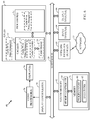
- the multiprocessor system 10 of Figure 1 illustrates a single cluster of processor cores 22(0)-22(X). However, the multiprocessor system 10 may also be provided as a part of a hierarchical multiprocessor system 10(1).
- Figure 3 illustrates a hierarchical multiprocessor system 10(1) having a plurality of processor core clusters.
- the processor cores 22A(0)-22A(X) provide a first cluster of processor cores.
- the processor cores 22B(0)-22B(Y) form a second processor core cluster.
- the caches 14A(0)-14A(X) are parallel caches, because they share a common lineage parallel cache 14C(0).
- the caches 14B(0)-14B(Y) are parallel caches, because they share a common lineage parallel cache 14C(Z).
- the caches 14C(0)-14C(Z) are parallel caches, because they share a common lineage shared memory 20.
- the caches 14A(0)-14A(X) and 14B(0)-14B(X) are also parallel caches because they share a common lineage shared memory 20.
- the hierarchical multiprocessor system 10(1) may be provided on a semiconductor die 24(1).
- the elements in Figure 3 have similar element numbers to the elements of Figure 1 and operate in the same manner as the elements in Figure 1 , except whereas herein described.
- the cache write policy manager 12 of Figure 1 may be provided as a plurality of cache write policy managers 12A(0)-12A(X), 12B(0)-12B(Y).
- each processor core 22 e.g., processor cores 22A(0)-22A(X) and 22B(0)-22B(Y)
- contains a cache write policy manager 12 e.g., 12A(0)-12A(X) and 12B(0)-12B(Y), respectively.
- the cache write policy manager 12 contained in each processor core 22 is configured to determine whether at least two caches 14 among the plurality of parallel caches 14A(0)-14A(X), 14B(0)-14B(Y) are active.
- the cache write policy manager 12 contained in each processor core 22 is also configured to instruct a parallel cache 14 accessed by its processor core 22, regarding which cache write policy to apply.
- cache write policy manager 12A(0) may instruct the parallel cache 14A(0) to apply a write-back cache policy.
- the cache write policy manager 12A(0) may also instruct the parallel cache 14A(0) to apply a write-back cache policy if none of the one or more other processor cores 22B(0)-22B(Y) in the second processor core cluster are active.
- processor core 22A(X) powers on, the cache write policy manager 12A(X) determines that the parallel cache 14A(0) is already active and therefore instructs the parallel cache 14A(X) to apply a write-through cache policy.
- the cache write policy manager 12A(0) When the processor core 22A(X) powers up, the cache write policy manager 12A(0) also determines that the processor core 22A(X) is activating and therefore instructs the already active cache 14A(0) to clean its cache lines of all dirty data. The parallel cache 14A(X) will then clean all of its dirty cache lines by writing data stored in any dirty cache lines of the parallel cache 14A(0) to a parallel cache 14C(0) shared between the processor cores 22A(0)-22A(X) of the first processor core cluster.
- the parallel cache 14A(0) is prepared to maintain data coherency with the parallel cache 14A(X) of the processor core 22A(X).
- both parallel caches 14A(0), 14A(X) will apply a write-through cache policy to write any data stored in their local cache memories 18A(0), 18A(X) to the parallel cache 14C(0).
- the state machine 26 of Figure 2 may also be applied to parallel caches, such as parallel caches 14C(0)-14C(Z).
- parallel caches such as parallel caches 14C(0)-14C(Z).
- processor cores 22 active in a first processor cluster (e.g., processor cores 22A(0), 22A(X)).
- processor cores 22B(0)-22B(Y) active in one or more other processor clusters.
- a parallel cache 14C(0) is active and there are no other parallel cache(s) 14C(Z) active.
- the parallel cache 14C(0) is instructed to apply a write-back cache policy.
- the parallel cache 14C(0) may continue to apply a write-back cache policy for as long as all other parallel caches (e.g., the parallel cache 14C(Z)) parallel to the parallel cache 14C(0) remain inactive (i.e., not active).
- the state machine 26 of Figure 2 is used to set the policies of the parallel caches 14C(0)-14C(Z) in a deeper cache level.
- the parallel cache 14B(0) and the parallel cache 14C(Z) will also power on and become active.
- the cache write policy manager 12B(0) determines that the parallel caches 14A(0)-14A(X) are active and therefore instructs the parallel cache 14B(0) to apply a write-through cache policy.
- the cache write policy manager 12B(0) also determines that the parallel cache 14C(0) is active and therefore instructs the parallel cache 14C(Z) to apply a write-through cache policy.
- the cache write policy manager 12A(0) also determines that the processor core 22B(0) and/or the parallel cache 14B(0) is active and therefore instructs the parallel cache 14C(0) to apply a write-through cache policy. This allows the parallel cache 14C(0) to maintain coherency with the newly activated parallel cache 14C(Z). In this regard, the parallel cache 14C(0) and the parallel cache 14C(Z) will each write-through data stored in their cache memories 18C(0), 18C(Z) to the shared memory 20.
- the cache write policy manager 12A(0) When all active processor cores 22B of the other processor core cluster (processor core 22B(0) in this example) are deactivated, the cache write policy manager 12A(0) will determine that no other processor cores 22B(0)-22B(Y) and/or parallel caches 14B(0)-14B(Y) of any other processor core clusters are active. When this occurs, the cache write policy manager 12A(0) may instruct the parallel cache 14C(0) to apply a write-back cache policy. Applying a write-back cache policy may conserve power and/or enhance the performance of the processors 12A(0)-12A(X) in the only remaining active processor core cluster (i.e., processors 12A(0)-12A(X)).
- each processor core cluster in Figure 3 may comprise two or more processor cores 22.
- the hierarchical multiprocessor system 10(1) may comprise two or more processor core clusters.
- the hierarchical multiprocessor system 10(1) illustrated in Figure 3 illustrates three levels of caches.
- the state machine 26 may also be applied to deeper cache hierarchies.
- FIG. 3 illustrates a multiprocessor system 10(2) comprising a cache write policy manager 12 integrated into a hypervisor 44.
- the hypervisor 44 can determine whether any of the processor cores 22A(0)-22A(X), 22B(0)-22B(Y) and/or parallel caches 14A(0)-14A(X), 14B(0)-14B(Y) are active.
- the hypervisor may also determine whether any of the parallel caches 14C(0)-14C(Z) are active.
- the hypervisor 44 may also control the activation and deactivation of the processors cores 22A(0)-22A(X), 22B(0)-22B(Y), and/or the activation and deactivation of their respective processor core clusters.
- the hypervisor 44 is provided as separate circuitry on a semiconductor die 24(2).
- the hypervisor 44 is provided in software. When implemented in software, the hypervisor 44 may execute on a separate processor core 22 from the processor cores 22A(0)-22A(X), 22B(0)-22B(Y). However, the hypervisor 44 may also execute on one or more of the processor cores 22A(0)-22A(X), 22B(0)-22B(Y).
- the cache write policy manager 12 may also be integrated into a power management unit (PMU) 46.
- the PMU 46 may be implemented as separate circuitry of a semiconductor die 24(3).
- the PMU 46 controls the powering on and/or powering off of processor cores 22A(0)-22A(X), 22B(0)-22B(Y) and/or parallel caches 14A(0)-14A(X), 14B(0)-14B(Y).
- the PMU 46 may or may not implement separate state machines 26 for affecting parallel caches 14A(0)-14A(X), 14B(0)-14B(Y) and/or parallel caches 14C(0)-14C(Z).
- the cache write policy manager 12 and/or parallel caches 14, may be provided in or integrated into any processor-based device. Examples, without limitation, include a set top box, an entertainment unit, a navigation device, a communications device, a fixed location data unit, a mobile location data unit, a mobile phone, a cellular phone, a computer, a portable computer, a desktop computer, a personal digital assistant (PDA), a monitor, a computer monitor, a television, a tuner, a radio, a satellite radio, a music player, a digital music player, a portable music player, a digital video player, a video player, a digital video disc (DVD) player, and a portable digital video player.
- PDA personal digital assistant
- FIG. 6 illustrates an example of a processor-based system 48.
- the processor-based system 48 includes one or more central processing units (CPU(s)) 50, each including one or more processors 52.
- the CPU(s) 50 may have cache(s) 53 coupled to the processor(s) 52 for rapid access to temporarily stored data.
- each cache 53 may contain a cache controller 56 and cache memory 54, controlled as herein discussed.
- the CPU(s) 50 is coupled to a system bus 58 and can intercouple master devices and slave devices included in the processor-based system 48.
- the CPU(s) 50 communicates with these other devices by exchanging address, control, and data information over the system bus 58.
- the CPU(s) 50 can communicate bus transaction requests to the memory controller 60, as an example of a slave device.
- multiple system buses 58 could be provided, wherein each system bus 58 constitutes a different fabric.
- Other master and slave devices can be coupled to the system bus 58. As illustrated in Figure 6 , these devices can include a system memory 62, one or more input devices 64, one or more output devices 66, one or more network interface devices 68, and one or more display controllers 70, as examples.
- the input device(s) 64 can include any type of input device, including but not limited to input keys, switches, voice processors, etc.
- the output device(s) 66 can include any type of output device, including but not limited to audio, video, other visual indicators, etc.
- the network interface device(s) 68 can be any device(s) configured to allow exchange of data to and from a network 72.
- the network 72 can be any type of network, including but not limited to a wired or wireless network, a private or public network, a local area network (LAN), a wide local area network (WLAN), and the Internet.
- the network interface device(s) 68 can be configured to support any type of communication protocol desired.
- the CPU(s) 50 may also include one or more cache write policy managers 12.
- the one or more cache write policy managers 12 may be integral to the cache(s) 53 and/or integral to the processor(s) 52.
- the one or more cache write policy managers 12 may also be provided in the CPU(s) 50 separately from the cache(s) 53 and/or processor(s) 52.
- one or more separately-provided cache write policy managers 12 may be provided integral to a hypervisor 44 and/or a PMU 46 of the CPU(s) 50.
- the CPU(s) 50 may also be configured to access the display controller(s) 70 over the system bus 58 to control information sent to one or more displays 74.
- the display controller(s) 70 send information to the display(s) 74 to be displayed via one or more video processors 76, which process the information to be displayed into a format suitable for the display(s) 74.
- the display(s) 74 can include any type of display, including but not limited to a cathode ray tube (CRT), a liquid crystal display (LCD), a plasma display, etc.
- the system memory 62 may comprise a memory controller 60 for accessing memory 78 of the processor-based system 48.
- the memory 78 may comprise a non-transitory computer-readable medium.
- the computer-readable medium may have stored thereon computer-executable instructions to cause the processor(s) 52 to implement methods herein described for providing a hybrid write-through/write-back cache policy for one or more of a plurality of caches 53.
- the memory 78 may comprise a program store 80 and/or a data store 82.
- a processing core (herein also called a core, processing core, and/or processor) may be a microprocessor, but in the alternative, the processing core may be any conventional processor, controller, microcontroller, or state machine.
- a processing core may also be implemented as a combination of computing devices, e.g., a combination of a DSP and a microprocessor, a plurality of microprocessors, one or more microprocessors in conjunction with a DSP core, or any other such configuration.
- RAM Random Access Memory
- ROM Read Only Memory
- EPROM Electrically Programmable ROM
- EEPROM Electrically Erasable Programmable ROM
- registers a hard disk, a removable disk, a CD-ROM, or any other form of computer-readable medium known in the art.
- An exemplary storage medium is coupled to the processor such that the processor can read information from, and write information to, the storage medium.
- the storage medium may be integral to the processor.
- the processor and the storage medium may reside in an ASIC.
- the ASIC may reside in a remote station.
- the processor and the storage medium may reside as discrete components in a remote station, base station, or server.
Landscapes
- Engineering & Computer Science (AREA)
- Theoretical Computer Science (AREA)
- General Engineering & Computer Science (AREA)
- Physics & Mathematics (AREA)
- General Physics & Mathematics (AREA)
- Computer Hardware Design (AREA)
- Computing Systems (AREA)
- Memory System Of A Hierarchy Structure (AREA)
Applications Claiming Priority (3)
| Application Number | Priority Date | Filing Date | Title |
|---|---|---|---|
| US201261586937P | 2012-01-16 | 2012-01-16 | |
| US13/470,643 US10025711B2 (en) | 2012-01-16 | 2012-05-14 | Hybrid write-through/write-back cache policy managers, and related systems and methods |
| PCT/US2013/021774 WO2013109648A1 (en) | 2012-01-16 | 2013-01-16 | Hybrid write-through/write-back cache policy managers, and related systems and methods |
Publications (2)
| Publication Number | Publication Date |
|---|---|
| EP2805243A1 EP2805243A1 (en) | 2014-11-26 |
| EP2805243B1 true EP2805243B1 (en) | 2016-03-23 |
Family
ID=48780824
Family Applications (1)
| Application Number | Title | Priority Date | Filing Date |
|---|---|---|---|
| EP13701347.0A Not-in-force EP2805243B1 (en) | 2012-01-16 | 2013-01-16 | Hybrid write-through/write-back cache policy managers, and related systems and methods |
Country Status (9)
| Country | Link |
|---|---|
| US (1) | US10025711B2 (es) |
| EP (1) | EP2805243B1 (es) |
| JP (1) | JP5960842B2 (es) |
| KR (2) | KR20170016995A (es) |
| CN (1) | CN104067243B (es) |
| ES (1) | ES2573284T3 (es) |
| HU (1) | HUE028928T2 (es) |
| TW (1) | TWI489277B (es) |
| WO (1) | WO2013109648A1 (es) |
Families Citing this family (25)
| Publication number | Priority date | Publication date | Assignee | Title |
|---|---|---|---|---|
| US9372803B2 (en) * | 2012-12-20 | 2016-06-21 | Advanced Micro Devices, Inc. | Method and system for shutting down active core based caches |
| US9442849B2 (en) * | 2012-12-29 | 2016-09-13 | Intel Corporation | Apparatus and method for reduced core entry into a power state having a powered down core cache |
| US10216640B2 (en) * | 2014-03-21 | 2019-02-26 | Samsung Electronics Co., Ltd. | Opportunistic cache injection of data into lower latency levels of the cache hierarchy |
| US9594628B2 (en) | 2014-07-30 | 2017-03-14 | Segate Technology Llc | Operational vibration compensation through media cache management |
| US9740426B2 (en) * | 2014-09-19 | 2017-08-22 | Lenovo (Singapore) Pte. Ltd. | Drive array policy control |
| US10019362B1 (en) * | 2015-05-06 | 2018-07-10 | American Megatrends, Inc. | Systems, devices and methods using solid state devices as a caching medium with adaptive striping and mirroring regions |
| US10089227B1 (en) | 2015-05-06 | 2018-10-02 | American Megatrends, Inc. | Systems, devices and methods using a solid state device as a caching medium with a write cache flushing algorithm |
| US10108344B1 (en) | 2015-05-06 | 2018-10-23 | American Megatrends, Inc. | Systems, devices and methods using a solid state device as a caching medium with an SSD filtering or SSD pre-fetch algorithm |
| US10176103B1 (en) | 2015-05-07 | 2019-01-08 | American Megatrends, Inc. | Systems, devices and methods using a solid state device as a caching medium with a cache replacement algorithm |
| US10114566B1 (en) | 2015-05-07 | 2018-10-30 | American Megatrends, Inc. | Systems, devices and methods using a solid state device as a caching medium with a read-modify-write offload algorithm to assist snapshots |
| US10055354B1 (en) | 2015-05-07 | 2018-08-21 | American Megatrends, Inc. | Systems, devices and methods using a solid state device as a caching medium with a hashing algorithm to maintain sibling proximity |
| CN105740170B (zh) * | 2016-01-22 | 2020-12-04 | 浪潮(北京)电子信息产业有限公司 | 一种缓存脏页刷写方法及装置 |
| US9990286B1 (en) * | 2017-05-05 | 2018-06-05 | Honeywell International, Inc. | Memory tracking using copy-back cache for 1:1 device redundancy |
| KR102430983B1 (ko) * | 2017-09-22 | 2022-08-09 | 삼성전자주식회사 | 스토리지 장치 및 그 동작 방법 |
| KR20190067370A (ko) * | 2017-12-07 | 2019-06-17 | 에스케이하이닉스 주식회사 | 데이터 저장 장치 및 동작 방법, 이를 포함하는 스토리지 시스템 |
| CN108052414B (zh) * | 2017-12-28 | 2021-09-17 | 湖南国科微电子股份有限公司 | 一种提升ssd工作温度范围的方法及系统 |
| TWI681293B (zh) * | 2018-01-10 | 2020-01-01 | 瑞昱半導體股份有限公司 | 暫存記憶體處理方法、暫存記憶體程式與記憶裝置 |
| JP6995644B2 (ja) * | 2018-01-23 | 2022-01-14 | 日立Astemo株式会社 | 電子制御装置 |
| KR102052312B1 (ko) * | 2018-05-08 | 2019-12-05 | 주식회사 애포샤 | 캐싱 장치 및 방법 |
| KR20200056548A (ko) | 2018-11-14 | 2020-05-25 | 에스케이하이닉스 주식회사 | 캐시 시스템을 갖는 메모리 시스템 및 메모리 시스템에서의 캐싱 동작 제어방법 |
| KR20210066631A (ko) | 2019-11-28 | 2021-06-07 | 삼성전자주식회사 | 메모리에 데이터를 기입하기 위한 장치 및 방법 |
| US11023375B1 (en) * | 2020-02-21 | 2021-06-01 | SiFive, Inc. | Data cache with hybrid writeback and writethrough |
| US11567873B1 (en) * | 2021-09-27 | 2023-01-31 | Sap Se | Extended cache for efficient object store access by a database |
| KR102641481B1 (ko) * | 2023-04-19 | 2024-02-28 | 메티스엑스 주식회사 | 멀티프로세서 시스템 및 이의 데이터 관리 방법 |
| KR102570030B1 (ko) * | 2023-04-19 | 2023-08-28 | 메티스엑스 주식회사 | 멀티프로세서 시스템 및 이의 데이터 관리 방법 |
Family Cites Families (20)
| Publication number | Priority date | Publication date | Assignee | Title |
|---|---|---|---|---|
| JPH01266643A (ja) * | 1988-04-18 | 1989-10-24 | Nippon Telegr & Teleph Corp <Ntt> | キャッシュ制御方式 |
| JP2533612B2 (ja) | 1988-05-16 | 1996-09-11 | 富士通株式会社 | メモリのデ―タ保護方式 |
| JPH04347749A (ja) * | 1991-05-24 | 1992-12-02 | Nec Corp | 情報処理装置 |
| US5301298A (en) | 1991-10-11 | 1994-04-05 | Intel Corporation | Processor for multiple cache coherent protocols |
| US5522057A (en) | 1993-10-25 | 1996-05-28 | Intel Corporation | Hybrid write back/write through cache having a streamlined four state cache coherency protocol for uniprocessor computer systems |
| US6052789A (en) | 1994-03-02 | 2000-04-18 | Packard Bell Nec, Inc. | Power management architecture for a reconfigurable write-back cache |
| JPH0883215A (ja) * | 1994-09-12 | 1996-03-26 | Hitachi Ltd | メモリ制御装置 |
| US6571324B1 (en) * | 1997-06-26 | 2003-05-27 | Hewlett-Packard Development Company, L.P. | Warmswap of failed memory modules and data reconstruction in a mirrored writeback cache system |
| US6711691B1 (en) | 1999-05-13 | 2004-03-23 | Apple Computer, Inc. | Power management for computer systems |
| US6725342B1 (en) * | 2000-09-26 | 2004-04-20 | Intel Corporation | Non-volatile mass storage cache coherency apparatus |
| US7127560B2 (en) | 2003-10-14 | 2006-10-24 | International Business Machines Corporation | Method of dynamically controlling cache size |
| US7173863B2 (en) | 2004-03-08 | 2007-02-06 | Sandisk Corporation | Flash controller cache architecture |
| US20080008256A1 (en) * | 2004-08-02 | 2008-01-10 | Matshushita Electric Industrial Co., Ltd. | Ofdm Transmitting Apparatus, Ofdm Receiving Apparatus, and Their Methods |
| US7624236B2 (en) * | 2004-12-27 | 2009-11-24 | Intel Corporation | Predictive early write-back of owned cache blocks in a shared memory computer system |
| US7849350B2 (en) * | 2006-09-28 | 2010-12-07 | Emc Corporation | Responding to a storage processor failure with continued write caching |
| US7730248B2 (en) * | 2007-12-13 | 2010-06-01 | Texas Instruments Incorporated | Interrupt morphing and configuration, circuits, systems and processes |
| US8145932B2 (en) * | 2008-06-30 | 2012-03-27 | Dell Products L.P. | Systems, methods and media for reducing power consumption in multiple controller information handling systems |
| US8161247B2 (en) * | 2009-06-26 | 2012-04-17 | Microsoft Corporation | Wait loss synchronization |
| US8751833B2 (en) | 2010-04-30 | 2014-06-10 | Arm Limited | Data processing system |
| WO2013054374A1 (en) * | 2011-10-12 | 2013-04-18 | Hitachi, Ltd. | Storage system, and data backup method and system restarting method of storage system |
-
2012
- 2012-05-14 US US13/470,643 patent/US10025711B2/en active Active
-
2013
- 2013-01-16 EP EP13701347.0A patent/EP2805243B1/en not_active Not-in-force
- 2013-01-16 HU HUE13701347A patent/HUE028928T2/en unknown
- 2013-01-16 KR KR1020177002768A patent/KR20170016995A/ko not_active Application Discontinuation
- 2013-01-16 KR KR1020147022679A patent/KR101747894B1/ko active IP Right Grant
- 2013-01-16 TW TW102101719A patent/TWI489277B/zh active
- 2013-01-16 WO PCT/US2013/021774 patent/WO2013109648A1/en active Application Filing
- 2013-01-16 CN CN201380005469.8A patent/CN104067243B/zh not_active Expired - Fee Related
- 2013-01-16 JP JP2014552397A patent/JP5960842B2/ja not_active Expired - Fee Related
- 2013-01-16 ES ES13701347.0T patent/ES2573284T3/es active Active
Also Published As
| Publication number | Publication date |
|---|---|
| HUE028928T2 (en) | 2017-01-30 |
| US10025711B2 (en) | 2018-07-17 |
| ES2573284T3 (es) | 2016-06-07 |
| CN104067243B (zh) | 2017-09-12 |
| CN104067243A (zh) | 2014-09-24 |
| JP5960842B2 (ja) | 2016-08-02 |
| KR20170016995A (ko) | 2017-02-14 |
| JP2015503816A (ja) | 2015-02-02 |
| TW201342062A (zh) | 2013-10-16 |
| US20130185511A1 (en) | 2013-07-18 |
| EP2805243A1 (en) | 2014-11-26 |
| KR20140116495A (ko) | 2014-10-02 |
| WO2013109648A1 (en) | 2013-07-25 |
| KR101747894B1 (ko) | 2017-06-15 |
| TWI489277B (zh) | 2015-06-21 |
Similar Documents
| Publication | Publication Date | Title |
|---|---|---|
| EP2805243B1 (en) | Hybrid write-through/write-back cache policy managers, and related systems and methods | |
| JP5367899B2 (ja) | 低電力モード中にキャッシュされた情報を保存する技術 | |
| US8689017B2 (en) | Server power manager and method for dynamically managing server power consumption | |
| US8656196B2 (en) | Hardware automatic performance state transitions in system on processor sleep and wake events | |
| US7590815B1 (en) | Method and apparatus for partial memory power shutoff | |
| US10539997B2 (en) | Ultra-low-power design memory power reduction scheme | |
| TW201403465A (zh) | 多cpu系統以及具有該多cpu系統的計算系統 | |
| JP2016506576A (ja) | 集積回路のアイドルフェーズ予測 | |
| DE112006002835T5 (de) | Verfahren und System zum Optimieren der Latenz bei dynamischer Speichereinteilung | |
| JP2012150815A (ja) | 複数の回路における性能パラメータの整合 | |
| US11922172B2 (en) | Configurable reduced memory startup | |
| US20220188208A1 (en) | Methods for configuring span of control under varying temperature | |
| US9823730B2 (en) | Power management of cache duplicate tags | |
| US10318428B2 (en) | Power aware hash function for cache memory mapping | |
| US20230004400A1 (en) | System and method for providing system level sleep state power savings | |
| US9411663B2 (en) | Conditional notification mechanism | |
| US20230086149A1 (en) | Reducing memory power usage in far memory | |
| JP2021515305A (ja) | スコアボードの保存及び復元 |
Legal Events
| Date | Code | Title | Description |
|---|---|---|---|
| PUAI | Public reference made under article 153(3) epc to a published international application that has entered the european phase |
Free format text: ORIGINAL CODE: 0009012 |
|
| 17P | Request for examination filed |
Effective date: 20140620 |
|
| AK | Designated contracting states |
Kind code of ref document: A1 Designated state(s): AL AT BE BG CH CY CZ DE DK EE ES FI FR GB GR HR HU IE IS IT LI LT LU LV MC MK MT NL NO PL PT RO RS SE SI SK SM TR |
|
| DAX | Request for extension of the european patent (deleted) | ||
| 17Q | First examination report despatched |
Effective date: 20150423 |
|
| GRAP | Despatch of communication of intention to grant a patent |
Free format text: ORIGINAL CODE: EPIDOSNIGR1 |
|
| INTG | Intention to grant announced |
Effective date: 20151009 |
|
| GRAS | Grant fee paid |
Free format text: ORIGINAL CODE: EPIDOSNIGR3 |
|
| GRAA | (expected) grant |
Free format text: ORIGINAL CODE: 0009210 |
|
| AK | Designated contracting states |
Kind code of ref document: B1 Designated state(s): AL AT BE BG CH CY CZ DE DK EE ES FI FR GB GR HR HU IE IS IT LI LT LU LV MC MK MT NL NO PL PT RO RS SE SI SK SM TR |
|
| REG | Reference to a national code |
Ref country code: GB Ref legal event code: FG4D |
|
| REG | Reference to a national code |
Ref country code: CH Ref legal event code: EP |
|
| REG | Reference to a national code |
Ref country code: AT Ref legal event code: REF Ref document number: 783768 Country of ref document: AT Kind code of ref document: T Effective date: 20160415 |
|
| REG | Reference to a national code |
Ref country code: IE Ref legal event code: FG4D |
|
| REG | Reference to a national code |
Ref country code: DE Ref legal event code: R096 Ref document number: 602013005710 Country of ref document: DE |
|
| REG | Reference to a national code |
Ref country code: NL Ref legal event code: FP |
|
| REG | Reference to a national code |
Ref country code: ES Ref legal event code: FG2A Ref document number: 2573284 Country of ref document: ES Kind code of ref document: T3 Effective date: 20160607 |
|
| REG | Reference to a national code |
Ref country code: LT Ref legal event code: MG4D |
|
| PG25 | Lapsed in a contracting state [announced via postgrant information from national office to epo] |
Ref country code: GR Free format text: LAPSE BECAUSE OF FAILURE TO SUBMIT A TRANSLATION OF THE DESCRIPTION OR TO PAY THE FEE WITHIN THE PRESCRIBED TIME-LIMIT Effective date: 20160624 Ref country code: NO Free format text: LAPSE BECAUSE OF FAILURE TO SUBMIT A TRANSLATION OF THE DESCRIPTION OR TO PAY THE FEE WITHIN THE PRESCRIBED TIME-LIMIT Effective date: 20160623 Ref country code: HR Free format text: LAPSE BECAUSE OF FAILURE TO SUBMIT A TRANSLATION OF THE DESCRIPTION OR TO PAY THE FEE WITHIN THE PRESCRIBED TIME-LIMIT Effective date: 20160323 |
|
| REG | Reference to a national code |
Ref country code: AT Ref legal event code: MK05 Ref document number: 783768 Country of ref document: AT Kind code of ref document: T Effective date: 20160323 |
|
| PG25 | Lapsed in a contracting state [announced via postgrant information from national office to epo] |
Ref country code: RS Free format text: LAPSE BECAUSE OF FAILURE TO SUBMIT A TRANSLATION OF THE DESCRIPTION OR TO PAY THE FEE WITHIN THE PRESCRIBED TIME-LIMIT Effective date: 20160323 Ref country code: SE Free format text: LAPSE BECAUSE OF FAILURE TO SUBMIT A TRANSLATION OF THE DESCRIPTION OR TO PAY THE FEE WITHIN THE PRESCRIBED TIME-LIMIT Effective date: 20160323 Ref country code: LT Free format text: LAPSE BECAUSE OF FAILURE TO SUBMIT A TRANSLATION OF THE DESCRIPTION OR TO PAY THE FEE WITHIN THE PRESCRIBED TIME-LIMIT Effective date: 20160323 Ref country code: LV Free format text: LAPSE BECAUSE OF FAILURE TO SUBMIT A TRANSLATION OF THE DESCRIPTION OR TO PAY THE FEE WITHIN THE PRESCRIBED TIME-LIMIT Effective date: 20160323 |
|
| PG25 | Lapsed in a contracting state [announced via postgrant information from national office to epo] |
Ref country code: IS Free format text: LAPSE BECAUSE OF FAILURE TO SUBMIT A TRANSLATION OF THE DESCRIPTION OR TO PAY THE FEE WITHIN THE PRESCRIBED TIME-LIMIT Effective date: 20160723 Ref country code: EE Free format text: LAPSE BECAUSE OF FAILURE TO SUBMIT A TRANSLATION OF THE DESCRIPTION OR TO PAY THE FEE WITHIN THE PRESCRIBED TIME-LIMIT Effective date: 20160323 Ref country code: PL Free format text: LAPSE BECAUSE OF FAILURE TO SUBMIT A TRANSLATION OF THE DESCRIPTION OR TO PAY THE FEE WITHIN THE PRESCRIBED TIME-LIMIT Effective date: 20160323 |
|
| PG25 | Lapsed in a contracting state [announced via postgrant information from national office to epo] |
Ref country code: PT Free format text: LAPSE BECAUSE OF FAILURE TO SUBMIT A TRANSLATION OF THE DESCRIPTION OR TO PAY THE FEE WITHIN THE PRESCRIBED TIME-LIMIT Effective date: 20160725 Ref country code: SK Free format text: LAPSE BECAUSE OF FAILURE TO SUBMIT A TRANSLATION OF THE DESCRIPTION OR TO PAY THE FEE WITHIN THE PRESCRIBED TIME-LIMIT Effective date: 20160323 Ref country code: RO Free format text: LAPSE BECAUSE OF FAILURE TO SUBMIT A TRANSLATION OF THE DESCRIPTION OR TO PAY THE FEE WITHIN THE PRESCRIBED TIME-LIMIT Effective date: 20160323 Ref country code: SM Free format text: LAPSE BECAUSE OF FAILURE TO SUBMIT A TRANSLATION OF THE DESCRIPTION OR TO PAY THE FEE WITHIN THE PRESCRIBED TIME-LIMIT Effective date: 20160323 Ref country code: CZ Free format text: LAPSE BECAUSE OF FAILURE TO SUBMIT A TRANSLATION OF THE DESCRIPTION OR TO PAY THE FEE WITHIN THE PRESCRIBED TIME-LIMIT Effective date: 20160323 Ref country code: AT Free format text: LAPSE BECAUSE OF FAILURE TO SUBMIT A TRANSLATION OF THE DESCRIPTION OR TO PAY THE FEE WITHIN THE PRESCRIBED TIME-LIMIT Effective date: 20160323 |
|
| PG25 | Lapsed in a contracting state [announced via postgrant information from national office to epo] |
Ref country code: BE Free format text: LAPSE BECAUSE OF FAILURE TO SUBMIT A TRANSLATION OF THE DESCRIPTION OR TO PAY THE FEE WITHIN THE PRESCRIBED TIME-LIMIT Effective date: 20160323 |
|
| REG | Reference to a national code |
Ref country code: DE Ref legal event code: R097 Ref document number: 602013005710 Country of ref document: DE |
|
| REG | Reference to a national code |
Ref country code: FR Ref legal event code: PLFP Year of fee payment: 5 |
|
| PLBE | No opposition filed within time limit |
Free format text: ORIGINAL CODE: 0009261 |
|
| STAA | Information on the status of an ep patent application or granted ep patent |
Free format text: STATUS: NO OPPOSITION FILED WITHIN TIME LIMIT |
|
| REG | Reference to a national code |
Ref country code: HU Ref legal event code: AG4A Ref document number: E028928 Country of ref document: HU |
|
| PG25 | Lapsed in a contracting state [announced via postgrant information from national office to epo] |
Ref country code: DK Free format text: LAPSE BECAUSE OF FAILURE TO SUBMIT A TRANSLATION OF THE DESCRIPTION OR TO PAY THE FEE WITHIN THE PRESCRIBED TIME-LIMIT Effective date: 20160323 |
|
| PG25 | Lapsed in a contracting state [announced via postgrant information from national office to epo] |
Ref country code: BG Free format text: LAPSE BECAUSE OF FAILURE TO SUBMIT A TRANSLATION OF THE DESCRIPTION OR TO PAY THE FEE WITHIN THE PRESCRIBED TIME-LIMIT Effective date: 20160623 |
|
| 26N | No opposition filed |
Effective date: 20170102 |
|
| PG25 | Lapsed in a contracting state [announced via postgrant information from national office to epo] |
Ref country code: SI Free format text: LAPSE BECAUSE OF FAILURE TO SUBMIT A TRANSLATION OF THE DESCRIPTION OR TO PAY THE FEE WITHIN THE PRESCRIBED TIME-LIMIT Effective date: 20160323 |
|
| REG | Reference to a national code |
Ref country code: CH Ref legal event code: PL |
|
| PG25 | Lapsed in a contracting state [announced via postgrant information from national office to epo] |
Ref country code: MC Free format text: LAPSE BECAUSE OF FAILURE TO SUBMIT A TRANSLATION OF THE DESCRIPTION OR TO PAY THE FEE WITHIN THE PRESCRIBED TIME-LIMIT Effective date: 20160323 |
|
| PG25 | Lapsed in a contracting state [announced via postgrant information from national office to epo] |
Ref country code: CH Free format text: LAPSE BECAUSE OF NON-PAYMENT OF DUE FEES Effective date: 20170131 Ref country code: LI Free format text: LAPSE BECAUSE OF NON-PAYMENT OF DUE FEES Effective date: 20170131 |
|
| REG | Reference to a national code |
Ref country code: IE Ref legal event code: MM4A |
|
| PG25 | Lapsed in a contracting state [announced via postgrant information from national office to epo] |
Ref country code: LU Free format text: LAPSE BECAUSE OF NON-PAYMENT OF DUE FEES Effective date: 20170116 |
|
| REG | Reference to a national code |
Ref country code: FR Ref legal event code: PLFP Year of fee payment: 6 |
|
| PGFP | Annual fee paid to national office [announced via postgrant information from national office to epo] |
Ref country code: FI Payment date: 20171228 Year of fee payment: 6 |
|
| PG25 | Lapsed in a contracting state [announced via postgrant information from national office to epo] |
Ref country code: IE Free format text: LAPSE BECAUSE OF NON-PAYMENT OF DUE FEES Effective date: 20170116 |
|
| PGFP | Annual fee paid to national office [announced via postgrant information from national office to epo] |
Ref country code: IT Payment date: 20180111 Year of fee payment: 6 Ref country code: HU Payment date: 20171222 Year of fee payment: 6 |
|
| PG25 | Lapsed in a contracting state [announced via postgrant information from national office to epo] |
Ref country code: MT Free format text: LAPSE BECAUSE OF NON-PAYMENT OF DUE FEES Effective date: 20170116 |
|
| PG25 | Lapsed in a contracting state [announced via postgrant information from national office to epo] |
Ref country code: AL Free format text: LAPSE BECAUSE OF FAILURE TO SUBMIT A TRANSLATION OF THE DESCRIPTION OR TO PAY THE FEE WITHIN THE PRESCRIBED TIME-LIMIT Effective date: 20160323 |
|
| PG25 | Lapsed in a contracting state [announced via postgrant information from national office to epo] |
Ref country code: FI Free format text: LAPSE BECAUSE OF NON-PAYMENT OF DUE FEES Effective date: 20190116 Ref country code: CY Free format text: LAPSE BECAUSE OF FAILURE TO SUBMIT A TRANSLATION OF THE DESCRIPTION OR TO PAY THE FEE WITHIN THE PRESCRIBED TIME-LIMIT Effective date: 20160323 |
|
| PG25 | Lapsed in a contracting state [announced via postgrant information from national office to epo] |
Ref country code: HU Free format text: LAPSE BECAUSE OF NON-PAYMENT OF DUE FEES Effective date: 20190117 Ref country code: MK Free format text: LAPSE BECAUSE OF FAILURE TO SUBMIT A TRANSLATION OF THE DESCRIPTION OR TO PAY THE FEE WITHIN THE PRESCRIBED TIME-LIMIT Effective date: 20160323 |
|
| PG25 | Lapsed in a contracting state [announced via postgrant information from national office to epo] |
Ref country code: IT Free format text: LAPSE BECAUSE OF NON-PAYMENT OF DUE FEES Effective date: 20190116 |
|
| PGFP | Annual fee paid to national office [announced via postgrant information from national office to epo] |
Ref country code: FR Payment date: 20191226 Year of fee payment: 8 |
|
| PG25 | Lapsed in a contracting state [announced via postgrant information from national office to epo] |
Ref country code: TR Free format text: LAPSE BECAUSE OF FAILURE TO SUBMIT A TRANSLATION OF THE DESCRIPTION OR TO PAY THE FEE WITHIN THE PRESCRIBED TIME-LIMIT Effective date: 20160323 |
|
| PGFP | Annual fee paid to national office [announced via postgrant information from national office to epo] |
Ref country code: DE Payment date: 20191218 Year of fee payment: 8 Ref country code: NL Payment date: 20200102 Year of fee payment: 8 Ref country code: ES Payment date: 20200203 Year of fee payment: 8 |
|
| PGFP | Annual fee paid to national office [announced via postgrant information from national office to epo] |
Ref country code: GB Payment date: 20201231 Year of fee payment: 9 |
|
| REG | Reference to a national code |
Ref country code: DE Ref legal event code: R119 Ref document number: 602013005710 Country of ref document: DE |
|
| REG | Reference to a national code |
Ref country code: NL Ref legal event code: MM Effective date: 20210201 |
|
| PG25 | Lapsed in a contracting state [announced via postgrant information from national office to epo] |
Ref country code: NL Free format text: LAPSE BECAUSE OF NON-PAYMENT OF DUE FEES Effective date: 20210201 Ref country code: FR Free format text: LAPSE BECAUSE OF NON-PAYMENT OF DUE FEES Effective date: 20210131 |
|
| PG25 | Lapsed in a contracting state [announced via postgrant information from national office to epo] |
Ref country code: DE Free format text: LAPSE BECAUSE OF NON-PAYMENT OF DUE FEES Effective date: 20210803 |
|
| REG | Reference to a national code |
Ref country code: ES Ref legal event code: FD2A Effective date: 20220427 |
|
| PG25 | Lapsed in a contracting state [announced via postgrant information from national office to epo] |
Ref country code: ES Free format text: LAPSE BECAUSE OF NON-PAYMENT OF DUE FEES Effective date: 20210117 |
|
| GBPC | Gb: european patent ceased through non-payment of renewal fee |
Effective date: 20220116 |
|
| PG25 | Lapsed in a contracting state [announced via postgrant information from national office to epo] |
Ref country code: GB Free format text: LAPSE BECAUSE OF NON-PAYMENT OF DUE FEES Effective date: 20220116 |