EP2804133A1 - Packung mit RFID-Etikett und RFID-System - Google Patents
Packung mit RFID-Etikett und RFID-System Download PDFInfo
- Publication number
- EP2804133A1 EP2804133A1 EP14168172.6A EP14168172A EP2804133A1 EP 2804133 A1 EP2804133 A1 EP 2804133A1 EP 14168172 A EP14168172 A EP 14168172A EP 2804133 A1 EP2804133 A1 EP 2804133A1
- Authority
- EP
- European Patent Office
- Prior art keywords
- slit
- rfid tag
- package
- conductor
- cutting line
- Prior art date
- Legal status (The legal status is an assumption and is not a legal conclusion. Google has not performed a legal analysis and makes no representation as to the accuracy of the status listed.)
- Withdrawn
Links
Images














Classifications
-
- G—PHYSICS
- G06—COMPUTING OR CALCULATING; COUNTING
- G06K—GRAPHICAL DATA READING; PRESENTATION OF DATA; RECORD CARRIERS; HANDLING RECORD CARRIERS
- G06K7/00—Methods or arrangements for sensing record carriers, e.g. for reading patterns
- G06K7/10—Methods or arrangements for sensing record carriers, e.g. for reading patterns by electromagnetic radiation, e.g. optical sensing; by corpuscular radiation
- G06K7/10009—Methods or arrangements for sensing record carriers, e.g. for reading patterns by electromagnetic radiation, e.g. optical sensing; by corpuscular radiation sensing by radiation using wavelengths larger than 0.1 mm, e.g. radio-waves or microwaves
-
- G—PHYSICS
- G06—COMPUTING OR CALCULATING; COUNTING
- G06K—GRAPHICAL DATA READING; PRESENTATION OF DATA; RECORD CARRIERS; HANDLING RECORD CARRIERS
- G06K19/00—Record carriers for use with machines and with at least a part designed to carry digital markings
- G06K19/06—Record carriers for use with machines and with at least a part designed to carry digital markings characterised by the kind of the digital marking, e.g. shape, nature, code
- G06K19/067—Record carriers with conductive marks, printed circuits or semiconductor circuit elements, e.g. credit or identity cards also with resonating or responding marks without active components
- G06K19/07—Record carriers with conductive marks, printed circuits or semiconductor circuit elements, e.g. credit or identity cards also with resonating or responding marks without active components with integrated circuit chips
- G06K19/073—Special arrangements for circuits, e.g. for protecting identification code in memory
- G06K19/07309—Means for preventing undesired reading or writing from or onto record carriers
- G06K19/07372—Means for preventing undesired reading or writing from or onto record carriers by detecting tampering with the circuit
- G06K19/07381—Means for preventing undesired reading or writing from or onto record carriers by detecting tampering with the circuit with deactivation or otherwise incapacitation of at least a part of the circuit upon detected tampering
- G06K19/0739—Means for preventing undesired reading or writing from or onto record carriers by detecting tampering with the circuit with deactivation or otherwise incapacitation of at least a part of the circuit upon detected tampering the incapacitated circuit being part of an antenna
-
- G—PHYSICS
- G06—COMPUTING OR CALCULATING; COUNTING
- G06K—GRAPHICAL DATA READING; PRESENTATION OF DATA; RECORD CARRIERS; HANDLING RECORD CARRIERS
- G06K19/00—Record carriers for use with machines and with at least a part designed to carry digital markings
- G06K19/06—Record carriers for use with machines and with at least a part designed to carry digital markings characterised by the kind of the digital marking, e.g. shape, nature, code
- G06K19/067—Record carriers with conductive marks, printed circuits or semiconductor circuit elements, e.g. credit or identity cards also with resonating or responding marks without active components
- G06K19/07—Record carriers with conductive marks, printed circuits or semiconductor circuit elements, e.g. credit or identity cards also with resonating or responding marks without active components with integrated circuit chips
- G06K19/077—Constructional details, e.g. mounting of circuits in the carrier
- G06K19/07749—Constructional details, e.g. mounting of circuits in the carrier the record carrier being capable of non-contact communication, e.g. constructional details of the antenna of a non-contact smart card
-
- G—PHYSICS
- G06—COMPUTING OR CALCULATING; COUNTING
- G06K—GRAPHICAL DATA READING; PRESENTATION OF DATA; RECORD CARRIERS; HANDLING RECORD CARRIERS
- G06K19/00—Record carriers for use with machines and with at least a part designed to carry digital markings
- G06K19/06—Record carriers for use with machines and with at least a part designed to carry digital markings characterised by the kind of the digital marking, e.g. shape, nature, code
- G06K19/067—Record carriers with conductive marks, printed circuits or semiconductor circuit elements, e.g. credit or identity cards also with resonating or responding marks without active components
- G06K19/07—Record carriers with conductive marks, printed circuits or semiconductor circuit elements, e.g. credit or identity cards also with resonating or responding marks without active components with integrated circuit chips
- G06K19/077—Constructional details, e.g. mounting of circuits in the carrier
- G06K19/07749—Constructional details, e.g. mounting of circuits in the carrier the record carrier being capable of non-contact communication, e.g. constructional details of the antenna of a non-contact smart card
- G06K19/0775—Constructional details, e.g. mounting of circuits in the carrier the record carrier being capable of non-contact communication, e.g. constructional details of the antenna of a non-contact smart card arrangements for connecting the integrated circuit to the antenna
- G06K19/07756—Constructional details, e.g. mounting of circuits in the carrier the record carrier being capable of non-contact communication, e.g. constructional details of the antenna of a non-contact smart card arrangements for connecting the integrated circuit to the antenna the connection being non-galvanic, e.g. capacitive
-
- G—PHYSICS
- G06—COMPUTING OR CALCULATING; COUNTING
- G06K—GRAPHICAL DATA READING; PRESENTATION OF DATA; RECORD CARRIERS; HANDLING RECORD CARRIERS
- G06K19/00—Record carriers for use with machines and with at least a part designed to carry digital markings
- G06K19/06—Record carriers for use with machines and with at least a part designed to carry digital markings characterised by the kind of the digital marking, e.g. shape, nature, code
- G06K19/067—Record carriers with conductive marks, printed circuits or semiconductor circuit elements, e.g. credit or identity cards also with resonating or responding marks without active components
- G06K19/07—Record carriers with conductive marks, printed circuits or semiconductor circuit elements, e.g. credit or identity cards also with resonating or responding marks without active components with integrated circuit chips
- G06K19/077—Constructional details, e.g. mounting of circuits in the carrier
- G06K19/07749—Constructional details, e.g. mounting of circuits in the carrier the record carrier being capable of non-contact communication, e.g. constructional details of the antenna of a non-contact smart card
- G06K19/07798—Constructional details, e.g. mounting of circuits in the carrier the record carrier being capable of non-contact communication, e.g. constructional details of the antenna of a non-contact smart card part of the antenna or the integrated circuit being adapted for rupturing or breaking, e.g. record carriers functioning as sealing devices for detecting not-authenticated opening of containers
Definitions
- Embodiments of the present invention relate to a package including an RFID tag, RFID systems, and how to use of the RFID tag with the package. More specifically, embodiments of the present invention relate to a package to which an RFID tag is attached, an RFID system including a body, the RFID tag with the package, and how to use the package including the RFID tag.
- a system for transmitting information in a non-contact, RFID (Radio Frequency Identification) system is known.
- this RFID system includes an RFID tag (also referred to as “wireless tag”) and a read/write (RW) device.
- the RW device reads out information from the RFID tag and writes information into the RFID tag through wireless communications.
- RFID tags are classified into active and passive tags.
- An active tag includes a battery, and the active tag operates by power from the battery.
- a passive tag receives power from the RW device, and the passive tag operates by the received power.
- the active tag includes the battery, the active tag includes advantages with respect to a communication range and a stability of the communication, compared to those of the passive tag. On the other hand, the active tag has disadvantages such that, since the configuration of the active tag is complicated, downsizing is difficult and a cost tends to be higher.
- an RFID system uses short-wave or long-wave bands of frequency bands, and voltage is induced to the RFID tag by electromagnetic induction between an antenna coil of the RFID tag and a transmitting antenna coil of a RW device.
- An IC chip is activated by the voltage, and with the RFID tag it is possible to communicate.
- the RFID tag works only in an induction field in accordance with a RW device, and has a communication range of several tens of centimeters, approximately.
- a frequency band is a UHF band or a microwave band
- power is supplied to an IC chip of an RFID tag by a radio wave.
- the communication is performed based on a radio communication method. Therefore, in this case, the communication range is significantly improved.
- the communication range is from 1 m to 8 m, approximately.
- the package includes a package structure and a radio frequency identification tag.
- the package structure includes a metal film and a resin film, and the metal film includes a slit.
- the radio frequency identification tag includes a first conductor to be attached at one side of the slit in a width direction of the slit, a second conductor to be attached at another side of the slit in the width direction of the slit, and an IC chip to receive power through the first conductor and the second conductor.
- the package structure includes a cutting line and the radio frequency identification tag generates a communication failure when the package structure is cut along the cutting line. As a result, a user can manage opening information generated when a package is opened.
- a radio frequency identification system includes the package and a communication management device configured to perform at least one of reading out information from the tag through wireless communication and writing information into the tag through the wireless communication.
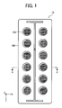
- FIG. 1 A first exemplary embodiment will be described with reference to FIG. 1 to FIG. 20 .
- a tablet sheet 10 according to the first embodiment is shown.
- FIG. 3 is a sectional view of FIG. 1 along A-A.
- plural tablets 200 are individually stored in a tablet package 100.
- the first embodiment is explained while setting a direction perpendicular to a sheet surface of the tablet sheet 10 to be a Z-axis direction in an XYZ three-dimensional orthogonal coordinate system.
- the tablet package 100 includes an RFID tag 500 and a package member 110.
- the package member 110 of a so-called PTP (Press Through Package) type includes a metal sheet 112 and a resin sheet 111.
- the resin sheet 111 includes plural tablet storing portions corresponding to a shape of a tablet 200.
- PVC polyvinyl chloride
- the metal sheet 112 is a member for sealing the tablets 200 inside each tablet storing portion of the resin sheet 111.
- an aluminum sheet is used as the metal sheet 112
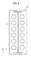
- the metal sheet 112 includes the slit SLT.
- the slit SLT includes a first slit portion S1, a second slit portion S2, and a third slit portion S3.
- the first slit portion S1 extends in a Y-axis direction.
- the second slit portion S2 extends in an X-axis direction, and the second slit portion S2 is connected to an end portion of the first slit portion S1 at a +Y side.
- the third slit portion S3 extends in an X-axis direction, and the third slit portion S3 is connected to the other end portion of the first slit portion S1 at a -Y side.
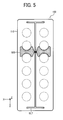
- the RFID tag 500 is a passive tag. As shown in FIG. 9 , for one example, the RFID tag 500 includes IC chip 511 and two terminal members 520. The IC chip 511 stores a unique identification (ID) number. The ID number can be read out by using the RW device.
- ID unique identification
- each of the terminal members 520 includes a thin metal film 521 and resin films 522 that cover corresponding sides of the thin metal film 521.
- the thin metal film 521 is made of an aluminum foil. (Here, the aluminum foil is utilized as the thin metal film 521).
- the thin metal film 521 of the corresponding terminal member 520 is connected to an electrode 512 of the IC chip 511.
- one of the terminal members 520 is attached to a portion of the metal sheet 112 at a +X side of the first slit portion S1, and the other of the terminal members 520 is attached to another portion of the metal sheet 112 at a -X side of the first slit portion S1.
- the thin metal films 521 of the corresponding terminal members 520 are attached to the metal sheet 112 through the resin film 522.
- the resin film 522 is adhered to the metal sheet 112 by a glue or an adhesive (e.g. a double-sided tape).
- the resin film 522 has a role as an insulator between the thin metal film 521 and the metal sheet 112, and serves to protect it from contamination or damage to the thin metal film 521.
- the impedance Z can be expressed by the formula (1) below.
- Z 1 / ⁇ ⁇ C
- ⁇ is an angular frequency
- C is a capacitance
- the angular frequency ⁇ is expressed by the formula (2) below, and the capacitance C is expressed by the formula (3) below.
- f is a frequency of the radio wave that is utilized for the communication
- S is an area of the thin metal film 521
- ⁇ 0 is a a dielectric constant of a vacuum
- ⁇ r is a dielectric constant of the isolator
- d is the thickness of the isolator.
- the electric power W supplied to the IC chip 511 from the terminal member 520 can be shown by the following formula (5).
- W a is an electric power induced between edges in the X-axis direction of the slit SLT during the communication
- V is a voltage induced between the edges in the X-axis direction of the slit SLT during the communication
- A is a current supplied from the two terminal members 520 to the IC chip 511.
- the electric power supplied to the IC chip 511 is obtained by subtracting the electric power consumed by the connecting portion (the portion of the isolator) from the electric power induced at an antenna.
- W min is a value that is uniquely determined when the type of the IC chip to be utilized and the desired communication range are determined.
- the isolator is polyethylene-telephthalate (PET)
- PET polyethylene-telephthalate
- d 20 ⁇ m
- a PET film having thickness of 20 ⁇ m is utilized as the resin film 522, and the area of each of the thin metal films 521 is substantially equal to 100 mm 2 . That is, the area of each of the thin metal films 521 is adjusted so that an alternating current having a frequency in the UHF band can flow across the first slit portion S1, even if a distance between the RW device and the RFID tag 500 is 3 m.
- Each of the terminal members 520 has a shape where portions facing the corresponding tablet storing portions are removed so as to avoid the corresponding tablet storing portions. Therefore, even if the tablet storing portion of the resin sheet 111 is pressed by a finger and the portion of the metal sheet 112 facing the tablet storing portion is broken so as to take out the tablet 200 from the package member 110, the RFID tag 500 does not receive any effect.
- the slit SLT is defined to satisfy the formula (7) below.
- L ⁇ 1 + L ⁇ 2 + L ⁇ 3 ⁇ / ⁇ r
- the width Lw of the slit SLT relates to a frequency band width, within which the slit SLT can obtain a desired gain (a good antenna performance) as an antenna. That is, as the width (Lw) becomes smaller, the frequency band width becomes smaller.
- the slit SLT is formed by a punching process using metal molds.
- the slit SLT is shaped by a secondary process depending on necessity.
- the slit SLT may be formed by laser processing. However, in this case, the cost may become higher.
- the width (Lw) is set to be within a range from 2 mm to 3 mm.
- the frequency of the radio wave used for the radio communication is 950 MHz.
- the lengths L1, L2, and L3 are defined so that L1 + L2 + L3 is equal to 160 mm.
- the width (Lw) is 3 mm.
- the RFID tag 500 is disposed at a position where impedance matching is achieved. When linearly polarized radio waves or circularly polarized radio waves are emitted from the reader/writer to the slit SLT, an electric field is generated around the slit SLT.
- the electric field generates a voltage at a portion of the metal sheet 112 at the +X side of the slit SLT and a voltage at a portion of the metal sheet 112 at the -X side of the slit SLT.
- the voltages (alternating current voltage) generated at the +X side and -X side are opposite to each other. Therefore, when the RFID tag 500 is attached to cross the slit SLT, a current flows, and the IC chip 511 of the RFID tag 500 is activated.
- the tablet package 100 includes the package member 110 and the RFID tag 500.
- the slit SLT corresponding to the wavelength of the radio wave in the UHF band is formed in the metal sheet 112 of the package member 110.
- the RFID tag 500 includes the IC chip 511 and the two terminal members 520.
- Each of the terminal members 520 includes the thin metal film 521 and the resin films 522 that cover the corresponding sides of the thin metal film 521.
- each of the thin metal films 521 is adjusted so that the alternating current having the frequency in the UHF band can flow across the slit SLT, even if the distance between the reader/writer and the RFID tag 500 is 3 m.
- the thin metal films 521 are connected to the corresponding electrodes 512 of the IC chip 511.
- One of the terminal members 520 is adhered to the portion of the metal sheet 112 at the +X side of the first slit portion S1.
- the other of the terminal members 520 is adhered to the other portion of the metal sheet 112 at the -X side of the first slit portion S1.
- radio communication in the UHF band can be ensured without reducing the communication range and without enlarging the size of the RFID tag 500.
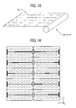
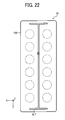
- the third embodiment is not limited to this, and the RFID tag 500 may be adhered to the resin sheet 111 (see FIGs. 21 and 22 ).
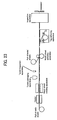
- the tag adhering apparatus is disposed at the side of the resin sheet (see FIG. 23 ).
- the thickness of the resin sheet 111 is included in the thickness d of the isolator.
- the resin film 522 may not be disposed between the thin metal films 521 and the resin sheet 111.
- the material of the resin sheet 111 is not limited to PVC.
- the metal sheet 112 is not limited to the aluminum sheet.
- a sheet containing a conductive layer may be used (for example, an alloy layer, a conductive plastic layer, a conductive polymer layer).
- the conductive plastic means a composite material with a plastic material and a conductive material having particles of inorganic conductor such as carbon fiber or metal, or having a thin film of conductor on the surface.
- the "conductive polymer” is a polymer compound having electrical conductivity. "Polyacetylene” and “Polythiazyl” are known as the conductive polymer.
- the shape of the slit SLT according to the embodiment is for exemplifying purpose only, and the shape of the slit SLT is not limited to this.
- the slit SLT may have a shape as shown in FIG. 1 .
- the formula (8) below is utilized, instead of the formula (7).
- the thin metal film 521 of the terminal member 520 is utilized as the thin metal film 521 of the terminal member 520.
- the thin metal film 521 is not limited to the aluminum foil.
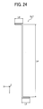
- a shape of the slits SLT is shown in FIG. 24 .
- the following formula (8) is used.
- L ⁇ 4 + L ⁇ 5 + L ⁇ 6 ⁇ / ⁇ r
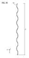
- the slit SLT may have a shape shown in FIG. 25 .
- the formula (9) below is used, instead of the formula (7).
- L ⁇ 7 ⁇ / ⁇ r
- perforations for removing at least one of the second slit S2 and the third slit S3 from the package member 110 may be formed in the package member 110 (see FIGs. 26 and 27 ).
- the radio communication between the RFID tag 500 and the RW device is disabled. Namely, the communication function of the RFID tag 500 can be easily terminated when the communication function of the RFID tag 500 becomes unnecessary.
- the tablets are medicine.
- the tablets are not limited to medicine.
- the tablets may be food.
- the package member 110 is a PTP (Press Through Package) type.
- the package member 110 is not limited to PTP.
- the package member 110 may be a member of the so-called blister type.
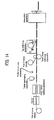
- FIG. 28 a schematic configuration of an RFID system 1000 according to the second embodiment is shown.
- RFID system 1000 is used for managing a packaging bag 40 packaging medicines, food, or electronic components (for quality control, logistic, stock).
- the RFID system 1000 includes an RFID tag 11, a reader/writer (RW) device 20, and a management device 30.
- the management device 30 and the RW device 20 can transmit and receive data with each other in wired or wireless communication.
- An RFID tag packaging bag 50 includes the packaging bag 40 (as package member) and the RFID tag 11.
- the packaging bag 40 as package member
- the RFID tag 11 As an example, two sheets 42 (same size, same shape) are overlapped and joined at an outer edge of the sheets to each other, and the packaging bag 40 is formed.
- each sheet 42 has three-layer structure consisting of a metal film 42a and two resin films 42b laminated on both surfaces of the metal film 42a.
- the sheets the metal film 42a and the resin films 42b are bonded in a stacked direction by thermal welding, ultrasonic welding, etc. For this reason, the sheet 42 has characteristics in light-shielding and waterproofing.
- the metal film 42a is composed of metal foil such as aluminum foil or copper foil.
- the material of the resin films 42b for example, is PET (polyethylene terephthalate).
- the present exemplary embodiment is described in a three-dimensional orthogonal coordinate system with an X-axis direction (in a direction of short side), a Y-axis direction (in the direction of the long side), and a Z-axis direction (in a stacking direction).
- the two sheets 42 are bonded by pressing at edge portions (+X side, -X side, and + Y side) while heating. After a content is entered from the -Y side, the two sheets 42 are sealed at the edge portion of the -Y side while heating. A label displayed information with the content in the packaging bag 40 is attached on the surface of the sheet 42 (see FIG. 28 ).
- the edge portion of the sheet 42 on the +Y side has two cutting-lines that extend in the X-axis direction and separate each other.
- Each cutting line for example, includes perforations, a half-cut line, etc.
- V-shaped notches are formed in the +X side and -X side of the packaging bag 40 on the cutting line. The user can recognize the notch easily and cut and open the packaging bag 40 quickly.
- the notches may be other shapes such as a U-shape.
- a slit SLT is formed between the two cutting lines at the edge portion of the sheet 42 on the +Y side.
- the slit has a long side in X axis direction and a short side in Y axis direction.
- the slit and the two cutting lines may be centered on an imaginary line.
- an antenna called a slot antenna (or a slit antenna) is formed in the packaging bag 40.
- the length of the slit SLT is set according to a wavelength of radio waves used in the RFID system 1000.
- the UHF band (between 300 MHz and 3 GHz) is utilized (for example, 860-960 MHz or 2.3-2.4 GHz).
- the packaging bag 40 is relatively large, a wavelength of around 300 MHz or 435 MHz in the UHF band is utilized.
- the wavelength of radio waves in the system becomes a length of 1 / ⁇ r
- the width (the length in the short direction) Ly of the slit SLT relates to a frequency band width, within which the slit SLT can obtain a desired gain (a good antenna performance) as an antenna. Namely, as the width Ly becomes smaller, the frequency band width becomes smaller. Conversely, as the width Ly becomes greater, the frequency band width becomes greater. However, as the width Lx becomes greater, impedance becomes greater. Accordingly, the efficiency of the antenna is lowered.
- the slit SLT is formed by a punching process using metal molds.
- the slit SLT is shaped by a secondary process depending on necessity. In this case, when the width Lx is too small, it is difficult to form the slit SLT having the desired width with a predetermined accuracy. Therefore, the slit SLT may be formed by laser processing. However, in this case, the cost may become higher.
- the width of the slit SLT should be set to an appropriate size by considering required antenna performance and the punching process, etc.
- the RFID tag 11 is a passive tag. As shown in FIG. 34 , for example, the RFID tag 11 includes an IC chip 12 and two terminal members 14a, 14b.
- the two terminal members 14a, 14b each have a three-layer structure consisting of a metal film and a resin film laminated on both surfaces of the metal film.
- the metal film is composed of metal such as aluminum or copper.
- the material of the resin films for example, is PET (polyethylene terephthalate).
- the two terminal members 14a, 14b are adhered to the surface on the packaging bag 40 by a glue or an adhesive (e.g. a double-sided tape), and attached across the slit SLT to each other. Specifically, as shown in FIG. 33 , the terminal member 14a is attached to a portion in the +Y axis direction on the packaging bag 40. The terminal member 14b is attached to a portion in the -Y axis direction on the packaging bag 40. The RFID tag 11 is attached across the slit SLT.
- a glue or an adhesive e.g. a double-sided tape
- V-shaped notches are formed in the +X side and -X side of the RFID tag 11 on the imaginary line.
- the notches may be other shapes such as a U-shape.
- the terminal member 14b has perforations or a half-cut line on the imaginary line.
- the thickness of the resin film is about 20 ⁇ m, and the sizes (areas) of the resin films are about 100 mm 2 .
- the sizes (areas) are adjusted so that an alternating current having a frequency in the UHF band can flow across the slit in the system, so that a communication distance between the RW device 20 and the RFID tag 11 is a few meters.
- the IC chip 12 includes two electrodes 12a, 12b.
- the IC chip 12 is within the area between the imaginary line (or the slit SLT) and the +Y side of the RFID tag 11 (see FIG. 33 ), and stores a unique identification (ID) number.
- the electrode 12a is connected to the metal film of the terminal member 14a
- the electrode 12b is connected to the metal film of the terminal member 14b.
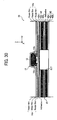
- the IC chip is covered by the resin film of the two terminal members 14a, 14b (see FIG. 30 ).
- the position of the RFID tag 11 is shifted from the center of the slit SLT.
- a sheet displaying a bar code, a product name, or a serial number may be attached on the surface of the RFID tag 11.
- the metal film 42a of the packaging bag 40 and the metal film of the RFID tag 11 are tightly fixed through the resin film by an adhesive, a capacitor is formed between the packaging bag 40 and the RFID tag 11. Therefore, a high-frequency alternating current in the UHF band that occurred in the metal film 42a of the packaging bag 40 flows to the metal film of the RFID tag 11 (called “capacitive short").
- the electromagnetic waves are radiated on both sides of each sheet 42 (in the +Z and -Z directions). That is, a portion of the packaging bag 40 acts as a large antenna.
- the RFID tag 11 is applied to the radio communication system using radio waves of a high frequency band (UHF band or microwave band). Therefore, it is possible to supply power to the IC chip 12 of the RFID tag 11 via radio waves and to secure a communication distance of 1 ⁇ 10 m.
- the packaging bag 50 receives a command signal transmitted from the RW device 20, and the tag information stored in the memory of the IC chip 12 is updated according to the information of the command signal. If necessary, the packaging bag 50 returns the updated tag information to the RW device 20 as a read signal.
- the RW device 20 is a reader-writer device in the RFID tag 11 as described above.
- a space area where a user can communicate between the RFID tag 11 and the RW device 20 is referred to as an "effective communication area."
- the RW device 20 shown in the FIG. 28 is applied to a handy type. It is also possible to use a stationary type or a fixed gate type.
- the RW device 20 reads the unique ID number from the RFID tag 11, the RW device 20 informs the management device 30 of a "detection information" via a data transmission line.
- the detection information is a number identified by the RW device 20 and a reading date/time.
- the RW device 20 sends the detection information to the RFID tag 11 to be recorded on the RFID tag 11.
- the management device 30 includes a CPU, a memory ROM in which various data used in executing a program by the CPU is stored, a hard disk device, an input device, and a display device, etc.
- the hard disk device includes a hard disk unit on which information is recorded and a drive unit for reading and writing for the hard disk in response to an instruction from the CPU.
- the input device is appropriately applied to a keyboard, a mouse, a tablet terminal, a touch panel or a light pen, and informs the CPU of information that a user input.
- the input device may communicate with the CPU by wireless manner.
- the display device includes a display unit using a liquid crystal display (LCD) or plasma display panel (PDP), and displays various information specified by the CPU. A user can utilize a touch panel LCD so that the input device and the display device are combined.
- the management device 30 is configured to generate an interrupting signal in response to contact from the RW device 20.
- a user enters the effective communication area with the RW device 20, and sends a command signal to the RFID tag packaging bag 50 the by controlling the RW device 20.
- the RFID tag 11 transmits some signal including the ID number to the RW device 20 in response to the command signal.
- the RW device 20 After receiving the signal from the RFID tag 11, the RW device 20 extracts the ID number, and sends the detection information to both the RFID tag 11 and the management device 30.
- the management device 30 shows the user the detection information on the display unit of the display device at the same time as the detection information is recorded on the hard disk. Thus, the user can ascertain that the storage of information about the RFID tag 11 corresponding to the ID number (the detection information, etc.) is completed.
- the action of shear force is generated by a user hand in this case.
- a user may use a cutting tool such as scissors.
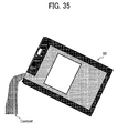
- the user can open the RFID tag packaging bag 50 in the manner described above, and take the content (a packaged item) out (see FIG. 35 ).
- the RFID tag packaging bag 50 is cut along the imaginary line and opened, the slit is broken and the slit antenna does not work.
- the RW device 20 recognizes a "communication failure" that the RW device 20 cannot communicate with the RFID tag 11.
- the "communication failure" includes both non-communication and poor communication.
- the poor communication for example, means a state with a communication distance being significantly shorter than usual.
- the RW device 20 sends an opening information to the management device 30 and the opening information is stored on the hard disk in the management device 30.
- the user can manage opening of the packaging bag 40 and reusing. For example, when medical goods such as syringes and/or medicines, etc. in the package are used in a medical operating room, the user can check a number of the medical goods rapidly and replenish soon for the next operation effectively.
- the IC chip 12 is located away enough from the imaginary line, the IC chip 12 is not likely to fall off when opening the packaging bag 40.
- the IC chip 12 and the terminal member 14b may be separated from each other when opening, if the terminal member 14b is composed of a harder material against shear force. Therefore, the perforations in the terminal member 14b have the terminal member 14b cut on the imaginary line easily as described above.
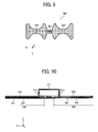
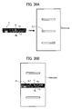
- a scrap part 51 of the RFID tag packaging bag 50 is attached to a metal plate having a slit (see FIG. 36A )
- the user can read the information including the ID number stored in the IC chip 12 out (see FIG. 36B ).
- a remaining part of the terminal member 14b and the terminal member 14a in the scrap part 51 are attached across the slit formed in the metal plate.
- the user may take a remaining part of the RFID tag 11 out from the scrap part attached to the metal plate (see FIG. 37 ). Further, if the size in the Y-axis direction of the terminal member 14b is designed to be longer in advance, the RFID tag 11 can be reused multiple times.
- steps (A-1) and (A-2) may be in a reverse order.
- a packaging bag has a cutting line on the +Y side of the packaging bag and a slit and an RFID tag on -Y side of the packaging bag. After cutting the packaging bag, the attached RFID tag can communicate with a RW device and not generate a "communication failure", since the remaining metal film is large enough.
- a packaging bag has a cutting line on the +Y side of the packaging bag and a slit and an RFID tag at a position far from the cutting line. After cutting the packaging bag, the attached RFID tag can communicate with a RW device and not generate a "communication failure", since the remaining metal film is large enough.
- the metal film 42a is made to function as an antenna part of the packaging bag 40. Therefore, the RFID tag packaging bag 50 is designed so that the size (area) of the metal film of the scrap part after cutting is too small to communicate.
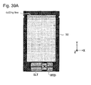
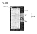
- a cutting line is located above a slit. Also in this case, the packaging bag with the attached RFID tag cannot communicate with the RW device after cutting and generates a "communication failure", since the scrap part of the packaging bag attached to the RFID tag does not have the slit and is not working as a slot antenna (see FIG. 40B ). Therefore, a user can ascertain opening information.
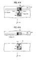
- a slit is located above a cutting line. Also in this case, a packaging bag with the attached RFID tag cannot communicate with the RW device after cutting and generates a "communication failure", since the scrap part of the packaging bag has the slit only (not an IC chip), and a main part of packaging bag attached to the RFID tag does not have the slit (see FIG. 41 B) . Therefore, a user can ascertain opening information.
Landscapes
- Engineering & Computer Science (AREA)
- Microelectronics & Electronic Packaging (AREA)
- Physics & Mathematics (AREA)
- Computer Hardware Design (AREA)
- General Physics & Mathematics (AREA)
- Theoretical Computer Science (AREA)
- Health & Medical Sciences (AREA)
- Toxicology (AREA)
- General Engineering & Computer Science (AREA)
- Computer Security & Cryptography (AREA)
- Electromagnetism (AREA)
- General Health & Medical Sciences (AREA)
- Artificial Intelligence (AREA)
- Computer Vision & Pattern Recognition (AREA)
- Packages (AREA)
- Details Of Rigid Or Semi-Rigid Containers (AREA)
Applications Claiming Priority (1)
| Application Number | Priority Date | Filing Date | Title |
|---|---|---|---|
| JP2013101801A JP2014222423A (ja) | 2013-05-14 | 2013-05-14 | Rfidタグ付き包装体、rfidシステム、及びrfidタグ付き包装体の使用方法 |
Publications (1)
| Publication Number | Publication Date |
|---|---|
| EP2804133A1 true EP2804133A1 (de) | 2014-11-19 |
Family
ID=50897349
Family Applications (1)
| Application Number | Title | Priority Date | Filing Date |
|---|---|---|---|
| EP14168172.6A Withdrawn EP2804133A1 (de) | 2013-05-14 | 2014-05-13 | Packung mit RFID-Etikett und RFID-System |
Country Status (3)
| Country | Link |
|---|---|
| US (1) | US20140340198A1 (de) |
| EP (1) | EP2804133A1 (de) |
| JP (1) | JP2014222423A (de) |
Cited By (3)
| Publication number | Priority date | Publication date | Assignee | Title |
|---|---|---|---|---|
| CN106295773A (zh) * | 2016-08-08 | 2017-01-04 | 深圳劲嘉集团股份有限公司 | 带有射频识别天线的卡纸及生产工艺 |
| CN106273669A (zh) * | 2016-08-08 | 2017-01-04 | 深圳劲嘉集团股份有限公司 | 射频识别标签的生产装置及工艺 |
| ITUB20159744A1 (it) * | 2015-12-23 | 2017-06-23 | Luxottica Srl | Occhiale con dispositivo di identificazione. |
Families Citing this family (9)
| Publication number | Priority date | Publication date | Assignee | Title |
|---|---|---|---|---|
| WO2013085076A1 (en) * | 2011-12-09 | 2013-06-13 | Ricoh Company, Ltd. | Rfid tag, rfid system, and package including rfid tag |
| US10678382B2 (en) | 2014-04-22 | 2020-06-09 | Avery Dennison Retail Information Services, Llc | Methods and systems for monitoring medication compliance |
| US10762753B2 (en) | 2014-12-12 | 2020-09-01 | Avery Dennison Retail Information Services, Llc | Methods and systems for determining the time at which a seal was broken |
| US10913594B2 (en) | 2015-07-07 | 2021-02-09 | Avery Dennison Retail Information Services, Llc | Smart ejection trays for use with medication containers |
| US10896301B2 (en) | 2015-07-07 | 2021-01-19 | Avery Dennison Retail Information Services, Llc | RFID-based methods and systems for monitoring medication compliance |
| US20180012117A1 (en) * | 2016-07-07 | 2018-01-11 | Avery Dennison Retail Information Services, Llc | Medication containers incorporating wireless communication devices and methods for manufacturing such containers |
| JP7742725B2 (ja) * | 2021-06-08 | 2025-09-22 | 株式会社Uacj | 開封検知シート、包装材 |
| CN114863655A (zh) * | 2022-05-06 | 2022-08-05 | 独角兽网络科技(苏州)有限公司 | 一种用于监测提醒的智能装置及方法 |
| JP7718458B2 (ja) * | 2023-09-27 | 2025-08-05 | いすゞ自動車株式会社 | 検知システム |
Citations (3)
| Publication number | Priority date | Publication date | Assignee | Title |
|---|---|---|---|---|
| US20020126057A1 (en) * | 2000-07-18 | 2002-09-12 | King Patrick F. | Wireless communication device and method |
| US20060017545A1 (en) * | 2004-03-26 | 2006-01-26 | Volpi John P | Radio frequency identification interrogation systems and methods of operating the same |
| US20090027206A1 (en) * | 2007-07-27 | 2009-01-29 | Yuen Foong Yu Paper Mfg. Co. Ltd. | Radio frequency identification tag, method of fabricating the same, and method of using the same |
Family Cites Families (19)
| Publication number | Priority date | Publication date | Assignee | Title |
|---|---|---|---|---|
| US5093206A (en) * | 1990-03-09 | 1992-03-03 | E. I. Du Pont De Nemours And Company | Curable laminated article of epdm elastomer and ethylene-containing polymer |
| JPH06282229A (ja) * | 1993-01-27 | 1994-10-07 | Unitika Ltd | 盗難防止ラベル |
| CA2402674A1 (en) * | 2000-03-15 | 2001-09-20 | International Paper | Tamper evident radio frequency identification system and package |
| US6794000B2 (en) * | 2001-07-17 | 2004-09-21 | Intermec Ip Corp. | Tamper evident label with transponder employing multiple propagation points |
| CN1898686A (zh) * | 2003-12-24 | 2007-01-17 | 新加坡科技物资管理私人有限公司 | Rfid密封标签 |
| US7842156B2 (en) * | 2005-04-27 | 2010-11-30 | Avery Dennison Corporation | Webs and methods of making same |
| JP4787572B2 (ja) * | 2005-08-25 | 2011-10-05 | 株式会社日立製作所 | 無線icタグ、及び無線icタグの製造方法 |
| WO2007119304A1 (ja) * | 2006-04-14 | 2007-10-25 | Murata Manufacturing Co., Ltd. | 無線icデバイス |
| JP2008143589A (ja) * | 2006-12-13 | 2008-06-26 | Dainippon Printing Co Ltd | Icタグ付き包装パッケージ |
| US20080180217A1 (en) * | 2007-01-25 | 2008-07-31 | Avery Dennison Corporation | RFID tag |
| JP5028176B2 (ja) * | 2007-07-25 | 2012-09-19 | 株式会社日立製作所 | Rfidタグ実装パッケージおよびその製造方法 |
| JP5169109B2 (ja) * | 2007-09-27 | 2013-03-27 | 凸版印刷株式会社 | 非接触icラベル |
| US8042739B2 (en) * | 2007-09-28 | 2011-10-25 | The United States Of America As Represented By The Administrator Of The National Aeronautics And Space Administration | Wireless tamper detection sensor and sensing system |
| JP5136022B2 (ja) * | 2007-11-27 | 2013-02-06 | 大日本印刷株式会社 | 開梱確認用の非接触icタグ及び非接触icタグを用いた開梱確認方法 |
| JP5384027B2 (ja) * | 2008-05-01 | 2014-01-08 | 押尾産業株式会社 | 包装体及びその製造方法 |
| JP5113727B2 (ja) * | 2008-11-20 | 2013-01-09 | 株式会社日立製作所 | 無線icタグ |
| US20110285507A1 (en) * | 2010-05-21 | 2011-11-24 | Nelson Erik T | Tamper Detection RFID Tape |
| US20110313894A1 (en) * | 2010-06-18 | 2011-12-22 | Dye Alan W | System and Method for Surgical Pack Manufacture, Monitoring, and Tracking |
| US8884764B2 (en) * | 2011-02-25 | 2014-11-11 | Avery Dennison Corporation | Method, system, and apparatus for RFID removal detection |
-
2013
- 2013-05-14 JP JP2013101801A patent/JP2014222423A/ja active Pending
-
2014
- 2014-05-13 EP EP14168172.6A patent/EP2804133A1/de not_active Withdrawn
- 2014-05-14 US US14/277,534 patent/US20140340198A1/en not_active Abandoned
Patent Citations (3)
| Publication number | Priority date | Publication date | Assignee | Title |
|---|---|---|---|---|
| US20020126057A1 (en) * | 2000-07-18 | 2002-09-12 | King Patrick F. | Wireless communication device and method |
| US20060017545A1 (en) * | 2004-03-26 | 2006-01-26 | Volpi John P | Radio frequency identification interrogation systems and methods of operating the same |
| US20090027206A1 (en) * | 2007-07-27 | 2009-01-29 | Yuen Foong Yu Paper Mfg. Co. Ltd. | Radio frequency identification tag, method of fabricating the same, and method of using the same |
Cited By (5)
| Publication number | Priority date | Publication date | Assignee | Title |
|---|---|---|---|---|
| ITUB20159744A1 (it) * | 2015-12-23 | 2017-06-23 | Luxottica Srl | Occhiale con dispositivo di identificazione. |
| WO2017108981A1 (en) * | 2015-12-23 | 2017-06-29 | Luxottica S.R.L. | Eyeglasses with identification device |
| US10877299B2 (en) | 2015-12-23 | 2020-12-29 | Luxottica S.R.L. | Eyeglasses with identification device |
| CN106295773A (zh) * | 2016-08-08 | 2017-01-04 | 深圳劲嘉集团股份有限公司 | 带有射频识别天线的卡纸及生产工艺 |
| CN106273669A (zh) * | 2016-08-08 | 2017-01-04 | 深圳劲嘉集团股份有限公司 | 射频识别标签的生产装置及工艺 |
Also Published As
| Publication number | Publication date |
|---|---|
| US20140340198A1 (en) | 2014-11-20 |
| JP2014222423A (ja) | 2014-11-27 |
Similar Documents
| Publication | Publication Date | Title |
|---|---|---|
| EP2804133A1 (de) | Packung mit RFID-Etikett und RFID-System | |
| EP3503289B1 (de) | Rfid-inlay mit einer massefläche | |
| US9871294B2 (en) | Dual band RFID device and method of formation | |
| EP1758050B1 (de) | RFID-Etikett und Herstellungsverfahren dafür | |
| CN102298722B (zh) | 无线标签及制造方法 | |
| EP3032649A1 (de) | Verpackung mit daran befestigtem ic-drahtlosetikett und herstellungsverfahren für verpackung mit daran befestigtem ic-drahtlosetikett | |
| CN101208827A (zh) | 射频识别标签 | |
| US9691016B2 (en) | RFID tag for a package of tablets | |
| JP5687154B2 (ja) | Rfidタグ及びrfidシステム | |
| JP2015060260A (ja) | 通信装置、通信システム、及び通信装置の使用方法 | |
| JP2008092198A (ja) | Rfidラベルタグおよびその製造方法 | |
| JP2015162187A (ja) | Rfidタグ、通信システム、及びrfidタグの使用方法 | |
| JP6025046B2 (ja) | Rfidタグ及びrfidシステム | |
| JP6065464B2 (ja) | Rfidタグ付きタブレットパッケージ | |
| JP2014041444A (ja) | Rfidタグ及びrfidシステム | |
| JP5715663B2 (ja) | ハンディアンテナ、棚卸装置、棚卸システム及び棚卸方法 | |
| JP2015170246A (ja) | Rfidタグ付きパッケージの製造方法、及びrfidタグ付きパッケージ | |
| KR20150122040A (ko) | Nfc 기능이 내장된 전자 가격 표시기 | |
| JP2015170247A (ja) | Rfidタグ付きパッケージ、及びrfidタグ付きパッケージの製造方法 | |
| JP2014041443A (ja) | Rfidタグ及びrfidシステム | |
| TWM512173U (zh) | 具雷射直接成型天線之無線射頻辨識標籤裝置 | |
| JP2014042127A (ja) | Rfidタグ及びrfidシステム |
Legal Events
| Date | Code | Title | Description |
|---|---|---|---|
| PUAI | Public reference made under article 153(3) epc to a published international application that has entered the european phase |
Free format text: ORIGINAL CODE: 0009012 |
|
| 17P | Request for examination filed |
Effective date: 20140513 |
|
| AK | Designated contracting states |
Kind code of ref document: A1 Designated state(s): AL AT BE BG CH CY CZ DE DK EE ES FI FR GB GR HR HU IE IS IT LI LT LU LV MC MK MT NL NO PL PT RO RS SE SI SK SM TR |
|
| AX | Request for extension of the european patent |
Extension state: BA ME |
|
| 17Q | First examination report despatched |
Effective date: 20160602 |
|
| STAA | Information on the status of an ep patent application or granted ep patent |
Free format text: STATUS: THE APPLICATION IS DEEMED TO BE WITHDRAWN |
|
| 18D | Application deemed to be withdrawn |
Effective date: 20161013 |